EP4564216A1 - Detection and mitigation of volt boot attacks - Google Patents
Detection and mitigation of volt boot attacks Download PDFInfo
- Publication number
- EP4564216A1 EP4564216A1 EP24215551.3A EP24215551A EP4564216A1 EP 4564216 A1 EP4564216 A1 EP 4564216A1 EP 24215551 A EP24215551 A EP 24215551A EP 4564216 A1 EP4564216 A1 EP 4564216A1
- Authority
- EP
- European Patent Office
- Prior art keywords
- power domain
- volt
- power
- flag
- voltage
- Prior art date
- Legal status (The legal status is an assumption and is not a legal conclusion. Google has not performed a legal analysis and makes no representation as to the accuracy of the status listed.)
- Granted
Links
Images





Classifications
-
- G—PHYSICS
- G06—COMPUTING OR CALCULATING; COUNTING
- G06F—ELECTRIC DIGITAL DATA PROCESSING
- G06F21/00—Security arrangements for protecting computers, components thereof, programs or data against unauthorised activity
- G06F21/70—Protecting specific internal or peripheral components, in which the protection of a component leads to protection of the entire computer
- G06F21/71—Protecting specific internal or peripheral components, in which the protection of a component leads to protection of the entire computer to assure secure computing or processing of information
- G06F21/75—Protecting specific internal or peripheral components, in which the protection of a component leads to protection of the entire computer to assure secure computing or processing of information by inhibiting the analysis of circuitry or operation
- G06F21/755—Protecting specific internal or peripheral components, in which the protection of a component leads to protection of the entire computer to assure secure computing or processing of information by inhibiting the analysis of circuitry or operation with measures against power attack
-
- G—PHYSICS
- G06—COMPUTING OR CALCULATING; COUNTING
- G06F—ELECTRIC DIGITAL DATA PROCESSING
- G06F21/00—Security arrangements for protecting computers, components thereof, programs or data against unauthorised activity
- G06F21/50—Monitoring users, programs or devices to maintain the integrity of platforms, e.g. of processors, firmware or operating systems
- G06F21/55—Detecting local intrusion or implementing counter-measures
- G06F21/554—Detecting local intrusion or implementing counter-measures involving event detection and direct action
-
- G—PHYSICS
- G06—COMPUTING OR CALCULATING; COUNTING
- G06F—ELECTRIC DIGITAL DATA PROCESSING
- G06F21/00—Security arrangements for protecting computers, components thereof, programs or data against unauthorised activity
- G06F21/70—Protecting specific internal or peripheral components, in which the protection of a component leads to protection of the entire computer
- G06F21/81—Protecting specific internal or peripheral components, in which the protection of a component leads to protection of the entire computer by operating on the power supply, e.g. enabling or disabling power-on, sleep or resume operations
-
- G—PHYSICS
- G06—COMPUTING OR CALCULATING; COUNTING
- G06F—ELECTRIC DIGITAL DATA PROCESSING
- G06F2221/00—Indexing scheme relating to security arrangements for protecting computers, components thereof, programs or data against unauthorised activity
- G06F2221/03—Indexing scheme relating to G06F21/50, monitoring users, programs or devices to maintain the integrity of platforms
- G06F2221/034—Test or assess a computer or a system
Definitions
- This disclosure relates generally to the power management of electronic circuits, and more specifically to the detection and mitigation of a volt boot attack on a power supply pin used to retain volatile contents of the electronic circuit.
- a volt boot attack is an attack of an electronic circuit which seeks to retain, and thereby gain access to, the contents of an embedded volatile storage during power down or during a transition to a low power operating mode.
- the volatile storage will store sensitive data (e.g., secret keys), resulting from a secure computation by the electronic circuit.
- the attacker Prior to a power down or entering a low power mode, the attacker will drive a power supply pin with sufficient voltage to keep the data in the volatile storage from decaying and thus becoming corrupted. When the circuit is subsequently powered up again and rebooted, the attacker may then have access to the sensitive data stored in the volatile storage.
- Detection of a volt boot attack is difficult because the attack sequence must be distinguished from a normal transition to a low power operation mode and a subsequent recovery when the circuit is to be used for computation.
- the system relies upon voltage decay to erase stored data when power is removed, rather than directly performing erase operations in the memory.
- modern systems often have multiple power domains to optimize various system level use cases, hence transitions between normal operating voltages and low power modes may be frequent and involve numerous combinations of power domains.
- Embodiments described herein provide for the detection and mitigation of volt boot attacks of an electronic circuit (e.g., an SoC).
- An SoC may store a variety of sensitive data such as passwords, secret encryption keys or security codes. This sensitive data may be stored in volatile storage elements including, but not limited to, a Static Random Access Memory (SRAM), a Dynamic Random Access Memory (DRAM), a Central Processing Unit (CPU), registers or a Cache.
- Volt boot attacks involve an attacker driving a voltage on a power supply pin to drive at least a minimum retention voltage to retain the sensitive data in the volatile storage during power cycles. Thus, the attacker may gain access to the sensitive data.
- the embodiments described herein monitor voltage supply lines during power cycling or low power mode transitions and compare previous and requested supply line states to detect an attempt to override the supply line values otherwise controlled by the SoC. Additionally, after detecting a volt boot attack, a repower cycle may be applied to all power domains of the SoC to force erasure of the sensitive data and thus mitigate the attack.
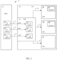
- FIG. 1 shows an embodiment 10 of an electronic system under attack by a volt boot attack.
- the embodiment 10 includes a PMIC 12 to provide supply voltages on pin0 14, pin 1 16 and pin2 18.
- the PMIC 12 supplies power to an SoC 20, (or similar electronic circuit). Specifically, the SoC 20 receives power from the pins 14, 16 and 18 with a PMC 22.
- the PMC 22 includes Low Voltage Detectors (LVD) (not shown) and power switches, which then provide controlling voltages to power domains 24a, 24b and 24c (generally 24), over respective nets 26a, 26b and 26c (generally 26).
- power domains 24a and 24b include respective volatile storage elements (e.g., SRAMs), and where the supply voltage to pin1 16 is maintained above a retention voltage by an attackers probe point 28 regardless of whether the supply voltages from the PMIC 12 are power cycled or transitioned to a lower voltage.
- FIG. 2 shows further detail of the embodiment 10 of FIG. 1 .
- the PMIC 12 shows the PMIC 12 having voltage regulators 30a, 30b and 30c, (generally 30) to regulate and supply the supply voltages on respective pins 14, 16 and 18.
- the supply voltages supply respective Low Dropout Oscillators (LDO) 32a, 32b and 32c, (generally 32).
- LDO Low Dropout Oscillators
- the SoC 20 subsequently compares each supply voltage with a respective LVD (not shown) in the SPSD.
- the LVDs are located in the SPSD in one non-limiting embodiment, however may be co-located with other functional blocks in other embodiments.
- volatile storage elements 34a and 34b (generally 34) powered by and included within respective power domains 24a and 24b.
- the methods for detecting and mitigating a volt boot attack on pin2 18 are applicable to other structures within the power domain 24c that are intentionally altered by a reduction of supply voltage below a predetermined threshold.
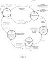
- FIG. 3 shows a method 40 of operation of the system of FIG. 2 .
- an attacker is physically in possession of the SoC 20. Prior to the attack, at 42, a first power cycle of the SoC 20 is performed. At 44, the SoC 20 then completes a boot sequence. At 46, a secure computation may be executed with secret keys (or other sensitive data) stored in a volatile memory. In the absence of an attack, the secret keys may be quickly erased by power cycling the SoC, rather than incurring a penalty (e.g., 10s of seconds) during a boot operation. However, at 48, the attacker performs an adversarial action by driving the supply pin (e.g., pin 16), powering the volatile memory, with a probe to retain the memory contents.
- the supply pin e.g., pin 16
- the SoC 20 is transitioned to a low power mode, initiated either by the SoC 20 or the attacker.
- a second power cycle of the SoC 20, (or a return from a low power mode to a normal operating mode) is performed.
- the SoC 20 may reboot with the secret keys still retained in memory. Thus, the attacker may now access the secret keys from the volatile memory.
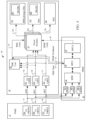
- FIG. 4 shows an embodiment 60 of the system of FIG. 2 with an SPMC 62 added for the detection and mitigation of volt boot attacks.
- the boundaries of the SoC 20 are drawn to be consistent with FIG. 1 and FIG. 2 .
- the various functions PMIC 12, LDO 32, PMC core 80, power switches 74, power domains 24 and the SPMC 62 may be partitioned into separate modules or combined in any combination on one or more monolithic substrates.
- the SPMC 62 includes an SPSD 64a, 64b and 64c (generally 64) for reach respective pin 14, 16 and 18 and electrically coupled to each respective power domain 24a, 24b and 24c.
- Each SPSD 64 is configured to generate a flag for each respective power domain 24 to provide an indication of supply voltage status and changes on the pins 14, 16 and 18.
- Each of the SPSD 64 are connected to an SPSF 66.
- the SPSF 66 configures an inactive flag from each respective power domain 24 that is not required for the normal mode of operation of the SoC 20.
- the SPSF 66 further aggregates each flag received from the SPSD 64 that does not have an inactive flag set, to define a previous state for each flag, and sends the flag information to the SPCC 68.
- the SPCC 68 receives requested power domain settings from the PMC core 80 over a PMC state bus 76 and provides feedback to the PMC core 80 over an SPMC feedback bus 78.
- the PMC core 80 requests over a PMC control bus 82, at least one power domain 24 to transition to a lower voltage level, (below the LVD level of the respective LVD).
- a voltage on pins 14, 16 and 18 that is determined to be below the respective LVD level by the LVD detectors controls a respective LDO 32, the status of which is communicated to the PMC core 80 over respective nets 72a, 72b and 72c (generally 72).
- the SPCC 68 compares the flag for each power domain 24 transitioned to the lower voltage level to the previous state set by the SPSF 66.
- a volt boot attack is presumed to have occurred on the pin (e.g., 14, 16 or 18) associated with the respective power domain 24.
- the RPCA 70 will perform a power cycle with all of the power domains 24 in response to a volt boot attack, by controlling a plurality of switches 74 over a SPMC control bus 84. By power cycling all of the power domains 24, including ones not directly attacked, this ensures that sensitive data is not leaked across domains and thus becoming obtained indirectly by the attacker.
- power cycling includes reducing the operating voltages of all domains below their respective LVD levels for a predetermined period of time, then restoring the operating voltages to their previous values.
- the predetermined period of time may be equal to at least the time necessary for a volatile storage to decay to a level where data is unreadable.
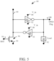
- FIG. 5 shows implementation details of one embodiment of the SPSD 64.
- the SPSD 64 may include a monitored supply 90, which is the positive supply of the inverters 102 and 104 that form a latch.
- the SPSD 64 may be connected to a ground terminal 92, which is the negative supply of the inverters 102 and 104.
- a reset (RST) signal 94 controls a transistor 96 configured to discharge the node 99 towards the ground terminal 92 when the RST signal 94 is a logical "1".
- a circuit load 98 is between an SPSD flag 100 output and the ground terminal 92.
- the monitored supply 90 is initially below a brown-out level (Vbrown), defined as a voltage below the low voltage detection level of the LVDs. Accordingly, the SPSD flag 100 initially discharges to a logical "0". After the power supplies are ramped to an operating voltage above Vbrown and RST is asserted to a logical "1", the transistor 96 will discharge node 99 and cause the latch formed by inverters 102 and 104 to drive the SPSD flag 100 to a logical "1". This may be considered to "arm" the SPSD for the next power cycle. After a subsequent power cycle, the SPCC 68 will read the state of the SPSD flag 100.
- Vbrown brown-out level
- V_in Vbrown 0 1
- SPCC reads SPSD flags. If flags are not 0, then supply never went below Vbrown-out, thus inferring a volt boot attack.
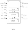
- FIG. 6 shows implementation details of one embodiment of the SPCC 68.
- the SPCC 68 may include a Finite State Machine (FSM), SPCC_FSM 110 to sequence the actions of the SPCC 68.
- the SPCC_FSM 110 may communicate with a Power Recycling Interaction Unit 112 to communicate with the RPCA 70 during power recycling.
- the Power Recycling Interaction Unit 112 may communicate with a Control and Status Register 114 configured to assist with control the SPCC 68 and store various status of the SoC 20.
- FSM Finite State Machine
- the SPCC 68 receives a plurality of signals, specifically an SPSF_flag_i 120 from a respective SPSD 64, a PD_req_i 122 from a respective power domain, a POR 124 (power on reset), a PS_i 126 from a respective power switch 74, an LVD_i 130 from a respective LVD, an HVD i (high voltage detector, not shown) 132 and a Reset Req 134 (reset request) from a PMC core 80.
- the SPCC 68 receives a PMC _Requested_State 136 and a PMC_Previous_State 138 from the PC core 80.
- the SPCC 68 transmits an Instruct_RPCA 140, to instruct the RPCA 70, and receives a Power Cycle _Comp 142 from the RPCA 70 to inform the SPCC 68 when the power cycle has completed so that the PMC core 80 may resume operation depending upon the SPCC severity flag settings.
- FIG. 7 shows implementation details of one embodiment of the RPCA 70.
- the RPCA 70 may include an FSM, RPCA_FSM 150 to sequence the actions of the RPCA 70.
- the RPCA_FSM 150 may communicate with a Control and Status Register 152 configured to assist with control the RPCA 70 and store various status of the SoC 20.
- the RPCA 70 receives a plurality of signals, namely a PD_req_i 122, a POR 124 and a Reset Req 134 as previously described for FIG. 6 .
- the RPCA 70 transmits a "To_Power_Off_Modules_i" 154 signal to a respective power switch 74 for power cycling.
- the RPCA 70 receives the "Instruct_RPCA” 140 from the SPCC 68 and transmits the "Power_Cycle_Comp" 142 to the SPCC 68.
- FIG. 8 shows an embodiment 160 of the operation of the SPCC 68 of FIG. 6 .
- the SPCC 68 begins in an Idle State 162. If no power cycle is requested at 164, the SPCC 68 remains in the Idle State 162. If a power cycle is requested at 166, the SPCC 68 transitions to a Detection State 168. At 168, the SPCC 68 compares a requested state of the PMC to a previous state (as set by the flags from the SPSD 64, which do not include inactive power domains 24). If no volt boot attack is detected the SPCC 68 transitions at 170 back to the Idle State 162. Otherwise, the SPCC 68 transitions at 172 to the Attack Mitigation State 174.
- the SPCC68 instructs the RPCA 70 to perform a power cycle on all power domains 24, then at 176 transitions to the Forced Power Cycling State 178.
- the power cycling is performed for a predetermined period of time, during which the SPCC 68 remains in the Forced Power Cycling State 178 as checked at 180.
- the SPCC 68 transitions at 182 to a Check Severity Configuration 184 state, where the system RST 94 is generated and applied. After checking the severity flag settings, the SoC 20 will transition at 186 to the intended operating mode and then return to the Idle State 162.
- a severity flag setting of " 11" means that the SoC 20 can return to a normal mode of operation after mitigating the volt boot attack.
- a severity flag setting of "10” means the SoC 20 can return to a non-secure mode after mitigating the volt boot attack.
- a severity flag setting of "01” or "00” means that the SoC 20 cannot exit the reset state after detecting the volt boot attack.
- the severity flag definitions may be hardwired (e.g., with an electronic e-fuse) during production of the SoC 20.
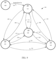
- FIG. 9 shows an embodiment 190 of the operation of the PMC Core 80, illustrating the scope (e.g., a possibility of occurrence) of volt boot attacks.
- State transitions of the PMC core 80 are shown for three power domains 24 (see FIG. 1 , 2 and 4 ) with a voltage scalar [V0, V1, V2] shown in each state to represent whether the operating voltage is above the lower voltage detection level (shown as " 1"), or below the lower voltage detection level (shown as "0").
- V0 voltage supply is assumed to always be on or in the " 1" state, which corresponds to the power domain PD0 24a of FIG. 4 .
- each double wide arc shows a transition path where a volt boot attack is possible.
- Each single wide arc shows a transition path where a volt boot attack is not possible, nor detectable because a supply voltage is only powering up, not down.
- the SoC 20 executes a boot sequence at 194 to reach a "111 state” 196 (e.g. voltage scalar is "111").
- a "111 state” 196 e.g. voltage scalar is "111"
- V1 and V2 of the voltage scalar [V0, V1, V2] the subsequently described voltage transitions will only occur with V1 and V2 of the voltage scalar [V0, V1, V2].
- a transition from the 111 state 196 to the 110 state 198 by the transition 200 occurs if the power domain 24c is requested to be put in a lower voltage state. Specifically, the previous PMC state is 1,1,1 and the requested PMC state is 110. If an attacker holds the V2 voltage above the lower voltage detection threshold, then a volt boot attack may occur.
- the transition 202 from the 110 state 198 back to the 111 state 196 will not result in a volt boot attack because V2 is requested to be powered up, but there is no request for powering down
- the transition 206 from the 111 state 196 to a 101 state 204 may result in a volt boot attack on V1.
- the transition 208 from the 101 state 204 to the 111 state 196 will not expose the SoC 20 to a volt boot attack because no voltage is being requested to decrease, in which case the SPSD flag need not be checked.
- the transition 212 from the 111 state 196 to a 100 state 210 may result in a volt boot attack on V1 or V2.
- the transition 214 from the 100 state 210 to the 111 state 196 will not expose the SoC 20 to a volt boot attack.
- the transition 216 from the 110 state 198 to the 100 state 210 may result in a volt boot attack on V1.
- transition 218 from the 100 state 210 to the 110 state 198 will not expose the SoC 20 to a volt boot attack.
- the transition 220 from the 101 state 204 to the 100 state 210 may result in a volt boot attack on V2.
- the transition 222 from the 100 state 210 to the 101 state 204 will not expose the SoC 20 to a volt boot attack.
- the transition 224 from the 110 state 198 to the 101 state 204 may result in a volt boot attack on V1.
- the transition 226 from the 101 state 204 to the 110 state 198 may also expose the SoC 20 to a volt boot attack on V2.
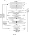
- FIG. 10 shows an embodiment 230 of a method for detection and mitigation of a volt boot attack, in accordance with an embodiment of the present disclosure.
- the method starts.
- a power up sequence is requested.
- the PORs are asserted and all supplies ramp above the LVD level (or RAM retention level).
- the SPSD flags are reset by the SPCC 68.
- the SoC 20 performs an operation to generate secure data, which the user of the SoC 20 may wish to protect.
- at least one power domain 24 mode transition is request by the PMC, and accordingly a voltage supply level is changed.
- a verification is made to determine if a device (SoC 20) power off request has been made to the PMC core 80. If a power request was made, then the system shuts down at 246, and then the method stops at 266.. Otherwise, at 248, the SPCC 68 compares the previous and requested PMC states for each power domain 24. At 250, a verification is made to determine if any power domains 24 are requested to be powered down. If no requests were made to power down a power domain 24, then the method returns to 238 to reset the SPSD flags. Otherwise, at 252 the SPCC 68 compares the SPSF 66 flag status (e.g., the requested state of each flag), with the previous state for powered down (and active) domains only.
- the SPSF 66 flag status e.g., the requested state of each flag
- a comparison is made between the requested and previous states of the flags to determine a mismatch. If there is no mismatch, then the method returns to 238 to reset the SPSD flags. Otherwise, at 256 it is determined that a volt boot attack occurred and was detected.
- the SPCC 68 instructs the RPCA 70 to initiate a power cycle for all power domains 24.
- the SPCC 68 informs the PMC core 80 of this instruction to the RPCA 70, and the PMC core 80 waits for the power cycle to complete.
- the SPCC 68 severity flag is checked to be "11". If the flag is not "11", then the severity flag is checked to be "10”.
- the SPCC 68 severity flag is set to "11” then at 268 the SoC 20 operation resumes in normal secure mode, then proceeds to 236 to reassert the PORs. If the SPCC 68 severity flag is set to "10” then at 270 the SoC 20 operation is downgraded to a non-secure mode, then proceeds to 236 to reassert the PORs.
- FIG. 11 shows an embodiment 280 of a method for detection and mitigation of a volt boot attack, in accordance with an embodiment of the present disclosure.
- a respective operating voltage is applied to at least one power domain 24.
- the operating voltage exceeds a low voltage detection level of a respective LVD.
- a flag is set for each power domain to define a previous state of the corresponding supply pin.
- at least one power domain 24 is requested to transition to a respective lower voltage (less than the respective LVD level).
- the respective flag of the previous state is compared with the requested state to determine a mismatch.
- an occurrence of a volt boot attack is determined from the mismatch.
- FIG. 12 shows an embodiment 300 of a method for detection and mitigation of a volt boot attack, in accordance with an embodiment of the present disclosure.
- an operating voltage is applied to a power domain 24.
- the operating voltage exceeds a retention voltage level of a volatile storage element.
- a flag is set for the power domain to define a previous state of corresponding supply pin.
- the power domain 24 is requested to transition to a lower voltage, less than the retention level.
- the respective flag of the previous state is compared with the requested state to determine a volt boot attack.
- the volt boot attack is mitigated by power cycling the power domain 24.
- a method for detection and mitigation of volt boot attacks comprises applying a respective operating voltage to at least one power domain, wherein each respective operating voltage exceeds a low voltage detection level of the respective power domain.
- a flag is set for each of the at least one power domain, having the respective operating voltage applied, to define a previous state for each flag.
- the at least one power domain is requested to transition to a respective lower voltage being less than the low voltage detection level for the respective power domain.
- the flag is set for each of the at least one power domain, having the respective lower voltage applied, to define a requested state for each flag.
- the previous state is compared to the requested state to determine a mismatch for each power domain. An occurrence of a volt boot attack is determined for each power domain comprising the respective mismatch.
- the volt boot attack is mitigated by power cycling each of the at least one power domain in response to an occurrence of the volt boot attack for at least one respective power domain, wherein power cycling comprises reducing each operating voltage below the respective voltage detection level followed by increasing each operating voltage above the respective voltage detection level.
- the operating voltage is reduced below the respective voltage detection level for a predefined period of time.
- An apparatus comprising the at least one power domain is returned to a normal mode of operation after mitigating the volt boot attack, in response to a severity flag setting.
- An apparatus comprising the at least one power domain is returned to a non-secure mode of operation after mitigating the volt boot attack, in response to a severity flag setting.
- An apparatus comprising the at least one power domain is returned to a reset mode of operation after mitigating the volt boot attack, in response to a severity flag setting.
- Applying the respective operating voltage to exceed the respective low voltage detection level comprises applying a voltage equal to or greater than a voltage level required to retain a data in a storage element powered by the respective power domain.
- the at least one power domain comprises multiple power domains, wherein at least one of the multiple power domain powers a volatile storage element.
- An inactive flag is set for each of the at least one power domain not required for a normal mode of operation, and wherein comparing the flag for each of the at least one power domain transitioned to the respective lower voltage excludes each power domain comprising the respective inactive flag.
- a method for detection and mitigation of volt boot attacks comprises applying an operating voltage to a power domain, wherein the operating voltage is equal to or greater than a retention voltage level required to retain a data in a storage element powered by the power domain.
- a flag is set for the power domain, having the operating voltage applied, to define a previous state for the flag.
- the power domain is requested to transition to a lower voltage being less than the retention voltage level.
- the flag for the power domain transitioned to the lower voltage is set to define a requested state.
- the previous state is compared to the requested state to determine a volt boot attack for the power domain.
- the volt boot attack is mitigated by power cycling the power domain in response to an occurrence of the volt boot attack, wherein power cycling comprises reducing the operating voltage below the retention voltage level for a predefined period of time exceeding a retention time of the storage element.
- Alternative embodiments of the method for detection and mitigation of volt boot attacks include one of the following features, or any combination thereof.
- An apparatus comprising the power domain is returned to a normal mode of operation after mitigating the volt boot attack, in response to a severity flag setting.
- An apparatus comprising the power domain is returned to a non-secure mode of operation after mitigating the volt boot attack, in response to a severity flag setting.
- An apparatus comprising the power domain is returned to a reset mode of operation after mitigating the volt boot attack, in response to a severity flag setting.
- An additional power domain of an apparatus comprising the power domain is power cycled in response to the volt boot attack.
- an apparatus comprises at least one power domain comprising a volatile storage element, wherein each power domain is connected to a respective operating voltage exceeding a low voltage detection level of the respective power domain.
- a respective Secure Probe State Detector (SPSD) is electrically coupled to each power domain, the SPSD configured to generate a flag for each respective power domain.
- a Supply Pin State Flags (SPSF) module connected to each SPSD, the SPSF module configured to set an inactive flag for each respective power domain not required for the apparatus to operate in a normal mode, and to aggregate each flag received from an SPSD not having an inactive flag that is set, to define a previous state and a requested state for each flag.
- a Secure Power Cycle Controller connected to the SPSF and a Power Management Controller (PMC), the PMC configured to request the at least one power domain to transition to a respective lower voltage being less than the low voltage detection level for the respective power domain, the SPCC configured to compare the requested state for each of the at least one power domain transitioned to the respective lower voltage to the previous state of each respective flag to determine a volt boot attack for each power domain.
- a Re-Power Cycling Actuator connected to the SPCC and at least one power switch for each power domain, the RPCA configured to power cycle each of the at least one power domain in response to a volt boot attack for any power domain.
- a Low Voltage Detection (LVD) circuit is connected to a respective power domain through a respective power switch, wherein the LVD circuit is configured to compare the respective operating voltage to the low voltage detection level.
- the low voltage detection level is a data retention level of the volatile storage element.
- the volatile storage element is a Random Access Memory.
- the volatile storage element is a Cache memory.
- the volatile storage element is a register of a processor.
Landscapes
- Engineering & Computer Science (AREA)
- Theoretical Computer Science (AREA)
- Computer Hardware Design (AREA)
- Computer Security & Cryptography (AREA)
- Software Systems (AREA)
- Physics & Mathematics (AREA)
- General Engineering & Computer Science (AREA)
- General Physics & Mathematics (AREA)
- Mathematical Physics (AREA)
- Power Sources (AREA)
Abstract
Description
- The following specification describes the invention.
- This disclosure relates generally to the power management of electronic circuits, and more specifically to the detection and mitigation of a volt boot attack on a power supply pin used to retain volatile contents of the electronic circuit.
- A volt boot attack is an attack of an electronic circuit which seeks to retain, and thereby gain access to, the contents of an embedded volatile storage during power down or during a transition to a low power operating mode. Typically, the volatile storage will store sensitive data (e.g., secret keys), resulting from a secure computation by the electronic circuit. Prior to a power down or entering a low power mode, the attacker will drive a power supply pin with sufficient voltage to keep the data in the volatile storage from decaying and thus becoming corrupted. When the circuit is subsequently powered up again and rebooted, the attacker may then have access to the sensitive data stored in the volatile storage.
- Detection of a volt boot attack is difficult because the attack sequence must be distinguished from a normal transition to a low power operation mode and a subsequent recovery when the circuit is to be used for computation. In many electronic systems, for expediency, the system relies upon voltage decay to erase stored data when power is removed, rather than directly performing erase operations in the memory. Furthermore, modern systems often have multiple power domains to optimize various system level use cases, hence transitions between normal operating voltages and low power modes may be frequent and involve numerous combinations of power domains.
- The present invention is illustrated by way of example and is not limited by the accompanying figures, in which like references indicate similar elements. Elements in the figures are illustrated for simplicity and clarity and have not necessarily been drawn to scale.
-
FIG. 1 is a schematic view of an embodiment of an electronic system under attack by a volt boot attack. -
FIG. 2 is a schematic view of the embodiment ofFIG. 1 with further detail of the Power Management Integrated Circuit (PMIC) and the System on a Chip (SoC) comprising a Power Management Controller (PMC). -
FIG. 3 is a flowchart representation of a method of operation of the system ofFIG. 2 under attack by a volt boot attack. -
FIG. 4 is a schematic view of the electronic system ofFIG. 2 further comprising a Secure Probe Management Controller (SPMC), in accordance with an embodiment of the present disclosure. -
FIG. 5 is a schematic view of a Secure Probe State Detector (SPSD), in accordance with an embodiment of the present disclosure. -
FIG. 6 is a schematic view of a Secure Power Cycle Controller (SPCC), in accordance with an embodiment of the present disclosure. -
FIG. 7 is a schematic view of a Re-Powering Cycle Actuator (RPCA), in accordance with an embodiment of the present disclosure. -
FIG. 8 is a state diagram representation of the operation of the SPCC ofFIG. 6 , in accordance with an embodiment of the present disclosure. -
FIG. 9 is a state diagram representation of the operation of the embodiment of the PMC ofFIG. 2 , illustrating the scope of volt boot attacks. -
FIG. 10 is a flowchart representation of a method for detection and mitigation of volt boot attacks, in accordance with an embodiment of the present disclosure. -
FIG. 11 is a flowchart representation of another method for detection and mitigation of volt boot attacks, in accordance with an embodiment of the present disclosure. -
FIG. 12 is a flowchart representation of another method for detection and mitigation of volt boot attacks, in accordance with an embodiment of the present disclosure. - Embodiments described herein provide for the detection and mitigation of volt boot attacks of an electronic circuit (e.g., an SoC). An SoC may store a variety of sensitive data such as passwords, secret encryption keys or security codes. This sensitive data may be stored in volatile storage elements including, but not limited to, a Static Random Access Memory (SRAM), a Dynamic Random Access Memory (DRAM), a Central Processing Unit (CPU), registers or a Cache. Volt boot attacks involve an attacker driving a voltage on a power supply pin to drive at least a minimum retention voltage to retain the sensitive data in the volatile storage during power cycles. Thus, the attacker may gain access to the sensitive data. The embodiments described herein, monitor voltage supply lines during power cycling or low power mode transitions and compare previous and requested supply line states to detect an attempt to override the supply line values otherwise controlled by the SoC. Additionally, after detecting a volt boot attack, a repower cycle may be applied to all power domains of the SoC to force erasure of the sensitive data and thus mitigate the attack.
-
FIG. 1 shows anembodiment 10 of an electronic system under attack by a volt boot attack. Theembodiment 10 includes aPMIC 12 to provide supply voltages onpin0 14,pin 1 16 andpin2 18. In the illustrations of this disclosure, three pins and associated power domains are shown for brevity and clarity. It should be understood that other embodiments may have one or more pins and power domains without limit. The PMIC 12 supplies power to anSoC 20, (or similar electronic circuit). Specifically, the SoC 20 receives power from thepins PMC 22. ThePMC 22 includes Low Voltage Detectors (LVD) (not shown) and power switches, which then provide controlling voltages topower domains respective nets embodiment 10,power domains pin1 16 is maintained above a retention voltage by anattackers probe point 28 regardless of whether the supply voltages from thePMIC 12 are power cycled or transitioned to a lower voltage. -
FIG. 2 shows further detail of theembodiment 10 ofFIG. 1 . InFIG. 2 , thePMIC 12 shows thePMIC 12 havingvoltage regulators respective pins SoC 20 subsequently compares each supply voltage with a respective LVD (not shown) in the SPSD. In this disclosure, the LVDs are located in the SPSD in one non-limiting embodiment, however may be co-located with other functional blocks in other embodiments. Theembodiment 10 inFIG. 2 further showsvolatile storage elements respective power domains power domain 24c does not include a volatile storage element and thus may not contain sensitive data, the methods for detecting and mitigating a volt boot attack onpin2 18 are applicable to other structures within thepower domain 24c that are intentionally altered by a reduction of supply voltage below a predetermined threshold. -
FIG. 3 shows amethod 40 of operation of the system ofFIG. 2 . In one embodiment, an attacker is physically in possession of theSoC 20. Prior to the attack, at 42, a first power cycle of theSoC 20 is performed. At 44, theSoC 20 then completes a boot sequence. At 46, a secure computation may be executed with secret keys (or other sensitive data) stored in a volatile memory. In the absence of an attack, the secret keys may be quickly erased by power cycling the SoC, rather than incurring a penalty (e.g., 10s of seconds) during a boot operation. However, at 48, the attacker performs an adversarial action by driving the supply pin (e.g., pin 16), powering the volatile memory, with a probe to retain the memory contents. At 50, with the probe still driving thesupply pin 16, the SoC 20 is transitioned to a low power mode, initiated either by the SoC 20 or the attacker. At 52, a second power cycle of theSoC 20, (or a return from a low power mode to a normal operating mode) is performed. At 54, the SoC 20 may reboot with the secret keys still retained in memory. Thus, the attacker may now access the secret keys from the volatile memory. -
FIG. 4 shows anembodiment 60 of the system ofFIG. 2 with an SPMC 62 added for the detection and mitigation of volt boot attacks. In theembodiment 60 ofFIG. 4 , the boundaries of theSoC 20 are drawn to be consistent withFIG. 1 andFIG. 2 . In other embodiments, the various functions PMIC 12, LDO 32,PMC core 80,power switches 74, power domains 24 and the SPMC 62 may be partitioned into separate modules or combined in any combination on one or more monolithic substrates. TheSPMC 62 includes anSPSD respective pin respective power domain SPSD 64 is configured to generate a flag for each respective power domain 24 to provide an indication of supply voltage status and changes on thepins SPSD 64 are connected to anSPSF 66. TheSPSF 66 configures an inactive flag from each respective power domain 24 that is not required for the normal mode of operation of theSoC 20. TheSPSF 66 further aggregates each flag received from the SPSD 64 that does not have an inactive flag set, to define a previous state for each flag, and sends the flag information to theSPCC 68. - The
SPCC 68 receives requested power domain settings from thePMC core 80 over aPMC state bus 76 and provides feedback to thePMC core 80 over anSPMC feedback bus 78. ThePMC core 80 requests over aPMC control bus 82, at least one power domain 24 to transition to a lower voltage level, (below the LVD level of the respective LVD). A voltage onpins PMC core 80 overrespective nets SPCC 68 compares the flag for each power domain 24 transitioned to the lower voltage level to the previous state set by theSPSF 66. If the comparison fails (e.g. a mismatch occurs between the respective flags of the previous state and the requested state), then a volt boot attack is presumed to have occurred on the pin (e.g., 14, 16 or 18) associated with the respective power domain 24. TheRPCA 70 will perform a power cycle with all of the power domains 24 in response to a volt boot attack, by controlling a plurality ofswitches 74 over aSPMC control bus 84. By power cycling all of the power domains 24, including ones not directly attacked, this ensures that sensitive data is not leaked across domains and thus becoming obtained indirectly by the attacker. In one embodiment, power cycling includes reducing the operating voltages of all domains below their respective LVD levels for a predetermined period of time, then restoring the operating voltages to their previous values. The predetermined period of time may be equal to at least the time necessary for a volatile storage to decay to a level where data is unreadable. -
FIG. 5 shows implementation details of one embodiment of theSPSD 64. TheSPSD 64 may include a monitoredsupply 90, which is the positive supply of theinverters SPSD 64 may be connected to aground terminal 92, which is the negative supply of theinverters transistor 96 configured to discharge thenode 99 towards theground terminal 92 when theRST signal 94 is a logical "1". Acircuit load 98 is between anSPSD flag 100 output and theground terminal 92. - With reference to
FIG. 5 and Table 1 (below), at power-up the monitoredsupply 90 is initially below a brown-out level (Vbrown), defined as a voltage below the low voltage detection level of the LVDs. Accordingly, theSPSD flag 100 initially discharges to a logical "0". After the power supplies are ramped to an operating voltage above Vbrown and RST is asserted to a logical "1", thetransistor 96 will dischargenode 99 and cause the latch formed byinverters SPSD flag 100 to a logical "1". This may be considered to "arm" the SPSD for the next power cycle. After a subsequent power cycle, theSPCC 68 will read the state of theSPSD flag 100. If theSPSD flag 100 remains at "1" (e.g., not changed to "0"), this implies that the monitoredsupply 90 did not fall below the Vbrown level and hence a volt boot attack may have occurred. In Table 1, the fourth scenario, where RST is asserted to "1" while the flag is still at "0" is not a valid condition for booting theSOC 20.Table 1: SPSD Flag Description Supply Pin RST SPSD Flag Remarks V_in < Vbrown 0 0 After power-up, supply is below Vbrown-out, causing SPSD Flag to transition from 1 to 0. V_in > Vbrown 1 1 With RST asserted by SPCC, SPSD flag transitions to 1, thus is armed for next power cycle. V_in > Vbrown 0 1 After subsequent power-up, SPCC reads SPSD flags. If flags are not 0, then supply never went below Vbrown-out, thus inferring a volt boot attack. V_in < Vbrown 1 0 Not valid boot condition with PMC supply removed. -
FIG. 6 shows implementation details of one embodiment of theSPCC 68. TheSPCC 68 may include a Finite State Machine (FSM),SPCC_FSM 110 to sequence the actions of theSPCC 68. TheSPCC_FSM 110 may communicate with a PowerRecycling Interaction Unit 112 to communicate with theRPCA 70 during power recycling. The PowerRecycling Interaction Unit 112 may communicate with a Control andStatus Register 114 configured to assist with control theSPCC 68 and store various status of theSoC 20. - In one embodiment, the
SPCC 68 receives a plurality of signals, specifically an SPSF_flag_i 120 from arespective SPSD 64, aPD_req_i 122 from a respective power domain, a POR 124 (power on reset), a PS_i 126 from arespective power switch 74, an LVD_i 130 from a respective LVD, an HVD i (high voltage detector, not shown) 132 and a Reset Req 134 (reset request) from aPMC core 80. TheSPCC 68 receives aPMC _Requested_State 136 and aPMC_Previous_State 138 from thePC core 80. TheSPCC 68 transmits anInstruct_RPCA 140, to instruct theRPCA 70, and receives aPower Cycle _Comp 142 from theRPCA 70 to inform theSPCC 68 when the power cycle has completed so that thePMC core 80 may resume operation depending upon the SPCC severity flag settings. -
FIG. 7 shows implementation details of one embodiment of theRPCA 70. TheRPCA 70 may include an FSM,RPCA_FSM 150 to sequence the actions of theRPCA 70. TheRPCA_FSM 150 may communicate with a Control andStatus Register 152 configured to assist with control theRPCA 70 and store various status of theSoC 20. - In one embodiment, the
RPCA 70 receives a plurality of signals, namely aPD_req_i 122, a POR 124 and aReset Req 134 as previously described forFIG. 6 . TheRPCA 70 transmits a "To_Power_Off_Modules_i" 154 signal to arespective power switch 74 for power cycling. TheRPCA 70 receives the "Instruct_RPCA" 140 from theSPCC 68 and transmits the "Power_Cycle_Comp" 142 to theSPCC 68. -
FIG. 8 shows anembodiment 160 of the operation of theSPCC 68 ofFIG. 6 . At 162, theSPCC 68 begins in anIdle State 162. If no power cycle is requested at 164, theSPCC 68 remains in theIdle State 162. If a power cycle is requested at 166, theSPCC 68 transitions to aDetection State 168. At 168, theSPCC 68 compares a requested state of the PMC to a previous state (as set by the flags from theSPSD 64, which do not include inactive power domains 24). If no volt boot attack is detected theSPCC 68 transitions at 170 back to theIdle State 162. Otherwise, theSPCC 68 transitions at 172 to the Attack Mitigation State 174. - At 174, the SPCC68 instructs the
RPCA 70 to perform a power cycle on all power domains 24, then at 176 transitions to the ForcedPower Cycling State 178. In one embodiment, the power cycling is performed for a predetermined period of time, during which theSPCC 68 remains in the ForcedPower Cycling State 178 as checked at 180. Once the power cycling is complete, theSPCC 68 transitions at 182 to aCheck Severity Configuration 184 state, where thesystem RST 94 is generated and applied. After checking the severity flag settings, theSoC 20 will transition at 186 to the intended operating mode and then return to theIdle State 162. - In one example, a severity flag setting of " 11" means that the
SoC 20 can return to a normal mode of operation after mitigating the volt boot attack. A severity flag setting of "10" means theSoC 20 can return to a non-secure mode after mitigating the volt boot attack. A severity flag setting of "01" or "00" means that theSoC 20 cannot exit the reset state after detecting the volt boot attack. In one embodiment, the severity flag definitions may be hardwired (e.g., with an electronic e-fuse) during production of theSoC 20. -
FIG. 9 shows anembodiment 190 of the operation of thePMC Core 80, illustrating the scope (e.g., a possibility of occurrence) of volt boot attacks. State transitions of thePMC core 80 are shown for three power domains 24 (seeFIG. 1 ,2 and4 ) with a voltage scalar [V0, V1, V2] shown in each state to represent whether the operating voltage is above the lower voltage detection level (shown as " 1"), or below the lower voltage detection level (shown as "0"). For ease of illustration, the V0 voltage supply is assumed to always be on or in the " 1" state, which corresponds to thepower domain PD0 24a ofFIG. 4 . Similarly, thepower domains PD1 24b andPD2 24c correspond to V1 and V2 respectively. Each double wide arc shows a transition path where a volt boot attack is possible. Each single wide arc shows a transition path where a volt boot attack is not possible, nor detectable because a supply voltage is only powering up, not down. - At 192, all the voltage supplies are off. The
SoC 20 executes a boot sequence at 194 to reach a "111 state" 196 (e.g. voltage scalar is "111"). For ease of illustration, the subsequently described voltage transitions will only occur with V1 and V2 of the voltage scalar [V0, V1, V2]. A transition from the 111state 196 to the 110state 198 by thetransition 200 occurs if thepower domain 24c is requested to be put in a lower voltage state. Specifically, the previous PMC state is 1,1,1 and the requested PMC state is 110. If an attacker holds the V2 voltage above the lower voltage detection threshold, then a volt boot attack may occur. Similarly, thetransition 202 from the 110state 198 back to the 111state 196 will not result in a volt boot attack because V2 is requested to be powered up, but there is no request for powering down a voltage supply. - Similarly, the
transition 206 from the 111state 196 to a 101state 204 may result in a volt boot attack on V1. However, thetransition 208 from the 101state 204 to the 111state 196 will not expose theSoC 20 to a volt boot attack because no voltage is being requested to decrease, in which case the SPSD flag need not be checked. Thetransition 212 from the 111state 196 to a 100state 210 may result in a volt boot attack on V1 or V2. However, thetransition 214 from the 100state 210 to the 111state 196 will not expose theSoC 20 to a volt boot attack. Thetransition 216 from the 110state 198 to the 100state 210 may result in a volt boot attack on V1. However, thetransition 218 from the 100state 210 to the 110state 198 will not expose theSoC 20 to a volt boot attack. Thetransition 220 from the 101state 204 to the 100state 210 may result in a volt boot attack on V2. However, thetransition 222 from the 100state 210 to the 101state 204 will not expose theSoC 20 to a volt boot attack. Thetransition 224 from the 110state 198 to the 101state 204 may result in a volt boot attack on V1. Thetransition 226 from the 101state 204 to the 110state 198 may also expose theSoC 20 to a volt boot attack on V2. -
FIG. 10 shows anembodiment 230 of a method for detection and mitigation of a volt boot attack, in accordance with an embodiment of the present disclosure. With reference toFIG. 4 andFIG. 10 , at 232 the method starts. At 234, a power up sequence is requested. At 236, the PORs are asserted and all supplies ramp above the LVD level (or RAM retention level). At 238, the SPSD flags are reset by theSPCC 68. At 240, theSoC 20 performs an operation to generate secure data, which the user of theSoC 20 may wish to protect. At 242, at least one power domain 24 mode transition is request by the PMC, and accordingly a voltage supply level is changed. At 244, a verification is made to determine if a device (SoC 20) power off request has been made to thePMC core 80. If a power request was made, then the system shuts down at 246, and then the method stops at 266.. Otherwise, at 248, theSPCC 68 compares the previous and requested PMC states for each power domain 24. At 250, a verification is made to determine if any power domains 24 are requested to be powered down. If no requests were made to power down a power domain 24, then the method returns to 238 to reset the SPSD flags. Otherwise, at 252 theSPCC 68 compares theSPSF 66 flag status (e.g., the requested state of each flag), with the previous state for powered down (and active) domains only. At 254, a comparison is made between the requested and previous states of the flags to determine a mismatch. If there is no mismatch, then the method returns to 238 to reset the SPSD flags. Otherwise, at 256 it is determined that a volt boot attack occurred and was detected. - At 258, the
SPCC 68 instructs theRPCA 70 to initiate a power cycle for all power domains 24. TheSPCC 68 informs thePMC core 80 of this instruction to theRPCA 70, and thePMC core 80 waits for the power cycle to complete. At 260, theSPCC 68 severity flag is checked to be "11". If the flag is not "11", then the severity flag is checked to be "10". At 264, if the flag is not "10" then theSoC 20 is put into the reset state, then the method stops at 266. If theSPCC 68 severity flag is set to "11" then at 268 theSoC 20 operation resumes in normal secure mode, then proceeds to 236 to reassert the PORs. If theSPCC 68 severity flag is set to "10" then at 270 theSoC 20 operation is downgraded to a non-secure mode, then proceeds to 236 to reassert the PORs. -
FIG. 11 shows anembodiment 280 of a method for detection and mitigation of a volt boot attack, in accordance with an embodiment of the present disclosure. With reference toFIG. 4 andFIG. 11 , at 282 a respective operating voltage is applied to at least one power domain 24. The operating voltage exceeds a low voltage detection level of a respective LVD. At 284, a flag is set for each power domain to define a previous state of the corresponding supply pin. At 286, at least one power domain 24 is requested to transition to a respective lower voltage (less than the respective LVD level). At 288, the respective flag of the previous state is compared with the requested state to determine a mismatch. At 290 an occurrence of a volt boot attack is determined from the mismatch. -
FIG. 12 shows anembodiment 300 of a method for detection and mitigation of a volt boot attack, in accordance with an embodiment of the present disclosure. With reference toFIG. 4 andFIG. 12 , at 302 an operating voltage is applied to a power domain 24. The operating voltage exceeds a retention voltage level of a volatile storage element. At 304, a flag is set for the power domain to define a previous state of corresponding supply pin. At 306, the power domain 24 is requested to transition to a lower voltage, less than the retention level. At 308, the respective flag of the previous state is compared with the requested state to determine a volt boot attack. At 310, the volt boot attack is mitigated by power cycling the power domain 24. - As will be appreciated, at least some of the embodiments as disclosed include at least the following. In one embodiment, a method for detection and mitigation of volt boot attacks comprises applying a respective operating voltage to at least one power domain, wherein each respective operating voltage exceeds a low voltage detection level of the respective power domain. A flag is set for each of the at least one power domain, having the respective operating voltage applied, to define a previous state for each flag. The at least one power domain is requested to transition to a respective lower voltage being less than the low voltage detection level for the respective power domain. The flag is set for each of the at least one power domain, having the respective lower voltage applied, to define a requested state for each flag. The previous state is compared to the requested state to determine a mismatch for each power domain. An occurrence of a volt boot attack is determined for each power domain comprising the respective mismatch.
- Alternative embodiments of the method for detection and mitigation of volt boot attacks include one of the following features, or any combination thereof. The volt boot attack is mitigated by power cycling each of the at least one power domain in response to an occurrence of the volt boot attack for at least one respective power domain, wherein power cycling comprises reducing each operating voltage below the respective voltage detection level followed by increasing each operating voltage above the respective voltage detection level. The operating voltage is reduced below the respective voltage detection level for a predefined period of time. An apparatus comprising the at least one power domain is returned to a normal mode of operation after mitigating the volt boot attack, in response to a severity flag setting. An apparatus comprising the at least one power domain is returned to a non-secure mode of operation after mitigating the volt boot attack, in response to a severity flag setting. An apparatus comprising the at least one power domain is returned to a reset mode of operation after mitigating the volt boot attack, in response to a severity flag setting. Applying the respective operating voltage to exceed the respective low voltage detection level comprises applying a voltage equal to or greater than a voltage level required to retain a data in a storage element powered by the respective power domain. The at least one power domain comprises multiple power domains, wherein at least one of the multiple power domain powers a volatile storage element. An inactive flag is set for each of the at least one power domain not required for a normal mode of operation, and wherein comparing the flag for each of the at least one power domain transitioned to the respective lower voltage excludes each power domain comprising the respective inactive flag.
- In another embodiment, a method for detection and mitigation of volt boot attacks comprises applying an operating voltage to a power domain, wherein the operating voltage is equal to or greater than a retention voltage level required to retain a data in a storage element powered by the power domain. A flag is set for the power domain, having the operating voltage applied, to define a previous state for the flag. The power domain is requested to transition to a lower voltage being less than the retention voltage level. The flag for the power domain transitioned to the lower voltage is set to define a requested state. The previous state is compared to the requested state to determine a volt boot attack for the power domain. The volt boot attack is mitigated by power cycling the power domain in response to an occurrence of the volt boot attack, wherein power cycling comprises reducing the operating voltage below the retention voltage level for a predefined period of time exceeding a retention time of the storage element.
- Alternative embodiments of the method for detection and mitigation of volt boot attacks include one of the following features, or any combination thereof. An apparatus comprising the power domain is returned to a normal mode of operation after mitigating the volt boot attack, in response to a severity flag setting. An apparatus comprising the power domain is returned to a non-secure mode of operation after mitigating the volt boot attack, in response to a severity flag setting. An apparatus comprising the power domain is returned to a reset mode of operation after mitigating the volt boot attack, in response to a severity flag setting. An additional power domain of an apparatus comprising the power domain is power cycled in response to the volt boot attack.
- In another embodiment, an apparatus comprises at least one power domain comprising a volatile storage element, wherein each power domain is connected to a respective operating voltage exceeding a low voltage detection level of the respective power domain. A respective Secure Probe State Detector (SPSD) is electrically coupled to each power domain, the SPSD configured to generate a flag for each respective power domain. A Supply Pin State Flags (SPSF) module connected to each SPSD, the SPSF module configured to set an inactive flag for each respective power domain not required for the apparatus to operate in a normal mode, and to aggregate each flag received from an SPSD not having an inactive flag that is set, to define a previous state and a requested state for each flag. A Secure Power Cycle Controller (SPCC) connected to the SPSF and a Power Management Controller (PMC), the PMC configured to request the at least one power domain to transition to a respective lower voltage being less than the low voltage detection level for the respective power domain, the SPCC configured to compare the requested state for each of the at least one power domain transitioned to the respective lower voltage to the previous state of each respective flag to determine a volt boot attack for each power domain. A Re-Power Cycling Actuator (RPCA) connected to the SPCC and at least one power switch for each power domain, the RPCA configured to power cycle each of the at least one power domain in response to a volt boot attack for any power domain.
- Alternative embodiments of the apparatus include one of the following features, or any combination thereof. A Low Voltage Detection (LVD) circuit is connected to a respective power domain through a respective power switch, wherein the LVD circuit is configured to compare the respective operating voltage to the low voltage detection level. The low voltage detection level is a data retention level of the volatile storage element. The volatile storage element is a Random Access Memory. The volatile storage element is a Cache memory. The volatile storage element is a register of a processor.
- Although the invention is described herein with reference to specific embodiments, various modifications and changes can be made without departing from the scope of the present invention as set forth in the claims below. Accordingly, the specification and figures are to be regarded in an illustrative rather than a restrictive sense, and all such modifications are intended to be included within the scope of the present invention. Any benefits, advantages, or solutions to problems that are described herein with regard to specific embodiments are not intended to be construed as a critical, required, or essential feature or element of any or all the claims.
- Unless stated otherwise, terms such as "first" and "second" are used to arbitrarily distinguish between the elements such terms describe. Thus, these terms are not necessarily intended to indicate temporal or other prioritization of such elements.
Claims (14)
- A method for detection and mitigation of volt boot attacks comprising:applying a respective operating voltage to at least one power domain, wherein each respective operating voltage exceeds a low voltage detection level of the respective power domain;setting a flag for each of the at least one power domain, having the respective operating voltage applied, to define a previous state for each flag;requesting the at least one power domain to transition to a respective lower voltage being less than the low voltage detection level for the respective power domain;setting the flag for each of the at least one power domain, having the respective lower voltage applied, to define a requested state for each flag;comparing the previous state to the requested state to determine a mismatch for each power domain; anddetermining an occurrence of a volt boot attack for each power domain comprising the respective mismatch.
- The method of claim 1 further comprising mitigating the volt boot attack by power cycling each of the at least one power domain in response to an occurrence of the volt boot attack for at least one respective power domain, wherein power cycling comprises reducing each operating voltage below the respective voltage detection level followed by increasing each operating voltage above the respective voltage detection level.
- The method of claim 2 wherein the operating voltage is reduced below the respective voltage detection level for a predefined period of time.
- The method of claim 2 or 3 further comprising returning an apparatus comprising the at least one power domain to a normal mode of operation after mitigating the volt boot attack, in response to a severity flag setting.
- The method of any of claims 2 to 4 further comprising returning an apparatus comprising the at least one power domain to a non-secure mode of operation after mitigating the volt boot attack, in response to a severity flag setting.
- The method of any of claims 2 to 5 further comprising returning an apparatus comprising the at least one power domain in a reset mode of operation after mitigating the volt boot attack, in response to a severity flag setting.
- The method of any preceding claim wherein applying the respective operating voltage to exceed the respective low voltage detection level comprises applying a voltage equal to or greater than a voltage level required to retain a data in a storage element powered by the respective power domain.
- The method of any preceding claim wherein the at least one power domain comprises multiple power domains, wherein at least one of the multiple power domain powers a volatile storage element.
- The method of any preceding claim further comprising setting an inactive flag for each of the at least one power domain not required for a normal mode of operation, and wherein comparing the flag for each of the at least one power domain transitioned to the respective lower voltage excludes each power domain comprising the respective inactive flag.
- A method for detection and mitigation of volt boot attacks comprising:applying an operating voltage to a power domain, wherein the operating voltage is equal to or greater than a retention voltage level required to retain a data in a storage element powered by the power domain;setting a flag for the power domain, having the operating voltage applied, to define a previous state;requesting the power domain to transition to a lower voltage being less than the retention voltage level;setting the flag for the power domain transitioned to the lower voltage, to define a requested state;comparing the previous state to the requested state to determine a volt boot attack for the power domain; andmitigating the volt boot attack by power cycling the power domain in response to an occurrence of the volt boot attack, wherein power cycling comprises reducing the operating voltage below the retention voltage level for a predefined period of time exceeding a retention time of the storage element.
- The method of claim 10 further comprising returning an apparatus comprising the power domain to a normal mode of operation after mitigating the volt boot attack, in response to a severity flag setting.
- The method of claim 10 or 11 further comprising returning an apparatus comprising the power domain to a non-secure mode of operation after mitigating the volt boot attack, in response to a severity flag setting.
- The method of any of claims 10 to 12 further comprising returning an apparatus comprising the power domain to a reset mode of operation after mitigating the volt boot attack, in response to a severity flag setting.
- The method of any of claims 10 to 13 further comprising power cycling an additional power domain of an apparatus comprising the power domain in response to the volt boot attack.
Applications Claiming Priority (1)
| Application Number | Priority Date | Filing Date | Title |
|---|---|---|---|
| IN202341080963 | 2023-11-29 |
Publications (2)
| Publication Number | Publication Date |
|---|---|
| EP4564216A1 true EP4564216A1 (en) | 2025-06-04 |
| EP4564216B1 EP4564216B1 (en) | 2026-04-22 |
Family
ID=93655920
Family Applications (1)
| Application Number | Title | Priority Date | Filing Date |
|---|---|---|---|
| EP24215551.3A Active EP4564216B1 (en) | 2023-11-29 | 2024-11-26 | Detection and mitigation of volt boot attacks |
Country Status (2)
| Country | Link |
|---|---|
| US (1) | US20250173432A1 (en) |
| EP (1) | EP4564216B1 (en) |
Citations (3)
| Publication number | Priority date | Publication date | Assignee | Title |
|---|---|---|---|---|
| US20120105108A1 (en) * | 2010-10-28 | 2012-05-03 | Freescale Semiconductor, Inc. | Brown-out detection circuit |
| US20210294363A1 (en) * | 2020-03-20 | 2021-09-23 | Nxp Usa, Inc. | System and method for power supply voltage scaling for secure embedded systems |
| US20220222339A1 (en) * | 2021-01-14 | 2022-07-14 | Samsung Electronics Co., Ltd. | Low voltage attack detector, secure element and electronic system including the same |
-
2024
- 2024-11-18 US US18/950,912 patent/US20250173432A1/en active Pending
- 2024-11-26 EP EP24215551.3A patent/EP4564216B1/en active Active
Patent Citations (3)
| Publication number | Priority date | Publication date | Assignee | Title |
|---|---|---|---|---|
| US20120105108A1 (en) * | 2010-10-28 | 2012-05-03 | Freescale Semiconductor, Inc. | Brown-out detection circuit |
| US20210294363A1 (en) * | 2020-03-20 | 2021-09-23 | Nxp Usa, Inc. | System and method for power supply voltage scaling for secure embedded systems |
| US20220222339A1 (en) * | 2021-01-14 | 2022-07-14 | Samsung Electronics Co., Ltd. | Low voltage attack detector, secure element and electronic system including the same |
Non-Patent Citations (1)
| Title |
|---|
| MAHMOD JUBAYER JUBAYER@VT EDU ET AL: "SRAM has no chill: exploiting power domain separation to steal on-chip secrets", PROCEEDINGS OF THE 14TH IEEE/ACM INTERNATIONAL CONFERENCE ON UTILITY AND CLOUD COMPUTING COMPANION, ACMPUB27, NEW YORK, NY, USA, 28 February 2022 (2022-02-28), pages 1043 - 1055, XP058862201, ISBN: 978-1-4503-9557-1, DOI: 10.1145/3503222.3507710 * |
Also Published As
| Publication number | Publication date |
|---|---|
| EP4564216B1 (en) | 2026-04-22 |
| US20250173432A1 (en) | 2025-05-29 |
Similar Documents
| Publication | Publication Date | Title |
|---|---|---|
| US11183830B2 (en) | Methods for detecting an imminent power failure in time to protect local design state | |
| US7690843B2 (en) | Failsafe mechanism for preventing an integrated circuit from overheating | |
| US6664803B2 (en) | Method and apparatus for selecting an encryption integrated circuit operating mode | |
| US5790873A (en) | Method and apparatus for power supply switching with logic integrity protection | |
| KR101110994B1 (en) | Method and apparatus for protecting an integrated circuit from erroneous operation | |
| US7164611B2 (en) | Data retention kill function | |
| US20160063254A1 (en) | Retrieving System Boot Code from a Non-Volatile Memory | |
| US8621195B2 (en) | Disabling communication ports | |
| US12235711B2 (en) | Power supply control method, system and device for server | |
| US5936974A (en) | Circuit and method for testing an integrated circuit | |
| KR100471182B1 (en) | Semiconductor memory device informing internal voltage level using ready/busy pin | |
| US6920566B2 (en) | Secure system firmware by disabling read access to firmware ROM | |
| JPH11134258A (en) | Method and apparatus for providing access protection in an integrated circuit | |
| US20200285780A1 (en) | Cross domain voltage glitch detection circuit for enhancing chip security | |
| US10275017B2 (en) | Power circuit and memory device using the same | |
| US20060109117A1 (en) | Apparatus and Method of Intelligent Multistage System Deactivation | |
| US9563381B2 (en) | Method of controlling volatile memory and system thereof | |
| EP4564216B1 (en) | Detection and mitigation of volt boot attacks | |
| KR20010040640A (en) | Reset-out circuit with feedback capability | |
| US5941987A (en) | Reference cell for integrated circuit security | |
| US11023591B2 (en) | Data processing system having distributed security controller with local control and method for securing the data processing system | |
| EP2860634A1 (en) | Electronic device | |
| US5761609A (en) | Limited use circuit | |
| US12494248B2 (en) | Memory power control unit | |
| US8131988B2 (en) | Secure boot device |
Legal Events
| Date | Code | Title | Description |
|---|---|---|---|
| PUAI | Public reference made under article 153(3) epc to a published international application that has entered the european phase |
Free format text: ORIGINAL CODE: 0009012 |
|
| STAA | Information on the status of an ep patent application or granted ep patent |
Free format text: STATUS: THE APPLICATION HAS BEEN PUBLISHED |
|
| AK | Designated contracting states |
Kind code of ref document: A1 Designated state(s): AL AT BE BG CH CY CZ DE DK EE ES FI FR GB GR HR HU IE IS IT LI LT LU LV MC ME MK MT NL NO PL PT RO RS SE SI SK SM TR |
|
| STAA | Information on the status of an ep patent application or granted ep patent |
Free format text: STATUS: REQUEST FOR EXAMINATION WAS MADE |
|
| 17P | Request for examination filed |
Effective date: 20251204 |
|
| GRAP | Despatch of communication of intention to grant a patent |
Free format text: ORIGINAL CODE: EPIDOSNIGR1 |
|
| STAA | Information on the status of an ep patent application or granted ep patent |
Free format text: STATUS: GRANT OF PATENT IS INTENDED |
|
| RIC1 | Information provided on ipc code assigned before grant |
Ipc: G06F 21/75 20130101AFI20260127BHEP Ipc: G06F 21/81 20130101ALI20260127BHEP |
|
| INTG | Intention to grant announced |
Effective date: 20260206 |
|
| GRAS | Grant fee paid |
Free format text: ORIGINAL CODE: EPIDOSNIGR3 |
|
| GRAA | (expected) grant |
Free format text: ORIGINAL CODE: 0009210 |
|
| STAA | Information on the status of an ep patent application or granted ep patent |
Free format text: STATUS: THE PATENT HAS BEEN GRANTED |
|
| AK | Designated contracting states |
Kind code of ref document: B1 Designated state(s): AL AT BE BG CH CY CZ DE DK EE ES FI FR GB GR HR HU IE IS IT LI LT LU LV MC ME MK MT NL NO PL PT RO RS SE SI SK SM TR |
|
| REG | Reference to a national code |
Ref country code: CH Ref legal event code: F10 Free format text: ST27 STATUS EVENT CODE: U-0-0-F10-F00 (AS PROVIDED BY THE NATIONAL OFFICE) Effective date: 20260422 Ref country code: GB Ref legal event code: FG4D |
|
| REG | Reference to a national code |
Ref country code: DE Ref legal event code: R096 Ref document number: 602024004193 Country of ref document: DE |
|
| REG | Reference to a national code |
Ref country code: IE Ref legal event code: FG4D |