EP4564185A1 - Coarse-grained reconfigurable array architecture and associated method - Google Patents
Coarse-grained reconfigurable array architecture and associated method Download PDFInfo
- Publication number
- EP4564185A1 EP4564185A1 EP23307090.3A EP23307090A EP4564185A1 EP 4564185 A1 EP4564185 A1 EP 4564185A1 EP 23307090 A EP23307090 A EP 23307090A EP 4564185 A1 EP4564185 A1 EP 4564185A1
- Authority
- EP
- European Patent Office
- Prior art keywords
- instruction
- processing element
- data exchange
- memory unit
- memory
- Prior art date
- Legal status (The legal status is an assumption and is not a legal conclusion. Google has not performed a legal analysis and makes no representation as to the accuracy of the status listed.)
- Withdrawn
Links
Images



Classifications
-
- G—PHYSICS
- G06—COMPUTING OR CALCULATING; COUNTING
- G06F—ELECTRIC DIGITAL DATA PROCESSING
- G06F15/00—Digital computers in general; Data processing equipment in general
- G06F15/76—Architectures of general purpose stored program computers
- G06F15/78—Architectures of general purpose stored program computers comprising a single central processing unit
- G06F15/7867—Architectures of general purpose stored program computers comprising a single central processing unit with reconfigurable architecture
- G06F15/7871—Reconfiguration support, e.g. configuration loading, configuration switching, or hardware OS
-
- G—PHYSICS
- G06—COMPUTING OR CALCULATING; COUNTING
- G06F—ELECTRIC DIGITAL DATA PROCESSING
- G06F15/00—Digital computers in general; Data processing equipment in general
- G06F15/76—Architectures of general purpose stored program computers
- G06F15/80—Architectures of general purpose stored program computers comprising an array of processing units with common control, e.g. single instruction multiple data processors
Definitions
- the present invention concerns a coarse-grained reconfigurable array architecture and an associated method.
- Coarse-Grained Reconfigurable Array (CGRA) architectures are notably used to accelerate the internal loops of an application code.
- the application code is generally analyzed and, the loops are identified from the rest of the code to be accelerated.
- the non-linear part of the code (all control and jump instructions) is executed on a general-purpose processor, which is generally located outside of the CGRA architecture and is accessible by a bus, and the CGRA is only used to accelerate the loops.
- a subset of the architecture can be used to execute this code.
- This model can be improved by using components to accelerate data transfers.
- document US 11544072 B proposes an architecture in which, between each processing unit, there is a data memory router, which has the effect of reducing the time required for a given processing unit to access memory.
- the specification describes a coarse-grained reconfigurable array architecture adapted to carry out tasks, the coarse-grained reconfigurable array architecture comprising:
- the coarse-grained reconfigurable array architecture might incorporate one or several of the following features, taken in any technically admissible combination:
- the specification also relates to a method for carrying out tasks with a coarse-grained reconfigurable array architecture, the coarse-grained reconfigurable array architecture comprising:
- a coarse-grained reconfigurable array architecture is schematically represented on figure 1 .
- Such architecture is a multicore system adapted to carry out tasks by decomposing the task in subtasks carried out in a parallel way.
- a coarse-grained reconfigurable array architecture is more often named using its abbreviation CGRA, so that the coarse-grained reconfigurable array architecture is named CGRA architecture 10 hereinafter.
- the CGRA architecture 10 comprises a network 12 of processing elements PE, a network 14 of memory units MU and a memory controller 20.
- the CGRA architecture 10 is in interaction with a shared L1 memory 16 and a compiler 18.
- the shared L1 memory 16 is a cache memory placed exterior to the CGRA architecture 10, which is shared with a host processor.
- the memory units MU are specialized cores to perform loading and storing of data between the shared L1 memory 16 and the CGRA architecture 10.
- the compiler 18 is dedicated to the CGRA architecture 10 and can thus be construed in this example as a dedicated compiler 18.
- the compiler 18 is part of the associated toolchain of the CGRA architecture 10.
- the network 12 of processing elements PE is a bidimensional array.
- Such network 12 therefore comprises columns of processing elements PE and rows of processing elements PE.
- the network 12 of processing elements PE represented on figure 1 comprises 4 rows and 4 columns.
- Each processing element PE is connected with other processing elements PE by connections C PE-PE through which the processing element PE can exchange data with at least one of the other processing elements PE.
- each connection C PE-PE is a hard-wired communication link.
- each processing element PE with which a processing element PE can exchange data are the processing elements PE which are adjacent to said processing element PE along the row and the column to which said processing element PE belongs.
- a processing element PE can exchange data with four neighboring processing elements PE, a first one on the West, a second on the East, a third one on the North and a fourth one on the South.
- the processing element PE For the processing element PE situated at one extremity of the network 12 and having no direct neighboring processing element PE in a direction, the processing element PE exchanges data with the processing element PE on the other extremity in the same direction.
- the first processing element PE of the first row is adapted to exchange data with the last processing element PE of the first row and is adapted to exchange data with the last processing element PE of the first column.
- the network 14 of memory units MU is also arranged in a bidimensional array.
- Such network 14 therefore comprises columns of memory units MU and rows of memory units MU.
- the network 14 of memory units MU represented on figure 1 comprises 3 rows and 3 columns.
- the bidimensional array of memory units MU is spatially shifted with relation to the bidimensional array of processing elements PE.
- Such spatial shift is such that each memory unit MU is placed in a space delimited by four respective processing elements PE.
- each memory unit MU be at the same distance from four processing elements PE.
- each memory unit MU is adapted to communicate with four respective processing elements PE.
- a memory unit MU can exchange data with four neighboring processing elements PE, a first one on the North-West, a second on the North-East, a third one on the South-West and a fourth one on the South-East.
- each memory unit MU is connected to the shared L1 memory 16 via a connection C MU-L1 .
- each processing element PE and memory unit MU comprise dedicated elements.
- a processing element PE comprises an IRF, a decoder, an ALU, a control unit and several registers.
- the IRF is an instruction register file comprising instructions to be executed by the processing element PE.
- the processing element PE is indeed capable of executing an instruction at each clock cycle.
- the decoder is adapted to convert the instruction in commands for the other blocks of the processing element PE.
- the ALU is an arithmetic logic unit, in which the processing element PE makes a calculation on incoming data to calculate an output data.
- the control unit is adapted to control the flux between the blocks of the processing element PE and notably ensure that the converted instructions be sent to the appropriate block.
- the registers comprise several kind of registers, namely PE-PE registers, PE-MU registers and a register file RF.
- the PE-PE registers are registers intended to broadcast information to all the four neighboring processing elements PE.
- the N register stores data to be received from the processing element PE situated in the north of the processing element PE
- the S register stores data to be received from the processing element PE situated in the south
- the E register stores data to be received from the processing element PE situated in the east
- the W register stores data to be received from the processing element PE situated in the west.
- First indexed register R0 in the register file RF of each processing element PE temporarily stores the output from ALU which is broadcasted to adjacent processing elements PE. Any data which needs to be broadcasted to adjacent processing elements PE is moved to first indexed register R0 in the register file RF by issuing a MOVE instruction in that particular processing element PE.
- the PE-MU registers are intermediate registers between the processing element PE and its neighboring memory units MU.
- PE-MU registers in each processing element PE, namely NW, NE, SW, and SE, to receive incoming data from the associated memory unit MU in North-West, North-East, South-West, and South-East directions, respectively.
- the register file RF is a local register file to store temporary data within a processing element PE.
- a memory unit MU comprises an IRF, a decoder, a control unit, an AGU, a LSU and several registers.
- the IRF, decoder and control unit are similar to the corresponding block of the processing element PE.
- the AGU is the address generation unit.
- the LSU is the load-store unit.
- the register comprises seven registers: a Tx register, a Rx register, a BR register and 4 PE registers.
- the Tx register is the transmitter register and is meant to send data to the shared L1 memory 16 for storing.
- the sent data is later stored in the shared L1 memory 16 by issuing a STORE instruction in the memory unit MU.
- the Rx register is the receiver register and is meant to receive data from the shared L1 memory 16 and store the received data.
- the memory unit MU loads data from shared L1 memory 16 into the Rx register by issuing a LOAD instruction.
- the BR register is a broadcast register serving to store data to be broadcasted to the neighboring processing elements PE in each direction, respectively North-West, North-East, South-West, and South-East directions, respectively.
- the BR register receives data from the Rx register.
- Each PE register is dedicated to the receiving of data from a respective processing element PE.
- a NE register to receive data from the north-east processing element PE
- a NW register to receive data from the north-west processing element PE
- a SW register to receive data from the south-west processing element PE
- a SE register to receive data from the south-east processing element PE.
- the memory controller 20 is adapted to distribute the instructions to the different processing elements PE and memory units MU.
- the compiler 18 is used to convert the application to be executed on the CGRA architecture 10 into elementary operations for each processing element PE and memory unit MU.
- an elementary operation is the application of a calculation on at least one input data to calculate an output data.
- a task is made of many elementary operations.
- An elementary operation is carried out by executing at least one input data exchange instruction, a calculation instruction and an output data exchange instruction.
- the compiler 18 is further adapted to allocate each instruction to the appropriate processing element PE or memory unit MU.
- each processing element PE or memory unit MU implied in the execution of the operation should ideally be very close.
- the memory controller 20 is adapted to fetch the input data exchange instructions, the calculation instructions and the output data exchange instructions stored in a separate memory.
- each processing unit PE and memory unit MU generated from the compiler 18 are stored in a separate memory, which is accessed by the memory controller 20 and distributed to each processing unit PE and memory unit MU respectively.
- the memory controller 20 sends each calculation instruction and output data exchange to the appropriate processing element PE to execute said calculation instruction and said output data exchange instruction and the memory controller 20 also sends each input data exchange instruction to the appropriate MU to execute said input data exchange instruction before the execution begins in the CGRA architecture 10.
- each processing element PE is dedicated to perform arithmetic and logic calculations and not to manage the input data movements.
- processing elements PE and the memory units MU operate separately by executing their own instruction routines.
- Such operation correspond to a method for carrying out tasks with the CGRA architecture 10, said method comprising a first phase carried out by the compiler 18 and a second phase carried out by the memory controller 20.
- the first phase comprises a step of converting the tasks to be carried out by the coarse-grained reconfigurable array architecture into elementary operations and a step of allocating each instruction to the appropriate processing element or memory unit.
- the second comprises fetching the input data exchange instructions, the calculation instructions and the output data exchange instructions, a first step of sending each calculation instruction and output data exchange to the appropriate processing element PE to execute said calculation instruction and said output data exchange instruction, and a second step of sending each input data exchange instruction to the appropriate memory unit MU to execute said input data exchange instruction, the sending steps being carried out by the memory controller 20.
- the synchronization between the instructions and their execution by the processing elements PE and the memory units MU is ensured at the level of compilation by the compiler 18.
- the scheduling of the operations is performed separately by the compiler 18.
- Figure 5 illustrates the action carried out by a memory unit MU and the processing unit for three different cases.
- the first case corresponds to the case where the processing unit and the memory unit MU are fused into a single module.
- the processing element PE also manages the input data movements.
- Each time is here timestamped by a clock unit, which is not represented.
- the second case and third case illustrates the advantages provided by the use of the CGRA architecture 10 as presently described.
- Case 2 corresponds to a decoupled scenario in which at least one processing element PE and one memory unit MU are separated and forms a group.
- the input data exchange instructions are sent to the memory unit MU so that the memory unit MU has provided the input data to the processing element PE before the predefined time n.
- Case 3 corresponds to an enhanced execution scenario wherein several memory units MU are used, namely a first memory unit MU1 and a second memory unit MU2.
- the memory controller 20 sends respective input data exchange instructions to a respective memory unit MU connected to the processing element PE, the input data exchange instructions being sent to each memory unit MU so that the memory unit MU has provided the data to the processing element PE before the predefined time n.
- the total execution time is reduced to 5 clock cycles thanks to the fact that each data loading is performed in parallel, and sharing of data between processing element PE and the memory units MU1 and MU2 is carried out as soon as data is available in the either memory units MU1/MU2 or the processing element PE.
- the time that cannot be enhanced is equal to 3 clock cycles (the instruction carried out by the processing element PE and following instruction carried out by the memory unit MU) and the time that can be enhanced is equal to 4 clock cycles (the instructions carried out by the memory units MU, i.e., the instructions scheduled before the arithmetic operation to be carried out by the processing element PE). This leads to a total time of 7 clock cycles.
- the acceleration provided in the execution of the tasks in the third scenario is thus very interesting.
- the present CGRA architecture 10 therefore aids in accelerating a given carrying out of a task in a manycore architecture.
- Such gain is obtained by dedicating elements to perform only memory operations (namely LOAD and STORE) and the other elements to execute arithmetic and logic operations while getting data from the former elements.
- the obtained gain is also increased by the spatial arrangement of the networks 12 and 14 in the CGRA architecture 10, which ensures that the distance between the processing elements PE and the memory units MU implied in an elementary operation is the shortest possible.
- each processing element PE is connected with at least one memory unit MU by connections through which the memory unit MU can exchange data with the processing element PE.
- the network 12 of processing elements PE could be soft clustered (software-based clustering, performed at the compile time while scheduling the instructions for each processing units) to perform two separate tasks, i.e., one cluster of the network 12 (thereby forming a sub-array of processing elements PE) is devoted to carry out one task while the other cluster of the network 12 is devoted to carry out another task.
- soft clustered software-based clustering, performed at the compile time while scheduling the instructions for each processing units
- Another example is the case of convolution in which the same kernel is applied to each part of an image.
- the two previous examples can be combined in presence of several applications consisting in applying a respective kernel.
- the network 12 and 14 of processing units is there divided in groups of processing units (a processing unit corresponds to a group of processing elements PE and memory units MU) for which the role is to apply a respective kernel to a respective image.
- the scheduling process of the compiler 18 can be improved.
- the compiler 18 eliminates redundant operations.
- Data hazards such as Read after Write (RAW), Write after Read (WAR), and Write after Write (WAW) may also be avoided by either inserting stalls (no-operation instructions) or code reordering.
- RAW Read after Write
- WAR Write after Read
- WAW Write after Write
- Another optimization that can be carried out during the conversion process is modifying the execution of some steps.
- the operation is an accumulation
- it can be considered temporarily storing the accumulations in a local register. This results in avoiding useless STORE instructions to perform memory access for only the final result.
- the coarse-grained reconfigurable array architecture has an improved execution time.
Landscapes
- Engineering & Computer Science (AREA)
- Computer Hardware Design (AREA)
- Theoretical Computer Science (AREA)
- Physics & Mathematics (AREA)
- General Engineering & Computer Science (AREA)
- General Physics & Mathematics (AREA)
- Devices For Executing Special Programs (AREA)
- Advance Control (AREA)
Abstract
The present invention concerns a coarse-grained reconfigurable array architecture (10) adapted to carry out tasks comprising:
- a network (12) of processing elements (PE),
- a network (14) of memory units (MU),
- a compiler (18) converting the tasks to be carried out into elementary operations consisting in applying a calculation on input data to calculate an output data by executing input data exchange instruction, a calculation instruction and an output data exchange instruction,
- a memory controller (20) fetching the input data exchange, calculation and output data exchange instructions,
the memory controller (20) sending each calculation and output data exchange to the appropriate processing element (PE) to execute said instructions, and
the memory controller (20) sending each input data exchange instruction to the appropriate memory unit (MU) to execute said instruction.
- a network (12) of processing elements (PE),
- a network (14) of memory units (MU),
- a compiler (18) converting the tasks to be carried out into elementary operations consisting in applying a calculation on input data to calculate an output data by executing input data exchange instruction, a calculation instruction and an output data exchange instruction,
- a memory controller (20) fetching the input data exchange, calculation and output data exchange instructions,
the memory controller (20) sending each calculation and output data exchange to the appropriate processing element (PE) to execute said instructions, and
the memory controller (20) sending each input data exchange instruction to the appropriate memory unit (MU) to execute said instruction.
Description
- The present invention concerns a coarse-grained reconfigurable array architecture and an associated method.
- Coarse-Grained Reconfigurable Array (CGRA) architectures are notably used to accelerate the internal loops of an application code. The application code is generally analyzed and, the loops are identified from the rest of the code to be accelerated. Typically, the non-linear part of the code (all control and jump instructions) is executed on a general-purpose processor, which is generally located outside of the CGRA architecture and is accessible by a bus, and the CGRA is only used to accelerate the loops. Alternatively, a subset of the architecture can be used to execute this code.
- Classically, for CGRA architectures, the execution of an accelerated part of code can be described in 3 steps:
- 1) the data is loaded into the CGRA architecture by the external processor,
- 2) the loop is executed, and
- 3) the processor retrieves the data.
- This model can be improved by using components to accelerate data transfers.
- Notably, document
US 11544072 B - However, such architecture is complex, and the gain in execution time is limited.
- There is a need for a CGRA architecture with a reduced execution time while remaining simple to implement.
- To this end, the specification describes a coarse-grained reconfigurable array architecture adapted to carry out tasks, the coarse-grained reconfigurable array architecture comprising:
- a network of processing elements, each processing element being connected with other processing elements by connections through which the processing element can exchange data with at least one of the other processing elements,
- a network of memory units, each memory unit being adapted to exchange data with several processing elements, each processing element being connected with at least one memory unit by connections through which the memory unit can exchange data with the processing element,
- a compiler adapted to convert the tasks to be carried out by the coarse-grained reconfigurable array architecture into elementary operations,
- each elementary operation consisting in applying a calculation on at least one input data to calculate an output data by executing at least one input data exchange instruction, a calculation instruction and an output data exchange instruction,
- the compiler being further adapted to allocate each instruction to the appropriate processing element or memory unit, and
- a memory controller adapted to fetch the input data exchange instructions, the calculation instructions and the output data exchange instructions,
- the memory controller being further adapted to send each calculation instruction and output data exchange to the appropriate processing element to execute said calculation instruction and said output data exchange instruction and
- the memory controller being further adapted to send each input data exchange instruction to the appropriate memory unit to execute said input data exchange instruction.
- According to further aspects of the coarse-grained reconfigurable array architecture, which are advantageous but not compulsory, the coarse-grained reconfigurable array architecture might incorporate one or several of the following features, taken in any technically admissible combination:
- for each elementary instruction:
- the memory controller sends each calculation instruction and output data exchange instruction to a processing element to execute said calculation instruction and output data exchange instruction at a predefined time,
- the memory controller further sends each input data exchange instruction to a memory unit connected to said processing element, the input data exchange instructions being sent to the memory unit so that the memory unit has provided the input data to the processing element before the predefined time.
- for each elementary instruction:
- the memory controller sends each calculation instruction and output data exchange instruction to a processing element to execute said calculation instruction and output data exchange instruction at a predefined time,
- the memory controller further sends a respective input data exchange instruction to a respective memory unit connected to said processing element, the input data exchange instructions being sent to each memory unit so that the memory unit has provided the data to the processing element before the predefined time.
- the memory units provides simultaneously the data to the processing element.
- the network of processing elements is arranged in a bidimensional array.
- the network of processing elements comprises columns of processing elements and rows of processing elements and wherein, for each processing element, the processing elements with which a processing element can exchange data are the processing elements which are adjacent to said processing element along the row and the column to which said processing element belongs.
- the network of memory units is arranged in a bidimensional array.
- the bidimensional array of memory units comprises columns of memory units and rows of memory units, each memory unit being placed in a space delimited by four respective processing elements.
- each memory unit is adapted to communicate with four respective processing elements.
- The specification also relates to a method for carrying out tasks with a coarse-grained reconfigurable array architecture, the coarse-grained reconfigurable array architecture comprising:
- a network of processing elements, each processing element being connected with other processing elements by connections through which the processing element can exchange data with at least one of the other processing elements,
- a network of memory units, each memory unit being adapted to exchange data with several processing elements, each processing element being connected with at least one memory unit by connections through which the memory unit (MU) can exchange data with the processing element,
- a compiler, and
- a memory controller,
- converting the tasks to be carried out by the coarse-grained reconfigurable array architecture into elementary operations,
- allocating each instruction to the appropriate processing element or memory unit,
- fetching the input data exchange instructions, the calculation instructions and the output data exchange instructions, the fetching step being carried out by the memory controller,
- sending each calculation instruction and output data exchange to the appropriate processing element to execute said calculation instruction and said output data exchange instruction, and
- sending each input data exchange instruction to the appropriate memory unit to execute said input data exchange instruction, the sending steps being carried out by the memory controller.
- The invention will be better understood on the basis of the following description which is given in correspondence with the annexed figures and as an illustrative example, without restricting the object of the invention. In the annexed figures:
-
figure 1 shows schematically an example of coarse-grained reconfigurable array (CGRA) architecture comprising processing elements and memory units, -
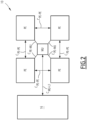
figure 2 shows a part of the CGRA architecture offigure 1 , -
figure 3 shows the functional elements of an example of processing element, -
figure 4 shows the functional elements of an example of memory unit, and -
figure 5 illustrates schematically three scenarios of calculation of an elementary operation. - A coarse-grained reconfigurable array architecture is schematically represented on
figure 1 . - Such architecture is a multicore system adapted to carry out tasks by decomposing the task in subtasks carried out in a parallel way.
- A coarse-grained reconfigurable array architecture is more often named using its abbreviation CGRA, so that the coarse-grained reconfigurable array architecture is named CGRA
architecture 10 hereinafter. - The CGRA
architecture 10 comprises anetwork 12 of processing elements PE, anetwork 14 of memory units MU and amemory controller 20. - The CGRA
architecture 10 is in interaction with a sharedL1 memory 16 and acompiler 18. - The shared
L1 memory 16 is a cache memory placed exterior to the CGRAarchitecture 10, which is shared with a host processor. - The memory units MU are specialized cores to perform loading and storing of data between the shared
L1 memory 16 and theCGRA architecture 10. - The
compiler 18 is dedicated to the CGRAarchitecture 10 and can thus be construed in this example as adedicated compiler 18. Thecompiler 18 is part of the associated toolchain of the CGRAarchitecture 10. - Before describing more precisely the operating of each unit, the geometry of the
networks CGRA architecture 10 is described more precisely in reference tofigure 1 and tofigure 2 , which is an enlarged view of a part offigure 1 . - The
network 12 of processing elements PE is a bidimensional array. -
Such network 12 therefore comprises columns of processing elements PE and rows of processing elements PE. - For the sake of simplicity, the
network 12 of processing elements PE represented onfigure 1 comprises 4 rows and 4 columns. - It can also be defined for the
network 12 of processing elements PE in several directions: West corresponding to left, East corresponding to right, North corresponding to up and South corresponding to down. - Each processing element PE is connected with other processing elements PE by connections CPE-PE through which the processing element PE can exchange data with at least one of the other processing elements PE.
- According to the example of
figure 1 , each connection CPE-PE is a hard-wired communication link. - In the present case, each processing element PE with which a processing element PE can exchange data are the processing elements PE which are adjacent to said processing element PE along the row and the column to which said processing element PE belongs.
- In other words, a processing element PE can exchange data with four neighboring processing elements PE, a first one on the West, a second on the East, a third one on the North and a fourth one on the South.
- For the processing element PE situated at one extremity of the
network 12 and having no direct neighboring processing element PE in a direction, the processing element PE exchanges data with the processing element PE on the other extremity in the same direction. - For instance, the first processing element PE of the first row is adapted to exchange data with the last processing element PE of the first row and is adapted to exchange data with the last processing element PE of the first column.
- The
network 14 of memory units MU is also arranged in a bidimensional array. -
Such network 14 therefore comprises columns of memory units MU and rows of memory units MU. - For the sake of simplicity, the
network 14 of memory units MU represented onfigure 1 comprises 3 rows and 3 columns. - The bidimensional array of memory units MU is spatially shifted with relation to the bidimensional array of processing elements PE.
- Such spatial shift is such that each memory unit MU is placed in a space delimited by four respective processing elements PE.
- This enables that each memory unit MU be at the same distance from four processing elements PE.
- In the present example, each memory unit MU is adapted to communicate with four respective processing elements PE.
- In other words, a memory unit MU can exchange data with four neighboring processing elements PE, a first one on the North-West, a second on the North-East, a third one on the South-West and a fourth one on the South-East.
- Such communication CPE-MU is a hard-wired communication link.
- In addition, each memory unit MU is connected to the shared
L1 memory 16 via a connection CMU-L1. - The existence of the communication channel between the
different network - As apparent from
figure 3 , a processing element PE comprises an IRF, a decoder, an ALU, a control unit and several registers. - The IRF is an instruction register file comprising instructions to be executed by the processing element PE.
- The processing element PE is indeed capable of executing an instruction at each clock cycle.
- The decoder is adapted to convert the instruction in commands for the other blocks of the processing element PE.
- The ALU is an arithmetic logic unit, in which the processing element PE makes a calculation on incoming data to calculate an output data.
- The control unit is adapted to control the flux between the blocks of the processing element PE and notably ensure that the converted instructions be sent to the appropriate block.
- The registers comprise several kind of registers, namely PE-PE registers, PE-MU registers and a register file RF.
- The PE-PE registers are registers intended to broadcast information to all the four neighboring processing elements PE.
- More precisely, in reference to
figure 3 , the N register stores data to be received from the processing element PE situated in the north of the processing element PE, the S register stores data to be received from the processing element PE situated in the south, the E register stores data to be received from the processing element PE situated in the east and the W register stores data to be received from the processing element PE situated in the west. - First indexed register R0 in the register file RF of each processing element PE temporarily stores the output from ALU which is broadcasted to adjacent processing elements PE. Any data which needs to be broadcasted to adjacent processing elements PE is moved to first indexed register R0 in the register file RF by issuing a MOVE instruction in that particular processing element PE.
- The PE-MU registers are intermediate registers between the processing element PE and its neighboring memory units MU.
- There are thus four PE-MU registers in each processing element PE, namely NW, NE, SW, and SE, to receive incoming data from the associated memory unit MU in North-West, North-East, South-West, and South-East directions, respectively.
- The register file RF is a local register file to store temporary data within a processing element PE.
- As apparent from
figure 4 , a memory unit MU comprises an IRF, a decoder, a control unit, an AGU, a LSU and several registers. - The IRF, decoder and control unit are similar to the corresponding block of the processing element PE.
- The AGU is the address generation unit.
- The LSU is the load-store unit.
- The register comprises seven registers: a Tx register, a Rx register, a BR register and 4 PE registers.
- The Tx register is the transmitter register and is meant to send data to the shared
L1 memory 16 for storing. - By issuing a MOVE instruction in the memory unit MU, data stored in the PE registers are moved to said Tx register.
- The sent data is later stored in the shared
L1 memory 16 by issuing a STORE instruction in the memory unit MU. - The Rx register is the receiver register and is meant to receive data from the shared
L1 memory 16 and store the received data. - The memory unit MU loads data from shared
L1 memory 16 into the Rx register by issuing a LOAD instruction. - The BR register is a broadcast register serving to store data to be broadcasted to the neighboring processing elements PE in each direction, respectively North-West, North-East, South-West, and South-East directions, respectively.
- The BR register receives data from the Rx register.
- Each PE register is dedicated to the receiving of data from a respective processing element PE.
- There is thus a NE register to receive data from the north-east processing element PE, a NW register to receive data from the north-west processing element PE, a SW register to receive data from the south-west processing element PE and a SE register to receive data from the south-east processing element PE.
- The
memory controller 20 is adapted to distribute the instructions to the different processing elements PE and memory units MU. - In the present case, the
compiler 18 is used to convert the application to be executed on theCGRA architecture 10 into elementary operations for each processing element PE and memory unit MU. - By definition, an elementary operation is the application of a calculation on at least one input data to calculate an output data.
- A task is made of many elementary operations.
- An elementary operation is carried out by executing at least one input data exchange instruction, a calculation instruction and an output data exchange instruction.
- The
compiler 18 is further adapted to allocate each instruction to the appropriate processing element PE or memory unit MU. - For instance, each processing element PE or memory unit MU implied in the execution of the operation should ideally be very close.
- In operation, the
memory controller 20 is adapted to fetch the input data exchange instructions, the calculation instructions and the output data exchange instructions stored in a separate memory. - More precisely, the instructions for each processing unit PE and memory unit MU generated from the
compiler 18 are stored in a separate memory, which is accessed by thememory controller 20 and distributed to each processing unit PE and memory unit MU respectively. - It can here be noted that these operations of fetching instructions and distributing them is carried out before the beginning of the execution of the
CGRA architecture 10. - The
memory controller 20 sends each calculation instruction and output data exchange to the appropriate processing element PE to execute said calculation instruction and said output data exchange instruction and thememory controller 20 also sends each input data exchange instruction to the appropriate MU to execute said input data exchange instruction before the execution begins in theCGRA architecture 10. - In other words, each processing element PE is dedicated to perform arithmetic and logic calculations and not to manage the input data movements.
- In addition, the processing elements PE and the memory units MU operate separately by executing their own instruction routines.
- Such operation correspond to a method for carrying out tasks with the
CGRA architecture 10, said method comprising a first phase carried out by thecompiler 18 and a second phase carried out by thememory controller 20. - The first phase comprises a step of converting the tasks to be carried out by the coarse-grained reconfigurable array architecture into elementary operations and a step of allocating each instruction to the appropriate processing element or memory unit.
- The second comprises fetching the input data exchange instructions, the calculation instructions and the output data exchange instructions, a first step of sending each calculation instruction and output data exchange to the appropriate processing element PE to execute said calculation instruction and said output data exchange instruction, and a second step of sending each input data exchange instruction to the appropriate memory unit MU to execute said input data exchange instruction, the sending steps being carried out by the
memory controller 20. - The synchronization between the instructions and their execution by the processing elements PE and the memory units MU is ensured at the level of compilation by the
compiler 18. The scheduling of the operations is performed separately by thecompiler 18. - This enables to speed up the execution of the elementary operations, as will be shown in reference to
figure 5 . -
Figure 5 illustrates the action carried out by a memory unit MU and the processing unit for three different cases. - The first case corresponds to the case where the processing unit and the memory unit MU are fused into a single module.
- In such case, the processing element PE also manages the input data movements.
- Therefore, at a predefined time named n, the processing element PE receives instructions to carry out the elementary operation A[i] = B[i] * C[i], where B[i] and C[i] are the data to be loaded from memory, and A[i] is the result to be stored in memory which is obtained from the multiplication of B[i] and C[i].
- Each time is here timestamped by a clock unit, which is not represented.
- The execution of the received instructions leads to the following actions:
- the processing element PE requests loading of B[i] to shared
L1 memory 16 at time n, - the processing element PE receives B[i] at
time n+ 1, - the processing element PE requests loading of C[i] to shared
L1 memory 16 attime n+ 2, - the processing element PE receives C[i] at
time n+ 3, - the processing element PE carries out B[i] * C[i] at
time n+ 4, - the processing element PE sends the result A[i] at time n+5 for storing in shared
L1 memory 16, and - the result A[i] is stored in the shared
L1 memory 16 attime n+ 6. - This means that 7 clock cycles are necessary to carry out the element operation A[i] = B[i] * C[i], given that no memory stalls occur during the execution.
- By comparison, the second case and third case illustrates the advantages provided by the use of the
CGRA architecture 10 as presently described. -
Case 2 corresponds to a decoupled scenario in which at least one processing element PE and one memory unit MU are separated and forms a group. - In other words, in this scenario, the input data exchange instructions are sent to the memory unit MU so that the memory unit MU has provided the input data to the processing element PE before the predefined time n.
- The execution of the received instructions leads to the following actions:
- the memory unit MU sends request to shared
L1 memory 16 to load B[i] at time n-4, - the memory unit MU receives B[i] from shared
L1 memory 16 at time n-3, and B[i] is immediately available to the processing element PE, - the memory unit MU requests to shared
L1 memory 16 to load C[i] at time n-2, - the memory unit MU receives C[i] from shared
L1 memory 16 at time n-1, and C[i] is immediately available to the processing unit PE , - the PE carries out B[i] * C[i] at time n, and result A[i] is immediately available to the memory unit MU,
- the memory unit MU sends the result A[i] at time n+1 for storing in shared
L1 memory 16, and - the result A[i] is stored in the shared
L1 memory 16 attime n+ 2. - The number of clock cycles necessary to carry out the elementary operation is thus the same with relation to
case 1 but the result is available 4 clock cycles before at time n+2 and not attime n+ 6. -
Case 3 corresponds to an enhanced execution scenario wherein several memory units MU are used, namely a first memory unit MU1 and a second memory unit MU2. - In such case, the
memory controller 20 sends respective input data exchange instructions to a respective memory unit MU connected to the processing element PE, the input data exchange instructions being sent to each memory unit MU so that the memory unit MU has provided the data to the processing element PE before the predefined time n. - It is also assumed that the memory units MU provide simultaneously their respective input data to the processing element PE.
- The execution of the received instructions leads to the following actions:
- the first memory unit MU1 requests loading of B[i] from the shared
L1 memory 16 at time n-2, - the first memory unit MU1 receives B[i] from the shared
L1 memory 16 at time n-1, and B[i] is immediately available to the processing element PE, - the second memory unit MU2 requests loading of C[i] from the shared
L1 memory 16 at time n-2, - the second memory unit MU2 receives C[i] from the shared
L1 memory 16 at time n-1, and C[i] is immediately available to PE, - the processing element PE carries out B[i] * C[i] at time n, and result A[i] is immediately available to both the first memory unit MU1 and the second memory unit MU2,
- depending on the scheduling during the compilation time, either the first memory unit MU1 or the second memory unit MU2 sends the result A[i] at time n+1 for storing in the shared
L1 memory 16, and - the result A[i] is stored in the shared
L1 memory 16 attime n+ 2. - In this case, the total execution time is reduced to 5 clock cycles thanks to the fact that each data loading is performed in parallel, and sharing of data between processing element PE and the memory units MU1 and MU2 is carried out as soon as data is available in the either memory units MU1/MU2 or the processing element PE.
- The Overall Speedup provided by the
case 3 with relation tocase 1 can be obtained by applying an Amdahl's law. - The Overall Speedup therefore fulfills the following relation:

- OS designates the overall speedup,
- FE designates the fraction enhanced equal to the ratio of the time that can be enhanced over the total time, and
- SE designates the speedup enhanced equal to the ratio of the time that can be enhanced over the time after enhancement.
- In the present case, the time that cannot be enhanced is equal to 3 clock cycles (the instruction carried out by the processing element PE and following instruction carried out by the memory unit MU) and the time that can be enhanced is equal to 4 clock cycles (the instructions carried out by the memory units MU, i.e., the instructions scheduled before the arithmetic operation to be carried out by the processing element PE). This leads to a total time of 7 clock cycles.
- After enhancement, instead of 4 clock cycles, 2 clock cycles are needed.
- This leads to the following values for FE and SE:


- By applying this to the calculation of the overall speedup OS:

- Such value is to be compared with the maximum speedup that can be achieved with an enhanced execution setup in this case.
- Such maximum is obtained by applying Amdahl's Law for Absolute Limits. The corresponding mathematical relations is as follows:

- The acceleration provided in the execution of the tasks in the third scenario is thus very interesting.
- The
present CGRA architecture 10 therefore aids in accelerating a given carrying out of a task in a manycore architecture. - Such gain is obtained by dedicating elements to perform only memory operations (namely LOAD and STORE) and the other elements to execute arithmetic and logic operations while getting data from the former elements.
- This implies separating the calculation instructions from the input data instructions and creating an optimal register map scheme between the processing elements PE and the memory units MU.
- The obtained gain is also increased by the spatial arrangement of the
networks CGRA architecture 10, which ensures that the distance between the processing elements PE and the memory units MU implied in an elementary operation is the shortest possible. - Other embodiments of the
present CGRA architecture 10 may be considered. - For instance, it may be considered other geometries for the
networks - As a specific example, it may be advantageous that there is same type of connection between the processing elements PE, specially the processing elements PE that are situated at extremities could avoid the longest connections in the
CGRA architecture 10. This provides a mesh torus type of switchless interconnect network in thenetwork 12 of processing elements PE. - The architecture to consider here will share the property according to which each processing element PE is connected with at least one memory unit MU by connections through which the memory unit MU can exchange data with the processing element PE.
- When appropriate, it can also be considered to separate the tasks among group of processing units.
- For instance, the
network 12 of processing elements PE could be soft clustered (software-based clustering, performed at the compile time while scheduling the instructions for each processing units) to perform two separate tasks, i.e., one cluster of the network 12 (thereby forming a sub-array of processing elements PE) is devoted to carry out one task while the other cluster of thenetwork 12 is devoted to carry out another task. Such configuration is notably adapted for the case of two applications. - Another example is the case of convolution in which the same kernel is applied to each part of an image. In such case, it is advantageous to operate the kernel in parallel, each group of processing elements PE applying the same kernel to different part of the image.
- The two previous examples can be combined in presence of several applications consisting in applying a respective kernel. The
network - The scheduling process of the
compiler 18 can be improved. - In particular, in the conversion process of application into operations by the
compiler 18, thecompiler 18 eliminates redundant operations. - This notably avoids issuing extra MOVE operations to move data among them.
- Data hazards, such as Read after Write (RAW), Write after Read (WAR), and Write after Write (WAW), may also be avoided by either inserting stalls (no-operation instructions) or code reordering.
- Another optimization that can be carried out during the conversion process is modifying the execution of some steps.
- For instance, in case the operation is an accumulation, it can be considered temporarily storing the accumulations in a local register. This results in avoiding useless STORE instructions to perform memory access for only the final result.
- In each embodiment, the coarse-grained reconfigurable array architecture has an improved execution time.
Claims (10)
- Coarse-grained reconfigurable array architecture (10) adapted to carry out tasks, the coarse-grained reconfigurable array architecture (10) comprising:- a network (12) of processing elements (PE), each processing element (PE) being connected with other processing elements (PE) by connections (CPE-PE) through which the processing element (PE) can exchange data with at least one of the other processing elements (PE),- a network (14) of memory units (MU), each memory unit (MU) being adapted to exchange data with several processing elements (PE), each processing element (PE) being connected with at least one memory unit (MU) by connections (CPE-MU) through which the memory unit (MU) can exchange data with the processing element (PE),- a compiler (18) adapted to convert the tasks to be carried out by the coarse-grained reconfigurable array architecture (10) into elementary operations,each elementary operation consisting in applying a calculation on at least one input data to calculate an output data by executing at least one input data exchange instruction, a calculation instruction and an output data exchange instruction,the compiler (18) being further adapted to allocate each instruction to the appropriate processing element (PE) or memory unit (MU),- a memory controller (20) adapted to fetch the input data exchange instructions, the calculation instructions and the output data exchange instructions,the memory controller (20) being further adapted to send each calculation instruction and output data exchange to the appropriate processing element (PE) to execute said calculation instruction and said output data exchange instruction andthe memory controller (20) being further adapted to send each input data exchange instruction to the appropriate memory unit (MU) to execute said input data exchange instruction.
- Coarse-grained reconfigurable array architecture according to claim 1, wherein, for each elementary instruction,the memory controller (20) sends each calculation instruction and output data exchange instruction to a processing element (PE) to execute said calculation instruction and output data exchange instruction at a predefined time,the memory controller (20) further sends each input data exchange instruction to a memory unit (MU) connected to said processing element (PE), the input data exchange instructions being sent to the memory unit (MU) so that the memory unit (MU) has provided the input data to the processing element (PE) before the predefined time.
- Coarse-grained reconfigurable array architecture according to claim 1, wherein, for each elementary instruction,the memory controller (20) sends each calculation instruction and output data exchange instruction to a processing element (PE) to execute said calculation instruction and output data exchange instruction at a predefined time,the memory controller (20) further sends a respective input data exchange instruction to a respective memory unit (MU) connected to said processing element (PE), the input data exchange instructions being sent to each memory unit (MU) so that the memory unit (MU) has provided the data to the processing element (PE) before the predefined time.
- Coarse-grained reconfigurable array architecture according to claim 3, wherein the memory units (MU) provide simultaneously the data to the processing element (PE).
- Coarse-grained reconfigurable array architecture according to any one of claims 1 to 4, wherein the network (12) of processing elements (PE) is arranged in a bidimensional array.
- Coarse-grained reconfigurable array architecture according to claim 5, wherein the network (12) of processing elements (PE) comprises columns of processing elements (PE) and rows of processing elements (PE) and wherein, for each processing element (PE), the processing elements (PE) with which a processing element (PE) can exchange data are the processing elements (PE) which are adjacent to said processing element (PE) along the row and the column to which said processing element (PE) belongs.
- Coarse-grained reconfigurable array architecture according to any one of the previous claims 1 to 6, wherein the network (14) of memory units (MU) is arranged in a bidimensional array.
- Coarse-grained reconfigurable array architecture according to claim 7, wherein the bidimensional array of memory units (MU) comprises columns of memory units (MU) and rows of memory units (MU), each memory unit (MU) being placed in a space delimited by four respective processing elements (PE).
- Coarse-grained reconfigurable array architecture according to any one of claims 1 to 8, wherein each memory unit (MU) is adapted to communicate with four respective processing elements (PE).
- Method for carrying out tasks with a coarse-grained reconfigurable array architecture (10), the coarse-grained reconfigurable array architecture (10) comprising:- a network (12) of processing elements (PE), each processing element (PE) being connected with other processing elements (PE) by connections (CPE-PE) through which the processing element (PE) can exchange data with at least one of the other processing elements (PE),- a network (14) of memory units (MU), each memory unit (MU) being adapted to exchange data with several processing elements (PE), each processing element (PE) being connected with at least one memory unit (MU) by connections (CPE-MU) through which the memory unit (MU) can exchange data with the processing element (PE),- a compiler (18), and- a memory controller (20),the method comprising the steps of:- converting the tasks to be carried out by the coarse-grained reconfigurable array architecture (10) into elementary operations,each elementary operation consisting in applying a calculation on at least one input data to calculate an output data by executing at least one input data exchange instruction, a calculation instruction and an output data exchange instruction,- allocating each instruction to the appropriate processing element (PE) or memory unit (MU),- fetching the input data exchange instructions, the calculation instructions and the output data exchange instructions, the fetching step being carried out by the memory controller (20),- sending each calculation instruction and output data exchange to the appropriate processing element (PE) to execute said calculation instruction and said output data exchange instruction, and- sending each input data exchange instruction to the appropriate memory unit (MU) to execute said input data exchange instruction, the sending steps being carried out by the memory controller (20).
Priority Applications (2)
| Application Number | Priority Date | Filing Date | Title |
|---|---|---|---|
| EP23307090.3A EP4564185A1 (en) | 2023-11-29 | 2023-11-29 | Coarse-grained reconfigurable array architecture and associated method |
| EP24216210.5A EP4564187A1 (en) | 2023-11-29 | 2024-11-28 | Coarse-grained reconfigurable array architecture and associated method |
Applications Claiming Priority (1)
| Application Number | Priority Date | Filing Date | Title |
|---|---|---|---|
| EP23307090.3A EP4564185A1 (en) | 2023-11-29 | 2023-11-29 | Coarse-grained reconfigurable array architecture and associated method |
Publications (1)
| Publication Number | Publication Date |
|---|---|
| EP4564185A1 true EP4564185A1 (en) | 2025-06-04 |
Family
ID=89854660
Family Applications (2)
| Application Number | Title | Priority Date | Filing Date |
|---|---|---|---|
| EP23307090.3A Withdrawn EP4564185A1 (en) | 2023-11-29 | 2023-11-29 | Coarse-grained reconfigurable array architecture and associated method |
| EP24216210.5A Pending EP4564187A1 (en) | 2023-11-29 | 2024-11-28 | Coarse-grained reconfigurable array architecture and associated method |
Family Applications After (1)
| Application Number | Title | Priority Date | Filing Date |
|---|---|---|---|
| EP24216210.5A Pending EP4564187A1 (en) | 2023-11-29 | 2024-11-28 | Coarse-grained reconfigurable array architecture and associated method |
Country Status (1)
| Country | Link |
|---|---|
| EP (2) | EP4564185A1 (en) |
Citations (2)
| Publication number | Priority date | Publication date | Assignee | Title |
|---|---|---|---|---|
| US20160328231A1 (en) * | 2013-05-24 | 2016-11-10 | Coherent Logix, Incorporated | Memory-network processor with programmable optimizations |
| US20220261364A1 (en) * | 2021-02-12 | 2022-08-18 | SambaNova Systems, Inc. | Compile Time Instrumentation of Data Flow Graphs |
-
2023
- 2023-11-29 EP EP23307090.3A patent/EP4564185A1/en not_active Withdrawn
-
2024
- 2024-11-28 EP EP24216210.5A patent/EP4564187A1/en active Pending
Patent Citations (3)
| Publication number | Priority date | Publication date | Assignee | Title |
|---|---|---|---|---|
| US20160328231A1 (en) * | 2013-05-24 | 2016-11-10 | Coherent Logix, Incorporated | Memory-network processor with programmable optimizations |
| US11544072B2 (en) | 2013-05-24 | 2023-01-03 | Coherent Logix, Inc. | Memory-network processor with programmable optimizations |
| US20220261364A1 (en) * | 2021-02-12 | 2022-08-18 | SambaNova Systems, Inc. | Compile Time Instrumentation of Data Flow Graphs |
Non-Patent Citations (2)
| Title |
|---|
| PRABHAKAR RAGHU ET AL: "Plasticine: A reconfigurable architecture for parallel patterns", 2017 ACM/IEEE 44TH ANNUAL INTERNATIONAL SYMPOSIUM ON COMPUTER ARCHITECTURE (ISCA), ACM, 24 June 2017 (2017-06-24), pages 389 - 402, XP033268533, DOI: 10.1145/3079856.3080256 * |
| ZHANG YAQI ET AL: "SARA: Scaling a Reconfigurable Dataflow Accelerator", 2021 ACM/IEEE 48TH ANNUAL INTERNATIONAL SYMPOSIUM ON COMPUTER ARCHITECTURE (ISCA), IEEE, 14 June 2021 (2021-06-14), pages 1041 - 1054, XP033951969, DOI: 10.1109/ISCA52012.2021.00085 * |
Also Published As
| Publication number | Publication date |
|---|---|
| EP4564187A1 (en) | 2025-06-04 |
Similar Documents
| Publication | Publication Date | Title |
|---|---|---|
| US6219775B1 (en) | Massively parallel computer including auxiliary vector processor | |
| US7574466B2 (en) | Method for finding global extrema of a set of shorts distributed across an array of parallel processing elements | |
| CN107679621A (en) | Artificial Neural Network Processing Device | |
| CN107704922A (en) | Artificial neural network processing unit | |
| GB2458554A (en) | Coalescing memory accesses from multiple threads in a parallel processing system | |
| JP2001523023A (en) | Method and apparatus for efficient synchronous MIMD operation using iVLIW inter-PE communication | |
| CN111047036A (en) | Neural network processor, chip and electronic equipment | |
| EP2796991A2 (en) | Processor for batch thread processing, batch thread processing method using the same, and code generation apparatus for batch thread processing | |
| JP2023509813A (en) | SIMT command processing method and device | |
| EP4432210A1 (en) | Data processing method and apparatus, electronic device, and computer-readable storage medium | |
| EP0295646B1 (en) | Arithmetic operation processing apparatus of the parallel processing type and compiler which is used in this apparatus | |
| EP4455876A1 (en) | Task processing method, chip, multi-chip module, electronic device, and storage medium | |
| JP6493088B2 (en) | Arithmetic processing device and control method of arithmetic processing device | |
| US9760969B2 (en) | Graphic processing system and method thereof | |
| US20080209165A1 (en) | Simd microprocessor, image processing apparatus including same, and image processing method used therein | |
| EP4564185A1 (en) | Coarse-grained reconfigurable array architecture and associated method | |
| WO2016024508A1 (en) | Multiprocessor device | |
| EP2254057B1 (en) | Simd processor array system and data transfer method thereof | |
| US8024549B2 (en) | Two-dimensional processor array of processing elements | |
| EP0729616B1 (en) | A data processing system comprising data processing units and an expander | |
| CN116775283A (en) | GPGPU resource allocation management method and system | |
| JP5708634B2 (en) | SIMD processor | |
| US11940940B2 (en) | External exchange connectivity | |
| US20250298773A1 (en) | 3d dataflow architecture for a computing device | |
| WO2011151000A9 (en) | Method and device for data processing |
Legal Events
| Date | Code | Title | Description |
|---|---|---|---|
| PUAI | Public reference made under article 153(3) epc to a published international application that has entered the european phase |
Free format text: ORIGINAL CODE: 0009012 |
|
| STAA | Information on the status of an ep patent application or granted ep patent |
Free format text: STATUS: REQUEST FOR EXAMINATION WAS MADE |
|
| 17P | Request for examination filed |
Effective date: 20231130 |
|
| AK | Designated contracting states |
Kind code of ref document: A1 Designated state(s): AL AT BE BG CH CY CZ DE DK EE ES FI FR GB GR HR HU IE IS IT LI LT LU LV MC ME MK MT NL NO PL PT RO RS SE SI SK SM TR |
|
| STAA | Information on the status of an ep patent application or granted ep patent |
Free format text: STATUS: THE APPLICATION IS DEEMED TO BE WITHDRAWN |
|
| 18D | Application deemed to be withdrawn |
Effective date: 20251205 |