EP4561296A2 - Complementary fet device and control method thereof - Google Patents
Complementary fet device and control method thereof Download PDFInfo
- Publication number
- EP4561296A2 EP4561296A2 EP24211343.9A EP24211343A EP4561296A2 EP 4561296 A2 EP4561296 A2 EP 4561296A2 EP 24211343 A EP24211343 A EP 24211343A EP 4561296 A2 EP4561296 A2 EP 4561296A2
- Authority
- EP
- European Patent Office
- Prior art keywords
- channel layer
- layer
- gate
- source
- drain region
- Prior art date
- Legal status (The legal status is an assumption and is not a legal conclusion. Google has not performed a legal analysis and makes no representation as to the accuracy of the status listed.)
- Pending
Links
Images


















Classifications
-
- H—ELECTRICITY
- H10—SEMICONDUCTOR DEVICES; ELECTRIC SOLID-STATE DEVICES NOT OTHERWISE PROVIDED FOR
- H10D—INORGANIC ELECTRIC SEMICONDUCTOR DEVICES
- H10D88/00—Three-dimensional [3D] integrated devices
-
- B—PERFORMING OPERATIONS; TRANSPORTING
- B82—NANOTECHNOLOGY
- B82Y—SPECIFIC USES OR APPLICATIONS OF NANOSTRUCTURES; MEASUREMENT OR ANALYSIS OF NANOSTRUCTURES; MANUFACTURE OR TREATMENT OF NANOSTRUCTURES
- B82Y40/00—Manufacture or treatment of nanostructures
-
- H—ELECTRICITY
- H10—SEMICONDUCTOR DEVICES; ELECTRIC SOLID-STATE DEVICES NOT OTHERWISE PROVIDED FOR
- H10D—INORGANIC ELECTRIC SEMICONDUCTOR DEVICES
- H10D30/00—Field-effect transistors [FET]
- H10D30/01—Manufacture or treatment
- H10D30/014—Manufacture or treatment of FETs having zero-dimensional [0D] or one-dimensional [1D] channels, e.g. quantum wire FETs, single-electron transistors [SET] or Coulomb blockade transistors
-
- H—ELECTRICITY
- H10—SEMICONDUCTOR DEVICES; ELECTRIC SOLID-STATE DEVICES NOT OTHERWISE PROVIDED FOR
- H10D—INORGANIC ELECTRIC SEMICONDUCTOR DEVICES
- H10D30/00—Field-effect transistors [FET]
- H10D30/01—Manufacture or treatment
- H10D30/019—Manufacture or treatment of FETs having stacked nanowire, nanosheet or nanoribbon channels
- H10D30/0195—Manufacture or treatment of FETs having stacked nanowire, nanosheet or nanoribbon channels forming inner spacers between adjacent channels, e.g. changing their shapes or sizes
-
- H—ELECTRICITY
- H10—SEMICONDUCTOR DEVICES; ELECTRIC SOLID-STATE DEVICES NOT OTHERWISE PROVIDED FOR
- H10D—INORGANIC ELECTRIC SEMICONDUCTOR DEVICES
- H10D30/00—Field-effect transistors [FET]
- H10D30/40—FETs having zero-dimensional [0D], one-dimensional [1D] or two-dimensional [2D] charge carrier gas channels
- H10D30/43—FETs having zero-dimensional [0D], one-dimensional [1D] or two-dimensional [2D] charge carrier gas channels having one-dimensional [1D] charge carrier gas channels, e.g. quantum wire FETs or transistors having 1D quantum-confined channels
-
- H—ELECTRICITY
- H10—SEMICONDUCTOR DEVICES; ELECTRIC SOLID-STATE DEVICES NOT OTHERWISE PROVIDED FOR
- H10D—INORGANIC ELECTRIC SEMICONDUCTOR DEVICES
- H10D30/00—Field-effect transistors [FET]
- H10D30/501—FETs having stacked nanowire, nanosheet or nanoribbon channels
- H10D30/507—FETs having stacked nanowire, nanosheet or nanoribbon channels characterised by inner spacers between adjacent channels
- H10D30/508—FETs having stacked nanowire, nanosheet or nanoribbon channels characterised by inner spacers between adjacent channels characterised by the relative sizes, shapes or dispositions of the inner spacers
-
- H—ELECTRICITY
- H10—SEMICONDUCTOR DEVICES; ELECTRIC SOLID-STATE DEVICES NOT OTHERWISE PROVIDED FOR
- H10D—INORGANIC ELECTRIC SEMICONDUCTOR DEVICES
- H10D30/00—Field-effect transistors [FET]
- H10D30/60—Insulated-gate field-effect transistors [IGFET]
- H10D30/67—Thin-film transistors [TFT]
- H10D30/6729—Thin-film transistors [TFT] characterised by the electrodes
- H10D30/673—Thin-film transistors [TFT] characterised by the electrodes characterised by the shapes, relative sizes or dispositions of the gate electrodes
- H10D30/6735—Thin-film transistors [TFT] characterised by the electrodes characterised by the shapes, relative sizes or dispositions of the gate electrodes having gates fully surrounding the channels, e.g. gate-all-around
-
- H—ELECTRICITY
- H10—SEMICONDUCTOR DEVICES; ELECTRIC SOLID-STATE DEVICES NOT OTHERWISE PROVIDED FOR
- H10D—INORGANIC ELECTRIC SEMICONDUCTOR DEVICES
- H10D30/00—Field-effect transistors [FET]
- H10D30/60—Insulated-gate field-effect transistors [IGFET]
- H10D30/67—Thin-film transistors [TFT]
- H10D30/6757—Thin-film transistors [TFT] characterised by the structure of the channel, e.g. transverse or longitudinal shape or doping profile
-
- H—ELECTRICITY
- H10—SEMICONDUCTOR DEVICES; ELECTRIC SOLID-STATE DEVICES NOT OTHERWISE PROVIDED FOR
- H10D—INORGANIC ELECTRIC SEMICONDUCTOR DEVICES
- H10D62/00—Semiconductor bodies, or regions thereof, of devices having potential barriers
- H10D62/10—Shapes, relative sizes or dispositions of the regions of the semiconductor bodies; Shapes of the semiconductor bodies
- H10D62/117—Shapes of semiconductor bodies
- H10D62/118—Nanostructure semiconductor bodies
- H10D62/119—Nanowire, nanosheet or nanotube semiconductor bodies
- H10D62/121—Nanowire, nanosheet or nanotube semiconductor bodies oriented parallel to substrates
-
- H—ELECTRICITY
- H10—SEMICONDUCTOR DEVICES; ELECTRIC SOLID-STATE DEVICES NOT OTHERWISE PROVIDED FOR
- H10D—INORGANIC ELECTRIC SEMICONDUCTOR DEVICES
- H10D64/00—Electrodes of devices having potential barriers
- H10D64/01—Manufacture or treatment
- H10D64/017—Manufacture or treatment using dummy gates in processes wherein at least parts of the final gates are self-aligned to the dummy gates, i.e. replacement gate processes
-
- H—ELECTRICITY
- H10—SEMICONDUCTOR DEVICES; ELECTRIC SOLID-STATE DEVICES NOT OTHERWISE PROVIDED FOR
- H10D—INORGANIC ELECTRIC SEMICONDUCTOR DEVICES
- H10D64/00—Electrodes of devices having potential barriers
- H10D64/01—Manufacture or treatment
- H10D64/018—Spacers formed inside holes at the prospective gate locations, e.g. holes left by removing dummy gates
-
- H—ELECTRICITY
- H10—SEMICONDUCTOR DEVICES; ELECTRIC SOLID-STATE DEVICES NOT OTHERWISE PROVIDED FOR
- H10D—INORGANIC ELECTRIC SEMICONDUCTOR DEVICES
- H10D84/00—Integrated devices formed in or on semiconductor substrates that comprise only semiconducting layers, e.g. on Si wafers or on GaAs-on-Si wafers
- H10D84/01—Manufacture or treatment
- H10D84/0123—Integrating together multiple components covered by H10D12/00 or H10D30/00, e.g. integrating multiple IGBTs
- H10D84/0126—Integrating together multiple components covered by H10D12/00 or H10D30/00, e.g. integrating multiple IGBTs the components including insulated gates, e.g. IGFETs
- H10D84/0128—Manufacturing their channels
-
- H—ELECTRICITY
- H10—SEMICONDUCTOR DEVICES; ELECTRIC SOLID-STATE DEVICES NOT OTHERWISE PROVIDED FOR
- H10D—INORGANIC ELECTRIC SEMICONDUCTOR DEVICES
- H10D84/00—Integrated devices formed in or on semiconductor substrates that comprise only semiconducting layers, e.g. on Si wafers or on GaAs-on-Si wafers
- H10D84/01—Manufacture or treatment
- H10D84/0123—Integrating together multiple components covered by H10D12/00 or H10D30/00, e.g. integrating multiple IGBTs
- H10D84/0126—Integrating together multiple components covered by H10D12/00 or H10D30/00, e.g. integrating multiple IGBTs the components including insulated gates, e.g. IGFETs
- H10D84/0165—Integrating together multiple components covered by H10D12/00 or H10D30/00, e.g. integrating multiple IGBTs the components including insulated gates, e.g. IGFETs the components including complementary IGFETs, e.g. CMOS devices
- H10D84/0167—Manufacturing their channels
-
- H—ELECTRICITY
- H10—SEMICONDUCTOR DEVICES; ELECTRIC SOLID-STATE DEVICES NOT OTHERWISE PROVIDED FOR
- H10D—INORGANIC ELECTRIC SEMICONDUCTOR DEVICES
- H10D84/00—Integrated devices formed in or on semiconductor substrates that comprise only semiconducting layers, e.g. on Si wafers or on GaAs-on-Si wafers
- H10D84/01—Manufacture or treatment
- H10D84/0123—Integrating together multiple components covered by H10D12/00 or H10D30/00, e.g. integrating multiple IGBTs
- H10D84/0126—Integrating together multiple components covered by H10D12/00 or H10D30/00, e.g. integrating multiple IGBTs the components including insulated gates, e.g. IGFETs
- H10D84/0165—Integrating together multiple components covered by H10D12/00 or H10D30/00, e.g. integrating multiple IGBTs the components including insulated gates, e.g. IGFETs the components including complementary IGFETs, e.g. CMOS devices
- H10D84/0172—Manufacturing their gate conductors
- H10D84/0177—Manufacturing their gate conductors the gate conductors having different materials or different implants
-
- H—ELECTRICITY
- H10—SEMICONDUCTOR DEVICES; ELECTRIC SOLID-STATE DEVICES NOT OTHERWISE PROVIDED FOR
- H10D—INORGANIC ELECTRIC SEMICONDUCTOR DEVICES
- H10D84/00—Integrated devices formed in or on semiconductor substrates that comprise only semiconducting layers, e.g. on Si wafers or on GaAs-on-Si wafers
- H10D84/01—Manufacture or treatment
- H10D84/0123—Integrating together multiple components covered by H10D12/00 or H10D30/00, e.g. integrating multiple IGBTs
- H10D84/0126—Integrating together multiple components covered by H10D12/00 or H10D30/00, e.g. integrating multiple IGBTs the components including insulated gates, e.g. IGFETs
- H10D84/0165—Integrating together multiple components covered by H10D12/00 or H10D30/00, e.g. integrating multiple IGBTs the components including insulated gates, e.g. IGFETs the components including complementary IGFETs, e.g. CMOS devices
- H10D84/0184—Manufacturing their gate sidewall spacers
-
- H—ELECTRICITY
- H10—SEMICONDUCTOR DEVICES; ELECTRIC SOLID-STATE DEVICES NOT OTHERWISE PROVIDED FOR
- H10D—INORGANIC ELECTRIC SEMICONDUCTOR DEVICES
- H10D84/00—Integrated devices formed in or on semiconductor substrates that comprise only semiconducting layers, e.g. on Si wafers or on GaAs-on-Si wafers
- H10D84/01—Manufacture or treatment
- H10D84/0123—Integrating together multiple components covered by H10D12/00 or H10D30/00, e.g. integrating multiple IGBTs
- H10D84/0126—Integrating together multiple components covered by H10D12/00 or H10D30/00, e.g. integrating multiple IGBTs the components including insulated gates, e.g. IGFETs
- H10D84/0165—Integrating together multiple components covered by H10D12/00 or H10D30/00, e.g. integrating multiple IGBTs the components including insulated gates, e.g. IGFETs the components including complementary IGFETs, e.g. CMOS devices
- H10D84/0188—Manufacturing their isolation regions
-
- H—ELECTRICITY
- H10—SEMICONDUCTOR DEVICES; ELECTRIC SOLID-STATE DEVICES NOT OTHERWISE PROVIDED FOR
- H10D—INORGANIC ELECTRIC SEMICONDUCTOR DEVICES
- H10D84/00—Integrated devices formed in or on semiconductor substrates that comprise only semiconducting layers, e.g. on Si wafers or on GaAs-on-Si wafers
- H10D84/01—Manufacture or treatment
- H10D84/02—Manufacture or treatment characterised by using material-based technologies
- H10D84/03—Manufacture or treatment characterised by using material-based technologies using Group IV technology, e.g. silicon technology or silicon-carbide [SiC] technology
- H10D84/038—Manufacture or treatment characterised by using material-based technologies using Group IV technology, e.g. silicon technology or silicon-carbide [SiC] technology using silicon technology, e.g. SiGe
-
- H—ELECTRICITY
- H10—SEMICONDUCTOR DEVICES; ELECTRIC SOLID-STATE DEVICES NOT OTHERWISE PROVIDED FOR
- H10D—INORGANIC ELECTRIC SEMICONDUCTOR DEVICES
- H10D84/00—Integrated devices formed in or on semiconductor substrates that comprise only semiconducting layers, e.g. on Si wafers or on GaAs-on-Si wafers
- H10D84/80—Integrated devices formed in or on semiconductor substrates that comprise only semiconducting layers, e.g. on Si wafers or on GaAs-on-Si wafers characterised by the integration of at least one component covered by groups H10D12/00 or H10D30/00, e.g. integration of IGFETs
- H10D84/82—Integrated devices formed in or on semiconductor substrates that comprise only semiconducting layers, e.g. on Si wafers or on GaAs-on-Si wafers characterised by the integration of at least one component covered by groups H10D12/00 or H10D30/00, e.g. integration of IGFETs of only field-effect components
- H10D84/83—Integrated devices formed in or on semiconductor substrates that comprise only semiconducting layers, e.g. on Si wafers or on GaAs-on-Si wafers characterised by the integration of at least one component covered by groups H10D12/00 or H10D30/00, e.g. integration of IGFETs of only field-effect components of only insulated-gate FETs [IGFET]
- H10D84/85—Complementary IGFETs, e.g. CMOS
-
- H—ELECTRICITY
- H10—SEMICONDUCTOR DEVICES; ELECTRIC SOLID-STATE DEVICES NOT OTHERWISE PROVIDED FOR
- H10D—INORGANIC ELECTRIC SEMICONDUCTOR DEVICES
- H10D84/00—Integrated devices formed in or on semiconductor substrates that comprise only semiconducting layers, e.g. on Si wafers or on GaAs-on-Si wafers
- H10D84/80—Integrated devices formed in or on semiconductor substrates that comprise only semiconducting layers, e.g. on Si wafers or on GaAs-on-Si wafers characterised by the integration of at least one component covered by groups H10D12/00 or H10D30/00, e.g. integration of IGFETs
- H10D84/82—Integrated devices formed in or on semiconductor substrates that comprise only semiconducting layers, e.g. on Si wafers or on GaAs-on-Si wafers characterised by the integration of at least one component covered by groups H10D12/00 or H10D30/00, e.g. integration of IGFETs of only field-effect components
- H10D84/83—Integrated devices formed in or on semiconductor substrates that comprise only semiconducting layers, e.g. on Si wafers or on GaAs-on-Si wafers characterised by the integration of at least one component covered by groups H10D12/00 or H10D30/00, e.g. integration of IGFETs of only field-effect components of only insulated-gate FETs [IGFET]
- H10D84/85—Complementary IGFETs, e.g. CMOS
- H10D84/851—Complementary IGFETs, e.g. CMOS comprising IGFETs having stacked nanowire, nanosheet or nanoribbon channels
-
- H—ELECTRICITY
- H10—SEMICONDUCTOR DEVICES; ELECTRIC SOLID-STATE DEVICES NOT OTHERWISE PROVIDED FOR
- H10D—INORGANIC ELECTRIC SEMICONDUCTOR DEVICES
- H10D88/00—Three-dimensional [3D] integrated devices
- H10D88/01—Manufacture or treatment
-
- B—PERFORMING OPERATIONS; TRANSPORTING
- B82—NANOTECHNOLOGY
- B82Y—SPECIFIC USES OR APPLICATIONS OF NANOSTRUCTURES; MEASUREMENT OR ANALYSIS OF NANOSTRUCTURES; MANUFACTURE OR TREATMENT OF NANOSTRUCTURES
- B82Y10/00—Nanotechnology for information processing, storage or transmission, e.g. quantum computing or single electron logic
-
- H—ELECTRICITY
- H10—SEMICONDUCTOR DEVICES; ELECTRIC SOLID-STATE DEVICES NOT OTHERWISE PROVIDED FOR
- H10D—INORGANIC ELECTRIC SEMICONDUCTOR DEVICES
- H10D30/00—Field-effect transistors [FET]
- H10D30/60—Insulated-gate field-effect transistors [IGFET]
- H10D30/791—Arrangements for exerting mechanical stress on the crystal lattice of the channel regions
- H10D30/797—Arrangements for exerting mechanical stress on the crystal lattice of the channel regions being in source or drain regions, e.g. SiGe source or drain
-
- H—ELECTRICITY
- H10—SEMICONDUCTOR DEVICES; ELECTRIC SOLID-STATE DEVICES NOT OTHERWISE PROVIDED FOR
- H10D—INORGANIC ELECTRIC SEMICONDUCTOR DEVICES
- H10D62/00—Semiconductor bodies, or regions thereof, of devices having potential barriers
- H10D62/10—Shapes, relative sizes or dispositions of the regions of the semiconductor bodies; Shapes of the semiconductor bodies
- H10D62/13—Semiconductor regions connected to electrodes carrying current to be rectified, amplified or switched, e.g. source or drain regions
- H10D62/149—Source or drain regions of field-effect devices
- H10D62/151—Source or drain regions of field-effect devices of IGFETs
-
- H—ELECTRICITY
- H10—SEMICONDUCTOR DEVICES; ELECTRIC SOLID-STATE DEVICES NOT OTHERWISE PROVIDED FOR
- H10D—INORGANIC ELECTRIC SEMICONDUCTOR DEVICES
- H10D62/00—Semiconductor bodies, or regions thereof, of devices having potential barriers
- H10D62/80—Semiconductor bodies, or regions thereof, of devices having potential barriers characterised by the materials
- H10D62/82—Heterojunctions
- H10D62/822—Heterojunctions comprising only Group IV materials heterojunctions, e.g. Si/Ge heterojunctions
-
- H—ELECTRICITY
- H10—SEMICONDUCTOR DEVICES; ELECTRIC SOLID-STATE DEVICES NOT OTHERWISE PROVIDED FOR
- H10D—INORGANIC ELECTRIC SEMICONDUCTOR DEVICES
- H10D64/00—Electrodes of devices having potential barriers
- H10D64/20—Electrodes characterised by their shapes, relative sizes or dispositions
- H10D64/23—Electrodes carrying the current to be rectified, amplified, oscillated or switched, e.g. sources, drains, anodes or cathodes
- H10D64/251—Source or drain electrodes for field-effect devices
- H10D64/254—Source or drain electrodes for field-effect devices for lateral devices wherein the source or drain electrodes extend entirely through the semiconductor bodies, e.g. via-holes for back side contacts
-
- H—ELECTRICITY
- H10—SEMICONDUCTOR DEVICES; ELECTRIC SOLID-STATE DEVICES NOT OTHERWISE PROVIDED FOR
- H10D—INORGANIC ELECTRIC SEMICONDUCTOR DEVICES
- H10D64/00—Electrodes of devices having potential barriers
- H10D64/20—Electrodes characterised by their shapes, relative sizes or dispositions
- H10D64/23—Electrodes carrying the current to be rectified, amplified, oscillated or switched, e.g. sources, drains, anodes or cathodes
- H10D64/251—Source or drain electrodes for field-effect devices
- H10D64/256—Source or drain electrodes for field-effect devices for lateral devices wherein the source or drain electrodes are recessed in semiconductor bodies
Definitions
- Various embodiments of the present disclosure relate to a semiconductor manufacturing technology.
- FETs field effect transistors
- GAA gate all around
- CFET complementary-FET
- MOSFET vertically stacked n-metal oxide semiconductor FET
- GAA structures p-MOSFET of GAA structures
- the present disclosure is directed to providing a complementary transistor device and a control method thereof, which may form an inner spacer using sacrificial layers with different Ge contents.
- a transistor device including a substrate, a lower transistor positioned on the substrate and including a lower channel layer, a lower gate, and a lower source/drain region, an upper transistor positioned on the lower transistor and including an upper channel layer, an upper gate, and an upper source/drain region, and an inner spacer formed by removing a portion of each of a first sacrificial layer and a second sacrificial layer, which are formed above and below the lower channel layer and the upper channel layer and have different Ge contents, to a depth according to a Ge content and then depositing an insulating material.
- a method of manufacturing a transistor device which includes forming a nanosheet stack including a lower channel layer, an upper channel layer, and a plurality of first and second sacrificial layers separating the lower channel layer from the upper channel layer, wherein the first and second sacrificial layers have different Ge contents, forming an inner spacer in a space provided by removing a portion of the first sacrificial layer and a portion of the second sacrificial layer through an etching process at a rate according to a Ge content, and forming a lower gate around the lower channel layer and an upper gate around the upper channel layer in a provided space from which the remaining portion of each of the first and second sacrificial layers is removed.
- a transistor device including a nanosheet stack including a lower channel layer, an upper channel layer, and a plurality of first and second sacrificial layers separating the lower channel layer from the upper channel layer, an inner spacer formed on some side surfaces of the first and second sacrificial layers between at least the lower channel layer and the upper channel layer, a lower gate formed around the lower channel layer in a space remaining after removing the first and second sacrificial layers, and an upper gate formed around the upper channel layer, wherein the first and second sacrificial layers have different Ge contents, and the inner spacer is formed by removing a portion of the first sacrificial layer and a portion of the second sacrificial layer through an etching process at a rate according to a Ge content.
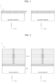
- FIGS. 1 and 2 are diagrams illustrating a process of forming a nanosheet stack of a semiconductor device according to one embodiment.
- a lower isolation layer may be formed on a semiconductor substrate sp.
- the semiconductor substrate sp may include a silicon substrate and a Si-on-insulator (SOI) substrate.
- the semiconductor substrate sp may include a p-type, n-type, or intrinsic silicon substrate.
- the lower isolation layer may be formed by forming an insulating material on the semiconductor substrate sp or through performing appropriate ground plane doping on the semiconductor substrate sp.
- the lower isolation layer of the semiconductor substrate sp may act to reduce a leakage current in an off-state of a channel formed in the semiconductor substrate sp.
- a metal gate may be formed around a Si channel layer after selective etching of a SiGe sacrificial layer in a replacement metal gate (RMG) module. Then, the metal gate of the lower isolation layer is in contact with the semiconductor substrate sp, and source/drain are formed below the lower isolation layer, and thus the lower isolation layer has a structure in the form of a planar field effect transistor (FET).
- FET planar field effect transistor
- a nanosheet stack ns_s may be formed by repeatedly and continuously growing Si epitaxial layers Si and SiGe epitaxial layers (at least one of a first sacrificial layers and a plurality of a second sacrificial layers) SiGe1 and SiGe2 on the semiconductor substrate sp.
- the Si epitaxial layer may constitute channel layers of stacked-type n-metal oxide semiconductor FET (MOSFET) and p-MOSFET devices with a complementary FET (CFET) structure.
- MOSFET n-metal oxide semiconductor FET
- CFET complementary FET
- the first sacrificial layer SiGe1 may be formed on an upper portion and a lower portion of each of at least a lower channel layer l_ch and an upper channel layer u_ch.
- the second sacrificial layer SiGe2 may be formed between the first sacrificial layers SiGe1 present between the at least lower channel layer l_ch and the upper channel layer u_ch.
- FIG. 2 An example in which two channel layers Si are formed in each of the n-MOSFET and p-MOSFET are shown in FIG. 2 .
- the present disclosure is not limited thereto.
- the number of channel layers Si may be one or three or more, and the number of Si channels may be determined through repeated growth of the SiGe epitaxial layer and the Si epitaxial layer.
- the number and type of the sacrificial layers SiGe1 and SiCe2 is not limited thereto.
- at least one type of the sacrificial layers is further included.
- the number of the first and the second sacrificial layers may be different from the FIG. 2 .
- the Si epitaxial layer Si and the SiGe epitaxial layers SiGe1 and SiGe2 may be grown by at least one low-vacuum process among remote plasma chemical vapor deposition (RPCVD), ultra-high vacuum chemical vapor deposition (UHVCVD), molecular beam epitaxy (MBE), and atomic layer deposition (ALD) growth methods. Therefore, crystallinity of the channel layer may be secured and a composition and a thickness may be precisely controlled.
- RPCVD remote plasma chemical vapor deposition
- UHVCVD ultra-high vacuum chemical vapor deposition
- MBE molecular beam epitaxy
- ALD atomic layer deposition
- the Si epitaxial layer Si (channel layer) may be formed to have a thickness of 5 nm to 30 nm.
- the SiGe epitaxial layers SiGe1 and SiGe2 (sacrificial layers) may each be formed to have a thickness of 5 nm to 30 nm.
- the SiGe epitaxial layer SiGe1 located at the top may be formed to be thicker than the other layers in consideration of thickness reduction due to subsequent processes.
- the SiGe epitaxial layer SiGe1 located at the top may be formed to have a thickness of 5 nm to 100 nm.
- the epitaxial layers may be formed so as to prevent an empty space from being formed during the formation of an inner spacer in a subsequent process.
- epitaxial growth may be performed at a Ge content of 10% to 30% of the SiGe epitaxial layer SiGe1.
- Epitaxial growth may be performed at a ratio of a Ge content of the SiGe epitaxial layer SiGe2 that is at least 20% greater than that of the SiGe epitaxial layer SiGe1.
- the first sacrificial layers SiGe1 may be a SiGe layer having a Ge content of 10% to 30%.
- the second sacrificial layer SiGe2 may be a SiGe layer having a Ge content that is at least 20% greater than that of the first sacrificial layer.
- FIGS. 3 to 7 are diagrams illustrating a process of forming a shallow trench isolation (STI) module of the semiconductor device according to one embodiment.
- STI shallow trench isolation
- an upper portion up_l including the nanosheet stack ns_s and a portion of the semiconductor substrate sp, is etched in a protruding shape using, for example, a hard mask.
- the upper portion up_l process is a process of forming a trench isolation for separation between devices and may be identical or similar to a process of forming a fin of a fin-FET.
- a silicon nitride layer (Si x N y ) liner layer ln1 is formed on the upper portion up_l by a deposition method such as LPCVD, PECVD, or ALD.
- the liner layer ln1 may be formed to have a thickness of 30 nm or less.
- the liner layer ln1 may prevent oxidation of the Si epitaxial layer and the SiGe epitaxial layers SiGe1 and SiGe2 and diffusion of Ge during a subsequent process of forming a trench isolation.
- a silicon oxide layer sl1 is grown on the entire surface of a semiconductor substrate 4 of FIG. 4 , and thus an etched region in FIG. 3 is filled with the silicon oxide layer sl1. Then, a portion of the silicon oxide layer sl1 is planarized by a chemical mechanical polishing (CMP) process.
- CMP chemical mechanical polishing
- the silicon oxide layer sl1 may be densified through a high- heat treatment process before the process of planarizing the silicon oxide layer sl1. Since the heat treatment process is performed at a temperature of 900 °C or less, Ge diffusion from the SiGe layer to the Si channel layer can be prevented.
- the silicon nitride layer liner layer ln1 may be used as an etch stop layer in the planarization process of the silicon oxide layer sl1.
- the planarization process may be performed before the silicon nitride layer liner layer ln1 is exposed.
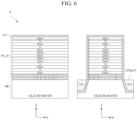
- a portion of the silicon oxide layer sl1 may be etched by an etch-back process.
- the etch-back process may be performed to a depth at which the silicon nitride layer liner layer ln1 is not etched.
- the etch-back process may be performed using a process with higher etch selectivity for the silicon oxide film sl1 than for silicon nitride layer (Si x N y ).
- an STI module STI corresponding to the remaining silicon oxide layer sl1 may be provided lower than starting heights of the Si epitaxial layer and the SiGe epitaxial layers SiGe1 and SiGe2. Accordingly, the Si epitaxial layer and the SiGe epitaxial layers SiGe1 and SiGe2 may all be exposed in subsequent processes.
- a silicon nitride layer liner layer ln2 may be grown on the STI module STI to a thickness of 30 nm or less.
- the liner layer ln1 etched together with the silicon oxide layer sl1 in FIG. 6 may also be re-grown.
- FIG. 7 an example of a case in which the process in FIG. 7 is not performed will be described.
- the present disclosure is not limited thereto.
- FIGS. 8 to 15 are diagrams illustrating a process of forming a dummy gate module of the semiconductor device according to one embodiment.
- a dummy gate Dg may be grown on the entire upper surface of the semiconductor substrate sp. Thereafter, the dummy gate Dg is planarized by a CMP process.
- the dummy gate Dg may be formed using polycrystalline Si or SiGe, or amorphous Si or SiGe.
- the dummy gate Dg may be formed using another material with high etch selectivity with respect to a silicon nitride ( protection ) layer ln1 and ln2.
- a planarization process of the dummy gate Dg may be performed so as not to expose the liner layers ln1 and ln2.
- the dummy gate Dg remaining after the planarization may be a region where a high-k insulating film and a gate metal are deposited through a subsequent process to form a gate stack.
- a dummy gate cap Dgc may be deposited on the planarized dummy gate Dg using a silicon nitride layer.
- the dummy gate cap Dgc may be used as a hard mask during etching of the channel layer Si.
- the dummy gate cap Dgc that is the silicon nitride layer is patterned through, for example, a dry etching process.
- the etching process may be performed by photolithography and a dry etching process according to, for example, a silicon channel length (or gate width of a region where the source/drain are to be formed) of the semiconductor device according to one embodiment.
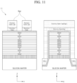
- the dummy gate cap Dgc is used as a hard mask to etch the dummy gate Dg according to the silicon channel length of the semiconductor device according to one embodiment.
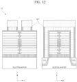
- an outer spacer os1 is formed on the side surface of the dummy gate Dg.
- the outer spacer os1 is formed as a silicon oxide layer when a thermal oxidation process is performed at a temperature of 900 °C or less.
- a thickness of the outer spacer os1 may be formed in consideration of a width of the channel layer.
- an outer spacer os2 may be formed by a process different from that of FIG. 12 .
- the outer spacer os2 may be formed by growing a specified material on the entire surface of the wafer using ALD or CVD.
- the specified material may include at least one material among a silicon oxide layer, a silicon nitride layer, or silicon carbide such as SiN, SiO, SiC, SiCO, and SiCN. Additionally, as shown in FIG.
- the outer spacer os2 may left only side surfaces of the upper portions of the dummy gate Dg and the dummy gate cap Dgc.
- the present disclosure is not limited thereto.
- wet or dry etching on the silicon nitride layer ln2 is selectively performed on the silicon nitride layer ln2 using a process with higher etch selectivity for the silicon nitride layer ln2 than for the silicon oxide layer os1.
- the silicon nitride layer In2 is etched, the upper portion of the SiGe sacrificial layer SiGe1 may be exposed.
- the dummy gate cap Dgc is also etched simultaneously with the silicon nitride layer, but the process is controlled so as not to completely remove the dummy gate cap Dgc.
- the dummy gate cap Dgc that is a silicon nitride layer and the outer spacer os1 are used as hard masks to etch the Si channel layer Si and some of the first sacrificial layer SiGe1 and the second sacrificial layers SiGe2.
- the process may be controlled to selectively etch only the Si channel layer Si, the first sacrificial layer SiGe1, and the second sacrificial layer SiGe2.
- an etch may be progressed to a depth where the nanosheet stack ep including the Si channel layer Si and the first and second sacrificial layers SiGe1 and SiGe2 are all exposed, and the trench isolation TI is exposed.
- a cavity etching process of the first and second sacrificial layers SiGe1 and SiGe2 to form an inner spacer is1 is performed as shown in FIG. 17 .
- the first and second sacrificial layers SiGe1 and SiGe2 are not completely etched, but the first and second sacrificial layers SiGe1 and SiGe2 may be selectively wet or dry etched as much as a width of the inner spacer.
- the inner spacer is1 determines a length of the Si channel and serves as a self-alignment mask during the source/drain formation, and thus uniformity is essential.
- the cavity etching process of the first and second sacrificial layers SiGe1 and SiGe2 should have a very high selectivity with respect to the dummy gate cap Dgc, the outer spacer os1, and the Si channel layer Si, and an etch rate should increase according to the Ge contents in the first and second sacrificial layers SiGe1 and SiGe2.
- an etch depth of the second sacrificial layer SiGe2 which has the Ge content that is at least 20% higher than that of the first sacrificial layer SiGe1, should be greater than that of the first sacrificial layer SiGe1 through the etching process.
- the inner spacer is1 is deposited on the entire surface, where the SiGe cavity etching process is performed, using ALD.
- the inner spacer is1 may be formed using a specified material.
- the specified material may include at least one material among a silicon oxide layer, a silicon nitride layer, or silicon carbide such as SiN, SiO, SiC, SiCO, and SiCN.
- a outside side surface of the inner spacer is1 may be gradually flat.
- FIG. 20 shows a deposition result of a specified material when only the first sacrificial layer SiGe1 is used according to another embodiment.
- a thickness of the inner spacer formed on the side surface of the first sacrificial layer SiGe1 between upper and lower Si channel layers and a thickness of the inner spacer formed on the side surface of the Si channel layer are the same or similar.
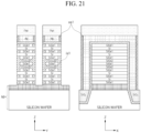
- FIG. 21 is a diagram for describing the inner spacer of the semiconductor device.
- a portion of an inner spacer material deposited on the semiconductor substrate sp is removed through an etching process.
- the inner spacer materials deposited on the side surface of the Si channel layer Si and on the top and side surfaces of the dummy gate Dg and the dummy gate cap Dgc are etched.
- the inner spacer material is deposited to be thicker on the first and second sacrificial layers SiGe1 and SiGe2 than on the Si channel layer Si.
- the etching of the inner spacer is1 may be controlled to expose only the side surface of the Si channel layer Si.
- the etching process may be performed, for example, by a wet or dry etching process or an atomic layer etch (ALE) process.
- ALE atomic layer etch
- FIG. 22 is a diagram for describing an epitaxial growth process of forming lower source/drain according to one embodiment.
- selective epitaxial growth of source/drain regions p_S0 and p_SD is performed using the Si channel layer Si, where silicon is exposed, and the lower isolation layer of the silicon substrate sp as seed layers.
- the selective epitaxial growth does not proceed on the silicon oxide layer (e.g., the inner spacer is1) but only on the exposed silicon portion.
- a lower p-MOSFET of a CFET device according to one embodiment is formed.
- a SiGe epitaxial layer doped with a p-type dopant in real-time may be selectively grown.
- doping may be performed through an ion implantation process of a p-type dopant.
- a Ge content in each of the source/drain regions p_S0 and p_SD may be 20% or more.
- FIG. 22 it can be seen that an unnecessary p-type dummy source/drain region is formed in the upper Si channel layer together with the p-type source/drain region p_SD in the lower p-MOSFET.
- the dummy source/drain p_S0 on an upper portion is removed through a subsequent process.
- FIG. 23 is a diagram illustrating a process of covering a semiconductor substrate with an insulator (organic solvent) according to one embodiment.
- an organic solvent l_de is formed to a height that is greater than that covering the dummy gate over the semiconductor substrate.
- the organic solvent l_de is an organic solvent for a semiconductor and may include, for example, propylene glycol methyl ether acetate (PGMEA), propylene glycol propyl ether (PGPE), cyclohexanone, ethyl lactate (EL), ⁇ -butyrolactone (GBL), or N-methylpyridine (NMP).
- the organic solvent may be used in photo resist (PR), bottom anti-reflective coating (BARC), or spin-on carbon (SoC).
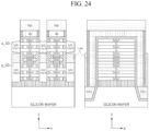
- FIG. 24 shows an etch-back process of the organic solvent l_de for a semiconductor.
- some of the organic solvent l_de for a semiconductor may be removed through an etch-back process.
- the source/drain region p_S0 formed in the upper n-MOSFET may be completely exposed, and the source/drain region p_SD formed in the lower p-MOSFET may be formed in a form covered with the organic solvent l_de for a semiconductor.
- FIG. 25 is a diagram for describing an etching process of the upper source/drain SiGe epitaxial layer.
- the dummy source/drain region p_S0 formed in the upper n-MOSFET is selectively removed by a wet or dry etching process. Since the etching process employs a process with high selectivity with respect to the Si channel layer Si, the etching process may be performed precisely so as not to affect the Si channel layer Si.
- FIG. 26 is a diagram for describing a removal process of the organic solvent l_de for a semiconductor.
- the organic solvent l_de for a semiconductor formed on the upper portion of the lower p-MOSFET may be removed.
- the organic solvent l_de for a semiconductor may be removed by an etch-back process.
- FIG. 27 is a diagram for describing an insulating process of the n-MOSFET and the P-MOSFET according to one embodiment.
- a silicon oxide layer sl2 is formed on the entire surface (e.g., in a space where the dummy source/drain region p_S0 and the organic solvent l_de are removed) of the semiconductor substrate. Thereafter, as in a second process (S27_2), a portion of the silicon oxide layer sl2 is removed through an etch-back process. As a result, the silicon oxide layer sl2 remains only on the upper portion of the p-MOSFET, and the Si channel layer Si of the upper n-MOSFET device is completely exposed.
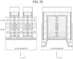
- FIG. 28 is a diagram for describing a process of forming source/drain of the upper n-MOSTFET according to one embodiment.
- a source/drain region n_SD of the n-MOSFET is formed on the upper Si channel layer Si where silicon is exposed.
- the Si epitaxial layer doped with an n-type dopant in real-time may be selectively grown.
- the source/drain region n_SD of the n-MOSFET may be formed by selectively growing the Si epitaxial layer and doping the Si epitaxial layer through an ion implantation process of an n-type dopant.
- FIGS. 29 and 30 are diagrams for describing a process of forming an inter layer dielectric (ILD).
- ILD inter layer dielectric
- an ILD that is a silicon oxide layer is formed on the entire surface (e.g., top of the upper source/drain region n_S/D and the silicon oxide layer sl2 in a thickness that covers the dummy gate cap Dgc) of the semiconductor substrate.
- the ILD formed on the semiconductor substrate sp is planarized through a CMP process to expose the dummy gate cap Dgc.
- the dummy gate cap Dgc that is the silicon nitride layer may be used as a stop layer in the planarization process. After the planarization process, the entire upper surface of the dummy gate cap Dgc may be exposed.
- FIGS. 31 , 32 , and 33 are diagrams for describing a process of exposing the first and second sacrificial layers SiGe1 and SiGe2.
- the dummy gate cap Dgc is completely removed using a wet or dry etching process with high etch selectivity with respect to a silicon oxide layer (ILD) ILD 1.
- ILD silicon oxide layer
- the dummy gate Dg is completely removed using an etching process with high etch selectivity with respect to the silicon oxide layer and the silicon nitride layer.
- the silicon nitride protection layer ln2 below the dummy gate Dg completely surrounds the Si channel layer Si. Therefore, the dummy gate Dg may be removed by wet etching.
- the silicon nitride protection layer ln2 is removed using a specified etching process to expose the Si channel layer Si, the inner spacer is1, and the first and second sacrificial layers SiGe1 and SiGe2.
- the etching process of FIG. 33 may utilize an etching process with high etching selectivity with respect to the silicon oxide layer.
- FIG. 34 is a diagram for describing a process of etching the first and second sacrificial layers SiGe1 and SiGe2.
- the first and second sacrificial layers SiGe1 and SiGe2 are selectively etched. It is important that the etching process of the first and second sacrificial layers SiGe1 and SiGe2 has very high selectivity with respect to the ILD ILD1, the outer spacer os1, the inner spacer is1, and the Si channel layer Si. Both dry etching and wet etching are possible as selective etching of the first and second sacrificial layers SiGe1 and SiGe2.
- the first and second sacrificial layers SiGe1 and SiGe2 are selectively etched on both sides of a width of the silicon channel.
- FIG. 35 is a diagram for describing a process of forming a gate dielectric insulation layer.
- a gate dielectric insulation layer sl3 is formed on all surfaces of the Si channel layer Si, both cross-sections of the inner spacer is1, and on a surface where the semiconductor substrate is exposed.
- the gate dielectric insulation layer sl3 may be formed of silicon oxide, silicon nitride, or a high-k dielectric material.
- the high-k dielectric material may include Hf, Zr, Al, La, Mg, Ba, Ti, or Pb or a metal oxide and silicate according to a combination of Hf, Zr, Al, La, Mg, Ba, Ti, and Pb.
- the gate dielectric insulation layer sl3 may be deposited with the same thickness on a three-dimensional channel using ALD.
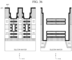
- FIG. 36 is a diagram for describing a process of forming a p-type work function metal.
- a p-type work function metal is formed on all outer surfaces of the gate dielectric insulation layer sl3. Since the p-type work function metal Wf1 should be formed to be thin with a constant thickness, the p-type work function metal Wf1 may be formed using ALD.
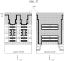
- FIG. 37 is a diagram for describing a process of forming a metal gate.
- a portion remaining after the gate dielectric insulation layer S12 and the p-type work function metal Wf1 of the semiconductor substrate are formed is filled with a metal gate L_mg.
- the metal gate L_mg may be formed in the form of at least one layer including at least one material among Ti, Al, Cu, and W.
- the metal gate L_mg may be formed by ALD in the same manner as the gate dielectric insulation layer sl3 and the p-type work function metal Wf1.
- the metal gate L_mg may be formed by electroplating or electroless plating.
- FIG. 38 is a diagram for describing an etch-back process of the metal gate.
- an etch-back process is performed on the metal gate L_mg.
- a height of the metal gate L_mg is adjusted to a height between heights of the n-MOSFET and the p-MOSFET (or, the height of the region where the p-MOSFET is formed).
- the metal gate L_mg may be etched by wet etching.
- FIG. 39 is a diagram for describing a process of etching a p-type work function metal Wf1.
- portions of the p-type work function metal Wf1 formed around the Si channel layer of the upper n-MOSFET and formed on sidewalls may be selectively etched.
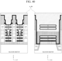
- FIGS. 40 and 41 are diagram for describing a process of forming an insulator separating the n-MOSFET from the p-MOSFET.
- an insulator s_de is formed with a high thickness on the entire surface (e.g., on top of the metal gate L_mg) of the semiconductor substrate.
- the insulator s_de is removed through an etch-back process and formed only to an upper portion of the p-MOSFET metal gate.
- FIG. 42 is a diagram for describing a process of forming an n-type work function metal.
- an n-type work function metal Wf2 is formed on all surfaces of the gate dielectric insulation layer of the Si channel layer of the upper n-MOSFET. Since the n-type work function metal Wf2 should be formed to be thin with a constant thickness, the n-type work function metal Wf2 may be formed using ALD.
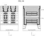
- FIGS. 43 and 44 are diagrams for describing a process of forming a gate metal.
- a portion remaining after the gate dielectric insulation layer sl3 and the n-type work function metal are formed is filled with a metal gate u_mg.
- the metal gate u_mg may be formed in the form of at least one layer including at least one material among Ti, Al, Cu, and W.
- the metal gate u_mg may be formed by at least one of ALD, electroplating, and electroless plating.
- an excess portion of the gate dielectric insulation layer sl3, the n-type work function metal Wf2 and the metal gate u_mg on the upper portion of the ILD layer may be planarized using a metal CMP process.
- a second ILD layer ILD2 is formed on the entire surface (e.g., on top of the metal gate u_mg and the gate dielectric insulation layer sl3) of the semiconductor substrate.
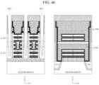
- a metal contact Mc1 is formed in the source/drain region (hereinafter, referred to as a "lower source/drain region”) (p_SD) and the metal gate region L_mg of the lower p-MOSFET.
- the metal contact Mc1 may be formed through photolithography and dry etching processes for at least a portion of each of the second ILD layer ILD2, the lower source/drain region p_SD, and the lower gate region L_mg.
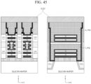
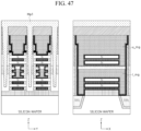
- FIGS. 47 and 48 show a process of forming a metal plug.
- a first metal plug Mp1 is formed in the upper source/drain region p_SD and the metal contact Mc1.
- a portion of the first metal plug Mp1 formed on an upper portion of the second ILD layer ILD2 may be sufficiently planarized using a metal CMP process. Then, a metal wiring process for the first metal plug Mp1 is performed.
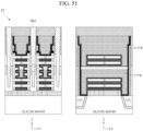
- FIGS. 48 and 51 show a process of forming a second metal plug.
- a metal etch-back process is performed by exposing only a source/drain contact Mc2 of the first metal plug Mp1.
- an insulating layer De2 is formed on the entire surface (e.g., at least portion of the source/drain contact Mc2) of the wafer.
- an etch-back process is performed on the insulating layer De2 to expose a source/drain region of the upper n-MOSFET device.
- the second metal plug Mp2 may be formed in the source/drain region of the upper n-MOSFET device. Then, a metal line process may be performed on the second metal plug Mp2.
- the source/drain regions of the n-MOSFET and the p-MOSFET may be formed through a relatively simplified process.
- the CFET semiconductor device 51 may be manufactured such that no void is generated when the inner spacer by stacking the SiGe sacrificial layers with different Ge contents, and the SiGe sacrificial layers are repeatedly stacked so that the gap between the n-MOSFET and the p-MOSFET may be formed sufficiently as desired.
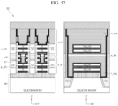
- FIG. 52 is a diagram illustrating a structure of a complementary transistor device according to one embodiment.
- a complementary transistor device 52 may include a substrate sp, a lower transistor l_tr, an upper transistor u_tr, and an inner spacer is1.
- the complementary transistor device 52 includes two transistors of the upper transistors u_tr and the lower transistor l_tr.
- the present disclosure is not limited thereto.
- the lower transistor l_tr is positioned above the substrate sp and may include a lower channel layer l_ch, a lower gate l_mg, and a lower source/drain region n_SD.
- the upper transistor u_tr is positioned above the lower transistor l_tr and may include an upper channel layer u_ch, an upper gate u_mg, and an upper source/drain region p_SD.
- the lower channel layer l_ch and the upper channel layer u_ch are repeatedly grown and are formed to include a first sacrificial layer SiGe1 and a second sacrificial layer SiGe2 between the lower channel layer l_ch and the upper channel layer u_ch. And then the lower channel layer l_ch and the upper channel layer u_ch may be formed to correspond to the transistors l_tr and u_tr through etching in an y direction (or x direction) corresponding to the channel length and removal of the first and second sacrificial layers SiGe1 and SiGe2.
- the lower source/drain region n_SD may be formed by selectively growing a Si epitaxial layer on a sidewall of the lower channel layer on the substrate and doping the Si epitaxial layer with a first dopant (e.g., a p-type dopant).
- a first dopant e.g., a p-type dopant
- the upper source/drain region p_SD may be formed by removing a dummy source/drain region formed on a sidewall of an upper channel layer together with the lower source/drain region in a state in which the lower source/drain region n_SD is covered with an organic solvent l_de and then removing the organic solvent l_de.
- the upper source/drain region p_SD may be formed by epitaxially growing the upper channel layer in a state in which a silicon oxide layer is formed only on an upper portion of the lower transistor from which the organic solvent l_de is removed.
- the inner spacer is1 may be formed by removing a portion of each of the first sacrificial layer SiGe1 and the second sacrificial layer SiGe2, which are formed above and below the lower channel layer l_ch and the upper channel layer and have different Ge contents, to a depth according to the Ge content, and then depositing an insulating material.
- the inner spacer is1 may insulate an upper gate u_mg from the lower source/drain region n_SD and insulate the upper gate u_mg from the upper source/drain region p_SD.
- the inner spacer is1 may serve as a sidewall preventing a gate length (or channel length) from decreasing to a certain value or less.
- the inner spacer is1 may be further formed between the lower transistor l_tr and the upper transistor u_tr to separate the lower transistor l_tr from the upper transistor u_tr.
- the inner spacer is1 may be positioned between the lower channel layer l_ch and the upper channel layer u_ch and configured to insulate the lower transistor l_tr from the upper transistor u_tr. Some sidewalls of the inner spacer is 1 may be formed to be thicker than sidewalls of the lower gate l_mg and the upper gate u_mg formed above and below the lower channel layer l_ch and the upper channel layer u_ch.
- the first sacrificial layer SiGe1 may be a SiGe layer having a Ge content of 10% to 30%.
- the second sacrificial layer SiGe2 may be a SiGe layer having a Ge content that is at least 20% greater than that of the first sacrificial layer.
- the inner spacer is1 may be formed by etching the second sacrificial layer SiGe2 to be deeper than the first sacrificial layer SiGe1 through cavity etching at a rate corresponding to the Ge content with high selectivity with respect to the channel layers u_ch and l_ch and depositing the insulating material on outer sides of the layers remaining after the cavity etching.
- the first sacrificial layer SiGe1 may be formed on an upper portion and a lower portion of each of at least the lower channel layer l_ch and the upper channel layer u_ch, and the second sacrificial layer SiGe2 may be formed between the first sacrificial layers SiGe1 present between the at least lower channel layer l_ch and the upper channel layer u_ch.
- the complementary transistor device 52 may further include a silicon oxide layer s12.
- the silicon oxide layer s12 may be formed between the lower source/drain region n_S/D and the upper source/drain region p_S/D to be in contact with an upper surface of the lower source/drain region n_S/D and a lower surface of the upper source/drain region p_S/D.
- the silicon oxide layer s12 may be configured to insulate the lower source/drain region n_S/D from the upper source/drain region p_S/D.
- a first work function metal WF1 is formed between the lower channel layer l_ch and the lower gate l_mg.
- a second work function metal WF2 is formed between the upper channel layer u_ch and the upper gate u_mg.
- the first and second work functions WF1, WF2 have channel characteristics the lower gate l_mg and the upper gate u_mg, respectively.
- the complementary transistor device 52 may further include an insulator s_de.
- the insulator s_de may insulate the lower gate l_mg from the upper gate u_mg between the lower gate l_mg and the upper gate u_mg.
- FIG. 53 is a flowchart illustrating a method of manufacturing a complementary transistor device according to one embodiment.
- a nanosheet stack ns_s including a lower channel layer l_ch, an upper channel layer u_ch, a plurality of first and second sacrificial layers SiGe1 and SiGe2 separating the lower channel layer l_ch from the upper channel layer u_ch may be formed through epitaxial growth.
- the first and second sacrificial layers SiGe1 and SiGe2 may have different Ge contents.
- a portion of each of the first and second sacrificial layers SiGe1 and SiGe2 may be removed through an etching process at a rate according to a Ge content. For example, a portion of each of the first and second sacrificial layers SiGe1 and SiGe2 may be removed as shown in FIG. 17 .
- an inner spacer is1 may be formed in a space where the portions of the first and second sacrificial layers SiGe1 and SiGe2 are removed.
- the inner spacer is1 may be formed in the space where the portions of the first and second sacrificial layers SiGe1 and SiGe2 are removed as shown in FIGS. 18 and 19 .
- the inner spacer is1 may be formed as a sidewall for the remaining portions of the first and second sacrificial layers SiGe1 and SiGe2 above and below the upper channel layer u_ch and the lower channel layer l_ch.
- an upper drain/source region n_SD and a lower drain/source region p_SD may be formed.
- the upper drain/source region n_SD and the lower drain/source region p_SD may be formed as shown in FIGS. 22 to 28 .
- the remaining portions of the first and second sacrificial layers SiGe1 and SiGe2 may be removed.
- the remaining portion of each of the first and second sacrificial layers SiGe1 and SiGe2 may be removed as shown in FIG. 34 .
- a metal lower gate l_mg and an upper gate u_mg may be formed in the space where the first and second sacrificial layers SiGe1 and SiGe2 are removed.
- the lower gate l_mg may be formed around the lower channel layer l_ch
- the upper gate u_mg may be formed around the upper channel layer u_ch.
- an inner spacer can be formed using sacrificial layers with different Ge contents.
- various effects can be provided that are directly or indirectly identified through the present disclosure.
- functions/operations depicted in flowchart blocks of the present specification may be performed out of the order depicted in the flowchart.
- two blocks shown in succession may in fact be executed substantially simultaneously.
- blocks may sometimes be executed in a reverse order according to involved functions/actions.
- a function of a given block of the flowchart and/or block diagram may be separated into a plurality of blocks, and/or functions of two or more blocks of the flowchart and/or block diagram may be at least partially integrated.
- other blocks may be added/inserted between the shown blocks, and/or blocks/operations may be omitted without departing from the scope of the technical spirit of the present invention.
- a component When a component is referred to as being “coupled,” “connected,” or “responsive,” or “on” other component, it may be directly coupled, connected, responsive, or on the other component, or the other component may intervene therebetween. On the other hand, when a component is “directly coupled,” “directly connected,” “directly responsive,” or “directly on” other component, no other component may intervene therebetween.
- the term “and/or” includes one or more or all combinations of the related enumerated items.
- a symbol “/” (e.g., when used in the term “source/drain”) will be understood to be identical to the term “and/or.”
- first may be used to describe various components, but the components are not limited by these terms. These terms are used only to distinguish one component from another component. For example, without departing from the scope of the present invention, a “first component” may be referred to as a "second component.”
- spatially relative terms “below,” “beneath,” “lower,” “above,” “on,” “upper,” and the like can be used to easily describe a correlation between one element or components and another element or components.
- the spatially relative terms should be understood as terms including different directions of components when the components are used or operated.
- the exemplary term “below” can include all of downward and upward directions.
- the element may also be oriented in other directions (e.g., rotated 90 degrees or in other directions), in this case, spatially relative terms may be interpreted according to the orientation.
Landscapes
- Engineering & Computer Science (AREA)
- Chemical & Material Sciences (AREA)
- Nanotechnology (AREA)
- Physics & Mathematics (AREA)
- Crystallography & Structural Chemistry (AREA)
- General Physics & Mathematics (AREA)
- Manufacturing & Machinery (AREA)
- Condensed Matter Physics & Semiconductors (AREA)
- Mathematical Physics (AREA)
- Theoretical Computer Science (AREA)
- Metal-Oxide And Bipolar Metal-Oxide Semiconductor Integrated Circuits (AREA)
- Insulated Gate Type Field-Effect Transistor (AREA)
- Thin Film Transistor (AREA)
Abstract
Description
- This application claims priority to and the benefit of
Korean Patent Applications 10-2023-0162440, filed on Nov 21, 2023 10-2024-0106019, filed on Aug 8, 2024 - Various embodiments of the present disclosure relate to a semiconductor manufacturing technology.
- As electronic devices are miniaturized and are more highly integrated, semiconductor devices mounted on the electronic devices are also becoming more integrated and ultra-fine. Since field effect transistors (FETs) are disposed horizontally on a wafer substrate in the conventional FET with a gate all around (GAA) structure, the number of applicable transistors per unit area of the wafer substrate is limited.
- In order to address the problem, a complementary-FET (CFET) with vertically stacked n-metal oxide semiconductor FET (MOSFET) and p-MOSFET of GAA structures have recently been proposed.
- However, since a CFET device is still just an idea technology, a detailed manufacturing process is not disclosed yet.
- The present disclosure is directed to providing a complementary transistor device and a control method thereof, which may form an inner spacer using sacrificial layers with different Ge contents.
- According to an aspect of the present disclosure, there is provided a transistor device including a substrate, a lower transistor positioned on the substrate and including a lower channel layer, a lower gate, and a lower source/drain region, an upper transistor positioned on the lower transistor and including an upper channel layer, an upper gate, and an upper source/drain region, and an inner spacer formed by removing a portion of each of a first sacrificial layer and a second sacrificial layer, which are formed above and below the lower channel layer and the upper channel layer and have different Ge contents, to a depth according to a Ge content and then depositing an insulating material.
- According to another aspect of the present disclosure, there is provided a method of manufacturing a transistor device, which includes forming a nanosheet stack including a lower channel layer, an upper channel layer, and a plurality of first and second sacrificial layers separating the lower channel layer from the upper channel layer, wherein the first and second sacrificial layers have different Ge contents, forming an inner spacer in a space provided by removing a portion of the first sacrificial layer and a portion of the second sacrificial layer through an etching process at a rate according to a Ge content, and forming a lower gate around the lower channel layer and an upper gate around the upper channel layer in a provided space from which the remaining portion of each of the first and second sacrificial layers is removed.
- According to still another aspect of the present disclosure, there is provided a transistor device including a nanosheet stack including a lower channel layer, an upper channel layer, and a plurality of first and second sacrificial layers separating the lower channel layer from the upper channel layer, an inner spacer formed on some side surfaces of the first and second sacrificial layers between at least the lower channel layer and the upper channel layer, a lower gate formed around the lower channel layer in a space remaining after removing the first and second sacrificial layers, and an upper gate formed around the upper channel layer, wherein the first and second sacrificial layers have different Ge contents, and the inner spacer is formed by removing a portion of the first sacrificial layer and a portion of the second sacrificial layer through an etching process at a rate according to a Ge content.
- The above and other objects, features and advantages of the present disclosure will become more apparent to those of ordinary skill in the art by describing exemplary embodiments thereof in detail with reference to the accompanying drawings, in which:
-
FIGS. 1 and 2 are diagrams illustrating a process of forming a nanosheet stack of a semiconductor device according to one embodiment; -
FIGS. 3 to 7 are diagrams illustrating a process of forming a shallow trench isolation (STI) module of the semiconductor device according to one embodiment; -
FIGS. 8 to 15 are diagrams illustrating a process of forming a dummy gate module of the semiconductor device according to one embodiment; -
FIGS. 16 to 21 are diagrams illustrating a process of forming an inner spacer module of the semiconductor device according to one embodiment; -
FIG. 22 is a diagram for describing an epitaxial growth process of forming lower source/drain according to one embodiment; -
FIGS. 23 to 28 are diagrams illustrating a process of forming and separating an n-metal oxide semiconductor field effect transistor (MOSFET) device and a p-MOSFET device; -
FIGS. 29 to 44 are diagrams for describing a process of forming a replacement metal gate (RMG); -
FIGS. 45 to 51 are diagrams for describing a process of forming a metal line; -
FIG. 52 is a diagram illustrating a structure of a complementary transistor device according to one embodiment; and -
FIG. 53 is a flowchart illustrating a method of manufacturing a complementary transistor device according to one embodiment. - In the description of the drawings, the same or similar reference numerals may be used for the same or similar components.
-
FIGS. 1 and 2 are diagrams illustrating a process of forming a nanosheet stack of a semiconductor device according to one embodiment. - Referring to
FIG. 1 , a lower isolation layer may be formed on a semiconductor substrate sp. - The semiconductor substrate sp may include a silicon substrate and a Si-on-insulator (SOI) substrate. The semiconductor substrate sp may include a p-type, n-type, or intrinsic silicon substrate.
- The lower isolation layer may be formed by forming an insulating material on the semiconductor substrate sp or through performing appropriate ground plane doping on the semiconductor substrate sp. The lower isolation layer of the semiconductor substrate sp may act to reduce a leakage current in an off-state of a channel formed in the semiconductor substrate sp.
- In the lower isolation layer, a metal gate may be formed around a Si channel layer after selective etching of a SiGe sacrificial layer in a replacement metal gate (RMG) module. Then, the metal gate of the lower isolation layer is in contact with the semiconductor substrate sp, and source/drain are formed below the lower isolation layer, and thus the lower isolation layer has a structure in the form of a planar field effect transistor (FET).
- As shown in
FIG. 2 , a nanosheet stack ns_s may be formed by repeatedly and continuously growing Si epitaxial layers Si and SiGe epitaxial layers (at least one of a first sacrificial layers and a plurality of a second sacrificial layers) SiGe1 and SiGe2 on the semiconductor substrate sp. In this regard, the Si epitaxial layer may constitute channel layers of stacked-type n-metal oxide semiconductor FET (MOSFET) and p-MOSFET devices with a complementary FET (CFET) structure. Both the first sacrificial layer SiGel and the second sacrificial layer SiGe2 may be sacrificial layers fully removed by selective etching in a subsequent process. The first sacrificial layer SiGe1 may be formed on an upper portion and a lower portion of each of at least a lower channel layer l_ch and an upper channel layer u_ch. The second sacrificial layer SiGe2 may be formed between the first sacrificial layers SiGe1 present between the at least lower channel layer l_ch and the upper channel layer u_ch. - An example in which two channel layers Si are formed in each of the n-MOSFET and p-MOSFET are shown in
FIG. 2 . However, the present disclosure is not limited thereto. For example, the number of channel layers Si may be one or three or more, and the number of Si channels may be determined through repeated growth of the SiGe epitaxial layer and the Si epitaxial layer. Similarly, the number and type of the sacrificial layers SiGe1 and SiCe2 is not limited thereto. For example, at least one type of the sacrificial layers is further included. As another example, the number of the first and the second sacrificial layers may be different from theFIG. 2 . - Since a lattice constant difference of approximately 4.3% between Si and Ge, stress may occur in the thin film during the repeated growth of the SiGe epitaxial layer and the Si epitaxial layer. When a thickness of the thin film exceeds a critical thickness in a state in which stress occurs, the stress is reduced by releasing accumulated stress energy. Then, dislocations are generated at an interface, which may degrade performance of the device and cause a leakage current.
- In order to prevent the dislocations, the Si epitaxial layer Si and the SiGe epitaxial layers SiGe1 and SiGe2 may be grown by at least one low-vacuum process among remote plasma chemical vapor deposition (RPCVD), ultra-high vacuum chemical vapor deposition (UHVCVD), molecular beam epitaxy (MBE), and atomic layer deposition (ALD) growth methods. Therefore, crystallinity of the channel layer may be secured and a composition and a thickness may be precisely controlled.
- The Si epitaxial layer Si (channel layer) may be formed to have a thickness of 5 nm to 30 nm. The SiGe epitaxial layers SiGe1 and SiGe2 (sacrificial layers) may each be formed to have a thickness of 5 nm to 30 nm. The SiGe epitaxial layer SiGe1 located at the top may be formed to be thicker than the other layers in consideration of thickness reduction due to subsequent processes. For example, the SiGe epitaxial layer SiGe1 located at the top may be formed to have a thickness of 5 nm to 100 nm.
- According to one embodiment, the epitaxial layers may be formed so as to prevent an empty space from being formed during the formation of an inner spacer in a subsequent process. For example, epitaxial growth may be performed at a Ge content of 10% to 30% of the SiGe epitaxial layer SiGe1. Epitaxial growth may be performed at a ratio of a Ge content of the SiGe epitaxial layer SiGe2 that is at least 20% greater than that of the SiGe epitaxial layer SiGe1. Specifically, the first sacrificial layers SiGe1 may be a SiGe layer having a Ge content of 10% to 30%. The second sacrificial layer SiGe2 may be a SiGe layer having a Ge content that is at least 20% greater than that of the first sacrificial layer.
-
FIGS. 3 to 7 are diagrams illustrating a process of forming a shallow trench isolation (STI) module of the semiconductor device according to one embodiment. - As shown in
FIG. 3 , an upper portion up_l, including the nanosheet stack ns_s and a portion of the semiconductor substrate sp, is etched in a protruding shape using, for example, a hard mask. The upper portion up_l process is a process of forming a trench isolation for separation between devices and may be identical or similar to a process of forming a fin of a fin-FET. - As shown in
FIG. 4 , a silicon nitride layer (SixNy) liner layer ln1 is formed on the upper portion up_l by a deposition method such as LPCVD, PECVD, or ALD. The liner layer ln1 may be formed to have a thickness of 30 nm or less. The liner layer ln1 may prevent oxidation of the Si epitaxial layer and the SiGe epitaxial layers SiGe1 and SiGe2 and diffusion of Ge during a subsequent process of forming a trench isolation. - As shown in
FIG. 5 , a silicon oxide layer sl1 is grown on the entire surface of a semiconductor substrate 4 ofFIG. 4 , and thus an etched region inFIG. 3 is filled with the silicon oxide layer sl1. Then, a portion of the silicon oxide layer sl1 is planarized by a chemical mechanical polishing (CMP) process. Here, the silicon oxide layer sl1 may be densified through a high- heat treatment process before the process of planarizing the silicon oxide layer sl1. Since the heat treatment process is performed at a temperature of 900 °C or less, Ge diffusion from the SiGe layer to the Si channel layer can be prevented. In this case, the silicon nitride layer liner layer ln1 may be used as an etch stop layer in the planarization process of the silicon oxide layer sl1. Alternatively, the planarization process may be performed before the silicon nitride layer liner layer ln1 is exposed. - As shown in
FIG. 6 , a portion of the silicon oxide layer sl1 may be etched by an etch-back process. In this case, the etch-back process may be performed to a depth at which the silicon nitride layer liner layer ln1 is not etched. In this regard, the etch-back process may be performed using a process with higher etch selectivity for the silicon oxide film sl1 than for silicon nitride layer (SixNy). In this case, an STI module STI corresponding to the remaining silicon oxide layer sl1 may be provided lower than starting heights of the Si epitaxial layer and the SiGe epitaxial layers SiGe1 and SiGe2. Accordingly, the Si epitaxial layer and the SiGe epitaxial layers SiGe1 and SiGe2 may all be exposed in subsequent processes. - As shown in
FIG. 7 , a silicon nitride layer liner layer ln2 may be grown on the STI module STI to a thickness of 30 nm or less. In this case, the liner layer ln1 etched together with the silicon oxide layer sl1 inFIG. 6 may also be re-grown. Hereinafter, an example of a case in which the process inFIG. 7 is not performed will be described. However, the present disclosure is not limited thereto. -
FIGS. 8 to 15 are diagrams illustrating a process of forming a dummy gate module of the semiconductor device according to one embodiment. - As shown in
FIG. 8 , a dummy gate Dg may be grown on the entire upper surface of the semiconductor substrate sp. Thereafter, the dummy gate Dg is planarized by a CMP process. The dummy gate Dg may be formed using polycrystalline Si or SiGe, or amorphous Si or SiGe. Alternatively, the dummy gate Dg may be formed using another material with high etch selectivity with respect to a silicon nitride ( protection ) layer ln1 and ln2. Here, a planarization process of the dummy gate Dg may be performed so as not to expose the liner layers ln1 and ln2. The dummy gate Dg remaining after the planarization may be a region where a high-k insulating film and a gate metal are deposited through a subsequent process to form a gate stack. - As shown in
FIG. 9 , a dummy gate cap Dgc may be deposited on the planarized dummy gate Dg using a silicon nitride layer. The dummy gate cap Dgc may be used as a hard mask during etching of the channel layer Si. - Referring to
FIG. 10 , the dummy gate cap Dgc that is the silicon nitride layer is patterned through, for example, a dry etching process. The etching process may be performed by photolithography and a dry etching process according to, for example, a silicon channel length (or gate width of a region where the source/drain are to be formed) of the semiconductor device according to one embodiment. - Referring to
FIG. 11 , the dummy gate cap Dgc is used as a hard mask to etch the dummy gate Dg according to the silicon channel length of the semiconductor device according to one embodiment. - Hereinafter, a process of forming an outer spacer on a side surface of the dummy gate Dg will be described with reference to
FIGS. 12 to 15 . - As shown in
FIG. 12 , an outer spacer os1 is formed on the side surface of the dummy gate Dg. The outer spacer os1 is formed as a silicon oxide layer when a thermal oxidation process is performed at a temperature of 900 °C or less. During the thermal oxidation process, since the silicon oxide layer is grown simultaneously from an initial boundary surface in a direction away from a horizontal center of the semiconductor substrate sp, a thickness of the outer spacer os1 may be formed in consideration of a width of the channel layer. - Alternatively, as shown in
FIGS. 13 and14 , an outer spacer os2 may be formed by a process different from that ofFIG. 12 . As shown inFIG. 13 , the outer spacer os2 may be formed by growing a specified material on the entire surface of the wafer using ALD or CVD. The specified material may include at least one material among a silicon oxide layer, a silicon nitride layer, or silicon carbide such as SiN, SiO, SiC, SiCO, and SiCN. Additionally, as shown inFIG. 14 , since the upper portion of the grown outer spacer layer os2 is etched by an anisotropic etching process, the outer spacer os2 may left only side surfaces of the upper portions of the dummy gate Dg and the dummy gate cap Dgc. Hereinafter, an example in which the outer spacer os1 ofFIG. 12 is applied will be described. However, the present disclosure is not limited thereto. - As shown in
FIG. 15 , wet or dry etching on the silicon nitride layer ln2 is selectively performed on the silicon nitride layer ln2 using a process with higher etch selectivity for the silicon nitride layer ln2 than for the silicon oxide layer os1. As the silicon nitride layer In2 is etched, the upper portion of the SiGe sacrificial layer SiGe1 may be exposed. In this case, the dummy gate cap Dgc is also etched simultaneously with the silicon nitride layer, but the process is controlled so as not to completely remove the dummy gate cap Dgc. - Hereinafter, a process of forming an inner spacer module of the semiconductor device according to one embodiment will be described with reference to
FIGS. 16 to 21 . - As shown in
FIG. 16 , the dummy gate cap Dgc that is a silicon nitride layer and the outer spacer os1 are used as hard masks to etch the Si channel layer Si and some of the first sacrificial layer SiGe1 and the second sacrificial layers SiGe2. InFIG. 16 , by using a process with high etch selectivity with respect to the silicon oxide layer and the silicon nitride layer, the process may be controlled to selectively etch only the Si channel layer Si, the first sacrificial layer SiGe1, and the second sacrificial layer SiGe2. InFIG. 16 , an etch may be progressed to a depth where the nanosheet stack ep including the Si channel layer Si and the first and second sacrificial layers SiGe1 and SiGe2 are all exposed, and the trench isolation TI is exposed. - In a structure in which the Si channel layer Si and the first and second sacrificial layers SiGe1 and SiGe2 are exposed as shown in
FIG. 16 , a cavity etching process of the first and second sacrificial layers SiGe1 and SiGe2 to form an inner spacer is1 is performed as shown inFIG. 17 . - In the cavity etching process, the first and second sacrificial layers SiGe1 and SiGe2 are not completely etched, but the first and second sacrificial layers SiGe1 and SiGe2 may be selectively wet or dry etched as much as a width of the inner spacer. The inner spacer is1 determines a length of the Si channel and serves as a self-alignment mask during the source/drain formation, and thus uniformity is essential.
- The cavity etching process of the first and second sacrificial layers SiGe1 and SiGe2 should have a very high selectivity with respect to the dummy gate cap Dgc, the outer spacer os1, and the Si channel layer Si, and an etch rate should increase according to the Ge contents in the first and second sacrificial layers SiGe1 and SiGe2.
- In this way, an etch depth of the second sacrificial layer SiGe2, which has the Ge content that is at least 20% higher than that of the first sacrificial layer SiGe1, should be greater than that of the first sacrificial layer SiGe1 through the etching process.
- As shown in
FIG. 18 , the inner spacer is1 is deposited on the entire surface, where the SiGe cavity etching process is performed, using ALD. The inner spacer is1 may be formed using a specified material. The specified material may include at least one material among a silicon oxide layer, a silicon nitride layer, or silicon carbide such as SiN, SiO, SiC, SiCO, and SiCN. - As shown in
FIG. 19 , when the specified material is formed on the remaining side surfaces of each of the first and second sacrificial layers SiGe1 and SiGe2 ofFIG. 16 using ALD, a outside side surface of the inner spacer is1 may be gradually flat. -
FIG. 20 shows a deposition result of a specified material when only the first sacrificial layer SiGe1 is used according to another embodiment. - Referring to
FIG. 20 , unlike one embodiment, when only the SiGe sacrificial layer SiGe1 with the same Ge content is used, it can be seen that no insulating material is deposited on some side surface of the first sacrificial layer SiGe1. In this case, a gap between the n-MOSFET and the p-MOSFET, which are to be vertically stacked in a subsequent process is not electrically insulated, a CFET structure cannot be formed. Specifically, in the left case ofFIG. 20 , a thickness of the inner spacer formed on the side surface of the first sacrificial layer SiGe1 between upper and lower Si channel layers and a thickness of the inner spacer formed on the side surface of the Si channel layer are the same or similar. Thus, since the etching is performed at the same thickness during the etching of the formed inner spacers, empty space may be generated in the inner spacers. Consequently, a problem in that the source/drain are formed in an unnecessary portion during a subsequent source/drain epitaxial growth may occur. -
FIG. 21 is a diagram for describing the inner spacer of the semiconductor device. - Referring to
FIG. 21 , a portion of an inner spacer material deposited on the semiconductor substrate sp is removed through an etching process. In the etching process, the inner spacer materials deposited on the side surface of the Si channel layer Si and on the top and side surfaces of the dummy gate Dg and the dummy gate cap Dgc are etched. The inner spacer material is deposited to be thicker on the first and second sacrificial layers SiGe1 and SiGe2 than on the Si channel layer Si. In the etching process, the etching of the inner spacer is1 may be controlled to expose only the side surface of the Si channel layer Si. The etching process may be performed, for example, by a wet or dry etching process or an atomic layer etch (ALE) process. The inner spacer material remaining through the above-described etching process may form the inner spacer is1 as shown inFIG. 21 . - Hereinafter, a process of forming sources/drains of the n-MOSFET and the p-MOSFET will be described with reference to
FIG. 22 . -
FIG. 22 is a diagram for describing an epitaxial growth process of forming lower source/drain according to one embodiment. - Referring to
FIG. 22 , selective epitaxial growth of source/drain regions p_S0 and p_SD is performed using the Si channel layer Si, where silicon is exposed, and the lower isolation layer of the silicon substrate sp as seed layers. The selective epitaxial growth does not proceed on the silicon oxide layer (e.g., the inner spacer is1) but only on the exposed silicon portion. A lower p-MOSFET of a CFET device according to one embodiment is formed. To this end, a SiGe epitaxial layer doped with a p-type dopant in real-time may be selectively grown. Alternatively, after the SiGe epitaxial layer is selectively grown, doping may be performed through an ion implantation process of a p-type dopant. In this case, a Ge content in each of the source/drain regions p_S0 and p_SD may be 20% or more. - In
FIG. 22 , it can be seen that an unnecessary p-type dummy source/drain region is formed in the upper Si channel layer together with the p-type source/drain region p_SD in the lower p-MOSFET. However, due to the structure of the designed CFET device, the dummy source/drain p_S0 on an upper portion is removed through a subsequent process. - Hereinafter, a process of forming and separating the n-MOSFET device and the p-MOSFET device will be described with reference to
FIGS. 23 to 28 . -
FIG. 23 is a diagram illustrating a process of covering a semiconductor substrate with an insulator (organic solvent) according to one embodiment. - Referring to
FIG. 23 , an organic solvent l_de is formed to a height that is greater than that covering the dummy gate over the semiconductor substrate. The organic solvent l_de is an organic solvent for a semiconductor and may include, for example, propylene glycol methyl ether acetate (PGMEA), propylene glycol propyl ether (PGPE), cyclohexanone, ethyl lactate (EL), γ-butyrolactone (GBL), or N-methylpyridine (NMP). The organic solvent may be used in photo resist (PR), bottom anti-reflective coating (BARC), or spin-on carbon (SoC). -
FIG. 24 shows an etch-back process of the organic solvent l_de for a semiconductor. - As shown in
FIG. 24 , some of the organic solvent l_de for a semiconductor may be removed through an etch-back process. As a result, the source/drain region p_S0 formed in the upper n-MOSFET may be completely exposed, and the source/drain region p_SD formed in the lower p-MOSFET may be formed in a form covered with the organic solvent l_de for a semiconductor. -
FIG. 25 is a diagram for describing an etching process of the upper source/drain SiGe epitaxial layer. - As shown in
FIG. 25 , the dummy source/drain region p_S0 formed in the upper n-MOSFET is selectively removed by a wet or dry etching process. Since the etching process employs a process with high selectivity with respect to the Si channel layer Si, the etching process may be performed precisely so as not to affect the Si channel layer Si. -
FIG. 26 is a diagram for describing a removal process of the organic solvent l_de for a semiconductor. - As shown in
FIG. 26 , the organic solvent l_de for a semiconductor formed on the upper portion of the lower p-MOSFET may be removed. For example, the organic solvent l_de for a semiconductor may be removed by an etch-back process. -
FIG. 27 is a diagram for describing an insulating process of the n-MOSFET and the P-MOSFET according to one embodiment. - Referring to
FIG. 27 , as in a first process (S27_1), a silicon oxide layer sl2 is formed on the entire surface (e.g., in a space where the dummy source/drain region p_S0 and the organic solvent l_de are removed) of the semiconductor substrate. Thereafter, as in a second process (S27_2), a portion of the silicon oxide layer sl2 is removed through an etch-back process. As a result, the silicon oxide layer sl2 remains only on the upper portion of the p-MOSFET, and the Si channel layer Si of the upper n-MOSFET device is completely exposed. -
FIG. 28 is a diagram for describing a process of forming source/drain of the upper n-MOSTFET according to one embodiment. - As shown in
FIG. 28 , a source/drain region n_SD of the n-MOSFET is formed on the upper Si channel layer Si where silicon is exposed. For example, the Si epitaxial layer doped with an n-type dopant in real-time may be selectively grown. As another example, the source/drain region n_SD of the n-MOSFET may be formed by selectively growing the Si epitaxial layer and doping the Si epitaxial layer through an ion implantation process of an n-type dopant. - Hereinafter, a process of forming the RMG will be described with reference to
FIGS. 29 to 44 . This may be a process in which the dummy gate Dg is converted into an actual metal gate region. -
FIGS. 29 and30 are diagrams for describing a process of forming an inter layer dielectric (ILD). - As shown in
FIG. 29 , an ILD that is a silicon oxide layer is formed on the entire surface (e.g., top of the upper source/drain region n_S/D and the silicon oxide layer sl2 in a thickness that covers the dummy gate cap Dgc) of the semiconductor substrate. - As shown in
FIG. 30 , the ILD formed on the semiconductor substrate sp is planarized through a CMP process to expose the dummy gate cap Dgc. In this case, the dummy gate cap Dgc that is the silicon nitride layer may be used as a stop layer in the planarization process. After the planarization process, the entire upper surface of the dummy gate cap Dgc may be exposed. -
FIGS. 31 ,32 , and33 are diagrams for describing a process of exposing the first and second sacrificial layers SiGe1 and SiGe2. - As shown in
FIG. 31 , the dummy gate cap Dgc is completely removed using a wet or dry etching process with high etch selectivity with respect to a silicon oxide layer (ILD)ILD 1. - As shown in
FIG. 32 , the dummy gate Dg is completely removed using an etching process with high etch selectivity with respect to the silicon oxide layer and the silicon nitride layer. The silicon nitride protection layer ln2 below the dummy gate Dg completely surrounds the Si channel layer Si. Therefore, the dummy gate Dg may be removed by wet etching. - As shown in
FIG. 33 , the silicon nitride protection layer ln2 is removed using a specified etching process to expose the Si channel layer Si, the inner spacer is1, and the first and second sacrificial layers SiGe1 and SiGe2. The etching process ofFIG. 33 may utilize an etching process with high etching selectivity with respect to the silicon oxide layer. -
FIG. 34 is a diagram for describing a process of etching the first and second sacrificial layers SiGe1 and SiGe2. - As shown in
FIG. 34 , in a state in which the side surfaces of the first and second sacrificial layers SiGe1 and SiGe2 and the Si channel layer Si are exposed, the first and second sacrificial layers SiGe1 and SiGe2 are selectively etched. It is important that the etching process of the first and second sacrificial layers SiGe1 and SiGe2 has very high selectivity with respect to the ILD ILD1, the outer spacer os1, the inner spacer is1, and the Si channel layer Si. Both dry etching and wet etching are possible as selective etching of the first and second sacrificial layers SiGe1 and SiGe2. The first and second sacrificial layers SiGe1 and SiGe2 are selectively etched on both sides of a width of the silicon channel. -
FIG. 35 is a diagram for describing a process of forming a gate dielectric insulation layer. - As shown in
FIG. 35 , a gate dielectric insulation layer sl3 is formed on all surfaces of the Si channel layer Si, both cross-sections of the inner spacer is1, and on a surface where the semiconductor substrate is exposed. The gate dielectric insulation layer sl3 may be formed of silicon oxide, silicon nitride, or a high-k dielectric material. The high-k dielectric material may include Hf, Zr, Al, La, Mg, Ba, Ti, or Pb or a metal oxide and silicate according to a combination of Hf, Zr, Al, La, Mg, Ba, Ti, and Pb. The gate dielectric insulation layer sl3 may be deposited with the same thickness on a three-dimensional channel using ALD. -
FIG. 36 is a diagram for describing a process of forming a p-type work function metal. - As shown in
FIG. 36 , a p-type work function metal is formed on all outer surfaces of the gate dielectric insulation layer sl3. Since the p-type work function metal Wf1 should be formed to be thin with a constant thickness, the p-type work function metal Wf1 may be formed using ALD. -
FIG. 37 is a diagram for describing a process of forming a metal gate. - As shown in
FIG. 37 , a portion remaining after the gate dielectric insulation layer S12 and the p-type work function metal Wf1 of the semiconductor substrate are formed is filled with a metal gate L_mg. - The metal gate L_mg may be formed in the form of at least one layer including at least one material among Ti, Al, Cu, and W. The metal gate L_mg may be formed by ALD in the same manner as the gate dielectric insulation layer sl3 and the p-type work function metal Wf1. Alternatively, the metal gate L_mg may be formed by electroplating or electroless plating.
-
FIG. 38 is a diagram for describing an etch-back process of the metal gate. - As shown in
FIG. 38 , an etch-back process is performed on the metal gate L_mg. A height of the metal gate L_mg is adjusted to a height between heights of the n-MOSFET and the p-MOSFET (or, the height of the region where the p-MOSFET is formed). For the etching process of a three-dimensional complicated structure, the metal gate L_mg may be etched by wet etching. -
FIG. 39 is a diagram for describing a process of etching a p-type work function metal Wf1. - As shown in
FIG. 39 , portions of the p-type work function metal Wf1 formed around the Si channel layer of the upper n-MOSFET and formed on sidewalls may be selectively etched. -
FIGS. 40 and41 are diagram for describing a process of forming an insulator separating the n-MOSFET from the p-MOSFET. - As shown in
FIG. 40 , an insulator s_de is formed with a high thickness on the entire surface (e.g., on top of the metal gate L_mg) of the semiconductor substrate. - As shown in
FIG. 41 , the insulator s_de is removed through an etch-back process and formed only to an upper portion of the p-MOSFET metal gate. -
FIG. 42 is a diagram for describing a process of forming an n-type work function metal. - As shown in
FIG. 42 , an n-type work function metal Wf2 is formed on all surfaces of the gate dielectric insulation layer of the Si channel layer of the upper n-MOSFET. Since the n-type work function metal Wf2 should be formed to be thin with a constant thickness, the n-type work function metal Wf2 may be formed using ALD. -
FIGS. 43 and44 are diagrams for describing a process of forming a gate metal. - As shown in
FIG. 43 , a portion remaining after the gate dielectric insulation layer sl3 and the n-type work function metal are formed is filled with a metal gate u_mg. The metal gate u_mg may be formed in the form of at least one layer including at least one material among Ti, Al, Cu, and W. The metal gate u_mg may be formed by at least one of ALD, electroplating, and electroless plating. - As shown in
FIG. 44 , an excess portion of the gate dielectric insulation layer sl3, the n-type work function metal Wf2 and the metal gate u_mg on the upper portion of the ILD layer may be planarized using a metal CMP process. - Hereinafter, a process of forming a metal line will be described with reference to
FIGS. 45 to 51 . - As shown in
FIG. 45 , a second ILD layer ILD2 is formed on the entire surface (e.g., on top of the metal gate u_mg and the gate dielectric insulation layer sl3) of the semiconductor substrate. - As shown in
FIG. 46 , a metal contact Mc1 is formed in the source/drain region (hereinafter, referred to as a "lower source/drain region") (p_SD) and the metal gate region L_mg of the lower p-MOSFET. The metal contact Mc1 may be formed through photolithography and dry etching processes for at least a portion of each of the second ILD layer ILD2, the lower source/drain region p_SD, and the lower gate region L_mg. -
FIGS. 47 and48 show a process of forming a metal plug. - As shown in
FIG. 47 , a first metal plug Mp1 is formed in the upper source/drain region p_SD and the metal contact Mc1. - As shown in
FIG. 48 , a portion of the first metal plug Mp1 formed on an upper portion of the second ILD layer ILD2 may be sufficiently planarized using a metal CMP process. Then, a metal wiring process for the first metal plug Mp1 is performed. -
FIGS. 48 and51 show a process of forming a second metal plug. - As shown in
FIG. 48 , a metal etch-back process is performed by exposing only a source/drain contact Mc2 of the first metal plug Mp1. - As shown in
FIG. 49 , an insulating layer De2 is formed on the entire surface (e.g., at least portion of the source/drain contact Mc2) of the wafer. - As shown in
FIG. 50 , an etch-back process is performed on the insulating layer De2 to expose a source/drain region of the upper n-MOSFET device. - As shown in
FIG. 51 , the second metal plug Mp2 may be formed in the source/drain region of the upper n-MOSFET device. Then, a metal line process may be performed on the second metal plug Mp2. - In this way, in a
CFET semiconductor device 51 according to one embodiment, the source/drain regions of the n-MOSFET and the p-MOSFET may be formed through a relatively simplified process. - In addition, the
CFET semiconductor device 51 according to one embodiment may be manufactured such that no void is generated when the inner spacer by stacking the SiGe sacrificial layers with different Ge contents, and the SiGe sacrificial layers are repeatedly stacked so that the gap between the n-MOSFET and the p-MOSFET may be formed sufficiently as desired. -
FIG. 52 is a diagram illustrating a structure of a complementary transistor device according to one embodiment. - Referring to
FIG. 52 , acomplementary transistor device 52 according to one embodiment may include a substrate sp, a lower transistor l_tr, an upper transistor u_tr, and an inner spacer is1. InFIG. 52 , an example in which thecomplementary transistor device 52 includes two transistors of the upper transistors u_tr and the lower transistor l_tr will be described. However, the present disclosure is not limited thereto. - The lower transistor l_tr is positioned above the substrate sp and may include a lower channel layer l_ch, a lower gate l_mg, and a lower source/drain region n_SD.
- The upper transistor u_tr is positioned above the lower transistor l_tr and may include an upper channel layer u_ch, an upper gate u_mg, and an upper source/drain region p_SD.
- The lower channel layer l_ch and the upper channel layer u_ch are repeatedly grown and are formed to include a first sacrificial layer SiGe1 and a second sacrificial layer SiGe2 between the lower channel layer l_ch and the upper channel layer u_ch. And then the lower channel layer l_ch and the upper channel layer u_ch may be formed to correspond to the transistors l_tr and u_tr through etching in an y direction (or x direction) corresponding to the channel length and removal of the first and second sacrificial layers SiGe1 and SiGe2.
- The lower source/drain region n_SD may be formed by selectively growing a Si epitaxial layer on a sidewall of the lower channel layer on the substrate and doping the Si epitaxial layer with a first dopant (e.g., a p-type dopant).
- The upper source/drain region p_SD may be formed by removing a dummy source/drain region formed on a sidewall of an upper channel layer together with the lower source/drain region in a state in which the lower source/drain region n_SD is covered with an organic solvent l_de and then removing the organic solvent l_de. The upper source/drain region p_SD may be formed by epitaxially growing the upper channel layer in a state in which a silicon oxide layer is formed only on an upper portion of the lower transistor from which the organic solvent l_de is removed.
- The inner spacer is1 may be formed by removing a portion of each of the first sacrificial layer SiGe1 and the second sacrificial layer SiGe2, which are formed above and below the lower channel layer l_ch and the upper channel layer and have different Ge contents, to a depth according to the Ge content, and then depositing an insulating material. The inner spacer is1 may insulate an upper gate u_mg from the lower source/drain region n_SD and insulate the upper gate u_mg from the upper source/drain region p_SD. As a result, the inner spacer is1 may serve as a sidewall preventing a gate length (or channel length) from decreasing to a certain value or less. The inner spacer is1 may be further formed between the lower transistor l_tr and the upper transistor u_tr to separate the lower transistor l_tr from the upper transistor u_tr.
- The inner spacer is1 may be positioned between the lower channel layer l_ch and the upper channel layer u_ch and configured to insulate the lower transistor l_tr from the upper transistor u_tr. Some sidewalls of the inner spacer is 1 may be formed to be thicker than sidewalls of the lower gate l_mg and the upper gate u_mg formed above and below the lower channel layer l_ch and the upper channel layer u_ch.
- The first sacrificial layer SiGe1 may be a SiGe layer having a Ge content of 10% to 30%. The second sacrificial layer SiGe2 may be a SiGe layer having a Ge content that is at least 20% greater than that of the first sacrificial layer.
- The inner spacer is1 may be formed by etching the second sacrificial layer SiGe2 to be deeper than the first sacrificial layer SiGe1 through cavity etching at a rate corresponding to the Ge content with high selectivity with respect to the channel layers u_ch and l_ch and depositing the insulating material on outer sides of the layers remaining after the cavity etching.
- The first sacrificial layer SiGe1 may be formed on an upper portion and a lower portion of each of at least the lower channel layer l_ch and the upper channel layer u_ch, and the second sacrificial layer SiGe2 may be formed between the first sacrificial layers SiGe1 present between the at least lower channel layer l_ch and the upper channel layer u_ch.
- The
complementary transistor device 52 may further include a silicon oxide layer s12. The silicon oxide layer s12 may be formed between the lower source/drain region n_S/D and the upper source/drain region p_S/D to be in contact with an upper surface of the lower source/drain region n_S/D and a lower surface of the upper source/drain region p_S/D. The silicon oxide layer s12 may be configured to insulate the lower source/drain region n_S/D from the upper source/drain region p_S/D. - A first work function metal WF1 is formed between the lower channel layer l_ch and the lower gate l_mg. A second work function metal WF2 is formed between the upper channel layer u_ch and the upper gate u_mg. The first and second work functions WF1, WF2 have channel characteristics the lower gate l_mg and the upper gate u_mg, respectively.
- The
complementary transistor device 52 may further include an insulator s_de. The insulator s_de may insulate the lower gate l_mg from the upper gate u_mg between the lower gate l_mg and the upper gate u_mg. -
FIG. 53 is a flowchart illustrating a method of manufacturing a complementary transistor device according to one embodiment. - Referring to
FIG. 53 , inoperation 5310, a nanosheet stack ns_s including a lower channel layer l_ch, an upper channel layer u_ch, a plurality of first and second sacrificial layers SiGe1 and SiGe2 separating the lower channel layer l_ch from the upper channel layer u_ch may be formed through epitaxial growth. The first and second sacrificial layers SiGe1 and SiGe2 may have different Ge contents. - In
operation 5320, a portion of each of the first and second sacrificial layers SiGe1 and SiGe2 may be removed through an etching process at a rate according to a Ge content. For example, a portion of each of the first and second sacrificial layers SiGe1 and SiGe2 may be removed as shown inFIG. 17 . - In
operation 5330, an inner spacer is1 may be formed in a space where the portions of the first and second sacrificial layers SiGe1 and SiGe2 are removed. For example, the inner spacer is1 may be formed in the space where the portions of the first and second sacrificial layers SiGe1 and SiGe2 are removed as shown inFIGS. 18 and 19 . Inoperation 5330, the inner spacer is1 may be formed as a sidewall for the remaining portions of the first and second sacrificial layers SiGe1 and SiGe2 above and below the upper channel layer u_ch and the lower channel layer l_ch. - In
operation 5340, an upper drain/source region n_SD and a lower drain/source region p_SD may be formed. For example, the upper drain/source region n_SD and the lower drain/source region p_SD may be formed as shown inFIGS. 22 to 28 . - In
operation 5350, the remaining portions of the first and second sacrificial layers SiGe1 and SiGe2 may be removed. For example, the remaining portion of each of the first and second sacrificial layers SiGe1 and SiGe2 may be removed as shown inFIG. 34 . - In
operation 5360, a metal lower gate l_mg and an upper gate u_mg may be formed in the space where the first and second sacrificial layers SiGe1 and SiGe2 are removed. The lower gate l_mg may be formed around the lower channel layer l_ch, and the upper gate u_mg may be formed around the upper channel layer u_ch. - According to various embodiments disclosed in the present disclosure, an inner spacer can be formed using sacrificial layers with different Ge contents. In addition, various effects can be provided that are directly or indirectly identified through the present disclosure.
- It should be understood that the various embodiments and terms used in this specification are not intended to limit the technical features described herein to specific embodiments, but rather to encompass various modifications, equivalents, or alternatives of the embodiments. In the description of the drawings, similar reference numerals may be used for similar or related components. The singular form of a noun corresponding to an item may include one or more of the items, unless the context clearly indicates otherwise. In the present specification, phrases such as "A or B," "at least one of A and B," "at least one of A or B," "A, B or C," "at least one of A, B and C," and "at least one of A, B, or C" may each include any one of the items listed together in the corresponding phrase among the above phrases or all possible combinations thereof. The terms "first," "second," "primary," and "secondary" may be merely used to distinguish a corresponding component from another corresponding component and may not limit corresponding components in another aspect (e.g., importance or an order).
- The embodiments described herein will be described with reference to cross-sectional views, which are ideal schematic diagrams of the present invention. Therefore, the shape of an exemplary diagram may be modified by manufacturing techniques and/or tolerances. Accordingly, the embodiments of the present invention are not limited to specific shapes shown in the drawings, and include alternations in shape that is produced according to the manufacturing process.
- It should be noted that in some alternative embodiments, functions/operations depicted in flowchart blocks of the present specification may be performed out of the order depicted in the flowchart. For example, two blocks shown in succession may in fact be executed substantially simultaneously. Alternatively, blocks may sometimes be executed in a reverse order according to involved functions/actions. In addition, a function of a given block of the flowchart and/or block diagram may be separated into a plurality of blocks, and/or functions of two or more blocks of the flowchart and/or block diagram may be at least partially integrated. In addition, other blocks may be added/inserted between the shown blocks, and/or blocks/operations may be omitted without departing from the scope of the technical spirit of the present invention.
- Unless defined otherwise, all terms (including technical and scientific terms) used herein may be used in a sense commonly understood by those skilled in the art to which the present invention pertains. Terms defined in commonly used dictionaries are to be understood as not being ideally or excessively interpreted unless explicitly and specifically defined otherwise.
- Terms used herein are for the purpose of describing the embodiments and are not intended to limit the present specification. In the present specification, the singular form includes the plural form unless specifically stated otherwise in the context. In the present application, the terms "comprising," "having," or the like are used to specify that a feature, a number, a step, an operation, a component, an element, or a combination thereof described herein exists, and they do not preclude the presence or addition of one or more other features, numbers, steps, operations, components, elements, or combinations thereof.
- When a component is referred to as being "coupled," "connected," or "responsive," or "on" other component, it may be directly coupled, connected, responsive, or on the other component, or the other component may intervene therebetween. On the other hand, when a component is "directly coupled," "directly connected," "directly responsive," or "directly on" other component, no other component may intervene therebetween. In the present specification, the term "and/or" includes one or more or all combinations of the related enumerated items. In addition, a symbol "/" (e.g., when used in the term "source/drain") will be understood to be identical to the term "and/or."
- The terms "first," "second," and the like may be used to describe various components, but the components are not limited by these terms. These terms are used only to distinguish one component from another component. For example, without departing from the scope of the present invention, a "first component" may be referred to as a "second component."
- As shown in the drawings, spatially relative terms "below," "beneath," "lower," "above," "on," "upper," and the like can be used to easily describe a correlation between one element or components and another element or components. In addition to a direction shown in the drawings, the spatially relative terms should be understood as terms including different directions of components when the components are used or operated. For example, when an element shown in the drawing is inverted, the element described as being "below or beneath" another element may be disposed "above" another element. Consequently, the exemplary term "below" can include all of downward and upward directions. The element may also be oriented in other directions (e.g., rotated 90 degrees or in other directions), in this case, spatially relative terms may be interpreted according to the orientation.
- In the present specification, many different embodiments are disclosed in conjunction with the drawings and the above-described description. It should be understood that it may be excessively repetitive and confusing to fully describe and illustrate all combinations and sub-combinations of these embodiments. Therefore, it should be construed that the detailed description including the drawings is intended to be a complete description of all the combinations and sub-combinations of the embodiments described herein and of the methods and processes for manufacturing and using them, and is intended to support claims relating to such combinations or sub-combinations.
- The inventions disclosed above are considered as embodiments and therefore should not be construed as limiting, and the appended claims should be understood to include modifications, additions, and other embodiments according to the spirit of the present invention. Accordingly, the scope of protection of the present invention should be determined to the maximum extent permitted by the law by the fullest interpretation of the following claims and their equivalents, and should not be limited by the detailed description.
Claims (15)
- A transistor device comprising:a substrate;a lower transistor positioned on the substrate and including a lower channel layer, a lower gate, and a lower source/drain region;an upper transistor positioned on the lower transistor and including an upper channel layer, an upper gate, and an upper source/drain region; andan inner spacer positioned between the lower channel layer and the upper channel layer, and configured to insulate the lower transistor from the upper transistor,wherein some sidewalls of the inner spacer are formed to be thicker than sidewalls of the lower gate and the upper gate formed above and below the lower channel layer and the upper channel layer.
- The transistor device of claim 1, wherein the inner spacer is formed by removing a portion of each of a first sacrificial layer and a second sacrificial layer, which are formed above and below the lower channel layer and the upper channel layer and have different Ge contents each other, to a depth according to a Ge content and then depositing an insulating material.
- The transistor device of claim 2, wherein the inner spacer is formed by etching the second sacrificial layer to be deeper than the first sacrificial layer through cavity etching at a rate corresponding to the Ge content with high selectivity with respect to the channel layers and depositing the insulating material on outer sides of the layers remaining after the cavity etching.
- The transistor device of claim 2 or 3, wherein:the first sacrificial layer is formed upper and lower portions of each of at least the lower channel layer and the upper channel layer; andthe second sacrificial layer is formed between the first sacrificial layers between the at least lower channel layer and the upper channel layer.
- The transistor device of one of claims 2 to 4, wherein:the inner spacer is formed to be in contact with at least some side surfaces of each of the first sacrificial layer and the second sacrificial layer between the lower channel layer and the upper channel layer; andthe lower gate and the upper gate are formed around the lower channel layer and the upper channel layer of a space remaining by removing the first sacrificial layer and the second sacrificial layer.
- The transistor device of one of claims 1 to 5, further comprising a silicon oxide layer (s12) formed between the lower source/drain region and the upper source/drain region to be in contact with an upper surface of the lower source/drain region and a lower surface of the upper source/drain region and configured to insulate the lower source/drain region from the upper source/drain region.
- The transistor device of one of claims 1 to 6, wherein:a first work function metal is formed between the lower channel layer and the lower gate;a second work function metal is formed between the upper channel layer and the upper gate; andthe first and second work functions have channel characteristics the lower gate and the upper gate, respectively.
- The transistor device of claim 7, further comprising an insulator (s_de) configured to insulate the lower gate from the upper gate between the lower gate and the upper gate.
- A method of manufacturing a transistor device, comprising:forming a nanosheet stack including a lower channel layer, an upper channel layer, and at least one of a first sacrificial layers and a plurality of second sacrificial layers separating the lower channel layer from the upper channel layer, wherein the first and second sacrificial layers have different Ge contents;forming an inner spacer in a space provided by removing a portion of the first sacrificial layers and a portion of the second sacrificial layers through an etching process at a rate according to a Ge content; andforming a lower gate around the lower channel layer and an upper gate around the upper channel layer in a provided space from which a remaining portion of each of the first and second sacrificial layers is removed.
- The method of claim 9, wherein the forming of the inner spacer includes:forming the nanosheet stack such that the first sacrificial layers are included between the lower channel layer and the upper channel layer and the plurality of second sacrificial layers are included between the first sacrificial layers;etching a portion of each of the first and second sacrificial layers at an etching rate according to the Ge content, wherein a sidewall of the plurality of second sacrificial layers are etched to be deeper than sidewalls of the first sacrificial layers; andforming the inner spacer by depositing an insulating material on the sidewalls of each of the first and second sacrificial layers.
- The method of claim 9 or 10, further comprising, after the forming of the inner spacer and before the forming of the gates, forming a lower source/drain region on a sidewall of the lower channel layer using a substrate below the lower channel layer.
- The method of claim 11, further comprising:covering the lower source/drain region with an organic solvent, removing a dummy source/drain region in a state in which the dummy source/drain region formed on a sidewall of the upper channel layer is exposed together with the lower source/drain region, and then removing the organic solvent;forming a silicon oxide layer on an outer surface of the nanosheet stack from which the organic solvent is removed; andforming an upper source/drain region on the sidewall of the upper channel layer on the silicon oxide layer.
- The method of one of claims 9 to 12, further comprising:forming a dummy gate on an outer side of the nanosheet stack; andforming an outer spacer by depositing a silicon oxide layer on a side surface of the dummy gate through a thermal oxidation process,wherein the outer spacer forms sidewalls of the dummy gate and the space from which the remaining portion of the first and second sacrificial layers is removed.
- The method of claim 13, further comprising:forming a dummy gate cap on the dummy gate; andetching the dummy gate, the upper channel layer, and the lower channel layer according to a specified channel length using the dummy gate cap as a hard mask.
- A transistor device comprising:a substrate;a lower transistor positioned on the substrate and including a lower channel layer, a lower gate, and a lower source/drain region; andan upper transistor positioned on the lower transistor and including an upper channel layer, an upper gate, and an upper source/drain region,wherein an upper end portion of the lower gate and, an insulator (s_de), and a lower end portion of the upper gate, andwhen viewed from one side of the transistor device, a width of at least one among the upper end portion of the lower gate and, the insulator (s_de), and the lower end portion of the upper gate is formed to be thinner than the remaining widths of the lower gate and the upper gate, which are formed below the lower channel layer and above the upper channel layer, respectively.
Applications Claiming Priority (2)
| Application Number | Priority Date | Filing Date | Title |
|---|---|---|---|
| KR20230162440 | 2023-11-21 | ||
| KR1020240106019A KR102966590B1 (en) | 2023-11-21 | 2024-08-08 | Complementary fet device and the control method |
Publications (2)
| Publication Number | Publication Date |
|---|---|
| EP4561296A2 true EP4561296A2 (en) | 2025-05-28 |
| EP4561296A3 EP4561296A3 (en) | 2025-10-08 |
Family
ID=93456062
Family Applications (1)
| Application Number | Title | Priority Date | Filing Date |
|---|---|---|---|
| EP24211343.9A Pending EP4561296A3 (en) | 2023-11-21 | 2024-11-07 | Complementary fet device and control method thereof |
Country Status (5)
| Country | Link |
|---|---|
| US (1) | US20250169139A1 (en) |
| EP (1) | EP4561296A3 (en) |
| JP (1) | JP2025084098A (en) |
| CN (1) | CN120035217A (en) |
| TW (1) | TW202537457A (en) |
Cited By (1)
| Publication number | Priority date | Publication date | Assignee | Title |
|---|---|---|---|---|
| EP4718982A1 (en) * | 2024-09-26 | 2026-04-01 | INTEL Corporation | Gate-all-around integrated circuit structures having differentiated release layers |
Families Citing this family (2)
| Publication number | Priority date | Publication date | Assignee | Title |
|---|---|---|---|---|
| US20250169186A1 (en) * | 2023-11-22 | 2025-05-22 | Samsung Electronics Co., Ltd. | Transistor device having semiconductor spacer, and fabrication method thereof |
| CN120640766B (en) * | 2025-05-28 | 2026-01-23 | 北京集成电路装备创新中心有限公司 | Method for manufacturing vertical stacked semiconductor device and semiconductor device |
Family Cites Families (8)
| Publication number | Priority date | Publication date | Assignee | Title |
|---|---|---|---|---|
| US10418449B2 (en) * | 2018-01-10 | 2019-09-17 | Globalfoundries Inc. | Circuits based on complementary field-effect transistors |
| US11374003B2 (en) * | 2019-04-12 | 2022-06-28 | Taiwan Semiconductor Manufacturing Co., Ltd. | Integrated circuit |
| US11164792B2 (en) * | 2020-01-08 | 2021-11-02 | International Business Machines Corporation | Complementary field-effect transistors |
| US11282838B2 (en) * | 2020-07-09 | 2022-03-22 | International Business Machines Corporation | Stacked gate structures |
| US12641850B2 (en) * | 2021-11-03 | 2026-05-26 | Intel Corporation | Lattice stack for internal spacer fabrication |
| US12336294B2 (en) * | 2021-11-10 | 2025-06-17 | International Business Machines Corporation | Gate-cut and separation techniques for enabling independent gate control of stacked transistors |
| US20230178436A1 (en) * | 2021-12-08 | 2023-06-08 | Tokyo Electron Limited | 3d nano sheet with high density 3d metal routing |
| US11955384B2 (en) * | 2022-02-17 | 2024-04-09 | Taiwan Semiconductor Manufacturing Company, Ltd. | Stacked semiconductor device with nanostructure channels and manufacturing method thereof |
-
2024
- 2024-11-07 EP EP24211343.9A patent/EP4561296A3/en active Pending
- 2024-11-13 US US18/945,658 patent/US20250169139A1/en active Pending
- 2024-11-18 JP JP2024201143A patent/JP2025084098A/en active Pending
- 2024-11-21 TW TW113144783A patent/TW202537457A/en unknown
- 2024-11-21 CN CN202411671645.8A patent/CN120035217A/en active Pending
Cited By (1)
| Publication number | Priority date | Publication date | Assignee | Title |
|---|---|---|---|---|
| EP4718982A1 (en) * | 2024-09-26 | 2026-04-01 | INTEL Corporation | Gate-all-around integrated circuit structures having differentiated release layers |
Also Published As
| Publication number | Publication date |
|---|---|
| CN120035217A (en) | 2025-05-23 |
| EP4561296A3 (en) | 2025-10-08 |
| US20250169139A1 (en) | 2025-05-22 |
| JP2025084098A (en) | 2025-06-02 |
| TW202537457A (en) | 2025-09-16 |
Similar Documents
| Publication | Publication Date | Title |
|---|---|---|
| US11563120B2 (en) | FinFET structures and methods of forming the same | |
| US10541331B2 (en) | Fabrication of a vertical fin field effect transistor with an asymmetric gate structure | |
| US20220359206A1 (en) | Cut metal gate refill with void | |
| US11973077B2 (en) | Semiconductor device and manufacturing method thereof | |
| US11637101B2 (en) | Semiconductor device and manufacturing method thereof | |
| US11056401B2 (en) | Semiconductor device and method for manufacturing the same | |
| CN108431953B (en) | Vertical transistor fabrication and device | |
| US9741716B1 (en) | Forming vertical and horizontal field effect transistors on the same substrate | |
| US9728466B1 (en) | Vertical field effect transistors with metallic source/drain regions | |
| US20250169139A1 (en) | Complementary fet device and control method thereof | |
| WO2021081155A1 (en) | Methods for gaa i/o formation by selective epi regrowth | |
| US9543323B2 (en) | Strain release in PFET regions | |
| JP2008506271A (en) | Formation of active region using semiconductor growth process without STI integration | |
| US11610980B2 (en) | Method for processing a FinFET device | |
| KR20210123207A (en) | Semiconductor device and method | |
| KR20200113181A (en) | Liner structure in interlayer dielectric structure for semiconductor devices | |
| US12051700B2 (en) | Semiconductor device and method | |
| WO2014071653A1 (en) | Semiconductor device and manufacturing method therefor | |
| US20240355820A1 (en) | Integrated circuit structure and manufacturing method thereof | |
| US9559018B2 (en) | Dual channel finFET with relaxed pFET region | |
| US20240387285A1 (en) | Method for manufacturing semiconductor device | |
| KR102966590B1 (en) | Complementary fet device and the control method |
Legal Events
| Date | Code | Title | Description |
|---|---|---|---|
| PUAI | Public reference made under article 153(3) epc to a published international application that has entered the european phase |
Free format text: ORIGINAL CODE: 0009012 |
|
| STAA | Information on the status of an ep patent application or granted ep patent |
Free format text: STATUS: THE APPLICATION HAS BEEN PUBLISHED |
|
| AK | Designated contracting states |
Kind code of ref document: A2 Designated state(s): AL AT BE BG CH CY CZ DE DK EE ES FI FR GB GR HR HU IE IS IT LI LT LU LV MC ME MK MT NL NO PL PT RO RS SE SI SK SM TR |
|
| RIC1 | Information provided on ipc code assigned before grant |
Ipc: H10D 88/00 20250101ALI20250526BHEP Ipc: H10D 84/85 20250101ALI20250526BHEP Ipc: H10D 84/01 20250101ALI20250526BHEP Ipc: H10D 30/00 20250101ALI20250526BHEP Ipc: H10D 30/01 20250101ALI20250526BHEP Ipc: H10D 62/10 20250101AFI20250526BHEP |
|
| PUAL | Search report despatched |
Free format text: ORIGINAL CODE: 0009013 |
|
| AK | Designated contracting states |
Kind code of ref document: A3 Designated state(s): AL AT BE BG CH CY CZ DE DK EE ES FI FR GB GR HR HU IE IS IT LI LT LU LV MC ME MK MT NL NO PL PT RO RS SE SI SK SM TR |
|
| RIC1 | Information provided on ipc code assigned before grant |
Ipc: H10D 62/10 20250101AFI20250904BHEP Ipc: H10D 30/01 20250101ALI20250904BHEP Ipc: H10D 30/00 20250101ALI20250904BHEP Ipc: H10D 84/01 20250101ALI20250904BHEP Ipc: H10D 84/85 20250101ALI20250904BHEP Ipc: H10D 88/00 20250101ALI20250904BHEP |
|
| STAA | Information on the status of an ep patent application or granted ep patent |
Free format text: STATUS: REQUEST FOR EXAMINATION WAS MADE |
|
| 17P | Request for examination filed |
Effective date: 20260325 |