EP4561001A1 - Digital polar transmitter, method for improving a digital polar transmitter, and corresponding computer program - Google Patents
Digital polar transmitter, method for improving a digital polar transmitter, and corresponding computer program Download PDFInfo
- Publication number
- EP4561001A1 EP4561001A1 EP23211896.8A EP23211896A EP4561001A1 EP 4561001 A1 EP4561001 A1 EP 4561001A1 EP 23211896 A EP23211896 A EP 23211896A EP 4561001 A1 EP4561001 A1 EP 4561001A1
- Authority
- EP
- European Patent Office
- Prior art keywords
- signal
- polar transmitter
- phase
- digital polar
- modulating unit
- Prior art date
- Legal status (The legal status is an assumption and is not a legal conclusion. Google has not performed a legal analysis and makes no representation as to the accuracy of the status listed.)
- Pending
Links
Images



Classifications
-
- H—ELECTRICITY
- H04—ELECTRIC COMMUNICATION TECHNIQUE
- H04L—TRANSMISSION OF DIGITAL INFORMATION, e.g. TELEGRAPHIC COMMUNICATION
- H04L27/00—Modulated-carrier systems
- H04L27/32—Carrier systems characterised by combinations of two or more of the types covered by groups H04L27/02, H04L27/10, H04L27/18 or H04L27/26
- H04L27/34—Amplitude- and phase-modulated carrier systems, e.g. quadrature-amplitude modulated carrier systems
- H04L27/36—Modulator circuits; Transmitter circuits
- H04L27/361—Modulation using a single or unspecified number of carriers, e.g. with separate stages of phase and amplitude modulation
-
- H—ELECTRICITY
- H04—ELECTRIC COMMUNICATION TECHNIQUE
- H04B—TRANSMISSION
- H04B1/00—Details of transmission systems, not covered by a single one of groups H04B3/00 - H04B13/00; Details of transmission systems not characterised by the medium used for transmission
- H04B1/02—Transmitters
- H04B1/04—Circuits
-
- H—ELECTRICITY
- H03—ELECTRONIC CIRCUITRY
- H03C—MODULATION
- H03C5/00—Amplitude modulation and angle modulation produced simultaneously or at will by the same modulating signal
-
- H—ELECTRICITY
- H03—ELECTRONIC CIRCUITRY
- H03F—AMPLIFIERS
- H03F3/00—Amplifiers with only discharge tubes or only semiconductor devices as amplifying elements
- H03F3/189—High-frequency amplifiers, e.g. radio frequency amplifiers
- H03F3/19—High-frequency amplifiers, e.g. radio frequency amplifiers with semiconductor devices only
-
- H—ELECTRICITY
- H03—ELECTRONIC CIRCUITRY
- H03F—AMPLIFIERS
- H03F3/00—Amplifiers with only discharge tubes or only semiconductor devices as amplifying elements
- H03F3/20—Power amplifiers, e.g. Class B amplifiers, Class C amplifiers
- H03F3/24—Power amplifiers, e.g. Class B amplifiers, Class C amplifiers of transmitter output stages
- H03F3/245—Power amplifiers, e.g. Class B amplifiers, Class C amplifiers of transmitter output stages with semiconductor devices only
-
- H—ELECTRICITY
- H03—ELECTRONIC CIRCUITRY
- H03G—CONTROL OF AMPLIFICATION
- H03G3/00—Gain control in amplifiers or frequency changers
- H03G3/20—Automatic control
- H03G3/30—Automatic control in amplifiers having semiconductor devices
- H03G3/3036—Automatic control in amplifiers having semiconductor devices in high-frequency amplifiers or in frequency-changers
- H03G3/3042—Automatic control in amplifiers having semiconductor devices in high-frequency amplifiers or in frequency-changers in modulators, frequency-changers, transmitters or power amplifiers
-
- H—ELECTRICITY
- H04—ELECTRIC COMMUNICATION TECHNIQUE
- H04L—TRANSMISSION OF DIGITAL INFORMATION, e.g. TELEGRAPHIC COMMUNICATION
- H04L27/00—Modulated-carrier systems
- H04L27/32—Carrier systems characterised by combinations of two or more of the types covered by groups H04L27/02, H04L27/10, H04L27/18 or H04L27/26
- H04L27/34—Amplitude- and phase-modulated carrier systems, e.g. quadrature-amplitude modulated carrier systems
-
- H—ELECTRICITY
- H03—ELECTRONIC CIRCUITRY
- H03F—AMPLIFIERS
- H03F2200/00—Indexing scheme relating to amplifiers
- H03F2200/451—Indexing scheme relating to amplifiers the amplifier being a radio frequency amplifier
Definitions
- the invention relates to a digital polar transmitter with improved transmission behavior, a method for improving the transmission behavior of a digital polar transmitter, and a computer program with program code means to make at least a part or all of the steps of such a method.
- US 2002/0121892 A1 relates to a method and an apparatus to characterize a modulator without requiring access to modulator local oscillators.
- a periodic signal is input so that at least two tones are output, and the envelope of the filtered output is detected.
- the modulated output signal is generally differentially filtered before envelope detection.
- the measured amplitude and phase of the envelope of the differentially filtered modulator output frequencies, combined with the known filter characteristics, are used to deduce the amplitude and phase of the modulated output.
- the modulator input signal frequencies may be controlled to substantially limit the output to frequencies which differ from a reference frequency by odd multiples of a delta frequency, reducing intermodulation components.
- the modulator output may be deduced from a squared envelope signal without a need for differential filtering.
- the deduced output compared to the known input, characterizes the modulator at the input frequencies. Disadvantageously, such a characterization does not allow for synchronization of the corresponding amplitude and phase path of a digital polar transmitter in a particularly accurate and efficient manner.
- a digital polar transmitter with improved transmission behavior a method for improving the transmission behavior of a digital polar transmitter, and a computer program with program code means to make at least a part or all of the steps of such a method, wherein a particularly high accuracy of the synchronization of the corresponding amplitude and phase path of the digital polar transmitter and/or a particularly efficient corresponding operation are/is ensured.
- a digital polar transmitter with improved transmission behavior comprises a first modulating unit, especially a first modulating unit, with a first variable gain being controllable with the aid of a first phase-referred signal, a second modulating unit, especially a second modulating unit, with a second variable gain being controllable with the aid of second phase-referred signal, a third modulating unit, especially an amplitude modulating unit, with a third variable gain being controllable with the aid of an amplitude-referred signal, and an adding unit for forming the sum of an output of the first modulating unit and an output of the second modulating unit and providing said sum at an adding unit output.
- the first phase-referred signal and the second phase-referred signal are synchronized.
- the amplitude-referred signal is synchronized with respect to the first phase-referred signal and/or the second phase-referred signal.
- a particularly high accuracy of the synchronization of the corresponding amplitude and phase path of the digital polar transmitter and/or a particularly efficient corresponding operation, especially due to a corresponding single-shot calibration, are/is ensured.
- the digital polar transmitter further comprises a driver unit for providing a driver unit output on the basis of the adding unit output.
- the third modulating unit is configured to amplify the driver unit output and to provide the correspondingly amplified driver unit output at a third modulating unit output.
- accuracy and/or efficiency can further be increased.
- At least the first modulating unit and the second modulating unit are configured to form a phase shifting and/or modulating unit, preferably a cartesian-based phase shifting and/or modulating unit, comprising a corresponding phase path.
- at least the third modulating unit is configured to form a digital-to-analog converter, preferably a radio frequency digital-to-analog converter, comprising a corresponding amplitude path.
- the phase path and the amplitude path can be synchronized in a particularly accurate and efficient manner. Further advantageously, especially with the aid of the cartesian-based phase shifting and/or modulating unit, full range excitation can efficiently be achieved.
- first modulating unit and the second modulating unit are configured to form a phase modulator during corresponding normal operation.
- at least the first modulating unit and the second modulating unit are configured to form a cartesian modulator during corresponding calibration.
- a delay between the phase path and the amplitude path is compensated preferably on the basis of a delay estimation.
- inaccuracies can efficiently be reduced.
- the delay estimation is based on a first signal sequence and/or a second signal sequence extracted from an output signal of the digital polar transmitter preferably for the case that a multisine signal is applied to the digital polar transmitter.
- a multisine signal is applied to the digital polar transmitter.
- the first signal sequence comprises or is a first part of the output signal of the digital polar transmitter, wherein in said first part, only the corresponding amplitude is modulating.
- the second signal sequence comprises or is a second part of the output signal of the digital polar transmitter, wherein in said second part only the corresponding phase is modulating.
- these are the slices in time where the corresponding spectrum looks clean.
- the basis of the delay estimation is refined or substituted by a quotient signal obtained by dividing, preferably point-wise dividing, a first spectrum of the first signal sequence through a second spectrum of the second signal sequence.
- a quotient signal obtained by dividing, preferably point-wise dividing, a first spectrum of the first signal sequence through a second spectrum of the second signal sequence.
- the corresponding frequency bins of the one signal path are point-wise or bin-wise divided by the other.
- the basis of the delay estimation is refined or substituted by the slope of the corresponding phase of the quotient signal.
- the slope of the corresponding phase corresponds to the time delay of the two paths.
- a frequency response of the driver unit is equalized.
- equalization can compensate for different frequency shaping on the phase samples compared to the amplitude samples.
- the first modulating unit comprises or is a first variable-gain amplifier.
- the second modulating unit comprises or is a second variable-gain amplifier.
- the third modulating unit comprises or is a third variable-gain amplifier.
- a method for improving the transmission behavior of a digital polar transmitter comprises the steps of applying a multisine signal to the digital polar transmitter, extracting a first signal sequence and/or a second signal sequence from an output signal of the digital polar transmitter for a delay estimation, and compensating a delay between the corresponding phase path of a phase shifting and/or modulating unit, preferably a cartesian-based phase shifting and/or modulating unit, and the corresponding amplitude path of a digital-to-analog converter, preferably a radio frequency digital-to-analog converter, on the basis of said delay estimation.
- a particularly high accuracy of the synchronization of the corresponding amplitude and phase path of the digital polar transmitter and/or a particularly efficient corresponding operation, especially due to a corresponding single-shot calibration, are/is ensured. Further advantageously, a corresponding optimum minimum point can reliably and/or always be found.
- the first signal sequence comprises or is a first part of the output signal of the digital polar transmitter, wherein in said first part, only the corresponding amplitude is modulating.
- the second signal sequence comprises or is a second part of the output signal of the digital polar transmitter, wherein in said second part only the corresponding phase is modulating.
- these are the slices in time where the corresponding spectrum looks clean.
- the basis of the delay estimation is refined or substituted by a quotient signal obtained by dividing, preferably point-wise or bin-wise dividing, a first spectrum of the first signal sequence through a second spectrum of the second signal sequence.
- a quotient signal obtained by dividing, preferably point-wise or bin-wise dividing, a first spectrum of the first signal sequence through a second spectrum of the second signal sequence.
- the corresponding frequency bins of the one signal path are point-wise or bin-wise divided by the other.
- an exemplary embodiment of a digital polar transmitter 10 with improved transmission behavior comprises a first modulating unit 11a, especially a first phase modulating unit, with a first variable gain being controllable with the aid of a first phase-referred signal ⁇ ( t ), a second modulating unit 11b, especially a second phase modulating unit, with a second variable gain being controllable with the aid of second phase-referred signal ⁇ ( t ), an adding unit 12 for forming the sum of an output of the first modulating unit 11a, exemplarily denoted as signal ⁇ ( t ), and an output of the second modulating unit 11b, exemplarily denoted as signal b ( t ), and providing said sum at an adding unit output, exemplarily denoted as signal x ( t ), and a driver unit 13 for providing a driver unit output, exemplarily denoted as signal w ( t ), on the basis of the adding unit output.
- the corresponding output of the adding unit 12 is exemplarily connected to the corresponding input of the driver unit 13.
- the first phase-referred signal ⁇ ( t ) and the second phase-referred signal ⁇ ( t ) are synchronized. It is noted that it is particularly advantageous if the corresponding phase path is synched with the corresponding amplitude path.
- an input of the first modulating unit 11a is directly supplied by a signal generated by signal generating unit 15, whereas an input of the second modulating unit 11b is supplied by said signal generated by said signal generating unit 15 via a 90 degrees phase shifter 16 or a hybrid.
- the digital polar transmitter 10 comprises a third modulating unit 14, especially an amplitude modulating unit, with a third variable gain being controllable with the aid of an amplitude-referred signal ⁇ ( t ).
- the third modulating unit 14 is configured to amplify the driver unit output, exemplarily the signal w ( t ), and to provide the correspondingly amplified driver unit output at a third modulating unit output, exemplarily denoted as signal y ( t ).
- the amplitude-referred signal ⁇ ( t ) is synchronized with respect to the first phase-referred signal ⁇ ( t ) and/or the second phase-referred signal ⁇ ( t ). It is noted that it might be particularly advantageous if the first phase-referred signal ⁇ ( t ), the second phase-referred signal ⁇ ( t ), and the amplitude-referred signal ⁇ ( t ) are synchronized.
- At least the first modulating unit 11a and the second modulating unit 11b are exemplarily configured to form a phase shifting and/or modulating unit, especially a cartesian-based phase shifting and/or modulating unit, comprising a corresponding phase path, especially the above-mentioned corresponding phase path.
- At least the third modulating unit 14 is exemplarily configured to form a digital-to-analog converter, preferably a radio frequency digital-to-analog converter, comprising a corresponding amplitude path, especially the above-mentioned corresponding amplitude path.
- the phase shifting and/or modulating unit exemplarily comprises a cartesian topology, comprising a hybrid with the first modulating unit 11a, exemplarily being a first variable-gain amplifier, and the second modulating unit 11b, exemplarily being a second variable-gain amplifier.
- the radio frequency digital-to-analog converter is given by the third modulating unit 14, exemplarily being a third variable-gain amplifier.
- corresponding non-idealities that are calibrated is the delay between the phase samples ⁇ ( t ) and ⁇ ( t ) on the one hand, and ⁇ ( t ) on the other hand.
- the corresponding frequency response of the driver unit 13, exemplarily denoted as G x ⁇ w ( f ) can be equalized.
- said frequency response can exemplarily be estimated by taking the ratio of the respective Fourier transforms, especially FFTs, of the above-mentioned signals w ( t ) and x ( t ) .
- a delay between the above-mentioned phase path and the above-mentioned amplitude path is exemplarily compensated on the basis of a delay estimation.
- the delay estimation is exemplarily based on a first signal sequence and/or a second signal sequence extracted from an output signal of the digital polar transmitter 10 for the case that a multisine signal is applied to the digital polar transmitter 10.
- said multisine signal is used to measure the delay between said phase and amplitude path.
- the delay between amplitude and phase can be found in a single measurement without iteration.
- such a multisine signal especially is a signal that is the sum of a sinusoid with a fixed period and all its harmonics.
- the amplitude A k of the frequency components is taken equal while the phase is often or preferably randomized. It is noted that it might be particularly advantageous if the multisine signal comprises the least Peak-to-Average-power ratio (PAPR). Advantageously, this makes the spectral purity of the measured data higher.
- PAPR Peak-to-Average-power ratio
- a multisine signal preferably with a small PAPR is generated especially in the context of said delay estimation.
- Said multisine signal is applied to the digital polar transmitter 10 such that a corresponding version for the amplitude path and the phase path is created. It might be particularly advantageous if the two correspondingly deduced signals are as big as possible such that the effect of quantization noise is reduced.
- the correspondingly full code range can be covered.
- these two signals are exemplarily both repeated at least twice in order to get a full period where no overlap of the two paths occur.
- a constant sequence can be added as long as the other signal modulates, behind the other a constant sequence can be added as long as the first modulates. This way, in the case without delay between the two paths, one signal path 'talks' or modulates, respectively, while the other is silent (constant programming code) or at constant maximum code, respectively, and vice versa.
- this sequence is sent to the amplitude path and to the phase path and the output of the digital polar transmitter 10 is measured.
- the digital polar transmitter 10 may especially comprises a control unit configured to perform and/or support at least a part of the above-mentioned signal generation, preferably multisine signal generation, and/or at least a part of the signal measurement as described above and below.
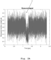
- FIG. 2A An exemplary time domain representation of the correspondingly measured signal can be seen in Fig. 2A , whereas the corresponding spectrogram of this measured signal is illustrated by Fig. 2B .
- a region 21 exemplarily a middle region
- the corresponding signal looks different as both above-mentioned two signals modulate at the same time in that region 21.
- a sequence where only the amplitude is modulating and a sequence where only the phase is modulating are extracted from the corresponding measurement.
- the above-mentioned first signal sequence especially comprises or is a first part of the output signal of the digital polar transmitter 10, wherein in said first part, only the corresponding amplitude is modulating.
- the above-mentioned second signal sequence especially comprises or is a second part of the output signal of the digital polar transmitter 10, wherein in said second part only the corresponding phase is modulating.
- these are the slices in time where the corresponding spectrum looks clean.
- the basis of the delay estimation can be refined or substituted by a quotient signal obtained by dividing, preferably point-wise dividing, a first spectrum of the first signal sequence through a second spectrum of the second signal sequence.
- the basis of the delay estimation can be refined or substituted by the slope of the corresponding phase of the above-mentioned quotient signal.
- the slope of the phase especially gives back the delay between the two signal paths. The bigger the slope, the more delay there is between the two paths.
- the transfer function of H ( ⁇ ) can preferably be the corresponding equalization filter to compensate for the different frequency shaping on the phase samples compared to the amplitude samples. Multiplying the phase samples in the frequency domain with the inverse of H ( ⁇ ) not only compensates for the delay but also equalizes these samples especially such that higher bandwidths are advantageously achieved.
- the first modulating unit 11a is part of an I-path in the phase shifting and/or modulating unit or the cartesian-based phase shifting and/or modulating unit, respectively
- the second modulating unit 11b is part of a Q-path in the phase shifting and/or modulating unit or the cartesian-based phase shifting and/or modulating unit, respectively.
- said driver unit 13 exemplarily comprises a first filter 13a, especially a first bandpass filter, an amplifier 13b, and a second filter or a matching network 13c, especially a second bandpass filter or a matching network with bandpass filter characteristic.
- the above-mentioned signal x(t) is filtered with the aid of the first filter 13a, then amplified with the aid of the amplifier 13b, and afterwards filtered with the aid of the second filter or processed in the sense of matching of impedances with the aid of the matching network 13c to form the above-mentioned signal w ( t ).
- the matching of impedances comprises or is matching of impedances of cascading power amplifier stages.
- the above-mentioned signal y ( t ) is exemplarily filtered with the aid of a third filter or output matching network 17, especially a third bandpass filter or a matching network configured to match the corresponding impedances, to form a signal m ( t ) .
- the corresponding frequency response of the third filter 17 is exemplarily denoted as G Y ⁇ M ( f ) .
- control unit of the digital polar transmitter 10 or an external device exemplarily a transmission behavior improving device, can be configured to apply a training sequence to the digital polar transmitter.
- the Q-path in the phase shifting and/or modulating unit is modulated by two periods of the same multisine signal, while the amplitude path is at maximum code, and the I-path is fully off. It is noted that it might be particularly advantageous if the above-mentioned control unit of the digital polar transmitter 10 or the above-mentioned external device, exemplarily the above-mentioned transmission behavior improving device, respectively, is configured accordingly especially to achieve this.
- the Q-path is at maximum code, while the amplitude path is modulated with two periods of the multisine signal. It is noted that it might be particularly advantageous if the above-mentioned control unit of the digital polar transmitter 10 or the above-mentioned external device, exemplarily the above-mentioned transmission behavior improving device, respectively, is configured accordingly especially to achieve this.
- the correspondingly performed measurement comprises a part where both paths modulate and a part where none modulates.
- one slice is taken where only the amplitude path modulates, and one slice is taken where only the phase shifting and/or modulating unit modulates.
- the corresponding delay and equalization filter can be calculated preferably for the corresponding phase shifting and/or modulating unit samples. It is noted that it might be particularly advantageous if the above-mentioned control unit of the digital polar transmitter 10 or the above-mentioned external device, exemplarily the above-mentioned transmission behavior improving device, respectively, is configured accordingly especially to achieve this.
- phase samples can be synchronized and equalized with the amplitude samples.
- a further advantage is that one multisine-based training sequence allows to characterize both the amplitude and phase signal path while one can only measure at one output.
- Fig. 4 shows a flow chart of an exemplary embodiment of the method for improving the transmission behavior of a digital polar transmitter such as the digital polar transmitter 10 according to Fig. 1 .
- a first step 101 comprises applying a multisine signal to the digital polar transmitter.
- a second step 102 comprises extracting a first signal sequence and/or a second signal sequence from an output signal of the digital polar transmitter for a delay estimation.
- a third step 103 comprises compensating a delay between the corresponding phase path of a phase shifting and/or modulating unit, preferably a cartesian-based phase shifting and/or modulating unit, and the corresponding amplitude path of a digital-to-analog converter, preferably a radio frequency digital-to-analog converter, on the basis of said delay estimation.
- the first signal sequence comprises or is a first part of the output signal of the digital polar transmitter, wherein in said first part, only the corresponding amplitude is modulating.
- the second signal sequence may comprise or be a second part of the output signal of the digital polar transmitter, wherein in said second part only the corresponding phase is modulating.
- the basis of the delay estimation is refined or substituted by a quotient signal obtained by dividing, preferably point-wise dividing, a first spectrum of the first signal sequence through a second spectrum of the second signal sequence.
Landscapes
- Engineering & Computer Science (AREA)
- Computer Networks & Wireless Communication (AREA)
- Signal Processing (AREA)
- Power Engineering (AREA)
- Transmitters (AREA)
Abstract
A digital polar transmitter (10) with improved transmission behavior is provided. Said digital polar transmitter (10) comprises a first modulating unit (11a) with a first variable gain being controllable with the aid of a first phase-referred signal ( α(t)), a second modulating unit (11b) with a second variable gain being controllable with the aid of second phase-referred signal ( β(t)), a third modulating unit (14), especially an amplitude modulating unit, with a third variable gain being controllable with the aid of an amplitude-referred signal ( γ(t)), and an adding unit (12) for forming the sum of an output of the first modulating unit (11a) and an output of the second modulating unit (11b) and providing said sum at an adding unit output. In this context, the first phase-referred signal ( α(t)) and the second phase-referred signal ( β(t)) are synchronized. In addition to this, the amplitude-referred signal (γ(t)) is synchronized with respect to the first phase-referred signal ( α(t)) and/or the second phase-referred signal ( β(t)).
Description
- The invention relates to a digital polar transmitter with improved transmission behavior, a method for improving the transmission behavior of a digital polar transmitter, and a computer program with program code means to make at least a part or all of the steps of such a method.
- Generally, in times of an increasing number of communication applications employing digital polar transmitters, there is a growing need of a digital polar transmitter with improved transmission behavior, a method for improving the transmission behavior of a digital polar transmitter, and a computer program with program code means to make at least a part or all of the steps of such a method in order to ensure correct functioning of such applications especially in the sense of allowing for synchronization of the corresponding amplitude and phase path of such a digital polar transmitter in a particularly accurate and efficient manner.
-
US 2002/0121892 A1 relates to a method and an apparatus to characterize a modulator without requiring access to modulator local oscillators. A periodic signal is input so that at least two tones are output, and the envelope of the filtered output is detected. The modulated output signal is generally differentially filtered before envelope detection. The measured amplitude and phase of the envelope of the differentially filtered modulator output frequencies, combined with the known filter characteristics, are used to deduce the amplitude and phase of the modulated output. The modulator input signal frequencies may be controlled to substantially limit the output to frequencies which differ from a reference frequency by odd multiples of a delta frequency, reducing intermodulation components. In this special case, the modulator output may be deduced from a squared envelope signal without a need for differential filtering. The deduced output, compared to the known input, characterizes the modulator at the input frequencies. Disadvantageously, such a characterization does not allow for synchronization of the corresponding amplitude and phase path of a digital polar transmitter in a particularly accurate and efficient manner. - Accordingly, there is an object among others to provide a digital polar transmitter with improved transmission behavior, a method for improving the transmission behavior of a digital polar transmitter, and a computer program with program code means to make at least a part or all of the steps of such a method, wherein a particularly high accuracy of the synchronization of the corresponding amplitude and phase path of the digital polar transmitter and/or a particularly efficient corresponding operation are/is ensured.
- This object is solved by the features of the first independent claim for a digital polar transmitter with improved transmission behavior, the features of the second independent claim for a method for improving the transmission behavior of a digital polar transmitter, and the features of the third independent claim for a computer program with program code means to make at least a part or all of the steps of such a method. The dependent claims contain further developments.
- According to a first aspect of the present invention, a digital polar transmitter with improved transmission behavior is provided. Said digital polar transmitter comprises a first modulating unit, especially a first modulating unit, with a first variable gain being controllable with the aid of a first phase-referred signal, a second modulating unit, especially a second modulating unit, with a second variable gain being controllable with the aid of second phase-referred signal, a third modulating unit, especially an amplitude modulating unit, with a third variable gain being controllable with the aid of an amplitude-referred signal, and an adding unit for forming the sum of an output of the first modulating unit and an output of the second modulating unit and providing said sum at an adding unit output. In this context, the first phase-referred signal and the second phase-referred signal are synchronized. In addition to this, the amplitude-referred signal is synchronized with respect to the first phase-referred signal and/or the second phase-referred signal. Advantageously, a particularly high accuracy of the synchronization of the corresponding amplitude and phase path of the digital polar transmitter and/or a particularly efficient corresponding operation, especially due to a corresponding single-shot calibration, are/is ensured.
- According to an implementation form of the first aspect of the present invention, the digital polar transmitter further comprises a driver unit for providing a driver unit output on the basis of the adding unit output. In this context, the third modulating unit is configured to amplify the driver unit output and to provide the correspondingly amplified driver unit output at a third modulating unit output. Advantageously, for instance, accuracy and/or efficiency can further be increased.
- According to a further implementation form of the first aspect of the present invention, at least the first modulating unit and the second modulating unit are configured to form a phase shifting and/or modulating unit, preferably a cartesian-based phase shifting and/or modulating unit, comprising a corresponding phase path. In addition to this or as an alternative, at least the third modulating unit is configured to form a digital-to-analog converter, preferably a radio frequency digital-to-analog converter, comprising a corresponding amplitude path. Advantageously, for example, the phase path and the amplitude path can be synchronized in a particularly accurate and efficient manner. Further advantageously, especially with the aid of the cartesian-based phase shifting and/or modulating unit, full range excitation can efficiently be achieved.
- It is noted that it might be particularly advantageous if at least the first modulating unit and the second modulating unit are configured to form a phase modulator during corresponding normal operation. In addition to this or as an alternative, it might be particularly advantageous if at least the first modulating unit and the second modulating unit are configured to form a cartesian modulator during corresponding calibration.
- According to a further implementation form of the first aspect of the present invention, a delay between the phase path and the amplitude path is compensated preferably on the basis of a delay estimation. Advantageously, for instance, inaccuracies can efficiently be reduced.
- According to a further implementation form of the first aspect of the present invention, the delay estimation is based on a first signal sequence and/or a second signal sequence extracted from an output signal of the digital polar transmitter preferably for the case that a multisine signal is applied to the digital polar transmitter. Advantageously, for example, no iterations are needed for delay estimation, thereby saving time, and thus further increasing efficiency.
- According to a further implementation form of the first aspect of the present invention, the first signal sequence comprises or is a first part of the output signal of the digital polar transmitter, wherein in said first part, only the corresponding amplitude is modulating. In addition to this or as an alternative, the second signal sequence comprises or is a second part of the output signal of the digital polar transmitter, wherein in said second part only the corresponding phase is modulating. Advantageously, for instance, these are the slices in time where the corresponding spectrum looks clean.
- According to a further implementation form of the first aspect of the present invention, the basis of the delay estimation is refined or substituted by a quotient signal obtained by dividing, preferably point-wise dividing, a first spectrum of the first signal sequence through a second spectrum of the second signal sequence. Advantageously, for example, the corresponding frequency bins of the one signal path are point-wise or bin-wise divided by the other.
- According to a further implementation form of the first aspect of the present invention, the basis of the delay estimation is refined or substituted by the slope of the corresponding phase of the quotient signal. Advantageously, for instance, the slope of the corresponding phase corresponds to the time delay of the two paths.
- According to a further implementation form of the first aspect of the present invention, a frequency response of the driver unit is equalized. Advantageously, for example, equalization can compensate for different frequency shaping on the phase samples compared to the amplitude samples.
- According to a further implementation form of the first aspect of the present invention, the first modulating unit comprises or is a first variable-gain amplifier. In addition to this or as an alternative, the second modulating unit comprises or is a second variable-gain amplifier. Advantageously, for instance, complexity can be reduced, thereby increasing efficiency, which can analogously apply for the following implementation form of the first aspect of the present invention.
- According to a further implementation form of the first aspect of the present invention, the third modulating unit comprises or is a third variable-gain amplifier.
- According to a second aspect of the present invention, a method for improving the transmission behavior of a digital polar transmitter is provided. Said method comprises the steps of applying a multisine signal to the digital polar transmitter, extracting a first signal sequence and/or a second signal sequence from an output signal of the digital polar transmitter for a delay estimation, and compensating a delay between the corresponding phase path of a phase shifting and/or modulating unit, preferably a cartesian-based phase shifting and/or modulating unit, and the corresponding amplitude path of a digital-to-analog converter, preferably a radio frequency digital-to-analog converter, on the basis of said delay estimation.
- Advantageously, a particularly high accuracy of the synchronization of the corresponding amplitude and phase path of the digital polar transmitter and/or a particularly efficient corresponding operation, especially due to a corresponding single-shot calibration, are/is ensured. Further advantageously, a corresponding optimum minimum point can reliably and/or always be found.
- According to an implementation form of the second aspect of the present invention, the first signal sequence comprises or is a first part of the output signal of the digital polar transmitter, wherein in said first part, only the corresponding amplitude is modulating. In addition to this or as an alternative, the second signal sequence comprises or is a second part of the output signal of the digital polar transmitter, wherein in said second part only the corresponding phase is modulating. Advantageously, for instance, these are the slices in time where the corresponding spectrum looks clean.
- According to a further implementation form of the second aspect of the present invention, the basis of the delay estimation is refined or substituted by a quotient signal obtained by dividing, preferably point-wise or bin-wise dividing, a first spectrum of the first signal sequence through a second spectrum of the second signal sequence. Advantageously, for example, the corresponding frequency bins of the one signal path are point-wise or bin-wise divided by the other.
- According to a third aspect of the present invention, a computer program with program code means to make at least a part or all of the steps according to the second aspect of the present invention if the program is loaded on a computer or a digital signal processor or a digital polar transmitter, especially a control unit of the digital polar transmitter, is provided.
- Advantageously, a particularly high accuracy and efficiency of the synchronization of the corresponding amplitude and phase path of the digital polar transmitter are ensured.
- Exemplary embodiments of the invention are now further explained with respect to the drawings by way of example only, and not for limitation. In the drawings:
- Fig. 1
- shows a block diagram of an exemplary embodiment of the digital polar transmitter with improved transmission behavior;
- Fig. 2A
- shows a time domain representation of a signal measured at the output of the digital polar transmitter;
- Fig. 2B
- shows the corresponding spectrogram with respect to the time domain representation of
Fig. 2A ; - Fig. 3
- illustrates relation between slope of phase and delay; and
- Fig. 4
- shows a flow chart of an exemplary embodiment of the method for improving the transmission behavior of a digital polar transmitter.
- In accordance with
Fig. 1 , an exemplary embodiment of a digitalpolar transmitter 10 with improved transmission behavior comprises afirst modulating unit 11a, especially a first phase modulating unit, with a first variable gain being controllable with the aid of a first phase-referred signal α(t), asecond modulating unit 11b, especially a second phase modulating unit, with a second variable gain being controllable with the aid of second phase-referred signal β(t), an addingunit 12 for forming the sum of an output of thefirst modulating unit 11a, exemplarily denoted as signal α(t), and an output of thesecond modulating unit 11b, exemplarily denoted as signal b(t), and providing said sum at an adding unit output, exemplarily denoted as signal x(t), and adriver unit 13 for providing a driver unit output, exemplarily denoted as signal w(t), on the basis of the adding unit output. In other words, the corresponding output of the addingunit 12 is exemplarily connected to the corresponding input of thedriver unit 13. In this context, the first phase-referred signal α(t) and the second phase-referred signal β(t) are synchronized. It is noted that it is particularly advantageous if the corresponding phase path is synched with the corresponding amplitude path. - As it can further be seen from
Fig. 1 , an input of thefirst modulating unit 11a is directly supplied by a signal generated bysignal generating unit 15, whereas an input of thesecond modulating unit 11b is supplied by said signal generated by saidsignal generating unit 15 via a 90degrees phase shifter 16 or a hybrid. - Furthermore, the digital
polar transmitter 10 comprises athird modulating unit 14, especially an amplitude modulating unit, with a third variable gain being controllable with the aid of an amplitude-referred signal γ(t). In this context, thethird modulating unit 14 is configured to amplify the driver unit output, exemplarily the signal w(t), and to provide the correspondingly amplified driver unit output at a third modulating unit output, exemplarily denoted as signal y(t). - In addition to this, the amplitude-referred signal γ(t) is synchronized with respect to the first phase-referred signal α(t) and/or the second phase-referred signal β(t). It is noted that it might be particularly advantageous if the first phase-referred signal α(t), the second phase-referred signal β(t), and the amplitude-referred signal γ(t) are synchronized.
- Moreover, at least the
first modulating unit 11a and thesecond modulating unit 11b are exemplarily configured to form a phase shifting and/or modulating unit, especially a cartesian-based phase shifting and/or modulating unit, comprising a corresponding phase path, especially the above-mentioned corresponding phase path. - Additionally, at least the
third modulating unit 14 is exemplarily configured to form a digital-to-analog converter, preferably a radio frequency digital-to-analog converter, comprising a corresponding amplitude path, especially the above-mentioned corresponding amplitude path. - In other words, the phase shifting and/or modulating unit exemplarily comprises a cartesian topology, comprising a hybrid with the
first modulating unit 11a, exemplarily being a first variable-gain amplifier, and thesecond modulating unit 11b, exemplarily being a second variable-gain amplifier. Furthermore, the radio frequency digital-to-analog converter is given by thethird modulating unit 14, exemplarily being a third variable-gain amplifier. - Advantageously, corresponding non-idealities that are calibrated is the delay between the phase samples α(t) and β(t) on the one hand, and γ(t) on the other hand. Further advantageously, the corresponding frequency response of the
driver unit 13, exemplarily denoted as G x→w (f), can be equalized. In this context, said frequency response can exemplarily be estimated by taking the ratio of the respective Fourier transforms, especially FFTs, of the above-mentioned signals w(t) and x(t). - It is further noted that a delay between the above-mentioned phase path and the above-mentioned amplitude path is exemplarily compensated on the basis of a delay estimation. In this context, the delay estimation is exemplarily based on a first signal sequence and/or a second signal sequence extracted from an output signal of the digital
polar transmitter 10 for the case that a multisine signal is applied to the digitalpolar transmitter 10. - Accordingly, said multisine signal is used to measure the delay between said phase and amplitude path. Advantageously, the delay between amplitude and phase can be found in a single measurement without iteration.
- With respect to said multisine signal, it is noted that such a multisine signal especially is a signal that is the sum of a sinusoid with a fixed period and all its harmonics. A general formula to calculate the time sequence is found in equation (1) below:

- The amplitude Ak of the frequency components is taken equal while the phase is often or preferably randomized. It is noted that it might be particularly advantageous if the multisine signal comprises the least Peak-to-Average-power ratio (PAPR). Advantageously, this makes the spectral purity of the measured data higher.
- Again, with respect to the above-mentioned delay estimation, a multisine signal preferably with a small PAPR is generated especially in the context of said delay estimation. Said multisine signal is applied to the digital
polar transmitter 10 such that a corresponding version for the amplitude path and the phase path is created. It might be particularly advantageous if the two correspondingly deduced signals are as big as possible such that the effect of quantization noise is reduced. Advantageously, the correspondingly full code range can be covered. - Furthermore, these two signals are exemplarily both repeated at least twice in order to get a full period where no overlap of the two paths occur. In front of one, a constant sequence can be added as long as the other signal modulates, behind the other a constant sequence can be added as long as the first modulates. This way, in the case without delay between the two paths, one signal path 'talks' or modulates, respectively, while the other is silent (constant programming code) or at constant maximum code, respectively, and vice versa. Moreover, this sequence is sent to the amplitude path and to the phase path and the output of the digital
polar transmitter 10 is measured. - It is noted that the digital
polar transmitter 10 may especially comprises a control unit configured to perform and/or support at least a part of the above-mentioned signal generation, preferably multisine signal generation, and/or at least a part of the signal measurement as described above and below. - It is further noted that the above-mentioned two signal will not be aligned while combining in the digital
polar transmitter 10 because of the difference in delay. As a consequence, there will be a part where the two signals perform modulation at the same time. - An exemplary time domain representation of the correspondingly measured signal can be seen in
Fig. 2A , whereas the corresponding spectrogram of this measured signal is illustrated byFig. 2B . - With respect to said
Fig. 2A , it is noted that in aregion 21, exemplarily a middle region, the corresponding signal looks different as both above-mentioned two signals modulate at the same time in thatregion 21. - With respect to said
Fig. 2B , it is noted that the corresponding spectrum looks clean when only one path modulates while looks noisy when both modulate at the same time. - Furthermore, especially in the context of the above-mentioned delay estimation, a sequence where only the amplitude is modulating and a sequence where only the phase is modulating are extracted from the corresponding measurement.
- Accordingly, the above-mentioned first signal sequence especially comprises or is a first part of the output signal of the digital
polar transmitter 10, wherein in said first part, only the corresponding amplitude is modulating. Additionally or alternatively, the above-mentioned second signal sequence especially comprises or is a second part of the output signal of the digitalpolar transmitter 10, wherein in said second part only the corresponding phase is modulating. Advantageously, these are the slices in time where the corresponding spectrum looks clean. - It is noted that, especially in the context of delay estimation, a Fourier transform, exemplarily an FFT, can be applied on both time domain sequences to achieve the respective spectrum as denoted by equations (2) and (3) below:


- Moreover, the corresponding frequency bins of the one signal path can be point-wise divided by the other as denoted by the following equation (4):

- Accordingly, the basis of the delay estimation can be refined or substituted by a quotient signal obtained by dividing, preferably point-wise dividing, a first spectrum of the first signal sequence through a second spectrum of the second signal sequence.
- Furthermore, as additionally illustrated by
Fig. 3 , the slope of the phase of this resulting signal (see equation (5) below) corresponds to the time delay τ of the two paths (see equation (6) below).

- Accordingly, the basis of the delay estimation can be refined or substituted by the slope of the corresponding phase of the above-mentioned quotient signal. In accordance with equation (6) above, the slope of the phase especially gives back the delay between the two signal paths. The bigger the slope, the more delay there is between the two paths.
- It is noted that the relative delay in the corresponding time window slices should be taken into account especially to get a accurate delay result. Furthermore, the transfer function of H(ω) can preferably be the corresponding equalization filter to compensate for the different frequency shaping on the phase samples compared to the amplitude samples. Multiplying the phase samples in the frequency domain with the inverse of H(ω) not only compensates for the delay but also equalizes these samples especially such that higher bandwidths are advantageously achieved.
- Again, with respect to
Fig. 1 , for the sake of completeness and especially in the light of the above-mentioned cartesian topology, it is noted that thefirst modulating unit 11a is part of an I-path in the phase shifting and/or modulating unit or the cartesian-based phase shifting and/or modulating unit, respectively, whereas thesecond modulating unit 11b is part of a Q-path in the phase shifting and/or modulating unit or the cartesian-based phase shifting and/or modulating unit, respectively. - As it can further be seen from
Fig. 1 , with respect to the above-mentioneddriver unit 13, it is noted that saiddriver unit 13 exemplarily comprises afirst filter 13a, especially a first bandpass filter, anamplifier 13b, and a second filter or amatching network 13c, especially a second bandpass filter or a matching network with bandpass filter characteristic. Accordingly, the above-mentioned signal x(t) is filtered with the aid of thefirst filter 13a, then amplified with the aid of theamplifier 13b, and afterwards filtered with the aid of the second filter or processed in the sense of matching of impedances with the aid of thematching network 13c to form the above-mentioned signal w(t). With respect to said matching of impedances, it is noted that it might be particularly advantageous if the matching of impedances comprises or is matching of impedances of cascading power amplifier stages. - Furthermore, the above-mentioned signal y(t) is exemplarily filtered with the aid of a third filter or
output matching network 17, especially a third bandpass filter or a matching network configured to match the corresponding impedances, to form a signal m(t). The corresponding frequency response of thethird filter 17 is exemplarily denoted as GY→M (f). - Now, a major part of the explanations above is outlined in a nutshell in the following. Basically, it can be summarized that, especially at the beginning, a training sequence is applied to the digital
polar transmitter 10. - Accordingly, the above-mentioned control unit of the digital
polar transmitter 10 or an external device, exemplarily a transmission behavior improving device, can be configured to apply a training sequence to the digital polar transmitter. - Moreover, especially in the context of a first part of said training sequence, the Q-path in the phase shifting and/or modulating unit is modulated by two periods of the same multisine signal, while the amplitude path is at maximum code, and the I-path is fully off. It is noted that it might be particularly advantageous if the above-mentioned control unit of the digital
polar transmitter 10 or the above-mentioned external device, exemplarily the above-mentioned transmission behavior improving device, respectively, is configured accordingly especially to achieve this. - Furthermore, especially in the context of a second part of the training sequence, the Q-path is at maximum code, while the amplitude path is modulated with two periods of the multisine signal. It is noted that it might be particularly advantageous if the above-mentioned control unit of the digital
polar transmitter 10 or the above-mentioned external device, exemplarily the above-mentioned transmission behavior improving device, respectively, is configured accordingly especially to achieve this. - If there is a delay to be compensated, the correspondingly performed measurement comprises a part where both paths modulate and a part where none modulates. In this context, one slice is taken where only the amplitude path modulates, and one slice is taken where only the phase shifting and/or modulating unit modulates. It is noted that it might be particularly advantageous if the above-mentioned control unit of the digital
polar transmitter 10 or the above-mentioned external device, exemplarily the above-mentioned transmission behavior improving device, respectively, is configured accordingly especially to achieve this. - Afterwards, from the respective Fourier transform, especially from the respective FFT, and the corresponding relative delay of the time slices, the corresponding delay and equalization filter can be calculated preferably for the corresponding phase shifting and/or modulating unit samples. It is noted that it might be particularly advantageous if the above-mentioned control unit of the digital
polar transmitter 10 or the above-mentioned external device, exemplarily the above-mentioned transmission behavior improving device, respectively, is configured accordingly especially to achieve this. - Advantageously, with the aid of such an efficient one-shot measurement, the phase samples can be synchronized and equalized with the amplitude samples. A further advantage is that one multisine-based training sequence allows to characterize both the amplitude and phase signal path while one can only measure at one output.
- Finally,
Fig. 4 shows a flow chart of an exemplary embodiment of the method for improving the transmission behavior of a digital polar transmitter such as the digitalpolar transmitter 10 according toFig. 1 . - In accordance with said
Fig. 4 , afirst step 101 comprises applying a multisine signal to the digital polar transmitter. - Furthermore, a
second step 102 comprises extracting a first signal sequence and/or a second signal sequence from an output signal of the digital polar transmitter for a delay estimation. - Moreover, a
third step 103 comprises compensating a delay between the corresponding phase path of a phase shifting and/or modulating unit, preferably a cartesian-based phase shifting and/or modulating unit, and the corresponding amplitude path of a digital-to-analog converter, preferably a radio frequency digital-to-analog converter, on the basis of said delay estimation. - It is noted that it might be particularly advantageous if the first signal sequence comprises or is a first part of the output signal of the digital polar transmitter, wherein in said first part, only the corresponding amplitude is modulating.
- Additionally or alternatively, the second signal sequence may comprise or be a second part of the output signal of the digital polar transmitter, wherein in said second part only the corresponding phase is modulating.
- It is further noted that it might be particularly advantageous if the basis of the delay estimation is refined or substituted by a quotient signal obtained by dividing, preferably point-wise dividing, a first spectrum of the first signal sequence through a second spectrum of the second signal sequence.
- While various embodiments of the present invention have been described above, it should be understood that they have been presented by way of example only, and not limitation. Numerous changes to the disclosed embodiments can be made in accordance with the disclosure herein without departing from the spirit or scope of the invention. Thus, the breadth and scope of the present invention should not be limited by any of the above-described embodiments. Rather, the scope of the invention should be defined in accordance with the following claims and their equivalents.
- Although the invention has been illustrated and described with respect to one or more implementations, equivalent alterations and modifications will occur to others skilled in the art upon the reading and understanding of this specification and the annexed drawings. In addition, while a particular feature of the invention may have been disclosed with respect to only one of several implementations, such feature may be combined with one or more other features of the other implementations as may be desired and advantageous for any given or particular application.
Claims (15)
- A digital polar transmitter (10) with improved transmission behavior, comprising:a first modulating unit (11a), especially a first phase modulating unit, with a first variable gain being controllable with the aid of a first phase-referred signal (α(t)),a second modulating unit (11b), especially a second phase modulating unit, with a second variable gain being controllable with the aid of second phase-referred signal (β(t)),a third modulating unit (14), especially an amplitude modulating unit, with a third variable gain being controllable with the aid of an amplitude-referred signal (γ(t)), andan adding unit (12) for forming the sum of an output of the first modulating unit (11a) and an output of the second modulating unit (11b) and providing said sum at an adding unit output,wherein the first phase-referred signal (α(t)) and the second phase-referred signal (β(t)) are synchronized, andwherein the amplitude-referred signal (γ(t)) is synchronized with respect to the first phase-referred signal (α(t)) and/or the second phase-referred signal (β(t)).
- The digital polar transmitter (10) according to claim 1, wherein the digital polar transmitter (10) further comprises:a driver unit (13) for providing a driver unit output on the basis of the adding unit output,wherein the third modulating unit (14) is configured to amplify the driver unit output and to provide the correspondingly amplified driver unit output at a third modulating unit output.
- The digital polar transmitter (10) according to claim 1 or 2,wherein at least the first modulating unit (11a) and the second modulating unit (11b) are configured to form a phase shifting and/or modulating unit, preferably a cartesian-based phase shifting and/or modulating unit, comprising a corresponding phase path, and/orwherein at least the third modulating unit (14) is configured to form a digital-to-analog converter, preferably a radio frequency digital-to-analog converter, comprising a corresponding amplitude path.
- The digital polar transmitter (10) according to claim 3, wherein a delay between the phase path and the amplitude path is compensated preferably on the basis of a delay estimation.
- The digital polar transmitter (10) according to claim 4, wherein the delay estimation is based on a first signal sequence and/or a second signal sequence extracted from an output signal of the digital polar transmitter (10) preferably for the case that a multisine signal is applied to the digital polar transmitter (10).
- The digital polar transmitter (10) according to claim 5, wherein the first signal sequence comprises or is a first part of the output signal of the digital polar transmitter (10), wherein in said first part, only the corresponding amplitude is modulating, and/or
wherein the second signal sequence comprises or is a second part of the output signal of the digital polar transmitter (10), wherein in said second part only the corresponding phase is modulating. - The digital polar transmitter (10) according to claim 5 or 6,
wherein the basis of the delay estimation is refined or substituted by a quotient signal obtained by dividing, preferably point-wise dividing, a first spectrum of the first signal sequence through a second spectrum of the second signal sequence. - The digital polar transmitter (10) according to claim 7, wherein the basis of the delay estimation is refined or substituted by the slope of the corresponding phase of the quotient signal.
- The digital polar transmitter (10) according to any of the claims 2 to 8,
wherein a frequency response of the driver unit (13) is equalized. - The digital polar transmitter (10) according to any of the claims 1 to 9,wherein the first modulating unit (11a) comprises or is a first variable-gain amplifier, and/orwherein the second modulating unit (11b) comprises or is a second variable-gain amplifier.
- The digital polar transmitter (10) according to any of the claims 1 to 10,
wherein the third modulating unit (14) comprises or is a third variable-gain amplifier. - A method for improving the transmission behavior of a digital polar transmitter (10), said method comprising the steps of:applying (101) a multisine signal to the digital polar transmitter (10),extracting (102) a first signal sequence and/or a second signal sequence from an output signal of the digital polar transmitter (10) for a delay estimation, andcompensating (103) a delay between the corresponding phase path of a phase shifting and/or modulating unit, preferably a cartesian-based phase shifting and/or modulating unit, and the corresponding amplitude path of a digital-to-analog converter, preferably a radio frequency digital-to-analog converter, on the basis of said delay estimation.
- The method according to claim 12,wherein the first signal sequence comprises or is a first part of the output signal of the digital polar transmitter (10), wherein in said first part, only the corresponding amplitude is modulating, and/orwherein the second signal sequence comprises or is a second part of the output signal of the digital polar transmitter (10), wherein in said second part only the corresponding phase is modulating.
- The method according to claim 12 or 13,
wherein the basis of the delay estimation is refined or substituted by a quotient signal obtained by dividing, preferably point-wise dividing, a first spectrum of the first signal sequence through a second spectrum of the second signal sequence. - A computer program with program code means to make at least a part or all of the steps according to claim 12 if the program is loaded on a computer or a digital signal processor or a digital polar transmitter (10), especially a control unit of the digital polar transmitter (10).
Priority Applications (2)
| Application Number | Priority Date | Filing Date | Title |
|---|---|---|---|
| EP23211896.8A EP4561001A1 (en) | 2023-11-24 | 2023-11-24 | Digital polar transmitter, method for improving a digital polar transmitter, and corresponding computer program |
| US18/956,914 US20250175204A1 (en) | 2023-11-24 | 2024-11-22 | Digital polar transmitter, method for improving a digital polar transmitter, and corresponding computer program |
Applications Claiming Priority (1)
| Application Number | Priority Date | Filing Date | Title |
|---|---|---|---|
| EP23211896.8A EP4561001A1 (en) | 2023-11-24 | 2023-11-24 | Digital polar transmitter, method for improving a digital polar transmitter, and corresponding computer program |
Publications (1)
| Publication Number | Publication Date |
|---|---|
| EP4561001A1 true EP4561001A1 (en) | 2025-05-28 |
Family
ID=88969516
Family Applications (1)
| Application Number | Title | Priority Date | Filing Date |
|---|---|---|---|
| EP23211896.8A Pending EP4561001A1 (en) | 2023-11-24 | 2023-11-24 | Digital polar transmitter, method for improving a digital polar transmitter, and corresponding computer program |
Country Status (2)
| Country | Link |
|---|---|
| US (1) | US20250175204A1 (en) |
| EP (1) | EP4561001A1 (en) |
Citations (2)
| Publication number | Priority date | Publication date | Assignee | Title |
|---|---|---|---|---|
| US20020121892A1 (en) | 2000-05-31 | 2002-09-05 | Interuniversitair Microelectronika Centrum (Imec) Vrije Universiteit Brussel | Modulating device characterization method and apparatus |
| US20090088091A1 (en) * | 2007-09-27 | 2009-04-02 | Nanoamp Solutions Inc. (Cayman) | Transmitter for Multiple Standards |
Family Cites Families (1)
| Publication number | Priority date | Publication date | Assignee | Title |
|---|---|---|---|---|
| US9867155B1 (en) * | 2016-09-19 | 2018-01-09 | Intel IP Corporation | Amplitude-modulation signal and phase-modulation signal delay adjustment for polar transmitter |
-
2023
- 2023-11-24 EP EP23211896.8A patent/EP4561001A1/en active Pending
-
2024
- 2024-11-22 US US18/956,914 patent/US20250175204A1/en active Pending
Patent Citations (2)
| Publication number | Priority date | Publication date | Assignee | Title |
|---|---|---|---|---|
| US20020121892A1 (en) | 2000-05-31 | 2002-09-05 | Interuniversitair Microelectronika Centrum (Imec) Vrije Universiteit Brussel | Modulating device characterization method and apparatus |
| US20090088091A1 (en) * | 2007-09-27 | 2009-04-02 | Nanoamp Solutions Inc. (Cayman) | Transmitter for Multiple Standards |
Also Published As
| Publication number | Publication date |
|---|---|
| US20250175204A1 (en) | 2025-05-29 |
Similar Documents
| Publication | Publication Date | Title |
|---|---|---|
| JP3772031B2 (en) | Amplifier predistorter and amplifier | |
| KR102863427B1 (en) | Digitally enabled radio frequency (RF) transmitter | |
| Verspecht et al. | Characterizing amplifier modulation distortion using a vector network analyzer | |
| CN111835434B (en) | Method and device for measuring broadband frequency response | |
| US8619905B2 (en) | Predistorter and distortion compensation method | |
| EP1085668B1 (en) | A method and apparatus for reducing adjacent channel power in wireless communication systems | |
| CN102783059B (en) | Peak power suppression circuit and there is the communication equipment of peak power suppression circuit | |
| EP2525488A1 (en) | Amplifying device and signal processing device | |
| JPH02182060A (en) | Modulator | |
| US11356065B2 (en) | System and method of baseband linearization for a class G radiofrequency power amplifier | |
| EP1895654A1 (en) | High frequency power amplifier distortion compensation device | |
| CN101422006A (en) | Measurement method and arrangement for amplitude and phase synchronization in a polar transmitter | |
| EP1860770A1 (en) | Distortion compensating apparatus and method | |
| KR101664797B1 (en) | Method for PAPR Reduction of OFDM Signals and OFDM Transmitter using the same | |
| JPH0983587A (en) | Distortion compensation method | |
| EP2858251B1 (en) | Distortion compensation device and distortion compensation method | |
| US20250175204A1 (en) | Digital polar transmitter, method for improving a digital polar transmitter, and corresponding computer program | |
| CN101689834A (en) | Distortion correction control apparatus and distortion correction control method | |
| US8525592B2 (en) | Power amplification device, transmitter, and power amplification control method | |
| US7065154B2 (en) | Baseband predistortion method for multicarrier transmitters | |
| US7158581B2 (en) | Method of determining parameters of an N-gate | |
| US12184314B2 (en) | Frequency-dependent IQ mismatch calibration for radio frequency (RF) transmitters | |
| US20240163153A1 (en) | Crest factor reduction (cfr) pulse cancellation (pc) with configurable bandwidth and center frequency | |
| US20160269057A1 (en) | Transmitter and method for lowering signal distortion | |
| US7995663B2 (en) | Multicarrier transmitting apparatus and multicarrier transmitting method |
Legal Events
| Date | Code | Title | Description |
|---|---|---|---|
| PUAI | Public reference made under article 153(3) epc to a published international application that has entered the european phase |
Free format text: ORIGINAL CODE: 0009012 |
|
| STAA | Information on the status of an ep patent application or granted ep patent |
Free format text: STATUS: THE APPLICATION HAS BEEN PUBLISHED |
|
| AK | Designated contracting states |
Kind code of ref document: A1 Designated state(s): AL AT BE BG CH CY CZ DE DK EE ES FI FR GB GR HR HU IE IS IT LI LT LU LV MC ME MK MT NL NO PL PT RO RS SE SI SK SM TR |
|
| STAA | Information on the status of an ep patent application or granted ep patent |
Free format text: STATUS: REQUEST FOR EXAMINATION WAS MADE |
|
| 17P | Request for examination filed |
Effective date: 20251001 |