EP4560387A1 - Optical modulator and optical transceiver - Google Patents
Optical modulator and optical transceiver Download PDFInfo
- Publication number
- EP4560387A1 EP4560387A1 EP23842860.1A EP23842860A EP4560387A1 EP 4560387 A1 EP4560387 A1 EP 4560387A1 EP 23842860 A EP23842860 A EP 23842860A EP 4560387 A1 EP4560387 A1 EP 4560387A1
- Authority
- EP
- European Patent Office
- Prior art keywords
- signal
- ground wire
- waveguide
- substrate
- optical
- Prior art date
- Legal status (The legal status is an assumption and is not a legal conclusion. Google has not performed a legal analysis and makes no representation as to the accuracy of the status listed.)
- Pending
Links
Images


Classifications
-
- G—PHYSICS
- G02—OPTICS
- G02F—OPTICAL DEVICES OR ARRANGEMENTS FOR THE CONTROL OF LIGHT BY MODIFICATION OF THE OPTICAL PROPERTIES OF THE MEDIA OF THE ELEMENTS INVOLVED THEREIN; NON-LINEAR OPTICS; FREQUENCY-CHANGING OF LIGHT; OPTICAL LOGIC ELEMENTS; OPTICAL ANALOGUE/DIGITAL CONVERTERS
- G02F1/00—Devices or arrangements for the control of the intensity, colour, phase, polarisation or direction of light arriving from an independent light source, e.g. switching, gating or modulating; Non-linear optics
- G02F1/01—Devices or arrangements for the control of the intensity, colour, phase, polarisation or direction of light arriving from an independent light source, e.g. switching, gating or modulating; Non-linear optics for the control of the intensity, phase, polarisation or colour
- G02F1/03—Devices or arrangements for the control of the intensity, colour, phase, polarisation or direction of light arriving from an independent light source, e.g. switching, gating or modulating; Non-linear optics for the control of the intensity, phase, polarisation or colour based on ceramics or electro-optical crystals, e.g. exhibiting Pockels effect or Kerr effect
- G02F1/035—Devices or arrangements for the control of the intensity, colour, phase, polarisation or direction of light arriving from an independent light source, e.g. switching, gating or modulating; Non-linear optics for the control of the intensity, phase, polarisation or colour based on ceramics or electro-optical crystals, e.g. exhibiting Pockels effect or Kerr effect in an optical waveguide structure
- G02F1/0356—Devices or arrangements for the control of the intensity, colour, phase, polarisation or direction of light arriving from an independent light source, e.g. switching, gating or modulating; Non-linear optics for the control of the intensity, phase, polarisation or colour based on ceramics or electro-optical crystals, e.g. exhibiting Pockels effect or Kerr effect in an optical waveguide structure controlled by a high-frequency electromagnetic wave component in an electric waveguide structure
-
- G—PHYSICS
- G02—OPTICS
- G02F—OPTICAL DEVICES OR ARRANGEMENTS FOR THE CONTROL OF LIGHT BY MODIFICATION OF THE OPTICAL PROPERTIES OF THE MEDIA OF THE ELEMENTS INVOLVED THEREIN; NON-LINEAR OPTICS; FREQUENCY-CHANGING OF LIGHT; OPTICAL LOGIC ELEMENTS; OPTICAL ANALOGUE/DIGITAL CONVERTERS
- G02F1/00—Devices or arrangements for the control of the intensity, colour, phase, polarisation or direction of light arriving from an independent light source, e.g. switching, gating or modulating; Non-linear optics
- G02F1/01—Devices or arrangements for the control of the intensity, colour, phase, polarisation or direction of light arriving from an independent light source, e.g. switching, gating or modulating; Non-linear optics for the control of the intensity, phase, polarisation or colour
- G02F1/015—Devices or arrangements for the control of the intensity, colour, phase, polarisation or direction of light arriving from an independent light source, e.g. switching, gating or modulating; Non-linear optics for the control of the intensity, phase, polarisation or colour based on semiconductor elements having potential barriers, e.g. having a PN or PIN junction
- G02F1/025—Devices or arrangements for the control of the intensity, colour, phase, polarisation or direction of light arriving from an independent light source, e.g. switching, gating or modulating; Non-linear optics for the control of the intensity, phase, polarisation or colour based on semiconductor elements having potential barriers, e.g. having a PN or PIN junction in an optical waveguide structure
-
- G—PHYSICS
- G02—OPTICS
- G02F—OPTICAL DEVICES OR ARRANGEMENTS FOR THE CONTROL OF LIGHT BY MODIFICATION OF THE OPTICAL PROPERTIES OF THE MEDIA OF THE ELEMENTS INVOLVED THEREIN; NON-LINEAR OPTICS; FREQUENCY-CHANGING OF LIGHT; OPTICAL LOGIC ELEMENTS; OPTICAL ANALOGUE/DIGITAL CONVERTERS
- G02F1/00—Devices or arrangements for the control of the intensity, colour, phase, polarisation or direction of light arriving from an independent light source, e.g. switching, gating or modulating; Non-linear optics
- G02F1/01—Devices or arrangements for the control of the intensity, colour, phase, polarisation or direction of light arriving from an independent light source, e.g. switching, gating or modulating; Non-linear optics for the control of the intensity, phase, polarisation or colour
- G02F1/21—Devices or arrangements for the control of the intensity, colour, phase, polarisation or direction of light arriving from an independent light source, e.g. switching, gating or modulating; Non-linear optics for the control of the intensity, phase, polarisation or colour by interference
- G02F1/225—Devices or arrangements for the control of the intensity, colour, phase, polarisation or direction of light arriving from an independent light source, e.g. switching, gating or modulating; Non-linear optics for the control of the intensity, phase, polarisation or colour by interference in an optical waveguide structure
- G02F1/2255—Devices or arrangements for the control of the intensity, colour, phase, polarisation or direction of light arriving from an independent light source, e.g. switching, gating or modulating; Non-linear optics for the control of the intensity, phase, polarisation or colour by interference in an optical waveguide structure controlled by a high-frequency electromagnetic component in an electric waveguide structure
-
- G—PHYSICS
- G02—OPTICS
- G02F—OPTICAL DEVICES OR ARRANGEMENTS FOR THE CONTROL OF LIGHT BY MODIFICATION OF THE OPTICAL PROPERTIES OF THE MEDIA OF THE ELEMENTS INVOLVED THEREIN; NON-LINEAR OPTICS; FREQUENCY-CHANGING OF LIGHT; OPTICAL LOGIC ELEMENTS; OPTICAL ANALOGUE/DIGITAL CONVERTERS
- G02F1/00—Devices or arrangements for the control of the intensity, colour, phase, polarisation or direction of light arriving from an independent light source, e.g. switching, gating or modulating; Non-linear optics
- G02F1/01—Devices or arrangements for the control of the intensity, colour, phase, polarisation or direction of light arriving from an independent light source, e.g. switching, gating or modulating; Non-linear optics for the control of the intensity, phase, polarisation or colour
- G02F1/0147—Devices or arrangements for the control of the intensity, colour, phase, polarisation or direction of light arriving from an independent light source, e.g. switching, gating or modulating; Non-linear optics for the control of the intensity, phase, polarisation or colour based on thermo-optic effects
Definitions
- a single optical waveguide is positioned between one of the ground wires and a common signal wire of a coplanar line, whereas no optical waveguide is positioned between the other ground wire and the common signal wire of the coplanar line (for example, refer to Fig. 1A of Non Patent Literature 1).
- Non Patent Literature 1 Jianfeng Ding, Hongtao Chen, Lin Yang, Lei Zhang, Ruiqiang Ji, Yonghui Tian, Weiwei Zhu, Yangyang Lu, Ping Zhou, Rui Min, and Mingbin Yu, Ultra-low-power carrier-depletion Mach-Zehnder silicon optical modulator, Optics Express, Vol. 20, No. 7 (2012 )
- an optical modulator includes a substrate, a coplanar line, a waveguide, and an adjustment member.
- the coplanar line is positioned on the substrate and includes a first ground wire, a second ground wire, and a signal wire.
- the signal wire is positioned between the first ground wire and the second ground wire and is coupled to each of the first ground wire and the second ground wire.
- the waveguide is positioned between the first ground wire and the signal wire along the coplanar line on the substrate in plan view of the substrate.
- the waveguide includes an input portion and an output portion for an optical signal.
- the output portion is configured to output an optical signal input from the input portion and modulated by a signal propagating along the coplanar line.
- the adjustment member is positioned between the second ground wire and the signal wire along the coplanar line on the substrate in plan view of the substrate. The adjustment member does not include an input portion or an output portion for an optical signal.
- an optical transceiver includes an optical modulator and a light source.
- the light source is configured to input an optical signal to the optical modulator.
- the optical modulator includes a substrate, a coplanar line positioned on the substrate, a waveguide, and an adjustment member.
- the coplanar line includes a first ground wire, a second ground wire, and a signal wire.
- the signal wire is positioned between the first ground wire and the second ground wire and is coupled to each of the first ground wire and the second ground wire.
- the waveguide is positioned between the first ground wire and the signal wire along the coplanar line on the substrate in plan view of the substrate.
- the waveguide includes an input portion and an output portion for an optical signal.
- the output portion is configured to output an optical signal input from the input portion and modulated by a signal propagating along the coplanar line.
- the adjustment member is positioned between the second ground wire and the signal wire along the coplanar line on the substrate in plan view of the substrate. The adjustment member does not include an input portion or an output portion for an optical signal.
- an optical modulator and an optical transceiver can have improved propagation efficiency for optical signals.
- an optical modulator 10 includes a coplanar line 40, a waveguide 20, an adjustment member 30, and a substrate 50.
- the optical modulator 10 is assumed to be held by the substrate 50.
- the optical modulator 10 further includes a first dielectric layer 51 and a second dielectric layer 52 positioned on the substrate 50.
- the optical modulator 10 further includes a semiconductor layer 53 positioned on the first dielectric layer 51.
- the coplanar line 40 includes a first ground wire 41 and a second ground wire 42, which are grounded, and a signal wire 43 to which an electrical signal is input.
- the first ground wire 41, the second ground wire 42, and the signal wire 43 extend in an X-axis direction.
- the first ground wire 41 is electrically connected to the semiconductor layer 53 through via wiring lines 411.
- the second ground wire 42 is electrically connected to the semiconductor layer 53 through via wiring lines 421.
- the signal wire 43 is electrically connected to the semiconductor layer 53 through via wiring lines 431.
- the first ground wire 41, the second ground wire 42, and the signal wire 43 are insulated from each other by the second dielectric layer 52.
- the signal wire 43 is positioned between the first ground wire 41 and the second ground wire 42.
- the signal wire 43 is electrically coupled to each of the first ground wire 41 and the second ground wire 42.
- the waveguide 20 extends in the X-axis direction on the semiconductor layer 53.
- the waveguide 20 is electrically connected to the semiconductor layer 53.
- the waveguide 20 is positioned between the first ground wire 41 and the signal wire 43 of the coplanar line 40.
- the waveguide 20 is electrically connected to the first ground wire 41 on the positive Y-axis direction side and is electrically connected to the signal wire 43 on the negative Y-axis direction side in a sectional view (see FIG. 2 ) taken along a plane (YZ plane) perpendicular to the direction in which the waveguide 20 extends (X-axis direction).
- an electrical signal between the signal wire 43 and the first ground wire 41 is applied to the waveguide 20 in a direction that intersects the waveguide 20 in the direction in which the waveguide 20 extends (X-axis direction).
- the waveguide 20 includes an input portion 21 and an output portion 22.
- An optical signal input from the input portion 21 propagates through the waveguide 20 and is output from the output portion 22.
- the optical signal is affected by the electrical signal applied to the waveguide 20 by the first ground wire 41 and the signal wire 43 while propagating through the waveguide 20, which is positioned between the first ground wire 41 and the signal wire 43.
- the amplitude of the optical signal changes due to the effect of the electrical signal while the optical signal propagates through the waveguide 20. In other words, the optical signal is modulated by the electrical signal propagating along the coplanar line 40 and is then output from the output portion 22.
- the adjustment member 30 extends in the X-axis direction on the semiconductor layer 53.
- the adjustment member 30 may be electrically connected to the semiconductor layer 53 or insulated from the semiconductor layer 53.
- the adjustment member 30 is positioned between the second ground wire 42 and the signal wire 43 of the coplanar line 40.
- the substrate 50 is assumed to contain silicon (Si), but is not limited to this material and may contain another semiconductor material such as GaAs.
- the substrate 50 may contain a conductor such as metal or a dielectric such as glass or resin.
- the substrate 50 may contain various other materials, not limited to these examples.
- the first dielectric layer 51 is assumed to contain a silicon oxide film (SiO 2 ), but may also contain various other dielectric or insulating materials.
- the second dielectric layer 52 is assumed to contain a silicon oxide film (SiO 2 ), but may also contain various other dielectric or insulating materials.
- the second dielectric layer 52 may contain a gas such as air, or may be configured as a vacuum.
- the semiconductor layer 53 is assumed to contain silicon (Si).
- the semiconductor layer 53 may contain a material obtained by injecting a dopant into a semiconductor.
- the semiconductor layer 53 may be replaced with a layer of a conductor such as a metal.
- the first ground wire 41, the second ground wire 42, and the signal wire 43 may contain a metal such as aluminum, but are not limited to this material and may contain various conductor materials.
- the via wiring lines 411, 421, and 431 may contain a metal such as tungsten, but are not limited to this material, and may contain various other conductor materials.
- the waveguide 20 and the adjustment member 30 are assumed to contain silicon (Si), but are limited to this material and may contain various other dielectric materials.
- the waveguide 20 and the adjustment member 30 may contain the same material as each other or different materials.
- Part of the waveguide 20 is surrounded by the second dielectric layer 52.
- the material of the waveguide 20 is assumed to be determined so that the relative dielectric constant of the waveguide 20 is greater than the relative dielectric constant of the second dielectric layer 52.
- the materials of the waveguide 20 and the second dielectric layer 52 are determined so that the refractive index of the second dielectric layer 52 is greater than the refractive index of the waveguide 20.
- the waveguide 20 is configured so that the signal wire 43 and the first ground wire 41 are not short-circuited by the waveguide 20.
- the waveguide 20 may be configured so that the resistance value between the side that is connected to the signal wire 43 via the via wiring lines 431 and the semiconductor layer 53 and the side that is connected to the first ground wire 41 via the via wiring lines 411 and the semiconductor layer 53 is equal to or greater than a prescribed value.
- the resistance value may be adjusted, for example, by changing the dopant density of the semiconductor contained in the waveguide 20, or by changing the electrical resistance between the waveguide 20 and the coplanar line 40.
- the waveguide 20 is assumed to include an n-type semiconductor positioned on the side connected to the signal wire 43 and a p-type semiconductor positioned on the side connected to the first ground wire 41.
- the n-type semiconductor and the p-type semiconductor extend along the direction in which the waveguide 20 extends (X-axis direction), and are positioned side by side in a direction that intersects the direction in which the waveguide 20 extends (Y-axis direction).
- the waveguide 20 includes a pn junction in which an n-type semiconductor and a p-type semiconductor are bonded to each other.
- the pn junction part is positioned along the direction (X-axis direction) in which the waveguide 20 extends.
- the waveguide 20 is configured so that the bias is a reverse direction bias when a positive potential with respect to the ground potential of the first ground wire 41 is applied to the signal wire 43 due to the presence of the pn junction. As a result, the waveguide 20 is configured so that a short-circuit does not occur between the signal wire 43 and the first ground wire 41 when the potential of the signal wire 43 is a positive potential with respect to the ground potential of the first ground wire 41.
- the adjustment member 30 may be configured to include the same pn junction as the waveguide 20, or may be configured using just an n-type semiconductor, a p-type semiconductor, or an intrinsic semiconductor.
- the optical modulator 10 modulates the light input from the input portion 21 to the waveguide 20 by applying an electrical signal to the coplanar line 40, and then outputs the modulated light from the output portion 22. If a line made up of pair of wires consisting of one ground wire and one signal wire is used instead of the coplanar line 40, the signal radiation will be greater. In this embodiment, the optical modulator 10 can reduce signal radiation by using the coplanar line 40. In other words, signal loss can be reduced by using the coplanar line 40.
- the propagation characteristics of the waveguide 20 of the optical modulator 10 are expressed as the frequency characteristics of S parameters (scattering parameters).
- the S parameters of the waveguide 20 include S12 representing the ratio of light transmitted from the input portion 21 to the output portion 22, and S11 representing the ratio of light input to the input portion 21, reflected within the waveguide 20, and returning to the input portion 21.
- the S parameters of the waveguide 20 include the transmittance and reflectance of the light input to the waveguide 20.
- light of a prescribed frequency may resonate inside the waveguide 20 and experience significant loss.
- the prescribed frequency at which light resonates is also referred to as the resonance frequency.
- the resonance frequency changes in accordance with the shape of the waveguide 20. For example, the longer the line length of the waveguide 20, the lower the resonance frequency of the waveguide 20.
- the waveguide 20 can be expressed by an equivalent circuit that includes a capacitor and an inductor.
- the resonance frequency of the waveguide 20 can be assigned to the equivalent circuit of the waveguide 20.
- the equivalent circuit of the waveguide 20 is affected by the arrangement of electrodes or dielectrics around the waveguide 20. Therefore, the resonance frequency changes depending on the arrangement of the electrodes or dielectrics around the waveguide 20.
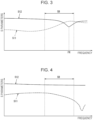
- FIG. 3 An example of a graph of the frequency characteristics of the S parameters of the waveguide 20 for this case is illustrated in FIG. 3 .
- the horizontal axis represents the frequency of an optical signal propagating in the waveguide 20.
- the vertical axis represents the values of S11 and S12.
- the value of S12 is a minimum at the resonance frequency represented by FR. In other words, the transmittance of the signal at the resonance frequency is low.
- SB represents the frequency band of an electrical signal input to the signal wire 43 in order to modulate the optical signal in the optical modulator. If the resonance frequency (FR) is within the frequency band (SB) of the electrical signal input to signal wire 43, the loss of part of the signal modulated by the optical modulator will be large. As a result, the propagation characteristics of the optical modulator will deteriorate.
- the optical modulator 10 includes the adjustment member 30 positioned between the second ground wire 42 and the signal wire 43.
- FIG. 4 An example of a graph of the frequency characteristics of the S parameters of the waveguide 20 for this case is illustrated in FIG. 4 .
- the horizontal axis represents the frequency of an optical signal propagating in the waveguide 20.
- the vertical axis represents the values of S11 and S12.
- the value of S12 does not have a minimum value within the frequency band (SB) of the electrical signal input to the signal wire 43.
- no resonance occurs at least within the frequency band (SB) of the electrical signal.
- the loss of the signal modulated by the optical modulator 10 according to this embodiment is less than the loss of the signal modulated by the optical modulator according to the comparative example.
- the propagation characteristics of the signal modulated in the optical modulator 10 according to this embodiment can be improved.
- the optical modulator 10 can maintain the transmittance of a modulated signal at a high value within the frequency band (SB) of the electrical signal input to the signal wire 43 due to the optical modulator 10 including the adjustment member 30 located between the second ground wire 42 and the signal wire 43. As a result, the propagation characteristics of the modulated signal can be improved.
- SB frequency band
- the adjustment member 30 does not include input/output portions for optical signals. Specifically, the adjustment member 30 does not include parts corresponding to the input portion 21 and the output portion 22 of the waveguide 20. If the adjustment member 30 is assumed to include input/output portions for optical signals, the coupling between the waveguide 20 and the adjustment member 30 can be strengthened. As a result of the coupling between the waveguide 20 and the adjustment member 30 being strengthened, the effect of the adjustment member 30 on the optical signal propagating in the waveguide 20 can become greater. On the other hand, the adjustment member 30 of the optical modulator 10 according to this embodiment does not include input/output portions for optical signals, and therefore the coupling between the waveguide 20 and the adjustment member 30 can be weakened.
- the effect of the adjustment member 30 on the optical signal propagating in the waveguide 20 can become smaller.
- the characteristics of the optical signal modulated in the waveguide 20 can be maintained by reducing the effect of the adjustment member 30.
- the propagation characteristics of the modulated signal can be improved.
- the length of the adjustment member 30 is restricted by the adjustment member 30 including input/output portions for optical signals. As described below, the length of the adjustment member 30 can be adjusted because the adjustment member 30 does not include input/output portions for optical signals.
- an optical signal propagates along the waveguide 20, and an electrical signal propagates along the coplanar line 40.
- the propagation speed of the electrical signal in the coplanar line 40 needs to be matched to the propagation speed of the optical signal in the waveguide 20.
- the difference between the effective refractive index of the waveguide 20 and the effective refractive index of the coplanar line 40 needs to be made small.
- the effective refractive index of the coplanar line 40 can be adjusted by changing the length of the adjustment member 30 in the extension direction thereof (X-axis direction). As illustrated in FIG. 5 , the length of the adjustment member 30 in the extension direction thereof (X-axis direction) can be adjusted by dividing the adjustment member 30 into multiple parts.
- the adjustment member 30 includes an adjustment member 31, an adjustment member 32, ..., and an adjustment member 3n, which are obtained by dividing the adjustment member 30 into n pieces.
- the adjustment member 30 may be shortened without being divided and left as a single adjustment member 30.
- the effective refractive index of the coplanar line 40 is determined in accordance with the ratio of the length of the adjustment member 30 to the length of the waveguide 20.
- the ratio of the length of the adjustment member 30 to the length of the waveguide 20 is also referred to as the filling ratio of the adjustment member 30.
- the filling ratio is calculated by dividing the total length of the adjustment member 30 by the length of the waveguide 20.
- the length of the waveguide 20 is represented by L.
- the respective lengths of the n adjustment members 30 are represented by lengths L1, L2, ..., and Ln.
- the filling ratio of the adjustment members 30 is calculated as (L1 + L2 + ... + Ln)/L.
- the filling ratio of the adjustment member 30 is calculated by dividing the length of the shortened adjustment member 30 by the length of the waveguide 20.
- the lengths of each part of the divided adjustment member 30 is the same as the length in the extension direction.
- the length of each part of the divided adjustment member 30 may be calculated as the length in the extension direction in an orthographic projection on the waveguide 20.
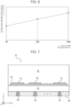
- FIG. 6 illustrates, as a graph, the relationship between the filling ratio of the adjustment member 30 and the effective refractive index of the coplanar line 40.
- the horizontal axis represents the filling ratio of the adjustment member 30.
- the vertical axis represents the effective refractive index of the coplanar line 40. The smaller the filling ratio of the adjustment member 30, the lower the effective refractive index of the coplanar line 40. Therefore, the filling ratio of the adjustment member 30 can be adjusted so that the effective refractive index of the coplanar line 40 comes close to the effective refractive index of the waveguide 20.
- the total length of the adjustment member 30 (filling ratio of the adjustment member 30) can affect the resonance frequency of the optical signal in the waveguide 20.
- the total length of the adjustment member 30 in the direction along the coplanar line 40 (filling ratio of the adjustment member 30) may be set so that the resonance frequency of the optical signal propagating in the waveguide 20 is higher than the frequency band (SB) of the electrical signal propagating in the signal wire 43.
- SB frequency band
- each divided part of the adjustment member 30 may be freely disposed at positions in the X-axis direction.
- the optical modulator 10 may further include temperature adjusting portions 54.
- the temperature adjusting portions 54 may be positioned inside or below the substrate 50.
- the characteristics of the waveguide 20 or the coplanar line 40 may be affected by the temperature of the substrate 50. Therefore, the characteristics of the optical modulator 10 may be stabilized by adjusting the temperature of the substrate 50 using the temperature adjusting portions 54.
- the temperature adjusting portions 54 may include a heat sink, for example.
- the temperature adjusting portions 54 may include a heater that heats the substrate 50.
- the temperature adjusting portions 54 may include a cooling water pipe that cools the substrate 50.
- the temperature adjusting portions 54 may include piping that circulates water at a prescribed temperature to control the temperature of the substrate 50 to a prescribed temperature.
- the adjustment member 30 can absorb part of the optical signal propagating through the waveguide 20 and generate heat. As least some of the divided parts of the adjustment member 30 may be disposed to overlap the temperature adjusting portions 54 in plan view of the substrate 50 (when the substrate 50 is viewed in the positive Z-axis direction), as illustrated in FIG. 7 . In this way, the temperature of the substrate 50 is easily adjusted. As a result, the characteristics of the optical modulator 10 can be stabilized.
- the optical modulator 10 includes the adjustment member 30 in addition to the waveguide 20 positioned along the coplanar line 40, and this allows the resonance frequency of the waveguide 20 to be adjusted to a frequency outside the frequency band of an electrical signal (frequency band of modulated optical signal). As a result, the propagation characteristics of the signal modulated in the optical modulator 10 can be improved.
- the optical modulator 10 may be used in combination with a configuration for transmitting and receiving light.
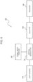
- the optical transceiver 100 includes the optical modulator 10, a light source 110, a signal input portion 120, and an isolator 130.
- the optical transceiver 100 inputs an optical signal from the light source 110 to the optical modulator 10, modulates the light based on a signal input to the signal input portion 120 using the optical modulator 10, and outputs the modulated light from the optical modulator 10 to a receiver 140 via the isolator 130.
- the isolator 130 is configured so that the transmittance of the optical signal propagating from the light source 110 to the receiver 140 is greater than the transmittance of the optical signal propagating from the receiver 140 to the light source 110. Therefore, optical signals will be less likely to enter the light source 110. As a result, the light source 110 can be protected.
- the light source 110 may include, for example, a semiconductor laser such as an LD (laser diode) or a VCSEL (vertical cavity surface emitting laser).
- the light source 110 may include a device that emits optical signals of various wavelengths, not limited to visible light.
- the light source 110 may be formed together with the optical modulator 10 on the substrate 50.
- the optical modulator 10 modulates the light by changing the intensity of the light input from the light source 110 to the waveguide 20 in accordance with a signal input from the signal input portion 120 to the signal wire 43 of the coplanar line 40.
- the optical modulator 10 may be positioned between the isolator 130 and the receiver 140, rather than between the light source 110 and the isolator 130.
- the optical modulator 10 may pulse-modulate the optical signal, for example.
- the signal input portion 120 accepts input of signals from external devices, etc.
- the signal input portion 120 may include a D/A converter, for example.
- the signal input portion 120 outputs a signal to the signal wire 43 of the coplanar line 40 of the optical modulator 10.
- first”, “second”, and so on are identifiers used to distinguish between such configurations.
- “first”, “second”, and so on used to distinguish between the configurations in the present disclosure may be exchanged with each other.
- identifiers “first” and “second” may be exchanged between the first ground wire 41 and the second ground wire 42. Exchanging of the identifiers take places simultaneously. Even after exchanging the identifiers, the configurations are distinguishable from each other.
- the identifiers may be deleted. The configurations that have had their identifiers deleted are distinguishable from each other by symbols. Just the use of identifiers such as “first” and “second” in this disclosure is not to be used as a basis for interpreting the order of such configurations or the existence of identifiers with smaller numbers.
- the X-axis, the Y-axis, and the Z-axis are provided for convenience of explanation, but may be interchanged with each other.
- the configurations of the present disclosure have been described using a Cartesian coordinate system consisting of a X-axis, a Y-axis, and a Z-axis.
- the positional relationship of each configuration in the present disclosure is not limited to a Cartesian relationship.
Landscapes
- Physics & Mathematics (AREA)
- Nonlinear Science (AREA)
- General Physics & Mathematics (AREA)
- Optics & Photonics (AREA)
- Electromagnetism (AREA)
- Chemical & Material Sciences (AREA)
- Engineering & Computer Science (AREA)
- Ceramic Engineering (AREA)
- Crystallography & Structural Chemistry (AREA)
- Optical Modulation, Optical Deflection, Nonlinear Optics, Optical Demodulation, Optical Logic Elements (AREA)
- Optical Couplings Of Light Guides (AREA)
- Optical Integrated Circuits (AREA)
Abstract
An optical modulator includes: a substrate; a coplanar line, on the substrate, including a first ground wire, a second ground wire, and a signal wire, between the first ground wire and the second ground wire, coupled to each of the first ground wire and the second ground wire; a waveguide, between the first ground wire and the signal wire along the coplanar line on the substrate in plan view of the substrate, including an input portion and an output portion for an optical signal, the output portion configured to output an optical signal input from the input portion and modulated using a signal that propagates along the coplanar line; and an adjustment member, between the second ground wire and the signal wire along the coplanar line on the substrate in plan view of the substrate, not including an input portion or an output portion for an optical signal.
Description
- This application claims priority of
Japanese Patent Application No. 2022-116739 (filed July 21, 2022 - The present disclosure relates to an optical modulator and an optical transceiver.
- In a known structure, a single optical waveguide is positioned between one of the ground wires and a common signal wire of a coplanar line, whereas no optical waveguide is positioned between the other ground wire and the common signal wire of the coplanar line (for example, refer to Fig. 1A of Non Patent Literature 1).
- Non Patent Literature 1: Jianfeng Ding, Hongtao Chen, Lin Yang, Lei Zhang, Ruiqiang Ji, Yonghui Tian, Weiwei Zhu, Yangyang Lu, Ping Zhou, Rui Min, and Mingbin Yu, Ultra-low-power carrier-depletion Mach-Zehnder silicon optical modulator, Optics Express, Vol. 20, No. 7 (2012)
- In an embodiment of the present disclosure, an optical modulator includes a substrate, a coplanar line, a waveguide, and an adjustment member. The coplanar line is positioned on the substrate and includes a first ground wire, a second ground wire, and a signal wire. The signal wire is positioned between the first ground wire and the second ground wire and is coupled to each of the first ground wire and the second ground wire. The waveguide is positioned between the first ground wire and the signal wire along the coplanar line on the substrate in plan view of the substrate. The waveguide includes an input portion and an output portion for an optical signal. The output portion is configured to output an optical signal input from the input portion and modulated by a signal propagating along the coplanar line. The adjustment member is positioned between the second ground wire and the signal wire along the coplanar line on the substrate in plan view of the substrate. The adjustment member does not include an input portion or an output portion for an optical signal.
- In an embodiment of the present disclosure, an optical transceiver includes an optical modulator and a light source. The light source is configured to input an optical signal to the optical modulator. The optical modulator includes a substrate, a coplanar line positioned on the substrate, a waveguide, and an adjustment member. The coplanar line includes a first ground wire, a second ground wire, and a signal wire. The signal wire is positioned between the first ground wire and the second ground wire and is coupled to each of the first ground wire and the second ground wire. The waveguide is positioned between the first ground wire and the signal wire along the coplanar line on the substrate in plan view of the substrate. The waveguide includes an input portion and an output portion for an optical signal. The output portion is configured to output an optical signal input from the input portion and modulated by a signal propagating along the coplanar line. The adjustment member is positioned between the second ground wire and the signal wire along the coplanar line on the substrate in plan view of the substrate. The adjustment member does not include an input portion or an output portion for an optical signal.
-
-
FIG. 1 is a plan view illustrating an example configuration of an optical modulator according to an embodiment. -
FIG. 2 is a sectional view taken along line A-A inFIG. 1 . -
FIG. 3 is a graph illustrating the frequency characteristics of the S parameters of an optical modulator according to a comparative example. -
FIG. 4 is a graph illustrating an example of the frequency characteristics of the S parameters of the optical modulator according to this embodiment. -
FIG. 5 is a plan view illustrating an example configuration in which an adjustment member is divided into parts and then disposed. -
FIG. 6 is a graph illustrating an example of the relationship between the filling ratio of an adjustment member and the effective refractive index of a coplanar line. -
FIG. 7 is a sectional view taken along line B-B inFIG. 5 . -
FIG. 8 is a block diagram illustrating an example configuration of an optical transceiver according to an embodiment. - When an optical waveguide is positioned at the side of one ground wire and not at the side of another ground wire in a coplanar line, the propagation efficiency of an optical signal propagating in the optical waveguide will decrease due to resonance. The propagation efficiency of optical signals in optical waveguides needs to be improved. In an embodiment of the present disclosure, an optical modulator and an optical transceiver can have improved propagation efficiency for optical signals.
- As illustrated in
FIGs. 1 and 2 , in an embodiment, anoptical modulator 10 includes acoplanar line 40, awaveguide 20, anadjustment member 30, and asubstrate 50. Theoptical modulator 10 is assumed to be held by thesubstrate 50. Theoptical modulator 10 further includes a firstdielectric layer 51 and a seconddielectric layer 52 positioned on thesubstrate 50. Theoptical modulator 10 further includes asemiconductor layer 53 positioned on the firstdielectric layer 51. - The
coplanar line 40 includes afirst ground wire 41 and asecond ground wire 42, which are grounded, and asignal wire 43 to which an electrical signal is input. Thefirst ground wire 41, thesecond ground wire 42, and thesignal wire 43 extend in an X-axis direction. Thefirst ground wire 41 is electrically connected to thesemiconductor layer 53 through viawiring lines 411. Thesecond ground wire 42 is electrically connected to thesemiconductor layer 53 through viawiring lines 421. Thesignal wire 43 is electrically connected to thesemiconductor layer 53 through viawiring lines 431. Thefirst ground wire 41, thesecond ground wire 42, and thesignal wire 43 are insulated from each other by the seconddielectric layer 52. Thesignal wire 43 is positioned between thefirst ground wire 41 and thesecond ground wire 42. Thesignal wire 43 is electrically coupled to each of thefirst ground wire 41 and thesecond ground wire 42. - The
waveguide 20 extends in the X-axis direction on thesemiconductor layer 53. Thewaveguide 20 is electrically connected to thesemiconductor layer 53. Thewaveguide 20 is positioned between thefirst ground wire 41 and thesignal wire 43 of thecoplanar line 40. Thewaveguide 20 is electrically connected to thefirst ground wire 41 on the positive Y-axis direction side and is electrically connected to thesignal wire 43 on the negative Y-axis direction side in a sectional view (seeFIG. 2 ) taken along a plane (YZ plane) perpendicular to the direction in which thewaveguide 20 extends (X-axis direction). As a result, an electrical signal between thesignal wire 43 and thefirst ground wire 41 is applied to thewaveguide 20 in a direction that intersects thewaveguide 20 in the direction in which thewaveguide 20 extends (X-axis direction). - The
waveguide 20 includes aninput portion 21 and anoutput portion 22. An optical signal input from theinput portion 21 propagates through thewaveguide 20 and is output from theoutput portion 22. The optical signal is affected by the electrical signal applied to thewaveguide 20 by thefirst ground wire 41 and thesignal wire 43 while propagating through thewaveguide 20, which is positioned between thefirst ground wire 41 and thesignal wire 43. The amplitude of the optical signal changes due to the effect of the electrical signal while the optical signal propagates through thewaveguide 20. In other words, the optical signal is modulated by the electrical signal propagating along thecoplanar line 40 and is then output from theoutput portion 22. - The
adjustment member 30 extends in the X-axis direction on thesemiconductor layer 53. Theadjustment member 30 may be electrically connected to thesemiconductor layer 53 or insulated from thesemiconductor layer 53. Theadjustment member 30 is positioned between thesecond ground wire 42 and thesignal wire 43 of thecoplanar line 40. - In this embodiment, the
substrate 50 is assumed to contain silicon (Si), but is not limited to this material and may contain another semiconductor material such as GaAs. Thesubstrate 50 may contain a conductor such as metal or a dielectric such as glass or resin. Thesubstrate 50 may contain various other materials, not limited to these examples. - The
first dielectric layer 51 is assumed to contain a silicon oxide film (SiO2), but may also contain various other dielectric or insulating materials. - The
second dielectric layer 52 is assumed to contain a silicon oxide film (SiO2), but may also contain various other dielectric or insulating materials. Thesecond dielectric layer 52 may contain a gas such as air, or may be configured as a vacuum. - The
semiconductor layer 53 is assumed to contain silicon (Si). Thesemiconductor layer 53 may contain a material obtained by injecting a dopant into a semiconductor. Thesemiconductor layer 53 may be replaced with a layer of a conductor such as a metal. - The
first ground wire 41, thesecond ground wire 42, and thesignal wire 43 may contain a metal such as aluminum, but are not limited to this material and may contain various conductor materials. The viawiring lines - The
waveguide 20 and theadjustment member 30 are assumed to contain silicon (Si), but are limited to this material and may contain various other dielectric materials. Thewaveguide 20 and theadjustment member 30 may contain the same material as each other or different materials. - Part of the
waveguide 20 is surrounded by thesecond dielectric layer 52. The material of thewaveguide 20 is assumed to be determined so that the relative dielectric constant of thewaveguide 20 is greater than the relative dielectric constant of thesecond dielectric layer 52. In other words, the materials of thewaveguide 20 and thesecond dielectric layer 52 are determined so that the refractive index of thesecond dielectric layer 52 is greater than the refractive index of thewaveguide 20. As a result, an optical signal propagating in thewaveguide 20 can be totally reflected at the boundary with thesecond dielectric layer 52. As a result, loss of the optical signal propagating in thewaveguide 20 can be reduced. - The
waveguide 20 is configured so that thesignal wire 43 and thefirst ground wire 41 are not short-circuited by thewaveguide 20. In other words, thewaveguide 20 may be configured so that the resistance value between the side that is connected to thesignal wire 43 via the viawiring lines 431 and thesemiconductor layer 53 and the side that is connected to thefirst ground wire 41 via the viawiring lines 411 and thesemiconductor layer 53 is equal to or greater than a prescribed value. The resistance value may be adjusted, for example, by changing the dopant density of the semiconductor contained in thewaveguide 20, or by changing the electrical resistance between thewaveguide 20 and thecoplanar line 40. - In this embodiment, the
waveguide 20 is assumed to include an n-type semiconductor positioned on the side connected to thesignal wire 43 and a p-type semiconductor positioned on the side connected to thefirst ground wire 41. The n-type semiconductor and the p-type semiconductor extend along the direction in which thewaveguide 20 extends (X-axis direction), and are positioned side by side in a direction that intersects the direction in which thewaveguide 20 extends (Y-axis direction). Thewaveguide 20 includes a pn junction in which an n-type semiconductor and a p-type semiconductor are bonded to each other. The pn junction part is positioned along the direction (X-axis direction) in which thewaveguide 20 extends. Thewaveguide 20 is configured so that the bias is a reverse direction bias when a positive potential with respect to the ground potential of thefirst ground wire 41 is applied to thesignal wire 43 due to the presence of the pn junction. As a result, thewaveguide 20 is configured so that a short-circuit does not occur between thesignal wire 43 and thefirst ground wire 41 when the potential of thesignal wire 43 is a positive potential with respect to the ground potential of thefirst ground wire 41. - The
adjustment member 30 may be configured to include the same pn junction as thewaveguide 20, or may be configured using just an n-type semiconductor, a p-type semiconductor, or an intrinsic semiconductor. - As described above, the
optical modulator 10 modulates the light input from theinput portion 21 to thewaveguide 20 by applying an electrical signal to thecoplanar line 40, and then outputs the modulated light from theoutput portion 22. If a line made up of pair of wires consisting of one ground wire and one signal wire is used instead of thecoplanar line 40, the signal radiation will be greater. In this embodiment, theoptical modulator 10 can reduce signal radiation by using thecoplanar line 40. In other words, signal loss can be reduced by using thecoplanar line 40. - The propagation characteristics of the
waveguide 20 of theoptical modulator 10 are expressed as the frequency characteristics of S parameters (scattering parameters). The S parameters of thewaveguide 20 include S12 representing the ratio of light transmitted from theinput portion 21 to theoutput portion 22, and S11 representing the ratio of light input to theinput portion 21, reflected within thewaveguide 20, and returning to theinput portion 21. In other words, the S parameters of thewaveguide 20 include the transmittance and reflectance of the light input to thewaveguide 20. - Out of the light propagating in the
waveguide 20, light of a prescribed frequency may resonate inside thewaveguide 20 and experience significant loss. The prescribed frequency at which light resonates is also referred to as the resonance frequency. The resonance frequency changes in accordance with the shape of thewaveguide 20. For example, the longer the line length of thewaveguide 20, the lower the resonance frequency of thewaveguide 20. - The
waveguide 20 can be expressed by an equivalent circuit that includes a capacitor and an inductor. The resonance frequency of thewaveguide 20 can be assigned to the equivalent circuit of thewaveguide 20. The equivalent circuit of thewaveguide 20 is affected by the arrangement of electrodes or dielectrics around thewaveguide 20. Therefore, the resonance frequency changes depending on the arrangement of the electrodes or dielectrics around thewaveguide 20. - As a comparative example, an optical modulator is assumed in which the
waveguide 20 is positioned between thefirst ground wire 41 and thesignal wire 43, but not between thesecond ground wire 42 and thesignal wire 43. An example of a graph of the frequency characteristics of the S parameters of thewaveguide 20 for this case is illustrated inFIG. 3 . In the graph inFIG. 3 , the horizontal axis represents the frequency of an optical signal propagating in thewaveguide 20. The vertical axis represents the values of S11 and S12. The value of S12 is a minimum at the resonance frequency represented by FR. In other words, the transmittance of the signal at the resonance frequency is low. Here, SB represents the frequency band of an electrical signal input to thesignal wire 43 in order to modulate the optical signal in the optical modulator. If the resonance frequency (FR) is within the frequency band (SB) of the electrical signal input to signalwire 43, the loss of part of the signal modulated by the optical modulator will be large. As a result, the propagation characteristics of the optical modulator will deteriorate. - On the other hand, in this embodiment, the
optical modulator 10 includes theadjustment member 30 positioned between thesecond ground wire 42 and thesignal wire 43. An example of a graph of the frequency characteristics of the S parameters of thewaveguide 20 for this case is illustrated inFIG. 4 . In the graph inFIG. 4 , the horizontal axis represents the frequency of an optical signal propagating in thewaveguide 20. The vertical axis represents the values of S11 and S12. The value of S12 does not have a minimum value within the frequency band (SB) of the electrical signal input to thesignal wire 43. In other words, in theoptical modulator 10 according to this embodiment, no resonance occurs at least within the frequency band (SB) of the electrical signal. Therefore, the loss of the signal modulated by theoptical modulator 10 according to this embodiment is less than the loss of the signal modulated by the optical modulator according to the comparative example. As a result, the propagation characteristics of the signal modulated in theoptical modulator 10 according to this embodiment can be improved. - As described above, in this embodiment, the
optical modulator 10 can maintain the transmittance of a modulated signal at a high value within the frequency band (SB) of the electrical signal input to thesignal wire 43 due to theoptical modulator 10 including theadjustment member 30 located between thesecond ground wire 42 and thesignal wire 43. As a result, the propagation characteristics of the modulated signal can be improved. - In addition, in the
optical modulator 10 according to this embodiment, theadjustment member 30 does not include input/output portions for optical signals. Specifically, theadjustment member 30 does not include parts corresponding to theinput portion 21 and theoutput portion 22 of thewaveguide 20. If theadjustment member 30 is assumed to include input/output portions for optical signals, the coupling between thewaveguide 20 and theadjustment member 30 can be strengthened. As a result of the coupling between thewaveguide 20 and theadjustment member 30 being strengthened, the effect of theadjustment member 30 on the optical signal propagating in thewaveguide 20 can become greater. On the other hand, theadjustment member 30 of theoptical modulator 10 according to this embodiment does not include input/output portions for optical signals, and therefore the coupling between thewaveguide 20 and theadjustment member 30 can be weakened. Due to the weakening of the coupling between thewaveguide 20 and theadjustment member 30, the effect of theadjustment member 30 on the optical signal propagating in thewaveguide 20 can become smaller. The characteristics of the optical signal modulated in thewaveguide 20 can be maintained by reducing the effect of theadjustment member 30. As a result, the propagation characteristics of the modulated signal can be improved. In addition, the length of theadjustment member 30 is restricted by theadjustment member 30 including input/output portions for optical signals. As described below, the length of theadjustment member 30 can be adjusted because theadjustment member 30 does not include input/output portions for optical signals. - In the
optical modulator 10, an optical signal propagates along thewaveguide 20, and an electrical signal propagates along thecoplanar line 40. In order to efficiently modulate the optical signal using the electrical signal, the propagation speed of the electrical signal in thecoplanar line 40 needs to be matched to the propagation speed of the optical signal in thewaveguide 20. In order to match the propagation speed of the electrical signal to the propagation speed of the optical signal, the difference between the effective refractive index of thewaveguide 20 and the effective refractive index of thecoplanar line 40 needs to be made small. - The effective refractive index of the
coplanar line 40 can be adjusted by changing the length of theadjustment member 30 in the extension direction thereof (X-axis direction). As illustrated inFIG. 5 , the length of theadjustment member 30 in the extension direction thereof (X-axis direction) can be adjusted by dividing theadjustment member 30 into multiple parts. InFIG. 5 , theadjustment member 30 includes anadjustment member 31, anadjustment member 32, ..., and anadjustment member 3n, which are obtained by dividing theadjustment member 30 into n pieces. Theadjustment member 30 may be shortened without being divided and left as asingle adjustment member 30. - The effective refractive index of the
coplanar line 40 is determined in accordance with the ratio of the length of theadjustment member 30 to the length of thewaveguide 20. The ratio of the length of theadjustment member 30 to the length of thewaveguide 20 is also referred to as the filling ratio of theadjustment member 30. The filling ratio is calculated by dividing the total length of theadjustment member 30 by the length of thewaveguide 20. The length of thewaveguide 20 is represented by L. The respective lengths of then adjustment members 30 are represented by lengths L1, L2, ..., and Ln. In this case, the filling ratio of theadjustment members 30 is calculated as (L1 + L2 + ... + Ln)/L. When oneadjustment member 30 is shortened, the filling ratio of theadjustment member 30 is calculated by dividing the length of the shortenedadjustment member 30 by the length of thewaveguide 20. - When the
adjustment member 30 is divided along a plane perpendicular to the extension direction thereof, the lengths of each part of the dividedadjustment member 30 is the same as the length in the extension direction. When theadjustment member 30 is divided along a plane that is tilted from a plane perpendicular to the extension direction of theadjustment member 30, the length of each part of the dividedadjustment member 30 may be calculated as the length in the extension direction in an orthographic projection on thewaveguide 20. -
FIG. 6 illustrates, as a graph, the relationship between the filling ratio of theadjustment member 30 and the effective refractive index of thecoplanar line 40. In the graph inFIG. 6 , the horizontal axis represents the filling ratio of theadjustment member 30. The vertical axis represents the effective refractive index of thecoplanar line 40. The smaller the filling ratio of theadjustment member 30, the lower the effective refractive index of thecoplanar line 40. Therefore, the filling ratio of theadjustment member 30 can be adjusted so that the effective refractive index of thecoplanar line 40 comes close to the effective refractive index of thewaveguide 20. - The total length of the adjustment member 30 (filling ratio of the adjustment member 30) can affect the resonance frequency of the optical signal in the
waveguide 20. The total length of theadjustment member 30 in the direction along the coplanar line 40 (filling ratio of the adjustment member 30) may be set so that the resonance frequency of the optical signal propagating in thewaveguide 20 is higher than the frequency band (SB) of the electrical signal propagating in thesignal wire 43. Thus, the loss of the signal modulated in accordance with the electrical signal is reduced. As a result, the propagation characteristics of the signal modulated in theoptical modulator 10 can be improved. - When the
adjustment member 30 is divided into multiple parts, the effect of the arrangement, in the X-axis direction, of each divided part on the effective refractive index of thecoplanar line 40 is small. Therefore, each divided part of theadjustment member 30 may be freely disposed at positions in the X-axis direction. - As illustrated in
FIG. 7 , theoptical modulator 10 may further includetemperature adjusting portions 54. Thetemperature adjusting portions 54 may be positioned inside or below thesubstrate 50. The characteristics of thewaveguide 20 or thecoplanar line 40 may be affected by the temperature of thesubstrate 50. Therefore, the characteristics of theoptical modulator 10 may be stabilized by adjusting the temperature of thesubstrate 50 using thetemperature adjusting portions 54. - The
temperature adjusting portions 54 may include a heat sink, for example. Thetemperature adjusting portions 54 may include a heater that heats thesubstrate 50. Thetemperature adjusting portions 54 may include a cooling water pipe that cools thesubstrate 50. Thetemperature adjusting portions 54 may include piping that circulates water at a prescribed temperature to control the temperature of thesubstrate 50 to a prescribed temperature. - In the
optical modulator 10, theadjustment member 30 can absorb part of the optical signal propagating through thewaveguide 20 and generate heat. As least some of the divided parts of theadjustment member 30 may be disposed to overlap thetemperature adjusting portions 54 in plan view of the substrate 50 (when thesubstrate 50 is viewed in the positive Z-axis direction), as illustrated inFIG. 7 . In this way, the temperature of thesubstrate 50 is easily adjusted. As a result, the characteristics of theoptical modulator 10 can be stabilized. - As described above, in this embodiment, the
optical modulator 10 includes theadjustment member 30 in addition to thewaveguide 20 positioned along thecoplanar line 40, and this allows the resonance frequency of thewaveguide 20 to be adjusted to a frequency outside the frequency band of an electrical signal (frequency band of modulated optical signal). As a result, the propagation characteristics of the signal modulated in theoptical modulator 10 can be improved. - The
optical modulator 10 may be used in combination with a configuration for transmitting and receiving light. As illustrated inFIG. 8 , theoptical transceiver 100 includes theoptical modulator 10, alight source 110, asignal input portion 120, and anisolator 130. Theoptical transceiver 100 inputs an optical signal from thelight source 110 to theoptical modulator 10, modulates the light based on a signal input to thesignal input portion 120 using theoptical modulator 10, and outputs the modulated light from theoptical modulator 10 to areceiver 140 via theisolator 130. Theisolator 130 is configured so that the transmittance of the optical signal propagating from thelight source 110 to thereceiver 140 is greater than the transmittance of the optical signal propagating from thereceiver 140 to thelight source 110. Therefore, optical signals will be less likely to enter thelight source 110. As a result, thelight source 110 can be protected. - The
light source 110 may include, for example, a semiconductor laser such as an LD (laser diode) or a VCSEL (vertical cavity surface emitting laser). Thelight source 110 may include a device that emits optical signals of various wavelengths, not limited to visible light. Thelight source 110 may be formed together with theoptical modulator 10 on thesubstrate 50. - The
optical modulator 10 modulates the light by changing the intensity of the light input from thelight source 110 to thewaveguide 20 in accordance with a signal input from thesignal input portion 120 to thesignal wire 43 of thecoplanar line 40. Theoptical modulator 10 may be positioned between the isolator 130 and thereceiver 140, rather than between thelight source 110 and theisolator 130. Theoptical modulator 10 may pulse-modulate the optical signal, for example. Thesignal input portion 120 accepts input of signals from external devices, etc. Thesignal input portion 120 may include a D/A converter, for example. Thesignal input portion 120 outputs a signal to thesignal wire 43 of thecoplanar line 40 of theoptical modulator 10. - Although embodiments of the present disclosure have been described based on the drawings and examples, please note that one skilled in the art can make various variations or changes based on the present disclosure. Please note that, therefore, these variations or changes are included within the scope of the present disclosure. For example, the functions included in each component can be rearranged in a logically consistent manner, and a plurality of components can be combined into a single component or a single component can be divided into a plurality of components. Please understand that the scope of the present disclosure also includes these forms.
- In the present disclosure, "first", "second", and so on are identifiers used to distinguish between such configurations. Regarding the configurations, "first", "second", and so on used to distinguish between the configurations in the present disclosure may be exchanged with each other. For example, identifiers "first" and "second" may be exchanged between the
first ground wire 41 and thesecond ground wire 42. Exchanging of the identifiers take places simultaneously. Even after exchanging the identifiers, the configurations are distinguishable from each other. The identifiers may be deleted. The configurations that have had their identifiers deleted are distinguishable from each other by symbols. Just the use of identifiers such as "first" and "second" in this disclosure is not to be used as a basis for interpreting the order of such configurations or the existence of identifiers with smaller numbers. - In the present disclosure, the X-axis, the Y-axis, and the Z-axis are provided for convenience of explanation, but may be interchanged with each other. The configurations of the present disclosure have been described using a Cartesian coordinate system consisting of a X-axis, a Y-axis, and a Z-axis. The positional relationship of each configuration in the present disclosure is not limited to a Cartesian relationship.
-
- 10 optical modulator
- 20 waveguide (21: input portion, 22: output portion)
- 30, 31, 32, 3n adjustment member
- 40 coplanar line (41: first ground wire, 42: second ground wire, 43: signal wire)
- 50 substrate (51, 52: dielectric layer, 53: semiconductor layer, 54: temperature adjusting portion)
- 100 optical transceiver (110: light source, 120: signal input portion, 130: isolator, 140: receiver)
Claims (6)
- An optical modulator comprising:a substrate;a coplanar line positioned on the substrate and including a first ground wire, a second ground wire, and a signal wire positioned between the first ground wire and the second ground wire and coupled to each of the first ground wire and the second ground wire;a waveguide positioned between the first ground wire and the signal wire along the coplanar line on the substrate in plan view of the substrate, and including an input portion and an output portion for an optical signal, the output portion configured to output an optical signal input from the input portion and modulated using a signal that propagates along the coplanar line; andan adjustment member positioned between the second ground wire and the signal wire along the coplanar line on the substrate in plan view of the substrate, and not including an input portion or an output portion for an optical signal.
- The optical modulator according to claim 1, wherein the adjustment member is shorter than the waveguide in a direction along the coplanar line.
- The optical modulator according to claim 2, wherein the adjustment member is divided into multiple parts.
- The optical modulator according to claim 3, further comprising:a temperature adjusting portion positioned inside or below the substrate,wherein at least part of the divided parts of the adjustment member is positioned overlapping the temperature adjusting portion in plan view of the substrate.
- The optical modulator according to any one of claims 2 to 4, wherein a total length of the adjustment member in the direction along the coplanar line is set so that a resonance frequency of an optical signal propagating in the waveguide is higher than a frequency band of a signal propagating in the signal wire.
- An optical transceiver comprising:an optical modulator; anda light source configured to input an optical signal to the optical modulator,wherein the optical modulator includesa substrate,a coplanar line positioned on the substrate and including a first ground wire, a second ground wire, and a signal wire positioned between the first ground wire and the second ground wire and coupled to each of the first ground wire and the second ground wire,a waveguide positioned between the first ground wire and the signal wire along the coplanar line on the substrate in plan view of the substrate, and including an input portion and an output portion for an optical signal, the output portion configured to output an optical signal input from the input portion and modulated using a signal that propagates along the coplanar line, andan adjustment member positioned between the second ground wire and the signal wire along the coplanar line on the substrate in plan view of the substrate, and not including an input portion or an output portion for an optical signal.
Applications Claiming Priority (2)
| Application Number | Priority Date | Filing Date | Title |
|---|---|---|---|
| JP2022116739A JP7723645B2 (en) | 2022-07-21 | 2022-07-21 | Optical modulator and optical transceiver |
| PCT/JP2023/025334 WO2024018935A1 (en) | 2022-07-21 | 2023-07-07 | Optical modulator and optical transceiver |
Publications (1)
| Publication Number | Publication Date |
|---|---|
| EP4560387A1 true EP4560387A1 (en) | 2025-05-28 |
Family
ID=89617911
Family Applications (1)
| Application Number | Title | Priority Date | Filing Date |
|---|---|---|---|
| EP23842860.1A Pending EP4560387A1 (en) | 2022-07-21 | 2023-07-07 | Optical modulator and optical transceiver |
Country Status (5)
| Country | Link |
|---|---|
| US (1) | US20260016711A1 (en) |
| EP (1) | EP4560387A1 (en) |
| JP (1) | JP7723645B2 (en) |
| CN (1) | CN119585668A (en) |
| WO (1) | WO2024018935A1 (en) |
Family Cites Families (5)
| Publication number | Priority date | Publication date | Assignee | Title |
|---|---|---|---|---|
| JPS5232347A (en) * | 1975-09-08 | 1977-03-11 | Nippon Telegr & Teleph Corp <Ntt> | Wave guide light modulator |
| US8380016B1 (en) * | 2009-06-09 | 2013-02-19 | University Of Washington Through Its Center For Commercialization | Geometries for electrooptic modulation with χ2 materials in silicon waveguides |
| JP2017207552A (en) * | 2016-05-16 | 2017-11-24 | 株式会社フジクラ | Substrate-type optical waveguide and substrate-type optical modulator |
| JP2018105975A (en) * | 2016-12-26 | 2018-07-05 | 株式会社フジクラ | Light modulation element |
| CN112379538B (en) * | 2020-11-17 | 2023-05-09 | 中国电子科技集团公司第三十八研究所 | Coplanar stripline traveling wave electrode and silicon-based Mach-Zehnder modulator |
-
2022
- 2022-07-21 JP JP2022116739A patent/JP7723645B2/en active Active
-
2023
- 2023-07-07 WO PCT/JP2023/025334 patent/WO2024018935A1/en not_active Ceased
- 2023-07-07 CN CN202380054874.2A patent/CN119585668A/en active Pending
- 2023-07-07 US US18/993,711 patent/US20260016711A1/en active Pending
- 2023-07-07 EP EP23842860.1A patent/EP4560387A1/en active Pending
Also Published As
| Publication number | Publication date |
|---|---|
| CN119585668A (en) | 2025-03-07 |
| US20260016711A1 (en) | 2026-01-15 |
| JP7723645B2 (en) | 2025-08-14 |
| JP2024014128A (en) | 2024-02-01 |
| WO2024018935A1 (en) | 2024-01-25 |
Similar Documents
| Publication | Publication Date | Title |
|---|---|---|
| US9448425B2 (en) | Optical waveguide element and optical modulator | |
| US8649639B2 (en) | Method and system for waveguide mode filters | |
| US10027089B2 (en) | Coupled ring resonator system | |
| EP2905639B1 (en) | Shielding regions for photonic integrated circuits | |
| US20230288633A1 (en) | Isolator and isolator manufacturing method | |
| US10976564B2 (en) | Isolator, light source device, optical transmitter, and optical amplifier | |
| JP7636497B2 (en) | Isolator | |
| JP7435097B2 (en) | Optical waveguide elements and optical waveguide devices | |
| US11294208B2 (en) | Optical device | |
| EP4560387A1 (en) | Optical modulator and optical transceiver | |
| JP7630738B1 (en) | Optical Integrated Circuit | |
| US12111522B2 (en) | Isolator, light source apparatus, optical transceiver, optical switch, optical amplifier, and data center | |
| JP2022506323A (en) | Externally reflected return light resistant laser | |
| US12535638B2 (en) | Multi-step waveguide tapering to couple light from a light source to a ridge waveguide | |
| JP5416658B2 (en) | Optical modulator and optical modulator module | |
| KR100493089B1 (en) | Integrated optical device | |
| US12142807B2 (en) | High-frequency package including a substrate body having first and second coplanar lines on opposite surfaces thereof connected by a pseudo coaxial line with exposed portions therein | |
| WO2025083816A1 (en) | Optical integrated circuit | |
| WO2025079267A1 (en) | Isolator | |
| CN118409392A (en) | Optical waveguide element, optical modulation device using the optical waveguide element, and optical transmission device | |
| JP2010266509A (en) | Method of designing optical coupling circuit, and optical coupling circuit |
Legal Events
| Date | Code | Title | Description |
|---|---|---|---|
| STAA | Information on the status of an ep patent application or granted ep patent |
Free format text: STATUS: THE INTERNATIONAL PUBLICATION HAS BEEN MADE |
|
| PUAI | Public reference made under article 153(3) epc to a published international application that has entered the european phase |
Free format text: ORIGINAL CODE: 0009012 |
|
| STAA | Information on the status of an ep patent application or granted ep patent |
Free format text: STATUS: REQUEST FOR EXAMINATION WAS MADE |
|
| 17P | Request for examination filed |
Effective date: 20250103 |
|
| AK | Designated contracting states |
Kind code of ref document: A1 Designated state(s): AL AT BE BG CH CY CZ DE DK EE ES FI FR GB GR HR HU IE IS IT LI LT LU LV MC ME MK MT NL NO PL PT RO RS SE SI SK SM TR |
|
| DAV | Request for validation of the european patent (deleted) | ||
| DAX | Request for extension of the european patent (deleted) |