EP4557506A1 - Antenna module - Google Patents
Antenna module Download PDFInfo
- Publication number
- EP4557506A1 EP4557506A1 EP24208909.2A EP24208909A EP4557506A1 EP 4557506 A1 EP4557506 A1 EP 4557506A1 EP 24208909 A EP24208909 A EP 24208909A EP 4557506 A1 EP4557506 A1 EP 4557506A1
- Authority
- EP
- European Patent Office
- Prior art keywords
- substrate
- heat dissipation
- dissipation structure
- antenna module
- mounting surface
- Prior art date
- Legal status (The legal status is an assumption and is not a legal conclusion. Google has not performed a legal analysis and makes no representation as to the accuracy of the status listed.)
- Pending
Links
Images




Classifications
-
- H—ELECTRICITY
- H01—ELECTRIC ELEMENTS
- H01Q—ANTENNAS, i.e. RADIO AERIALS
- H01Q1/00—Details of, or arrangements associated with, antennas
- H01Q1/02—Arrangements for de-icing; Arrangements for drying-out ; Arrangements for cooling; Arrangements for preventing corrosion
-
- H—ELECTRICITY
- H01—ELECTRIC ELEMENTS
- H01Q—ANTENNAS, i.e. RADIO AERIALS
- H01Q1/00—Details of, or arrangements associated with, antennas
- H01Q1/12—Supports; Mounting means
- H01Q1/22—Supports; Mounting means by structural association with other equipment or articles
- H01Q1/2283—Supports; Mounting means by structural association with other equipment or articles mounted in or on the surface of a semiconductor substrate as a chip-type antenna or integrated with other components into an IC package
-
- H—ELECTRICITY
- H01—ELECTRIC ELEMENTS
- H01Q—ANTENNAS, i.e. RADIO AERIALS
- H01Q1/00—Details of, or arrangements associated with, antennas
- H01Q1/52—Means for reducing coupling between antennas; Means for reducing coupling between an antenna and another structure
- H01Q1/526—Electromagnetic shields
-
- H—ELECTRICITY
- H01—ELECTRIC ELEMENTS
- H01Q—ANTENNAS, i.e. RADIO AERIALS
- H01Q21/00—Antenna arrays or systems
- H01Q21/0006—Particular feeding systems
- H01Q21/0025—Modular arrays
-
- H—ELECTRICITY
- H01—ELECTRIC ELEMENTS
- H01Q—ANTENNAS, i.e. RADIO AERIALS
- H01Q21/00—Antenna arrays or systems
- H01Q21/06—Arrays of individually energised antenna units similarly polarised and spaced apart
- H01Q21/20—Arrays of individually energised antenna units similarly polarised and spaced apart the units being spaced along or adjacent to a curvilinear path
- H01Q21/205—Arrays of individually energised antenna units similarly polarised and spaced apart the units being spaced along or adjacent to a curvilinear path providing an omnidirectional coverage
-
- H—ELECTRICITY
- H01—ELECTRIC ELEMENTS
- H01Q—ANTENNAS, i.e. RADIO AERIALS
- H01Q25/00—Antennas or antenna systems providing at least two radiating patterns
- H01Q25/005—Antennas or antenna systems providing at least two radiating patterns providing two patterns of opposite direction; back to back antennas
-
- H—ELECTRICITY
- H01—ELECTRIC ELEMENTS
- H01Q—ANTENNAS, i.e. RADIO AERIALS
- H01Q9/00—Electrically-short antennas having dimensions not more than twice the operating wavelength and consisting of conductive active radiating elements
- H01Q9/04—Resonant antennas
- H01Q9/0407—Substantially flat resonant element parallel to ground plane, e.g. patch antenna
- H01Q9/0414—Substantially flat resonant element parallel to ground plane, e.g. patch antenna in a stacked or folded configuration
-
- H—ELECTRICITY
- H01—ELECTRIC ELEMENTS
- H01Q—ANTENNAS, i.e. RADIO AERIALS
- H01Q9/00—Electrically-short antennas having dimensions not more than twice the operating wavelength and consisting of conductive active radiating elements
- H01Q9/04—Resonant antennas
- H01Q9/0407—Substantially flat resonant element parallel to ground plane, e.g. patch antenna
- H01Q9/045—Substantially flat resonant element parallel to ground plane, e.g. patch antenna with particular feeding means
- H01Q9/0457—Substantially flat resonant element parallel to ground plane, e.g. patch antenna with particular feeding means electromagnetically coupled to the feed line
Definitions
- the present invention pertains to an antenna module.
- Japanese Unexamined Patent Application, First Publication No. 2020-123946 discloses an antenna module including a substrate portion bent in a trapezoidal shape, a plurality of patch antennas provided on a front surface of the substrate portion, and an integrated circuit provided on a back surface of the substrate portion.
- the antenna module includes a trapezoidal substrate portion, a wider antenna angle is possible. However, there is a problem in that the module size in a planar direction of the antenna module is increased.
- the antenna module does not consider a heat dissipation structure for the integrated circuit (IC) provided on the back surface of the substrate portion.
- the present invention has been made in view of the above-described problems, and an object of the present invention is to provide an antenna module including a heat dissipation structure for an IC and allowing a smaller module size in a planar direction and a wider angle of an antenna.
- a first aspect of the present invention relates to an antenna module including a first substrate that includes an antenna and a feed line and that handles a high frequency signal in a millimeter wave band; a second substrate that handles a baseband signal in a frequency band lower than the frequency band of the high frequency signal; and a heat dissipation structure to which the first substrate and the second substrate are attached, wherein a first IC that is thermally in contact with the heat dissipation structure and that processes the high frequency signal is provided on a first mounting surface of the first substrate facing the heat dissipation structure, a second IC that is thermally in contact with the heat dissipation structure and that processes the baseband signal is provided on a second mounting surface of the second substrate facing the heat dissipation structure, a connecting portion that electrically connects adjacent end portions of the first substrate and the second substrate is provided, and an angle between the first mounting surface and the second mounting surface is a right angle or an acute angle.
- the first IC that processes the high frequency signal and the second IC that processes the baseband signal are thermally brought into contact with the heat dissipation structure, allowing the first IC and the second IC to be efficiently cooled.
- the first substrate and the second substrate with respect to the heat dissipation structure at a right angle or an acute angle, a smaller module size in the planar direction and a wider antenna angle are possible.
- the connecting portion can be shortened. Therefore, the signal transmission loss is reduced, making susceptibility to disturbance noise or the like difficult.
- a second aspect of the present invention relates to the antenna module according to the first aspect, in which the connecting portion may include a flexible printed circuit board.
- a third aspect of the present invention relates to the antenna module according to the first or second aspect, in which the heat dissipation structure may have a prismatic shape, the first substrate may be attached to at least two surfaces of polygonal side surfaces of the heat dissipation structure, and the second substrate may be attached to a first bottom surface of the heat dissipation structure perpendicular to the side surfaces.
- a fourth aspect of the present invention relates to the antenna module according to the third aspect, in which a cooling device may be attached to the second bottom surface of the heat dissipation structure opposite the first bottom surface.
- a fifth aspect of the present invention relates to the antenna module according to the third or fourth aspect, in which the heat dissipation structure may include a hollow portion with an open second bottom surface opposite the first bottom surface, and may include a cable that passes through the hollow portion and is connected to the second substrate.
- a sixth aspect of the present invention is the antenna module according to any one of the first to fifth aspects, in which a ground layer may be provided in an inner layer of the first substrate, and the feed line may be disposed on a first mounting surface side with respect to the ground layer.
- a seventh aspect of the present invention is the antenna module according to any one of the first to sixth aspects, in which the first substrate may be attached to the heat dissipation structure via a first metal case that surrounds at least part of the first mounting surface, and the second substrate may be attached to the heat dissipation structure via a second metal case that surrounds at least part of the second mounting surface.
- An eighth aspect of the present invention relates to the antenna module according to the seventh aspect, wherein the first metal case may surround at least the first IC.
- a ninth aspect of the present invention is the antenna module according to the seventh or eighth aspect, in which the second metal case may surround at least the second IC.
- a tenth aspect of the present invention is the antenna module according to any one of the seventh to ninth aspects, in which a ground layer may be provided in an inner layer of the first substrate, the feed line may be disposed on a first mounting surface side with respect to the ground layer, and the feed line may be surrounded by the first metal case.
- An eleventh aspect of the present invention may further the antenna module according to any one of the first to tenth aspects, further including a first resin sealing member that resin-seals at least part of a functional component exposed on a surface of the first substrate opposite the first mounting surface; and a second resin sealing member that resin-seals at least part of a functional component exposed on a surface of the second substrate opposite the second mounting surface.
- a heat dissipation structure for an IC is provided, making a smaller module size in the planar direction and a wider antenna angle possible.
- FIG. 1 is a schematic perspective view of an antenna module 1 according to a first embodiment.
- FIG. 2 is a cross-sectional configuration diagram of the antenna module 1 according to the first embodiment.
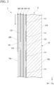
- FIG. 3 is an enlarged view of a region A shown in FIG. 2 .
- the antenna module 1 includes a first substrate 10, a second substrate 20, and a heat dissipation structure 30.
- the heat dissipation structure 30 is formed from, for example, a metal material such as aluminum or stainless steel.
- the first substrate 10 is formed in a rectangular plate shape.
- the first substrate 10 handles a high frequency signal (RF signal) in a millimeter wave band.
- the second substrate 20 is formed in a rectangular plate shape.
- the second substrate 20 handles a baseband signal (BB signal) in a frequency band lower than the high frequency signal.
- the heat dissipation structure 30 is formed in a prismatic shape.
- the heat dissipation structure 30 has a quadrangular prismatic shape, and the first substrate 10 is attached to at least two surfaces (in the present embodiment, all four surfaces) of polygonal side surfaces 30a of the heat dissipation structure 30.
- the second substrate 20 is attached to a first bottom surface 30b perpendicular to the side surfaces 30a of the heat dissipation structure 30.
- the heat dissipation structure 30 is not limited to a quadrangular prismatic shape and may have triangular or pentagonal or other prismatic shapes.
- Adjacent end portions of the first substrate 10 and the second substrate 20 are electrically connected by a connecting portion 40.
- the connecting portion 40 is, for example, a flexible printed circuit board.
- the connecting portion 40 may also be an L-shaped connector.
- a cooling device 50 is attached to a second bottom surface 30c of the heat dissipation structure 30 opposite the first bottom surface 30b.
- a Z-axis direction is set in a direction in which the first bottom surface 30b and the second bottom surface 30c of the heat dissipation structure 30 face each other.
- the X-axis direction is set in a direction in which two of the four side surfaces 30a of the heat dissipation structure 30 face each other.
- the Y-axis direction is set in a direction in which the remaining two surfaces of the four side surfaces 30a of the heat dissipation structure 30 face each other.
- a side to which the arrow of the XYZ orthogonal axis points is defined as a "+ side,” and the opposite side is defined as a "- side.”
- an RFIC 11 (first IC) is provided on a facing surface 10a (first mounting surface) of the first substrate 10, which faces the heat dissipation structure 30.
- Other electronic components (not shown) are provided at positions on a non-facing surface 10b (a surface opposite the facing surface 10a) of the first substrate 10, which are not in the Fresnel zone of the antenna.
- the Fresnel zone is defined as a region where a path difference is equal to or less than half a wavelength (a region where a phase difference is less than or equal to 180°) when electromagnetic waves propagate from a transmission point to a reception point.
- the RFIC 11 generates a predetermined high frequency signal from, for example, a baseband signal supplied by the second substrate 20.
- the first substrate 10 performs both transmission processing and reception processing of the high frequency signal.
- the first substrate 10 is a multilayer substrate including a plurality of conductor layers, as shown in FIG. 3 .
- the first substrate 10 includes conductor layers that are arranged in the order of a first layer 110, a second layer 120, a third layer 130, and a fourth layer 140 from the outside to the inside (toward the heat dissipation structure 30 side).
- An insulator 200 such as a liquid crystal polymer is provided between the first layer 110, the second layer 120, the third layer 130, and the fourth layer 140.
- the first layer 110 is a first antenna layer, and a plurality of first antenna elements 111 (non-feeding elements) are formed.
- the first antenna element 111 is disposed in an array on a non-facing surface 10b side of the first substrate 10.
- the second layer 120 is a second antenna layer, and is formed with a second antenna element 121 (feeding element) disposed on a +X side of the first antenna element 111.
- the first antenna element 111 and the second antenna element 121 function as antennas.
- the third layer 130 forms a ground layer 131 that is electrically grounded.
- An opening portion 132 is formed in the ground layer 131.
- the fourth layer 140 is a signal layer, and is formed with a feed line 141 electrically connected to the RFIC 11.
- the feed line 141 is electromagnetically coupled (for example, capacitively coupled) to the second antenna element 121 via the opening portion 132 of the third layer 130.
- the first substrate 10 can radiate the high frequency signal supplied from the feed line 141 through the first antenna element 111 and the second antenna element 121, or can output the high frequency signal received by the first antenna element 111 and the second antenna element 121 to the feed line 141.
- the form of the antenna is not limited to this configuration, and may also be a form in which the feed line 141 and the second antenna element 121 are electrically and physically connected to each other, or a form in which the first antenna element 111 (non-feeding element) is not provided.
- the feed line 141 is disposed on the facing surface 10a side (+X side) with respect to the ground layer 131.
- the feed line 141 of the present embodiment is exposed on the facing surface 10a of the first substrate 10.
- the first layer 110 (first antenna element 111) is covered with a protective film 210.
- the protective film 210 may be a low-loss dielectric that does not adversely affect the transmission or reception of the high frequency signal.
- the protective film 210 may have a function of improving the gain of the high frequency signal.
- a BBIC 21 (second IC) is provided on a facing surface 20a (second mounting surface) of the second substrate 20, which faces the heat dissipation structure 30.
- other electronic components (not shown) are provided on a non-facing surface 20b (a surface opposite the facing surface 20a) of the second substrate 20.
- Each of four sides of an outer edge of the second substrate 20 is connected to one side of each of the four first substrates 10 adjacent to the second substrate 20, via the connecting portion 40. That is, the baseband signal generated on the second substrate 20 is transmitted to the four first substrates 10 via the connecting portion 40.
- An angle ⁇ between the facing surface 10a of the first substrate 10 and the facing surface 20a of the second substrate 20 is a right angle (90 degrees). According to this configuration, the module size of the antenna module 1 in a planar direction (X-Y plane direction) can be reduced.
- the angle ⁇ between the facing surface 10a of the first substrate 10 and the facing surface 20a of the second substrate 20 may be an acute angle (an angle greater than 0 degrees and less than 90 degrees). Even in this case, the module size of the antenna module 1 in the planar direction (X-Y plane direction) can be reduced.
- the heat dissipation structure 30 includes a support column 31 on a side surface 30a to which the first substrate 10 is attached.
- a pedestal portion 32 is further formed on the side surface 30a.
- the pedestal portion 32 is provided to protrude from the side surface 30a toward the RFIC 11 and is in contact with the RFIC 11 via the heat dissipation sheet 33.
- the heat generated in the RFIC 11 is transferred to the heat dissipation structure 30 (pedestal portion 32) via a heat dissipation sheet 33.
- the support column 31 surround the four sides of the RFIC 11. This can prevent unnecessary radio waves from being emitted externally and make it difficult to access and modify the RFIC 11.
- the heat dissipation structure 30 includes a support column 31 on a first bottom surface 30b, to which the second substrate 20 is attached.
- the pedestal portion 32 is also formed on the first bottom surface 30b.
- the pedestal portion 32 is provided to protrude from the first bottom surface 30b toward the BBIC 21 and is in contact with the BBIC 21 via the heat dissipation sheet 33.
- the heat generated in the BBIC 21 is transferred to the heat dissipation structure 30 (pedestal portion 32) via the heat dissipation sheet 33.
- the support column 31 surround the four sides of the BBIC 21. This can prevent unnecessary radio waves from being emitted externally and make it difficult to access and modify the BBIC 21.
- the heat dissipation structure 30 has a hollow portion 34 with an open second bottom surface 30c opposite the first bottom surface 30b.
- a plurality of heat dissipation plates 35 are provided in the hollow portion 34.
- the cooling device 50 is, for example, a blower that takes in outside air, sends the air to the hollow portion 34, and releases the warm air, which has been heat-exchanged with the heat dissipation plate 35, to the outside.
- the antenna module 1 includes the first substrate 10 that includes the antenna and the feed line 141 and that handles the high frequency signal in the millimeter wave band, the second substrate 20 that handles the baseband signal in the frequency band lower than the high frequency signal, and the heat dissipation structure 30 to which the first substrate 10 and the second substrate 20 are attached.
- the RFIC 11 (first IC) is thermally in contact with the heat dissipation structure 30 and processes the high frequency signal, and is provided on the facing surface 10a (first mounting surface) of the first substrate 10 facing the heat dissipation structure 30.
- the BBIC 21 (second IC) is thermally in contact with the heat dissipation structure 30 and processes the baseband signal, and is provided on the facing surface 20a (second mounting surface) of the second substrate 20 facing the heat dissipation structure 30.
- the connecting portion 40 that electrically connects the adjacent end portions of the first substrate 10 and the second substrate 20 is provided.
- the angle ⁇ between the facing surface 10a and the facing surface 20a is a right angle or an acute angle.
- the RFIC 11 that processes the high frequency signal and the BBIC 21 that processes the baseband signal are thermally brought into contact with the heat dissipation structure 30, allowing the RFIC 11 and the BBIC 21 to be efficiently cooled.
- the first substrate 10 and the second substrate 20 are disposed at a right angle or an acute angle with respect to the heat dissipation structure 30, a smaller module size in the planar direction, and a wider angle of the antenna are possible.
- the connecting portion 40 can be shortened. Therefore, the signal transmission loss is reduced, making susceptibility to disturbance noise or the like difficult.
- the connecting portion 40 includes a flexible printed circuit board. According to this configuration, the electrical connection between the first substrate 10 and the second substrate 20 is easier compared to using an L-shaped connector.
- the heat dissipation structure 30 has a prismatic shape.
- the first substrate 10 is attached to at least two surfaces of the polygonal side surface 30a of the heat dissipation structure 30, and the second substrate 20 is attached to the first bottom surface 30b of the heat dissipation structure 30 perpendicular to the side surface 30a.
- the plurality of first substrates 10 face a plurality of directions (different direction)
- a wider antenna angle is possible.
- 360 degrees can be covered without any gaps.
- the cooling device 50 is attached to the second bottom surface 30c of the heat dissipation structure 30 opposite the first bottom surface 30b. According to this configuration, the cooling device 50 can be disposed without increasing the module size in the planar direction.
- the ground layer 131 is provided in the inner layer of the first substrate 10, and the feed line 141 is disposed on the facing surface 10a side with respect to the ground layer 131. According to this configuration, since the facing surface 10a side is close to the heat dissipation structure 30, the heat dissipation structure 30 functions as an electromagnetic shield for the feed line 141.
- FIG. 4 is a cross-sectional configuration diagram of an antenna module 1A according to the second embodiment.
- the antenna module 1A according to the second embodiment differs from the above-described embodiment in that the cooling device 50A includes a heat pipe 51.
- the heat pipe 51 passes through the interior of the heat dissipation structure 30 and extends to the vicinity of each pedestal portion 32. According to this configuration, the heat obtained at each pedestal portion 32 can be transported to the outside of the heat dissipation structure 30 by the heat pipe 51.
- the cooling device 50A is made of heat dissipation fins, cooling metals, or the like, which are disposed away from the heat dissipation structure 30. As a result, since it is not necessary to provide the heat dissipation plate 35 (see FIG. 2 ) in the hollow portion 34 of the heat dissipation structure 30, the heat dissipation structure 30 can be downsized.
- the cooling device 50 shown in FIG. 2 there may be cases where forced air cooling cannot be performed due to fan failure, dust adhesion, and the like. However, the heat pipe 51 is less susceptible to such failures because the latent heat of the heat medium is utilized.
- FIG. 5 is a cross-sectional configuration diagram of an antenna module 1B according to the third embodiment.
- the antenna module 1B according to the third embodiment differs from the above-described embodiments in that a metal case 60 attached to the heat dissipation structure 30 is provided.
- the metal case 60 includes a bottom wall portion 61 and a peripheral wall portion 62.
- the bottom wall portion 61 has a flat plate shape.
- the peripheral wall portion 62 has a frame shape along an outer peripheral edge of the bottom wall portion 61. That is, the metal case 60 is formed in a bottomed cylindrical shape.
- the first substrate 10 is attached to the heat dissipation structure 30 via a first metal case 60A that surrounds at least part of the facing surface 10a.
- the first metal case 60A surrounds at least the RFIC 11. According to this configuration, the first metal case 60A functions as an electromagnetic shield, thereby suppressing unnecessary radiation caused by a source signal from the RFIC 11.
- the second substrate 20 is attached to the heat dissipation structure 30 via a second metal case 60B that surrounds at least part of the facing surface 20a.
- the second metal case 60B surrounds at least the BBIC 21.
- the second metal case 60B functions as an electromagnetic shield, thereby suppressing unnecessary radiation from a source signal of the BBIC 21.
- FIG. 6 is a cross-sectional configuration diagram of an antenna module 1C according to the fourth embodiment.
- FIG. 7 is an enlarged view of a region B shown in FIG. 6 .
- the antenna module 1C according to the fourth embodiment differs from the above-described embodiments in that a cable 70 is provided that passes through the hollow portion 34 of the heat dissipation structure 30 and is connected to the second substrate 20.
- the BBIC 21 is connected to, for example, an external device (not shown) via the cable 70 and generates a predetermined baseband signal on the basis of a command from the external device. According to this configuration, since the cable 70 is disposed inside the heat dissipation structure 30, it is possible to create a structure in which the cable 70 does not interfere with the transmission or reception of the radio waves of the antenna.
- At least part of a functional component 12 exposed on the non-facing surface 10b of the first substrate 10 is resin-sealed by a first resin sealing member 80.
- at least part of a functional component 22 exposed on the non-facing surface 20b of the second substrate 20 is resin-sealed by the second resin sealing member 90.
- a ground layer 131 is provided in the inner layer of the first substrate 10, and the feed line 141 is disposed on the facing surface 10a side (+X side) of the ground layer 131.
- the feed line 141 is enclosed by the first metal case 60A.
- the leaked radio waves and radio waves from the antenna may interfere with each other, adversely affecting the radiation characteristics (radiation pattern).
- the leaked radio waves from the feed line 141 can be electromagnetically shielded from escaping to the outside of the module.
Landscapes
- Physics & Mathematics (AREA)
- Electromagnetism (AREA)
- Engineering & Computer Science (AREA)
- Microelectronics & Electronic Packaging (AREA)
- Variable-Direction Aerials And Aerial Arrays (AREA)
- Waveguide Aerials (AREA)
Abstract
An antenna module includes a first substrate, a second substrate, and a heat dissipation structure. An RFIC (first IC) is provided on a facing surface (first mounting surface) of the first substrate facing the heat dissipation structure. The RFIC is thermally in contact with the heat dissipation structure and processes a high frequency signal. ABBIC (second IC) is provided to be thermally in contact with the heat dissipation structure and to process a baseband signal on a facing surface (second mounting surface) of the second substrate facing the heat dissipation structure. A connecting portion which electrically connects adjacent end portions of the first substrate and the second substrate, is provided. An angle θ between the facing surfaces is a right angle or an acute angle.
Description
- Priority is claimed on
Japanese Patent Application No. 2023-194444, filed November 15, 2023 - The present invention pertains to an antenna module.
-
Japanese Unexamined Patent Application, First Publication No. 2020-123946 - Since the antenna module includes a trapezoidal substrate portion, a wider antenna angle is possible. However, there is a problem in that the module size in a planar direction of the antenna module is increased.
- In addition, the antenna module does not consider a heat dissipation structure for the integrated circuit (IC) provided on the back surface of the substrate portion.
- The present invention has been made in view of the above-described problems, and an object of the present invention is to provide an antenna module including a heat dissipation structure for an IC and allowing a smaller module size in a planar direction and a wider angle of an antenna.
- A first aspect of the present invention relates to an antenna module including a first substrate that includes an antenna and a feed line and that handles a high frequency signal in a millimeter wave band; a second substrate that handles a baseband signal in a frequency band lower than the frequency band of the high frequency signal; and a heat dissipation structure to which the first substrate and the second substrate are attached, wherein a first IC that is thermally in contact with the heat dissipation structure and that processes the high frequency signal is provided on a first mounting surface of the first substrate facing the heat dissipation structure, a second IC that is thermally in contact with the heat dissipation structure and that processes the baseband signal is provided on a second mounting surface of the second substrate facing the heat dissipation structure, a connecting portion that electrically connects adjacent end portions of the first substrate and the second substrate is provided, and an angle between the first mounting surface and the second mounting surface is a right angle or an acute angle.
- According to the first aspect of the present invention, the first IC that processes the high frequency signal and the second IC that processes the baseband signal are thermally brought into contact with the heat dissipation structure, allowing the first IC and the second IC to be efficiently cooled. In addition, by disposing the first substrate and the second substrate with respect to the heat dissipation structure at a right angle or an acute angle, a smaller module size in the planar direction and a wider antenna angle are possible. In addition, by electrically connecting the adjacent end portions of the first substrate and the second substrate, the connecting portion can be shortened. Therefore, the signal transmission loss is reduced, making susceptibility to disturbance noise or the like difficult.
- A second aspect of the present invention relates to the antenna module according to the first aspect, in which the connecting portion may include a flexible printed circuit board.
- A third aspect of the present invention relates to the antenna module according to the first or second aspect, in which the heat dissipation structure may have a prismatic shape, the first substrate may be attached to at least two surfaces of polygonal side surfaces of the heat dissipation structure, and the second substrate may be attached to a first bottom surface of the heat dissipation structure perpendicular to the side surfaces.
- A fourth aspect of the present invention relates to the antenna module according to the third aspect, in which a cooling device may be attached to the second bottom surface of the heat dissipation structure opposite the first bottom surface.
- A fifth aspect of the present invention relates to the antenna module according to the third or fourth aspect, in which the heat dissipation structure may include a hollow portion with an open second bottom surface opposite the first bottom surface, and may include a cable that passes through the hollow portion and is connected to the second substrate.
- A sixth aspect of the present invention is the antenna module according to any one of the first to fifth aspects, in which a ground layer may be provided in an inner layer of the first substrate, and the feed line may be disposed on a first mounting surface side with respect to the ground layer.
- A seventh aspect of the present invention is the antenna module according to any one of the first to sixth aspects, in which the first substrate may be attached to the heat dissipation structure via a first metal case that surrounds at least part of the first mounting surface, and the second substrate may be attached to the heat dissipation structure via a second metal case that surrounds at least part of the second mounting surface.
- An eighth aspect of the present invention relates to the antenna module according to the seventh aspect, wherein the first metal case may surround at least the first IC.
- A ninth aspect of the present invention is the antenna module according to the seventh or eighth aspect, in which the second metal case may surround at least the second IC.
- A tenth aspect of the present invention is the antenna module according to any one of the seventh to ninth aspects, in which a ground layer may be provided in an inner layer of the first substrate, the feed line may be disposed on a first mounting surface side with respect to the ground layer, and the feed line may be surrounded by the first metal case.
- An eleventh aspect of the present invention may further the antenna module according to any one of the first to tenth aspects, further including a first resin sealing member that resin-seals at least part of a functional component exposed on a surface of the first substrate opposite the first mounting surface; and a second resin sealing member that resin-seals at least part of a functional component exposed on a surface of the second substrate opposite the second mounting surface.
- According to one aspect of the present invention, a heat dissipation structure for an IC is provided, making a smaller module size in the planar direction and a wider antenna angle possible.
-
-
FIG. 1 is a schematic perspective view of an antenna module according to a first embodiment. -
FIG. 2 is a cross-sectional configuration diagram of the antenna module according to the first embodiment. -
FIG. 3 is an enlarged view of a region A shown inFIG. 2 . -
FIG. 4 is a cross-sectional configuration diagram of an antenna module according to a second embodiment. -
FIG. 5 is a cross-sectional configuration diagram of an antenna module according to a third embodiment. -
FIG. 6 is a cross-sectional configuration diagram of an antenna module according to a fourth embodiment. -
FIG. 7 is an enlarged view of a region B shown inFIG. 6 . - Hereinafter, an antenna module according to each embodiment of the present invention will be described with reference to the accompanying drawings.
-
FIG. 1 is a schematic perspective view of anantenna module 1 according to a first embodiment.FIG. 2 is a cross-sectional configuration diagram of theantenna module 1 according to the first embodiment.FIG. 3 is an enlarged view of a region A shown inFIG. 2 . - As shown in
FIG. 1 , theantenna module 1 according to the present embodiment includes afirst substrate 10, asecond substrate 20, and aheat dissipation structure 30. Theheat dissipation structure 30 is formed from, for example, a metal material such as aluminum or stainless steel. - The
first substrate 10 is formed in a rectangular plate shape. Thefirst substrate 10 handles a high frequency signal (RF signal) in a millimeter wave band. In addition, thesecond substrate 20 is formed in a rectangular plate shape. Thesecond substrate 20 handles a baseband signal (BB signal) in a frequency band lower than the high frequency signal. Theheat dissipation structure 30 is formed in a prismatic shape. - The
heat dissipation structure 30 according to the present embodiment has a quadrangular prismatic shape, and thefirst substrate 10 is attached to at least two surfaces (in the present embodiment, all four surfaces) ofpolygonal side surfaces 30a of theheat dissipation structure 30. Thesecond substrate 20 is attached to afirst bottom surface 30b perpendicular to theside surfaces 30a of theheat dissipation structure 30. Theheat dissipation structure 30 is not limited to a quadrangular prismatic shape and may have triangular or pentagonal or other prismatic shapes. - Adjacent end portions of the
first substrate 10 and thesecond substrate 20 are electrically connected by a connectingportion 40. The connectingportion 40 is, for example, a flexible printed circuit board. The connectingportion 40 may also be an L-shaped connector. Acooling device 50 is attached to asecond bottom surface 30c of theheat dissipation structure 30 opposite thefirst bottom surface 30b. - In addition, in the following description, the XYZ Cartesian coordinate system may be set, and a positional relationship of respective members may be described with reference to the XYZ Cartesian coordinate system. As shown in
FIG. 1 , a Z-axis direction is set in a direction in which thefirst bottom surface 30b and thesecond bottom surface 30c of theheat dissipation structure 30 face each other. The X-axis direction is set in a direction in which two of the fourside surfaces 30a of theheat dissipation structure 30 face each other. The Y-axis direction is set in a direction in which the remaining two surfaces of the fourside surfaces 30a of theheat dissipation structure 30 face each other. In addition, a side to which the arrow of the XYZ orthogonal axis points is defined as a "+ side," and the opposite side is defined as a "- side." - As shown in
FIG. 2 , an RFIC 11 (first IC) is provided on a facingsurface 10a (first mounting surface) of thefirst substrate 10, which faces theheat dissipation structure 30. Other electronic components (not shown) are provided at positions on anon-facing surface 10b (a surface opposite the facingsurface 10a) of thefirst substrate 10, which are not in the Fresnel zone of the antenna. The Fresnel zone is defined as a region where a path difference is equal to or less than half a wavelength (a region where a phase difference is less than or equal to 180°) when electromagnetic waves propagate from a transmission point to a reception point. TheRFIC 11 generates a predetermined high frequency signal from, for example, a baseband signal supplied by thesecond substrate 20. Thefirst substrate 10 performs both transmission processing and reception processing of the high frequency signal. - The
first substrate 10 is a multilayer substrate including a plurality of conductor layers, as shown inFIG. 3 . Specifically, thefirst substrate 10 includes conductor layers that are arranged in the order of afirst layer 110, asecond layer 120, athird layer 130, and afourth layer 140 from the outside to the inside (toward theheat dissipation structure 30 side). Aninsulator 200 such as a liquid crystal polymer is provided between thefirst layer 110, thesecond layer 120, thethird layer 130, and thefourth layer 140. - The
first layer 110 is a first antenna layer, and a plurality of first antenna elements 111 (non-feeding elements) are formed. Thefirst antenna element 111 is disposed in an array on anon-facing surface 10b side of thefirst substrate 10. Thesecond layer 120 is a second antenna layer, and is formed with a second antenna element 121 (feeding element) disposed on a +X side of thefirst antenna element 111. Thefirst antenna element 111 and thesecond antenna element 121 function as antennas. - The
third layer 130 forms aground layer 131 that is electrically grounded. Anopening portion 132 is formed in theground layer 131. Thefourth layer 140 is a signal layer, and is formed with afeed line 141 electrically connected to theRFIC 11. Thefeed line 141 is electromagnetically coupled (for example, capacitively coupled) to thesecond antenna element 121 via theopening portion 132 of thethird layer 130. By this coupling, thefirst substrate 10 can radiate the high frequency signal supplied from thefeed line 141 through thefirst antenna element 111 and thesecond antenna element 121, or can output the high frequency signal received by thefirst antenna element 111 and thesecond antenna element 121 to thefeed line 141. - The form of the antenna is not limited to this configuration, and may also be a form in which the
feed line 141 and thesecond antenna element 121 are electrically and physically connected to each other, or a form in which the first antenna element 111 (non-feeding element) is not provided. - The
feed line 141 is disposed on the facingsurface 10a side (+X side) with respect to theground layer 131. Thefeed line 141 of the present embodiment is exposed on the facingsurface 10a of thefirst substrate 10. The first layer 110 (first antenna element 111) is covered with aprotective film 210. Theprotective film 210 may be a low-loss dielectric that does not adversely affect the transmission or reception of the high frequency signal. In addition, theprotective film 210 may have a function of improving the gain of the high frequency signal. - Returning to
FIG. 2 , a BBIC 21 (second IC) is provided on a facingsurface 20a (second mounting surface) of thesecond substrate 20, which faces theheat dissipation structure 30. In addition, other electronic components (not shown) are provided on anon-facing surface 20b (a surface opposite the facingsurface 20a) of thesecond substrate 20. Each of four sides of an outer edge of thesecond substrate 20 is connected to one side of each of the fourfirst substrates 10 adjacent to thesecond substrate 20, via the connectingportion 40. That is, the baseband signal generated on thesecond substrate 20 is transmitted to the fourfirst substrates 10 via the connectingportion 40. - An angle θ between the facing
surface 10a of thefirst substrate 10 and the facingsurface 20a of thesecond substrate 20 is a right angle (90 degrees). According to this configuration, the module size of theantenna module 1 in a planar direction (X-Y plane direction) can be reduced. The angle θ between the facingsurface 10a of thefirst substrate 10 and the facingsurface 20a of thesecond substrate 20 may be an acute angle (an angle greater than 0 degrees and less than 90 degrees). Even in this case, the module size of theantenna module 1 in the planar direction (X-Y plane direction) can be reduced. - The
heat dissipation structure 30 includes asupport column 31 on aside surface 30a to which thefirst substrate 10 is attached. Apedestal portion 32 is further formed on theside surface 30a. Thepedestal portion 32 is provided to protrude from theside surface 30a toward theRFIC 11 and is in contact with theRFIC 11 via theheat dissipation sheet 33. As a result, the heat generated in theRFIC 11 is transferred to the heat dissipation structure 30 (pedestal portion 32) via aheat dissipation sheet 33. It is preferable that thesupport column 31 surround the four sides of theRFIC 11. This can prevent unnecessary radio waves from being emitted externally and make it difficult to access and modify theRFIC 11. - In addition, the
heat dissipation structure 30 includes asupport column 31 on a firstbottom surface 30b, to which thesecond substrate 20 is attached. Thepedestal portion 32 is also formed on the firstbottom surface 30b. Thepedestal portion 32 is provided to protrude from the firstbottom surface 30b toward theBBIC 21 and is in contact with theBBIC 21 via theheat dissipation sheet 33. As a result, the heat generated in theBBIC 21 is transferred to the heat dissipation structure 30 (pedestal portion 32) via theheat dissipation sheet 33. It is preferable that thesupport column 31 surround the four sides of theBBIC 21. This can prevent unnecessary radio waves from being emitted externally and make it difficult to access and modify theBBIC 21. - The
heat dissipation structure 30 has ahollow portion 34 with an open secondbottom surface 30c opposite the firstbottom surface 30b. A plurality ofheat dissipation plates 35 are provided in thehollow portion 34. Thecooling device 50 is, for example, a blower that takes in outside air, sends the air to thehollow portion 34, and releases the warm air, which has been heat-exchanged with theheat dissipation plate 35, to the outside. - As described above, the
antenna module 1 according to the present embodiment includes thefirst substrate 10 that includes the antenna and thefeed line 141 and that handles the high frequency signal in the millimeter wave band, thesecond substrate 20 that handles the baseband signal in the frequency band lower than the high frequency signal, and theheat dissipation structure 30 to which thefirst substrate 10 and thesecond substrate 20 are attached. The RFIC 11 (first IC) is thermally in contact with theheat dissipation structure 30 and processes the high frequency signal, and is provided on the facingsurface 10a (first mounting surface) of thefirst substrate 10 facing theheat dissipation structure 30. The BBIC 21 (second IC) is thermally in contact with theheat dissipation structure 30 and processes the baseband signal, and is provided on the facingsurface 20a (second mounting surface) of thesecond substrate 20 facing theheat dissipation structure 30. The connectingportion 40 that electrically connects the adjacent end portions of thefirst substrate 10 and thesecond substrate 20 is provided. The angle θ between the facingsurface 10a and the facingsurface 20a is a right angle or an acute angle. - According to this configuration, the
RFIC 11 that processes the high frequency signal and theBBIC 21 that processes the baseband signal are thermally brought into contact with theheat dissipation structure 30, allowing theRFIC 11 and theBBIC 21 to be efficiently cooled. In addition, by disposing thefirst substrate 10 and thesecond substrate 20 at a right angle or an acute angle with respect to theheat dissipation structure 30, a smaller module size in the planar direction, and a wider angle of the antenna are possible. In addition, by electrically connecting the adjacent end portions of thefirst substrate 10 and thesecond substrate 20, the connectingportion 40 can be shortened. Therefore, the signal transmission loss is reduced, making susceptibility to disturbance noise or the like difficult. - In addition, in the present embodiment, the connecting
portion 40 includes a flexible printed circuit board. According to this configuration, the electrical connection between thefirst substrate 10 and thesecond substrate 20 is easier compared to using an L-shaped connector. - In addition, in the present embodiment, the
heat dissipation structure 30 has a prismatic shape. Thefirst substrate 10 is attached to at least two surfaces of thepolygonal side surface 30a of theheat dissipation structure 30, and thesecond substrate 20 is attached to the firstbottom surface 30b of theheat dissipation structure 30 perpendicular to theside surface 30a. According to this configuration, since the plurality offirst substrates 10 face a plurality of directions (different direction), a wider antenna angle is possible. For example, in a case where the beam directions from the fourfirst substrates 10 are ±45 degrees as in the present embodiment, 360 degrees can be covered without any gaps. - In addition, in the present embodiment, the
cooling device 50 is attached to thesecond bottom surface 30c of theheat dissipation structure 30 opposite the firstbottom surface 30b. According to this configuration, thecooling device 50 can be disposed without increasing the module size in the planar direction. - In addition, in the present embodiment, the
ground layer 131 is provided in the inner layer of thefirst substrate 10, and thefeed line 141 is disposed on the facingsurface 10a side with respect to theground layer 131. According to this configuration, since the facingsurface 10a side is close to theheat dissipation structure 30, theheat dissipation structure 30 functions as an electromagnetic shield for thefeed line 141. - A second embodiment of the present invention will be described below. In the following description, the same or equivalent components as those in the above-described embodiment are designated by the same reference numerals, and the description thereof will be simplified or omitted.
-
FIG. 4 is a cross-sectional configuration diagram of anantenna module 1A according to the second embodiment. - As shown in
FIG. 4 , theantenna module 1A according to the second embodiment differs from the above-described embodiment in that thecooling device 50A includes aheat pipe 51. - The
heat pipe 51 passes through the interior of theheat dissipation structure 30 and extends to the vicinity of eachpedestal portion 32. According to this configuration, the heat obtained at eachpedestal portion 32 can be transported to the outside of theheat dissipation structure 30 by theheat pipe 51. Specifically, thecooling device 50A is made of heat dissipation fins, cooling metals, or the like, which are disposed away from theheat dissipation structure 30. As a result, since it is not necessary to provide the heat dissipation plate 35 (seeFIG. 2 ) in thehollow portion 34 of theheat dissipation structure 30, theheat dissipation structure 30 can be downsized. In addition, in thecooling device 50 shown inFIG. 2 , there may be cases where forced air cooling cannot be performed due to fan failure, dust adhesion, and the like. However, theheat pipe 51 is less susceptible to such failures because the latent heat of the heat medium is utilized. - A third embodiment of the present invention will be described below. In the following description, the same or equivalent components as those in the above-described embodiment are designated by the same reference numerals, and the description thereof will be simplified or omitted.
-
FIG. 5 is a cross-sectional configuration diagram of anantenna module 1B according to the third embodiment. - As shown in
FIG. 5 , theantenna module 1B according to the third embodiment differs from the above-described embodiments in that ametal case 60 attached to theheat dissipation structure 30 is provided. - The
metal case 60 includes abottom wall portion 61 and aperipheral wall portion 62. Thebottom wall portion 61 has a flat plate shape. Theperipheral wall portion 62 has a frame shape along an outer peripheral edge of thebottom wall portion 61. That is, themetal case 60 is formed in a bottomed cylindrical shape. - The
first substrate 10 is attached to theheat dissipation structure 30 via afirst metal case 60A that surrounds at least part of the facingsurface 10a. Thefirst metal case 60A surrounds at least theRFIC 11. According to this configuration, thefirst metal case 60A functions as an electromagnetic shield, thereby suppressing unnecessary radiation caused by a source signal from theRFIC 11. - In addition, the
second substrate 20 is attached to theheat dissipation structure 30 via asecond metal case 60B that surrounds at least part of the facingsurface 20a. Thesecond metal case 60B surrounds at least theBBIC 21. According to this configuration, thesecond metal case 60B functions as an electromagnetic shield, thereby suppressing unnecessary radiation from a source signal of theBBIC 21. - A fourth embodiment of the present invention will be described below. In the following description, the same or equivalent components as those in the above-described embodiment are designated by the same reference numerals, and the description thereof will be simplified or omitted.
-
FIG. 6 is a cross-sectional configuration diagram of anantenna module 1C according to the fourth embodiment.FIG. 7 is an enlarged view of a region B shown inFIG. 6 . - As shown in
FIG. 6 , theantenna module 1C according to the fourth embodiment differs from the above-described embodiments in that acable 70 is provided that passes through thehollow portion 34 of theheat dissipation structure 30 and is connected to thesecond substrate 20. - The
BBIC 21 is connected to, for example, an external device (not shown) via thecable 70 and generates a predetermined baseband signal on the basis of a command from the external device. According to this configuration, since thecable 70 is disposed inside theheat dissipation structure 30, it is possible to create a structure in which thecable 70 does not interfere with the transmission or reception of the radio waves of the antenna. - In addition, in the fourth embodiment, at least part of a
functional component 12 exposed on thenon-facing surface 10b of thefirst substrate 10 is resin-sealed by a firstresin sealing member 80. Similarly, at least part of afunctional component 22 exposed on thenon-facing surface 20b of thesecond substrate 20 is resin-sealed by the secondresin sealing member 90. According to this configuration, it is possible to prevent damage, falling-off, or modification by resin-sealing thefunctional components - In addition, as shown in
FIG. 7 , aground layer 131 is provided in the inner layer of thefirst substrate 10, and thefeed line 141 is disposed on the facingsurface 10a side (+X side) of theground layer 131. Thefeed line 141 is enclosed by thefirst metal case 60A. In a case where a signal leaking from the feed line 141 (signal line) is radiated to the outside, the leaked radio waves and radio waves from the antenna may interfere with each other, adversely affecting the radiation characteristics (radiation pattern). According to the above configuration, the leaked radio waves from thefeed line 141 can be electromagnetically shielded from escaping to the outside of the module. - Although preferred embodiments of the present invention have been described and explained above, it should be understood that these embodiments are exemplary and should not be considered as limiting. Additions, omissions, substitutions, and other modifications can be made without departing from the scope of the present invention. Therefore, the present invention should not be considered as being limited by the aforementioned description but is only limited by the claims.
- In addition, it is possible to appropriately replace the constituent elements in the above-described embodiments with well-known constituent elements without departing from the spirit of the present invention, and the above-described embodiments and modification examples may be appropriately combined.
Claims (11)
- An antenna module comprising:a first substrate that includes an antenna and a feed line and that handles a high frequency signal in a millimeter wave band;a second substrate that handles a baseband signal in a frequency band lower than the frequency band of the high frequency signal; anda heat dissipation structure to which the first substrate and the second substrate are attached,wherein a first IC that is thermally in contact with the heat dissipation structure and that processes the high frequency signal is provided on a first mounting surface of the first substrate facing the heat dissipation structure,a second IC that is thermally in contact with the heat dissipation structure and that processes the baseband signal is provided on a second mounting surface of the second substrate facing the heat dissipation structure,a connecting portion that electrically connects adjacent end portions of the first substrate and the second substrate is provided, andan angle between the first mounting surface and the second mounting surface is a right angle or an acute angle.
- The antenna module according to Claim 1,
wherein the connecting portion includes a flexible printed circuit board. - The antenna module according to Claim 1 or 2,wherein the heat dissipation structure has a prismatic shape,the first substrate is attached to at least two surfaces of polygonal side surfaces of the heat dissipation structure, andthe second substrate is attached to a first bottom surface of the heat dissipation structure perpendicular to the side surfaces.
- The antenna module according to Claim 3,
wherein a cooling device is attached to a second bottom surface of the heat dissipation structure opposite the first bottom surface. - The antenna module according to Claim 3 or 4,wherein the heat dissipation structure includes a hollow portion with an open second bottom surface opposite the first bottom surface, andthe antenna module includes a cable that passes through the hollow portion and is connected to the second substrate.
- The antenna module according to any one of the preceding claims,wherein a ground layer is provided in an inner layer of the first substrate, andthe feed line is disposed on a first mounting surface side with respect to the ground layer.
- The antenna module according to any one of the preceding claims,wherein the first substrate is attached to the heat dissipation structure via a first metal case that surrounds at least part of the first mounting surface, andthe second substrate is attached to the heat dissipation structure via a second metal case that surrounds at least part of the second mounting surface.
- The antenna module according to Claim 7,
wherein the first metal case surrounds at least the first IC. - The antenna module according to Claim 7 or 8,
wherein the second metal case surrounds at least the second IC. - The antenna module according to any one of the claims 7 to 9,wherein a ground layer is provided in an inner layer of the first substrate,the feed line is disposed on a first mounting surface side with respect to the ground layer, andthe feed line is surrounded by the first metal case.
- The antenna module according to any one of the preceding claims, further comprising:a first resin sealing member that resin-seals at least part of a functional component exposed on a surface of the first substrate opposite the first mounting surface; anda second resin sealing member that resin-seals at least part of a functional component exposed on a surface of the second substrate opposite the second mounting surface.
Applications Claiming Priority (1)
| Application Number | Priority Date | Filing Date | Title |
|---|---|---|---|
| JP2023194444A JP2025080989A (en) | 2023-11-15 | 2023-11-15 | Antenna Module |
Publications (1)
| Publication Number | Publication Date |
|---|---|
| EP4557506A1 true EP4557506A1 (en) | 2025-05-21 |
Family
ID=93291884
Family Applications (1)
| Application Number | Title | Priority Date | Filing Date |
|---|---|---|---|
| EP24208909.2A Pending EP4557506A1 (en) | 2023-11-15 | 2024-10-25 | Antenna module |
Country Status (3)
| Country | Link |
|---|---|
| US (1) | US20250158295A1 (en) |
| EP (1) | EP4557506A1 (en) |
| JP (1) | JP2025080989A (en) |
Citations (5)
| Publication number | Priority date | Publication date | Assignee | Title |
|---|---|---|---|---|
| US20200243957A1 (en) * | 2019-01-30 | 2020-07-30 | Murata Manufacturing Co., Ltd. | Antenna module and antenna device |
| US20200329549A1 (en) * | 2019-04-15 | 2020-10-15 | Samsung Electronics Co, Ltd. | Electronic device including antenna and heat dissipation structure |
| CN112201948A (en) * | 2019-07-08 | 2021-01-08 | 深圳市大富科技股份有限公司 | Active antenna unit, shell and inner shell |
| US20210410268A1 (en) * | 2018-11-12 | 2021-12-30 | Samsung Electronics Co., Ltd. | Electronic device including heat dissipation structure |
| KR20220080540A (en) * | 2020-12-07 | 2022-06-14 | 주식회사 하우앳 | Millimeter wave transceiver with improved heat dissipation |
Family Cites Families (21)
| Publication number | Priority date | Publication date | Assignee | Title |
|---|---|---|---|---|
| US6891726B1 (en) * | 2003-10-30 | 2005-05-10 | Intel Corporation | Heat sink and antenna |
| EP3069586B1 (en) * | 2013-11-13 | 2017-09-20 | Thomson Licensing | Heatsink alignment to printed circuit board |
| KR102501935B1 (en) * | 2016-08-31 | 2023-02-21 | 삼성전자 주식회사 | Antenna device and electronic device comprising the same |
| FI128822B (en) * | 2017-11-15 | 2020-12-31 | Teknologian Tutkimuskeskus Vtt Oy | Antenna array and method for manufacturing thereof |
| WO2019133195A1 (en) * | 2017-12-29 | 2019-07-04 | Commscope Technologies Llc | Compact phased array millimeter wave communications systems suitable for fixed wireless access applications |
| WO2019176778A1 (en) * | 2018-03-14 | 2019-09-19 | 株式会社村田製作所 | High frequency module and communication device |
| US10912204B2 (en) * | 2018-03-30 | 2021-02-02 | Samsung Electro-Mechanics Co., Ltd. | Electronic device and rigid-flexible substrate module |
| KR102280051B1 (en) * | 2018-08-22 | 2021-07-21 | 삼성전자주식회사 | Antenna module, and electronic device with the same |
| KR102137093B1 (en) * | 2019-08-05 | 2020-07-23 | 삼성전기주식회사 | Antenna module and electronic device including thereof |
| WO2021059671A1 (en) * | 2019-09-27 | 2021-04-01 | 株式会社村田製作所 | Antenna module and communication device provided with same |
| CN114730986B (en) * | 2019-11-15 | 2025-06-03 | 索尼集团公司 | Portable Electronic Devices |
| KR102885259B1 (en) * | 2020-07-31 | 2025-11-14 | 삼성전자주식회사 | Electronic Device comprising Shielding Structure and Heat-Radiating Structure |
| CN215116790U (en) * | 2021-03-04 | 2021-12-10 | 深圳市道通智能汽车有限公司 | A radar and early warning system |
| EP4350756B1 (en) * | 2021-05-26 | 2025-07-23 | Mitsubishi Electric Corporation | Antenna apparatus |
| CN115548668A (en) * | 2021-06-30 | 2022-12-30 | 华为技术有限公司 | Antenna and base station |
| WO2023088446A1 (en) * | 2021-11-21 | 2023-05-25 | 华为技术有限公司 | Antenna and communication system |
| US20230408619A1 (en) * | 2022-05-20 | 2023-12-21 | Anduril Industries, Inc. | Detecting, tracking, and transmitting to identified objects using models in a modular system |
| CN119856342A (en) * | 2022-10-03 | 2025-04-18 | 株式会社村田制作所 | Antenna module and communication device equipped with the same |
| TWI846129B (en) * | 2022-11-02 | 2024-06-21 | 和碩聯合科技股份有限公司 | Antenna module and electronic device |
| JP7309089B1 (en) * | 2023-01-23 | 2023-07-14 | 株式会社フジクラ | wireless module |
| JP7364807B1 (en) * | 2023-01-23 | 2023-10-18 | 株式会社フジクラ | wireless module |
-
2023
- 2023-11-15 JP JP2023194444A patent/JP2025080989A/en active Pending
-
2024
- 2024-10-25 EP EP24208909.2A patent/EP4557506A1/en active Pending
- 2024-10-30 US US18/931,228 patent/US20250158295A1/en active Pending
Patent Citations (6)
| Publication number | Priority date | Publication date | Assignee | Title |
|---|---|---|---|---|
| US20210410268A1 (en) * | 2018-11-12 | 2021-12-30 | Samsung Electronics Co., Ltd. | Electronic device including heat dissipation structure |
| US20200243957A1 (en) * | 2019-01-30 | 2020-07-30 | Murata Manufacturing Co., Ltd. | Antenna module and antenna device |
| JP2020123946A (en) | 2019-01-30 | 2020-08-13 | 株式会社村田製作所 | Antenna module and antenna device |
| US20200329549A1 (en) * | 2019-04-15 | 2020-10-15 | Samsung Electronics Co, Ltd. | Electronic device including antenna and heat dissipation structure |
| CN112201948A (en) * | 2019-07-08 | 2021-01-08 | 深圳市大富科技股份有限公司 | Active antenna unit, shell and inner shell |
| KR20220080540A (en) * | 2020-12-07 | 2022-06-14 | 주식회사 하우앳 | Millimeter wave transceiver with improved heat dissipation |
Also Published As
| Publication number | Publication date |
|---|---|
| JP2025080989A (en) | 2025-05-27 |
| US20250158295A1 (en) | 2025-05-15 |
Similar Documents
| Publication | Publication Date | Title |
|---|---|---|
| US11756902B2 (en) | High-frequency module | |
| EP2919323A1 (en) | Array antenna | |
| US11862866B2 (en) | Antenna module and electronic device | |
| US12218432B2 (en) | Antenna module and communication apparatus equipped with the same | |
| CN118232026B (en) | Antenna structure and electronic equipment | |
| JP2024104143A (en) | Wireless Module | |
| EP4557506A1 (en) | Antenna module | |
| US20210328335A1 (en) | Antenna, array antenna, and wireless communication device | |
| TWI752780B (en) | Antenna structure with wide beamwidth | |
| US12586928B2 (en) | Antenna device and communication device | |
| US20240405417A1 (en) | Radar sensor with recessed radome | |
| CN114006149A (en) | Electronic equipment | |
| EP4554000A1 (en) | Antenna module | |
| US20210307221A1 (en) | Shield structure and electronic device | |
| US10615487B2 (en) | Antenna waveguide and antenna module thereof | |
| WO2018070296A1 (en) | Electronic control unit | |
| CN116888823A (en) | Antenna device | |
| US12592487B2 (en) | Antenna device | |
| CN223911855U (en) | terminal equipment | |
| US12501595B2 (en) | Electronic apparatus and electro-magnetic interference reduction method | |
| JP7819033B2 (en) | Antenna device, antenna built-in device | |
| US20250022816A1 (en) | Radio frequency module and manufacturing method of radio frequency module | |
| US12074360B2 (en) | RFIC assembled antenna | |
| JP7852743B2 (en) | Antenna module and communication device equipped with it | |
| US20230328940A1 (en) | Electronic device |
Legal Events
| Date | Code | Title | Description |
|---|---|---|---|
| PUAI | Public reference made under article 153(3) epc to a published international application that has entered the european phase |
Free format text: ORIGINAL CODE: 0009012 |
|
| STAA | Information on the status of an ep patent application or granted ep patent |
Free format text: STATUS: REQUEST FOR EXAMINATION WAS MADE |
|
| 17P | Request for examination filed |
Effective date: 20241025 |
|
| AK | Designated contracting states |
Kind code of ref document: A1 Designated state(s): AL AT BE BG CH CY CZ DE DK EE ES FI FR GB GR HR HU IE IS IT LI LT LU LV MC ME MK MT NL NO PL PT RO RS SE SI SK SM TR |