EP4557376A1 - Vertical heterojunction bipolar transistor - Google Patents
Vertical heterojunction bipolar transistor Download PDFInfo
- Publication number
- EP4557376A1 EP4557376A1 EP24181005.0A EP24181005A EP4557376A1 EP 4557376 A1 EP4557376 A1 EP 4557376A1 EP 24181005 A EP24181005 A EP 24181005A EP 4557376 A1 EP4557376 A1 EP 4557376A1
- Authority
- EP
- European Patent Office
- Prior art keywords
- collector
- sub
- semiconductor material
- collector region
- region
- Prior art date
- Legal status (The legal status is an assumption and is not a legal conclusion. Google has not performed a legal analysis and makes no representation as to the accuracy of the status listed.)
- Pending
Links
Images
Classifications
-
- H—ELECTRICITY
- H10—SEMICONDUCTOR DEVICES; ELECTRIC SOLID-STATE DEVICES NOT OTHERWISE PROVIDED FOR
- H10D—INORGANIC ELECTRIC SEMICONDUCTOR DEVICES
- H10D10/00—Bipolar junction transistors [BJT]
- H10D10/80—Heterojunction BJTs
- H10D10/821—Vertical heterojunction BJTs
-
- H—ELECTRICITY
- H10—SEMICONDUCTOR DEVICES; ELECTRIC SOLID-STATE DEVICES NOT OTHERWISE PROVIDED FOR
- H10D—INORGANIC ELECTRIC SEMICONDUCTOR DEVICES
- H10D10/00—Bipolar junction transistors [BJT]
- H10D10/01—Manufacture or treatment
- H10D10/021—Manufacture or treatment of heterojunction BJTs [HBT]
-
- H—ELECTRICITY
- H10—SEMICONDUCTOR DEVICES; ELECTRIC SOLID-STATE DEVICES NOT OTHERWISE PROVIDED FOR
- H10D—INORGANIC ELECTRIC SEMICONDUCTOR DEVICES
- H10D10/00—Bipolar junction transistors [BJT]
- H10D10/80—Heterojunction BJTs
- H10D10/821—Vertical heterojunction BJTs
- H10D10/891—Vertical heterojunction BJTs comprising lattice-mismatched active layers, e.g. SiGe strained-layer transistors
-
- H—ELECTRICITY
- H10—SEMICONDUCTOR DEVICES; ELECTRIC SOLID-STATE DEVICES NOT OTHERWISE PROVIDED FOR
- H10D—INORGANIC ELECTRIC SEMICONDUCTOR DEVICES
- H10D62/00—Semiconductor bodies, or regions thereof, of devices having potential barriers
- H10D62/10—Shapes, relative sizes or dispositions of the regions of the semiconductor bodies; Shapes of the semiconductor bodies
- H10D62/13—Semiconductor regions connected to electrodes carrying current to be rectified, amplified or switched, e.g. source or drain regions
- H10D62/133—Emitter regions of BJTs
- H10D62/136—Emitter regions of BJTs of heterojunction BJTs
-
- H—ELECTRICITY
- H10—SEMICONDUCTOR DEVICES; ELECTRIC SOLID-STATE DEVICES NOT OTHERWISE PROVIDED FOR
- H10D—INORGANIC ELECTRIC SEMICONDUCTOR DEVICES
- H10D62/00—Semiconductor bodies, or regions thereof, of devices having potential barriers
- H10D62/10—Shapes, relative sizes or dispositions of the regions of the semiconductor bodies; Shapes of the semiconductor bodies
- H10D62/13—Semiconductor regions connected to electrodes carrying current to be rectified, amplified or switched, e.g. source or drain regions
- H10D62/137—Collector regions of BJTs
-
- H—ELECTRICITY
- H10—SEMICONDUCTOR DEVICES; ELECTRIC SOLID-STATE DEVICES NOT OTHERWISE PROVIDED FOR
- H10D—INORGANIC ELECTRIC SEMICONDUCTOR DEVICES
- H10D62/00—Semiconductor bodies, or regions thereof, of devices having potential barriers
- H10D62/10—Shapes, relative sizes or dispositions of the regions of the semiconductor bodies; Shapes of the semiconductor bodies
- H10D62/13—Semiconductor regions connected to electrodes carrying current to be rectified, amplified or switched, e.g. source or drain regions
- H10D62/137—Collector regions of BJTs
- H10D62/138—Pedestal collectors
-
- H—ELECTRICITY
- H10—SEMICONDUCTOR DEVICES; ELECTRIC SOLID-STATE DEVICES NOT OTHERWISE PROVIDED FOR
- H10D—INORGANIC ELECTRIC SEMICONDUCTOR DEVICES
- H10D62/00—Semiconductor bodies, or regions thereof, of devices having potential barriers
- H10D62/80—Semiconductor bodies, or regions thereof, of devices having potential barriers characterised by the materials
- H10D62/82—Heterojunctions
- H10D62/822—Heterojunctions comprising only Group IV materials heterojunctions, e.g. Si/Ge heterojunctions
-
- H—ELECTRICITY
- H10—SEMICONDUCTOR DEVICES; ELECTRIC SOLID-STATE DEVICES NOT OTHERWISE PROVIDED FOR
- H10D—INORGANIC ELECTRIC SEMICONDUCTOR DEVICES
- H10D62/00—Semiconductor bodies, or regions thereof, of devices having potential barriers
- H10D62/80—Semiconductor bodies, or regions thereof, of devices having potential barriers characterised by the materials
- H10D62/83—Semiconductor bodies, or regions thereof, of devices having potential barriers characterised by the materials being Group IV materials, e.g. B-doped Si or undoped Ge
-
- H—ELECTRICITY
- H10—SEMICONDUCTOR DEVICES; ELECTRIC SOLID-STATE DEVICES NOT OTHERWISE PROVIDED FOR
- H10D—INORGANIC ELECTRIC SEMICONDUCTOR DEVICES
- H10D64/00—Electrodes of devices having potential barriers
- H10D64/20—Electrodes characterised by their shapes, relative sizes or dispositions
- H10D64/23—Electrodes carrying the current to be rectified, amplified, oscillated or switched, e.g. sources, drains, anodes or cathodes
- H10D64/231—Emitter or collector electrodes for bipolar transistors
-
- H—ELECTRICITY
- H10—SEMICONDUCTOR DEVICES; ELECTRIC SOLID-STATE DEVICES NOT OTHERWISE PROVIDED FOR
- H10D—INORGANIC ELECTRIC SEMICONDUCTOR DEVICES
- H10D62/00—Semiconductor bodies, or regions thereof, of devices having potential barriers
- H10D62/10—Shapes, relative sizes or dispositions of the regions of the semiconductor bodies; Shapes of the semiconductor bodies
- H10D62/113—Isolations within a component, i.e. internal isolations
- H10D62/115—Dielectric isolations, e.g. air gaps
Definitions
- the present disclosure relates to semiconductor structures and, more particularly, to vertical heterojunction bipolar transistors and methods of manufacture.
- a heterojunction bipolar transistor is a type of bipolar junction transistor which uses differing semiconductor materials for the emitter and base regions, creating a heterojunction.
- the heterojunction bipolar transistor can handle signals of very high frequencies, up to several hundred GHz.
- the heterojunction bipolar transistor may be used in modern ultrafast circuits including radio frequency (RF) systems, and in applications requiring a high power efficiency, such as RF power amplifiers in cellular telephones.
- RF radio frequency
- a structure comprises: a sub-collector region; a collector region above the sub-collector region; an intrinsic base above the collector region; an emitter above the intrinsic base region; and an extrinsic base on the intrinsic base and adjacent to the emitter, wherein the collector region includes an undercut profile comprising lower inwardly tapered sidewalls and upper inwardly tapered sidewalls which extend to a narrow section between the sub-collector region and the base region. Additional features of the structure are set forth in dependent claims 2 to 10.
- a structure comprises: a sub-collector region comprising a first semiconductor material; an intrinsic base; an emitter; an extrinsic base on the intrinsic base and adjacent to the emitter; and a collector comprising an undercut profile comprising lower inwardly tapered sidewalls and upper inwardly tapered sidewalls which extending to a narrow section between the sub-collector region and the intrinsic base. Additional features of the structure are set forth in dependent claims 12 to 14.
- a method comprises: forming a sub-collector region; forming a collector above the sub-collector region; forming an intrinsic base above the collector region; forming an emitter above the intrinsic base region; forming an extrinsic base on the intrinsic base and adjacent to the emitter; and forming an undercut in the collector region, the undercut comprising lower inwardly tapered sidewalls and upper inwardly tapered sidewalls which extending to a narrow section between the sub-collector region and the extrinsic base.
- the present disclosure relates to semiconductor structures and, more particularly, to vertical heterojunction bipolar transistors and methods of manufacture. More specifically, the present disclosure is directed to a vertical heterojunction bipolar transistor with a sidewall undercut (e.g., undercut profile) and methods of manufacture. Advantageously, the present disclosure provides the ability to control and modify a recess structure to achieve a high performance device.
- the high performance device described herein may be a vertical heterojunction bipolar transistor with different collector profiles.
- the vertical heterojunction bipolar transistor may include, for example, an N+ Si/SiGe sub-collector, an n-type Si collector, a p-SiGe base and an n+ Si emitter; although other materials are contemplated herein.
- the high performance device is described with respect to an NPN transistor structure, it should be understood by those of skill in the art that the high performance device can equally be a PNP transistor structure by reversing the doping scheme.
- An undercut profile may be provided in the collector between the base and sub-collector. A lateral width of the collector is less than sub-collector and base.
- the vertical heterojunction bipolar transistors of the present disclosure can be manufactured in a number of ways using a number of different tools.
- the methodologies and tools are used to form structures with dimensions in the micrometer and nanometer scale.
- the methodologies, i.e., technologies, employed to manufacture the vertical heterojunction bipolar transistor of the present disclosure have been adopted from integrated circuit (IC) technology.
- IC integrated circuit
- the structures are built on wafers and are realized in films of material patterned by photolithographic processes on the top of a wafer.
- the fabrication of the vertical heterojunction bipolar transistors uses three basic building blocks: (i) deposition or growth of thin films of material on a substrate, (ii) applying a patterned mask on top of the films by photolithographic imaging, and (iii) etching the films selectively to the mask.
- precleaning processes may be used to clean etched surfaces of any contaminants, as is known in the art.
- rapid thermal anneal processes may be used to drive-in dopants or material layers as is known in the art.
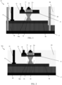
- FIG. 1 shows a structure and respective fabrication processes in accordance with aspects of the present disclosure.
- the structure 10 of FIG. 1 shows a collector 14 with an undercut region (e.g., profile) 14a.
- the collector 14 may be provided between a sub-collector 16, 18, an extrinsic base 20 and an emitter 22.
- the undercut region 14a may be filled with interlevel dielectric material 24 formed by conventional deposition processes, e.g., chemical vapor deposition (CVD).
- An optional deep trench isolation structure 25 may be provided to isolate the device.
- the sub-collector 16, 18 may comprise preferably Si material and, more preferably N+ doped Si material.
- the sub-collector 16 may be doped with phosphorus (e.g., SiP).
- the sub-collector 16 may also be single crystalline semiconductor material with a suitable crystallographic orientation (e.g., a (100), (110), (111), or (001) crystallographic orientation).
- the sub-collector 16 may be formed on a p-type substrate 17 as is known in the art such that no further explanation is required for a complete understanding of the present invention.
- the semiconductor material 18 may be another type of semiconductor material, e.g., SiGe.
- the semiconductor material 18 may be N+ SiGe material epitaxially grown on the sub-collector 16.
- the SiGe material may be in-situ doped with phosphorous (SiGeP), as an example.
- the SiGe material may be implanted or may be doped by out-diffusion from the surrounding regions.
- the sub-collector 16 may comprise both N-type Si as well as N-type SiGe. That is, it is possible that the entire sub-collector region could be SiGe, or it could be just a thin layer of SiGe with N-type Si above and below.
- the at least one layer of N-type SiGe which may be in the collector or sub-collector region, will serve as an etch stop for the undercut recess, e.g., undercut profile 14a as described herein.
- the collector 14 may be a same material as the semiconductor substrate 16.
- the collector 14 may be n-doped Si material.
- the lateral width of the collector 14 is less than a length (or width depending on the perspective view) of the sub-collector material 18 and the intrinsic base 26 or the extrinsic base 20, and the undercut profile 14a is between the sub-collector 18 and the intrinsic base 26 or the extrinsic base 20.
- the undercut profile (e.g., region) 14a of the collector 14 may comprise an narrowed or undercut region, e.g., narrowed profile portion, which is filled with and surrounded by interlevel dielectric material 24.
- the interlevel dielectric material 24 may also be over the semiconductor substrate 16, 18 and surrounding the collector 14, intrinsic base 26, extrinsic base 20 and emitter 22.
- the interlevel dielectric material 24 may be oxide, nitride or combinations thereof.
- the undercut region 14a may comprise a narrow middle portion and wider upper and lower portions.
- the undercut region 14a may include an inwardly tapered sidewall profile from the top to middle portion and from the bottom to the middle portion, resulting in a middle portion having a narrowest cross section along a vertical axis; although other configurations are contemplated herein as further described with respect to the different embodiments shown in FIGS. 4A-4F .
- the undercut region 14a may be formed by a wet or dry etch with a selective chemistry to etch the material of the collector 14. It should be understood by those of skill in the art that the term “taper" can apply to both sharply faceted and rounded recess shapes or combinations thereof.
- the intrinsic base 26 may for formed over the collector 14.
- the intrinsic base 26 may be a p-doped semiconductor material.
- the intrinsic base 26 may be SiGe.
- the intrinsic base 26 may be epitaxially grown from the collector 14 with an in-situ p-type dopant, followed by a conventional patterning process, e.g., lithography and etching (reactive ion etching (RIE) processes).
- RIE reactive ion etching
- the p-type dopant comprises Boron resulting in SiGeB.
- the intrinsic base 26 should be different material than the collector 14 so as to be able to provide the undercut through a selective etching process.
- the extrinsic base 20 may be formed over the intrinsic base 26, surrounding or on sides of the emitter 22.
- the emitter 22 may be formed on the intrinsic base 26 and may be isolated from the extrinsic base 20 by sidewall spacers 22a.
- the sidewall spacers 22a may be a nitride and/or oxide material formed by a conventional deposition process, e.g., CVD, followed by an anisotropic etching process.
- the emitter 22 may comprise an n-doped semiconductor material.
- the dopant may be phosphorous (resulting in SiP) or arsenic (resulting in SiAs).
- the emitter 22 may be formed by conventional epitaxial growth processes with an in-situ doping process as is known in the art.
- the emitter 22 may be formed after the extrinsic base 20.
- the material for the emitter 22 may be deposited in a trench etched through the extrinsic base 20 as is known in the art.
- the extrinsic base 20 may be formed adjacent sides of the sidewall spacers 22a.
- the extrinsic base 20 may be formed by conventional epitaxial growth processes with an in-situ doping process as is known in the art.
- the extrinsic base 20 may be epitaxially grown on the collector 14, with a p-type dopant.
- the p-type dopant comprises Boron resulting in SiB or SiGeB, as examples.
- Suitable semiconductor materials used for the collector 14, sub-collector 16, 18, emitter 22 and bases 20, 26 may be SiGeC, SiC, GE alloys, GaAs, InAs, InP, and other III/V or II/VI compound semiconductors, noting a selectivity should still be present with respect to the collector 14.
- FIG. 1 further shows contacts 28, e.g., wiring structures or interconnect structures, and silicide contacts 30.
- the contacts 28 and silicide contacts 30 may be directly in contact with the sub-collector 18, the emitter 22 and the extrinsic base 20.
- the contacts 28 may be formed through the interlevel dielectric material 24 by conventional lithography, etching and deposition methods known to those of skill in the art.
- a resist formed over the interlevel dielectric material 24 is exposed to energy (light) and developed utilizing a conventional resist developer to form a pattern (opening).
- An etching process with a selective chemistry e.g., reactive ion etching (RIE)
- RIE reactive ion etching
- conductive material e.g., W, Al, Cu with a TiN or TaN liner, for example, can be deposited by any conventional deposition processes, e.g., CVD processes.
- Any residual material on the surface of the insulator interlevel dielectric material 24 can be removed by conventional chemical mechanical polishing (CMP) processes.
- CMP chemical mechanical polishing
- the silicide process begins with deposition of a thin transition metal layer, e.g., nickel, cobalt or titanium, over fully formed and patterned semiconductor devices (e.g., sub-collector 16, the emitter 22 and the extrinsic base 20). After deposition of the material, the structure is heated allowing the transition metal to react with exposed silicon (or other semiconductor material as described herein) in the active regions of the semiconductor device (e.g., sub-collector 16, the emitter 22 and the extrinsic base 20) forming a low-resistance transition metal silicide. Following the reaction, any remaining transition metal is removed by chemical etching, leaving silicide contacts 30 in the active regions of the device.
- a thin transition metal layer e.g., nickel, cobalt or titanium
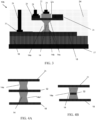
- FIG. 2 shows another structure 10a in accordance with additional aspects of the present disclosure.
- the collector 14 includes the undercut region 14a surrounded by an airgap 15 formed in the interlevel dielectric material 24.
- the airgap 15 preferably extends to the sidewalls of the collector 14.
- the airgap 15 may be formed by a conventional pinch-off process, which is formed during the deposition of the interlevel dielectric material 24 as is known in the art.
- the remaining features of the structure 10a are similar to the structure 10 of FIG. 1 such that no further explanation is required for a complete understanding of the present disclosure.
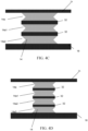
- FIG. 3 shows another structure 10b in accordance with additional aspects of the present disclosure.
- the undercut region 14a includes a straight portion 14b and a tapered portion 14c.
- the tapered portion 14c comprises an inwardly tapered profile from the top to the straight section 14b (at an approximate mid portion) and from the bottom to the to the straight section 14b (at an approximate mid portion).
- the recessed profile may include embodiments that are rounded and/or asymmetric.
- the collector 14 and undercut region 14a may be surrounded by the interlevel dielectric material 24 or an airgap formed in the interlevel dielectric material 24.
- the remaining features of the structure 10b are similar to the structure 10 of FIG. 1 such that no further explanation is required for a complete understanding of the present disclosure.
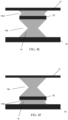
- FIGS. 4A-4F show various profiles of collectors in accordance with aspects of the present disclosure.
- FIG. 4A shows a collector 14 with two recessed portions 14a, 14a1 separated along the vertical axis by a layer of semiconductor material 32.
- the layer of semiconductor material 32 will extend through a wider portion of the collector 14.
- each of the recessed portions 14a, 14a1 include inwardly tapered sidewalls as already described herein.
- the layer of semiconductor material 32 may be semiconductor material that etches selectively with respect to the semiconductor material of the collector 14.
- the layer of semiconductor material 32 may be the same material as the semiconductor material used for the sub-collector 18 and the extrinsic base 28.
- the layer of semiconductor material 32 may be SiGe; whereas the collector 14 may be Si.
- the undercut profile can be precisely tuned to achieve any desired shape. For example, in the embodiment of FIG. 4A , a higher percentage of Ge can be used to provide the desired profile.
- FIG. 4B shows a collector 14 with a recessed portion 14a comprising inwardly tapered sidewalls, as noted in the structures 10, 10a, 10b.
- a layer of semiconductor material 32 may extend through the narrow region of the collector 14, approximately at the center along the vertical axis.
- the undercut profile 14a shown in the embodiment of FIG. 4B can be precisely tuned by providing a lower percentage of Ge in order to obtain the desired shape. In this way, to obtain a wider region of the undercut profile would use a higher percentage of Ge, compared to a lower percentage of Ge for a narrower section of the undercut profile.
- FIGS. 4C and 4D show collectors 14 with multiple recessed portions separated along the vertical axis by one or more layers of semiconductor material 32.
- the collector 14 includes three recessed portions 14a, 14a1, 14a2, each of which are separated from one another in the vertical axis by a layer of semiconductor material 32.
- the collector 14 includes four recessed portions 14a, 14a1, 14a2, 14a3, each of which are separated from one another in the vertical axis by a layer of semiconductor material 32. It should be understood by those of skill in the art that more recessed portions (and respective layers of semiconductor material 32), or layers of different thicknesses, spacing, and/or composition are also contemplated by the present disclosure.
- FIGS. 4E and 4F show collectors 14 with multiple recessed portions asymmetrically positioned in the vertical axis, separated in the vertical direction by a layer of semiconductor material 32.
- the undercut region 14a is smaller than the undercut region 14a1.
- the undercut region 14a1 is closer to the extrinsic base 26 and, in FIG. 4F , the undercut region 14a1 is closer to the sub-collector 18.
- the spacings and positions of the undercut regions 14a, 14a1 along the vertical axis can be tuned by adjusting the location of the layer of semiconductor material 32 within the collector 14.
- SoC system on chip
- the SoC is an integrated circuit (also known as a "chip") that integrates all components of an electronic system on a single chip or substrate. As the components are integrated on a single substrate, SoCs consume much less power and take up much less area than multichip designs with equivalent functionality. Because of this, SoCs are becoming the dominant force in the mobile computing (such as in Smartphones) and edge computing markets. SoC is also used in embedded systems and the Internet of Things.
- the method(s) as described above is used in the fabrication of integrated circuit chips.
- the resulting integrated circuit chips can be distributed by the fabricator in raw wafer form (that is, as a single wafer that has multiple unpackaged chips), as a bare die, or in a packaged form.
- the chip is mounted in a single chip package (such as a plastic carrier, with leads that are affixed to a motherboard or other higher level carrier) or in a multichip package (such as a ceramic carrier that has either or both surface interconnections or buried interconnections).
- the chip is then integrated with other chips, discrete circuit elements, and/or other signal processing devices as part of either (a) an intermediate product, such as a motherboard, or (b) an end product.
- the end product can be any product that includes integrated circuit chips, ranging from toys and other low-end applications to advanced computer products having a display, a keyboard or other input device, and a central processor.
Landscapes
- Bipolar Transistors (AREA)
Abstract
Description
- This invention was made with government support under Contract # HR0011-203-0002 awarded by DARPA-T-MUSIC. The government has certain rights in the invention.
- The present disclosure relates to semiconductor structures and, more particularly, to vertical heterojunction bipolar transistors and methods of manufacture.
- A heterojunction bipolar transistor is a type of bipolar junction transistor which uses differing semiconductor materials for the emitter and base regions, creating a heterojunction. The heterojunction bipolar transistor can handle signals of very high frequencies, up to several hundred GHz. The heterojunction bipolar transistor may be used in modern ultrafast circuits including radio frequency (RF) systems, and in applications requiring a high power efficiency, such as RF power amplifiers in cellular telephones.
- In an aspect of the disclosure, a structure comprises: a sub-collector region; a collector region above the sub-collector region; an intrinsic base above the collector region; an emitter above the intrinsic base region; and an extrinsic base on the intrinsic base and adjacent to the emitter, wherein the collector region includes an undercut profile comprising lower inwardly tapered sidewalls and upper inwardly tapered sidewalls which extend to a narrow section between the sub-collector region and the base region. Additional features of the structure are set forth in dependent claims 2 to 10.
- In an aspect of the disclosure, a structure comprises: a sub-collector region comprising a first semiconductor material; an intrinsic base; an emitter; an extrinsic base on the intrinsic base and adjacent to the emitter; and a collector comprising an undercut profile comprising lower inwardly tapered sidewalls and upper inwardly tapered sidewalls which extending to a narrow section between the sub-collector region and the intrinsic base.
Additional features of the structure are set forth in dependent claims 12 to 14. - In an aspect of the disclosure, a method comprises: forming a sub-collector region; forming a collector above the sub-collector region; forming an intrinsic base above the collector region; forming an emitter above the intrinsic base region; forming an extrinsic base on the intrinsic base and adjacent to the emitter; and forming an undercut in the collector region, the undercut comprising lower inwardly tapered sidewalls and upper inwardly tapered sidewalls which extending to a narrow section between the sub-collector region and the extrinsic base.
- The present disclosure is described in the detailed description which follows, in reference to the noted plurality of drawings by way of non-limiting examples of exemplary embodiments of the present disclosure.
-
FIG. 1 shows a structure and respective fabrication processes in accordance with aspects of the present disclosure. -
FIG. 2 shows a structure and respective fabrication processes in accordance with additional aspects of the present disclosure. -
FIG. 3 shows a structure and respective fabrication processes in accordance with further aspects of the present disclosure. -
FIGS. 4A-4F show various collector profiles in accordance with aspects of the present disclosure. - The present disclosure relates to semiconductor structures and, more particularly, to vertical heterojunction bipolar transistors and methods of manufacture. More specifically, the present disclosure is directed to a vertical heterojunction bipolar transistor with a sidewall undercut (e.g., undercut profile) and methods of manufacture. Advantageously, the present disclosure provides the ability to control and modify a recess structure to achieve a high performance device.
- In embodiments, the high performance device described herein may be a vertical heterojunction bipolar transistor with different collector profiles. The vertical heterojunction bipolar transistor may include, for example, an N+ Si/SiGe sub-collector, an n-type Si collector, a p-SiGe base and an n+ Si emitter; although other materials are contemplated herein. For example, although the high performance device is described with respect to an NPN transistor structure, it should be understood by those of skill in the art that the high performance device can equally be a PNP transistor structure by reversing the doping scheme. An undercut profile may be provided in the collector between the base and sub-collector. A lateral width of the collector is less than sub-collector and base.
- The vertical heterojunction bipolar transistors of the present disclosure can be manufactured in a number of ways using a number of different tools. In general, though, the methodologies and tools are used to form structures with dimensions in the micrometer and nanometer scale. The methodologies, i.e., technologies, employed to manufacture the vertical heterojunction bipolar transistor of the present disclosure have been adopted from integrated circuit (IC) technology. For example, the structures are built on wafers and are realized in films of material patterned by photolithographic processes on the top of a wafer. In particular, the fabrication of the vertical heterojunction bipolar transistors uses three basic building blocks: (i) deposition or growth of thin films of material on a substrate, (ii) applying a patterned mask on top of the films by photolithographic imaging, and (iii) etching the films selectively to the mask. In addition, precleaning processes may be used to clean etched surfaces of any contaminants, as is known in the art. Moreover, when necessary, rapid thermal anneal processes may be used to drive-in dopants or material layers as is known in the art.
-
FIG. 1 shows a structure and respective fabrication processes in accordance with aspects of the present disclosure. In particular, thestructure 10 ofFIG. 1 shows acollector 14 with an undercut region (e.g., profile) 14a. Thecollector 14 may be provided between asub-collector extrinsic base 20 and anemitter 22. Theundercut region 14a may be filled with interleveldielectric material 24 formed by conventional deposition processes, e.g., chemical vapor deposition (CVD). An optional deeptrench isolation structure 25 may be provided to isolate the device. - More specifically, in the
structure 10 ofFIG. 1 , thesub-collector sub-collector 16 may be doped with phosphorus (e.g., SiP). Thesub-collector 16 may also be single crystalline semiconductor material with a suitable crystallographic orientation (e.g., a (100), (110), (111), or (001) crystallographic orientation). As should be understood by those of skill in the art, thesub-collector 16 may be formed on a p-type substrate 17 as is known in the art such that no further explanation is required for a complete understanding of the present invention. - The
semiconductor material 18 may be another type of semiconductor material, e.g., SiGe. In preferred embodiments, thesemiconductor material 18 may be N+ SiGe material epitaxially grown on thesub-collector 16. For example, the SiGe material may be in-situ doped with phosphorous (SiGeP), as an example. Alternatively, the SiGe material may be implanted or may be doped by out-diffusion from the surrounding regions. In embodiments, thesub-collector 16 may comprise both N-type Si as well as N-type SiGe. That is, it is possible that the entire sub-collector region could be SiGe, or it could be just a thin layer of SiGe with N-type Si above and below. It should also be recognized as described herein that the at least one layer of N-type SiGe, which may be in the collector or sub-collector region, will serve as an etch stop for the undercut recess, e.g., undercutprofile 14a as described herein. - The
collector 14 may be a same material as thesemiconductor substrate 16. For example, thecollector 14 may be n-doped Si material. In embodiments, the lateral width of thecollector 14 is less than a length (or width depending on the perspective view) of thesub-collector material 18 and theintrinsic base 26 or theextrinsic base 20, and theundercut profile 14a is between thesub-collector 18 and theintrinsic base 26 or theextrinsic base 20. - The undercut profile (e.g., region) 14a of the
collector 14 may comprise an narrowed or undercut region, e.g., narrowed profile portion, which is filled with and surrounded by interleveldielectric material 24. The interleveldielectric material 24 may also be over thesemiconductor substrate collector 14,intrinsic base 26,extrinsic base 20 andemitter 22. In embodiments, the interleveldielectric material 24 may be oxide, nitride or combinations thereof. - In this embodiment, the
undercut region 14a may comprise a narrow middle portion and wider upper and lower portions. In more specific embodiments, theundercut region 14a may include an inwardly tapered sidewall profile from the top to middle portion and from the bottom to the middle portion, resulting in a middle portion having a narrowest cross section along a vertical axis; although other configurations are contemplated herein as further described with respect to the different embodiments shown inFIGS. 4A-4F . Theundercut region 14a may be formed by a wet or dry etch with a selective chemistry to etch the material of thecollector 14. It should be understood by those of skill in the art that the term "taper" can apply to both sharply faceted and rounded recess shapes or combinations thereof. - Still referring to
FIG. 1 , theintrinsic base 26 may for formed over thecollector 14. In embodiments, theintrinsic base 26 may be a p-doped semiconductor material. In more specific embodiments, theintrinsic base 26 may be SiGe. For example, theintrinsic base 26 may be epitaxially grown from thecollector 14 with an in-situ p-type dopant, followed by a conventional patterning process, e.g., lithography and etching (reactive ion etching (RIE) processes). In preferred embodiments, the p-type dopant comprises Boron resulting in SiGeB. Theintrinsic base 26 should be different material than thecollector 14 so as to be able to provide the undercut through a selective etching process. - The
extrinsic base 20 may be formed over theintrinsic base 26, surrounding or on sides of theemitter 22. Theemitter 22 may be formed on theintrinsic base 26 and may be isolated from theextrinsic base 20 bysidewall spacers 22a. Thesidewall spacers 22a may be a nitride and/or oxide material formed by a conventional deposition process, e.g., CVD, followed by an anisotropic etching process. Theemitter 22 may comprise an n-doped semiconductor material. For example, the dopant may be phosphorous (resulting in SiP) or arsenic (resulting in SiAs). Theemitter 22 may be formed by conventional epitaxial growth processes with an in-situ doping process as is known in the art. In embodiments, theemitter 22 may be formed after theextrinsic base 20. For example, the material for theemitter 22 may be deposited in a trench etched through theextrinsic base 20 as is known in the art. - Following the formation of the
emitter 22, theextrinsic base 20 may be formed adjacent sides of thesidewall spacers 22a. In embodiments, theextrinsic base 20 may be formed by conventional epitaxial growth processes with an in-situ doping process as is known in the art. Theextrinsic base 20 may be epitaxially grown on thecollector 14, with a p-type dopant. In preferred embodiments, the p-type dopant comprises Boron resulting in SiB or SiGeB, as examples. Other examples of suitable semiconductor materials used for thecollector 14, sub-collector 16, 18,emitter 22 andbases collector 14. -
FIG. 1 further showscontacts 28, e.g., wiring structures or interconnect structures, andsilicide contacts 30. Thecontacts 28 andsilicide contacts 30 may be directly in contact with the sub-collector 18, theemitter 22 and theextrinsic base 20. In embodiments, thecontacts 28 may be formed through the interleveldielectric material 24 by conventional lithography, etching and deposition methods known to those of skill in the art. - For example, a resist formed over the interlevel
dielectric material 24 is exposed to energy (light) and developed utilizing a conventional resist developer to form a pattern (opening). An etching process with a selective chemistry, e.g., reactive ion etching (RIE), will be used to transfer the pattern from the photoresist layer to the interleveldielectric material 24 to form one or more trenches in the interleveldielectric material 24 through the openings of the resist. Following the resist removal by a conventional oxygen ashing process or other known stripants, conductive material, e.g., W, Al, Cu with a TiN or TaN liner, for example, can be deposited by any conventional deposition processes, e.g., CVD processes. Any residual material on the surface of the insulatorinterlevel dielectric material 24 can be removed by conventional chemical mechanical polishing (CMP) processes. - Also, as should be understood by those of skill in the art, the silicide process begins with deposition of a thin transition metal layer, e.g., nickel, cobalt or titanium, over fully formed and patterned semiconductor devices (e.g., sub-collector 16, the
emitter 22 and the extrinsic base 20). After deposition of the material, the structure is heated allowing the transition metal to react with exposed silicon (or other semiconductor material as described herein) in the active regions of the semiconductor device (e.g., sub-collector 16, theemitter 22 and the extrinsic base 20) forming a low-resistance transition metal silicide. Following the reaction, any remaining transition metal is removed by chemical etching, leavingsilicide contacts 30 in the active regions of the device. -
FIG. 2 shows anotherstructure 10a in accordance with additional aspects of the present disclosure. In thestructure 10a ofFIG. 2 , thecollector 14 includes the undercutregion 14a surrounded by anairgap 15 formed in the interleveldielectric material 24. Theairgap 15 preferably extends to the sidewalls of thecollector 14. In embodiments, theairgap 15 may be formed by a conventional pinch-off process, which is formed during the deposition of the interleveldielectric material 24 as is known in the art. The remaining features of thestructure 10a are similar to thestructure 10 ofFIG. 1 such that no further explanation is required for a complete understanding of the present disclosure. -
FIG. 3 shows anotherstructure 10b in accordance with additional aspects of the present disclosure. In thestructure 10b ofFIG. 3 , the undercutregion 14a includes astraight portion 14b and a taperedportion 14c. The taperedportion 14c comprises an inwardly tapered profile from the top to thestraight section 14b (at an approximate mid portion) and from the bottom to the to thestraight section 14b (at an approximate mid portion). It should be understood by one skilled in the art that the recessed profile may include embodiments that are rounded and/or asymmetric. In this and other embodiments described herein, thecollector 14 and undercutregion 14a may be surrounded by the interleveldielectric material 24 or an airgap formed in the interleveldielectric material 24. The remaining features of thestructure 10b are similar to thestructure 10 ofFIG. 1 such that no further explanation is required for a complete understanding of the present disclosure. -
FIGS. 4A-4F show various profiles of collectors in accordance with aspects of the present disclosure. For example,FIG. 4A shows acollector 14 with two recessedportions 14a, 14a1 separated along the vertical axis by a layer ofsemiconductor material 32. In embodiments, the layer ofsemiconductor material 32 will extend through a wider portion of thecollector 14. Also, in embodiments, each of the recessedportions 14a, 14a1 include inwardly tapered sidewalls as already described herein. - The layer of
semiconductor material 32, as with each of the undercut profiles described with respect toFIGS. 4A-4F , may be semiconductor material that etches selectively with respect to the semiconductor material of thecollector 14. In embodiments, the layer ofsemiconductor material 32 may be the same material as the semiconductor material used for the sub-collector 18 and theextrinsic base 28. For example, the layer ofsemiconductor material 32 may be SiGe; whereas thecollector 14 may be Si. Also, it should be understood by those of skill in the art that by including one or more SiGe layers with a lower or higher percentage Ge material, by varying the spacing of thelayer 32, percentage of Ge, or thickness, the undercut profile can be precisely tuned to achieve any desired shape. For example, in the embodiment ofFIG. 4A , a higher percentage of Ge can be used to provide the desired profile. -
FIG. 4B shows acollector 14 with a recessedportion 14a comprising inwardly tapered sidewalls, as noted in thestructures semiconductor material 32 may extend through the narrow region of thecollector 14, approximately at the center along the vertical axis. Also, as should now be understood, the undercutprofile 14a shown in the embodiment ofFIG. 4B can be precisely tuned by providing a lower percentage of Ge in order to obtain the desired shape. In this way, to obtain a wider region of the undercut profile would use a higher percentage of Ge, compared to a lower percentage of Ge for a narrower section of the undercut profile. -
FIGS. 4C and 4D show collectors 14 with multiple recessed portions separated along the vertical axis by one or more layers ofsemiconductor material 32. For example, inFIG. 4C , thecollector 14 includes three recessedportions 14a, 14a1, 14a2, each of which are separated from one another in the vertical axis by a layer ofsemiconductor material 32. InFIG. 4D , thecollector 14 includes four recessedportions 14a, 14a1, 14a2, 14a3, each of which are separated from one another in the vertical axis by a layer ofsemiconductor material 32. It should be understood by those of skill in the art that more recessed portions (and respective layers of semiconductor material 32), or layers of different thicknesses, spacing, and/or composition are also contemplated by the present disclosure. -
FIGS. 4E and 4F showcollectors 14 with multiple recessed portions asymmetrically positioned in the vertical axis, separated in the vertical direction by a layer ofsemiconductor material 32. For example, in bothFIGS. 4E and 4F , the undercutregion 14a is smaller than the undercut region 14a1. InFIG. 4E , the undercut region 14a1 is closer to theextrinsic base 26 and, inFIG. 4F , the undercut region 14a1 is closer to the sub-collector 18. The spacings and positions of the undercutregions 14a, 14a1 along the vertical axis can be tuned by adjusting the location of the layer ofsemiconductor material 32 within thecollector 14. - The structures can be utilized in system on chip (SoC) technology. The SoC is an integrated circuit (also known as a "chip") that integrates all components of an electronic system on a single chip or substrate. As the components are integrated on a single substrate, SoCs consume much less power and take up much less area than multichip designs with equivalent functionality. Because of this, SoCs are becoming the dominant force in the mobile computing (such as in Smartphones) and edge computing markets. SoC is also used in embedded systems and the Internet of Things.
- The method(s) as described above is used in the fabrication of integrated circuit chips. The resulting integrated circuit chips can be distributed by the fabricator in raw wafer form (that is, as a single wafer that has multiple unpackaged chips), as a bare die, or in a packaged form. In the latter case the chip is mounted in a single chip package (such as a plastic carrier, with leads that are affixed to a motherboard or other higher level carrier) or in a multichip package (such as a ceramic carrier that has either or both surface interconnections or buried interconnections). In any case the chip is then integrated with other chips, discrete circuit elements, and/or other signal processing devices as part of either (a) an intermediate product, such as a motherboard, or (b) an end product. The end product can be any product that includes integrated circuit chips, ranging from toys and other low-end applications to advanced computer products having a display, a keyboard or other input device, and a central processor.
- The descriptions of the various embodiments of the present disclosure have been presented for purposes of illustration, but are not intended to be exhaustive or limited to the embodiments disclosed. Many modifications and variations will be apparent to those of ordinary skill in the art without departing from the scope and spirit of the described embodiments. The terminology used herein was chosen to best explain the principles of the embodiments, the practical application or technical improvement over technologies found in the marketplace, or to enable others of ordinary skill in the art to understand the embodiments disclosed herein.
Claims (15)
- A structure comprising:a sub-collector region;a collector region above the sub-collector region;an intrinsic base above the collector region;an emitter above the intrinsic base region; andan extrinsic base on the intrinsic base and adjacent to the emitter,wherein the collector region includes an undercut profile comprising lower inwardly tapered sidewalls and upper inwardly tapered sidewalls which extend to a narrow section between the sub-collector region and the base region.
- The structure of claim 1, wherein the sub-collector region and the intrinsic base comprise a semiconductor material which is different than a semiconductor material of the collector, and, optionally, wherein the semiconductor material of the sub-collector comprises at least n-type SiGe, the intrinsic base comprises p-type SiGe and the collector comprises n-type Si.
- The structure of claim 1 or claim 2, wherein the undercut profile comprises lower inwardly tapered sidewalls and upper inwardly tapered sidewalls which extending to a narrow section between the sub-collector region and the extrinsic base.
- The structure of one of claims 1 to 3, wherein the narrow section comprises a straight sidewall profile.
- The structure of one of claims 1 to 4, further comprising a layer of semiconductor material extending through the narrow section of the collector, which is different than a semiconductor material of the collector region.
- The structure of one of claims 1 to 4, wherein the undercut profile comprises two recessed portions separated along a vertical axis by a layer of semiconductor material that is different than a semiconductor material of the collector, and, optionally, wherein the layer of semiconductor material is a same semiconductor material as the sub-collector.
- The structure of claim 6, wherein the layer of semiconductor material extends through a wider portion of the undercut profile of the collector.
- The structure of one of claims 1 to 4, wherein the undercut profile comprises multiple recessed portions.
- The structure of claim 8, wherein each of the multiple recessed portions are separated along a vertical axis by a semiconductor material that is different than a semiconductor material of the collector, and/or wherein each of the multiple recessed portions are asymmetrically positioned along the vertical axis.
- The structure of one of claims 1 to 9, further comprising an airgap extending to the upper and lower inwardly tapered sidewalls, and further surrounding the undercut profile.
- A structure comprising:a sub-collector region comprising a first semiconductor material;an intrinsic base;an emitter;an extrinsic base on the intrinsic base and adjacent to the emitter; anda collector comprising an undercut profile comprising lower inwardly tapered sidewalls and upper inwardly tapered sidewalls which extending to a narrow section between the sub-collector region and the intrinsic base.
- The structure of claim 11, wherein the first semiconductor material comprises SiGe, the intrinsic base comprise p-type doped SiGe and the sub-collector region comprises n-type doped SiGe and the semiconductor material of the collector comprises Si, and/or wherein the sub-collector region comprises both Si material and SiGe material, with the SiGe material being an etch stop layer.
- The structure of claim 11 or claim 12, wherein the narrow section comprises a straight sidewall profile, and/or wherein the structure further comprises an airgap surrounding the undercut profile.
- The structure of one of claims 11 to 13, wherein the undercut profile comprises multiple recessed portions each of which are separated along a vertical axis by a layer of semiconductor material that is different than a semiconductor material of the collector.
- A method comprising:forming a sub-collector region;forming a collector above the sub-collector region;forming an intrinsic base above the collector region;forming an emitter above the intrinsic base region;forming an extrinsic base on the intrinsic base and adjacent to the emitter; andforming an undercut in the collector region, the undercut comprising lower inwardly tapered sidewalls and upper inwardly tapered sidewalls which extending to a narrow section between the sub-collector region and the extrinsic base.
Applications Claiming Priority (1)
| Application Number | Priority Date | Filing Date | Title |
|---|---|---|---|
| US18/512,859 US20250169087A1 (en) | 2023-11-17 | 2023-11-17 | Vertical heterojunction bipolar transistor |
Publications (1)
| Publication Number | Publication Date |
|---|---|
| EP4557376A1 true EP4557376A1 (en) | 2025-05-21 |
Family
ID=91470060
Family Applications (1)
| Application Number | Title | Priority Date | Filing Date |
|---|---|---|---|
| EP24181005.0A Pending EP4557376A1 (en) | 2023-11-17 | 2024-06-10 | Vertical heterojunction bipolar transistor |
Country Status (5)
| Country | Link |
|---|---|
| US (1) | US20250169087A1 (en) |
| EP (1) | EP4557376A1 (en) |
| KR (1) | KR102867594B1 (en) |
| CN (1) | CN120035156A (en) |
| TW (1) | TW202537407A (en) |
Citations (6)
| Publication number | Priority date | Publication date | Assignee | Title |
|---|---|---|---|---|
| KR20030073771A (en) * | 2002-03-13 | 2003-09-19 | 주식회사 엘지이아이 | Method of manufacturing heterojunction bipolar transistor |
| US6737684B1 (en) * | 1998-02-20 | 2004-05-18 | Matsushita Electric Industrial Co., Ltd. | Bipolar transistor and semiconductor device |
| US8476675B2 (en) * | 2008-02-28 | 2013-07-02 | Nxp B.V. | Semiconductor device and method of manufacture thereof |
| US20150206959A1 (en) * | 2013-10-22 | 2015-07-23 | International Business Machines Corporation | Formation of a high aspect ratio trench in a semiconductor substrate and a bipolar semiconductor device having a high aspect ratio trench isolation region |
| US10672872B1 (en) * | 2019-02-13 | 2020-06-02 | International Business Machines Corporation | Self-aligned base contacts for vertical fin-type bipolar junction transistors |
| US20210257454A1 (en) * | 2020-02-14 | 2021-08-19 | Globalfoundries U.S. Inc. | Heterojunction bipolar transistors with one or more sealed airgap |
Family Cites Families (16)
| Publication number | Priority date | Publication date | Assignee | Title |
|---|---|---|---|---|
| US5298438A (en) * | 1992-08-31 | 1994-03-29 | Texas Instruments Incorporated | Method of reducing extrinsic base-collector capacitance in bipolar transistors |
| KR100456037B1 (en) * | 2001-10-24 | 2004-11-15 | 한국과학기술원 | Method for fabricating Heterojunction Bipolar Transistor using lateral-reverse selective etching of collector |
| US7679164B2 (en) * | 2007-01-05 | 2010-03-16 | International Business Machines Corporation | Bipolar transistor with silicided sub-collector |
| US8975146B2 (en) * | 2013-05-01 | 2015-03-10 | International Business Machines Corporation | Trench isolation structures and methods for bipolar junction transistors |
| US9324846B1 (en) * | 2015-01-08 | 2016-04-26 | Globalfoundries Inc. | Field plate in heterojunction bipolar transistor with improved break-down voltage |
| US10109724B2 (en) * | 2017-02-22 | 2018-10-23 | Qualcomm Incorporated | Heterojunction bipolar transistor unit cell and power stage for a power amplifier |
| US10134880B2 (en) * | 2017-03-29 | 2018-11-20 | Globalfoundries Inc. | Self-aligned bipolar junction transistors with a base grown in a dielectric cavity |
| US10593659B2 (en) * | 2017-03-30 | 2020-03-17 | International Business Machines Corporation | Deep high capacity capacitor for bulk substrates |
| JP2019102639A (en) * | 2017-12-01 | 2019-06-24 | 株式会社村田製作所 | Semiconductor device |
| US11063139B2 (en) * | 2019-09-23 | 2021-07-13 | Globalfoundries U.S. Inc. | Heterojunction bipolar transistors with airgap isolation |
| US11362201B1 (en) * | 2020-12-14 | 2022-06-14 | Globalfoundries U.S. Inc. | Heterojunction bipolar transistors with undercut extrinsic base regions |
| US11411080B2 (en) * | 2021-01-05 | 2022-08-09 | Win Semiconductors Corp. | Heterojunction bipolar transistor and method for forming the same |
| US12046633B2 (en) * | 2021-01-25 | 2024-07-23 | Globalfoundries U.S. Inc. | Airgap structures in auto-doped region under one or more transistors |
| US11888050B2 (en) * | 2021-08-27 | 2024-01-30 | Globalfoundries U.S. Inc. | Lateral bipolar transistor structure with inner and outer spacers and methods to form same |
| US11990536B2 (en) * | 2021-12-31 | 2024-05-21 | Nxp B.V. | Bipolar transistors with multilayer collectors |
| US20250261387A1 (en) * | 2024-02-09 | 2025-08-14 | Taiwan Semiconductor Manufacturing Company Limited | Semiconductor structure and method of manufacture |
-
2023
- 2023-11-17 US US18/512,859 patent/US20250169087A1/en active Pending
-
2024
- 2024-06-10 EP EP24181005.0A patent/EP4557376A1/en active Pending
- 2024-09-18 CN CN202411299364.4A patent/CN120035156A/en active Pending
- 2024-10-17 TW TW113139476A patent/TW202537407A/en unknown
- 2024-10-17 KR KR1020240141947A patent/KR102867594B1/en active Active
Patent Citations (6)
| Publication number | Priority date | Publication date | Assignee | Title |
|---|---|---|---|---|
| US6737684B1 (en) * | 1998-02-20 | 2004-05-18 | Matsushita Electric Industrial Co., Ltd. | Bipolar transistor and semiconductor device |
| KR20030073771A (en) * | 2002-03-13 | 2003-09-19 | 주식회사 엘지이아이 | Method of manufacturing heterojunction bipolar transistor |
| US8476675B2 (en) * | 2008-02-28 | 2013-07-02 | Nxp B.V. | Semiconductor device and method of manufacture thereof |
| US20150206959A1 (en) * | 2013-10-22 | 2015-07-23 | International Business Machines Corporation | Formation of a high aspect ratio trench in a semiconductor substrate and a bipolar semiconductor device having a high aspect ratio trench isolation region |
| US10672872B1 (en) * | 2019-02-13 | 2020-06-02 | International Business Machines Corporation | Self-aligned base contacts for vertical fin-type bipolar junction transistors |
| US20210257454A1 (en) * | 2020-02-14 | 2021-08-19 | Globalfoundries U.S. Inc. | Heterojunction bipolar transistors with one or more sealed airgap |
Also Published As
| Publication number | Publication date |
|---|---|
| TW202537407A (en) | 2025-09-16 |
| US20250169087A1 (en) | 2025-05-22 |
| KR102867594B1 (en) | 2025-10-13 |
| KR20250072861A (en) | 2025-05-26 |
| CN120035156A (en) | 2025-05-23 |
Similar Documents
| Publication | Publication Date | Title |
|---|---|---|
| US20190181250A1 (en) | Compact device structures for a bipolar junction transistor | |
| US11276770B2 (en) | Gate controlled lateral bipolar junction/heterojunction transistors | |
| US12349375B2 (en) | Lateral bipolar transistors with gate structure aligned to extrinsic base | |
| US11145725B2 (en) | Heterojunction bipolar transistor | |
| EP4525048A1 (en) | Bipolar transistors | |
| US12336243B2 (en) | Lateral bipolar transistor with gated collector | |
| EP4216280A1 (en) | Vertical bipolar transistors on soi substrates with the collectors in the buried oxide | |
| US20250169087A1 (en) | Vertical heterojunction bipolar transistor | |
| US12009412B2 (en) | Bipolar transistors | |
| US20230352570A1 (en) | Bipolar junction transistor | |
| US11855195B2 (en) | Transistor with wrap-around extrinsic base | |
| US11916135B2 (en) | Bipolar transistor | |
| US11804542B2 (en) | Annular bipolar transistors | |
| US11837460B2 (en) | Lateral bipolar transistor | |
| US20260090381A1 (en) | Heterojunction bipolar transistor | |
| EP4276911A1 (en) | Heterojunction bipolar transistors | |
| US12040388B2 (en) | Lateral bipolar transistors | |
| US12278269B2 (en) | Bipolar transistor with stepped emitter | |
| US11935927B2 (en) | Bipolar transistor with collector contact | |
| EP4683454A1 (en) | Vertical heterojunction bipolar transistor with laterally recessed collector and a semiconductor liner on sidewalls of the collector | |
| US20260026023A1 (en) | Vertical heterojunction bipolar transistor | |
| US11177345B1 (en) | Heterojunction bipolar transistor | |
| CN117995894A (en) | Heterojunction bipolar transistor with amorphous semiconductor region |
Legal Events
| Date | Code | Title | Description |
|---|---|---|---|
| PUAI | Public reference made under article 153(3) epc to a published international application that has entered the european phase |
Free format text: ORIGINAL CODE: 0009012 |
|
| STAA | Information on the status of an ep patent application or granted ep patent |
Free format text: STATUS: THE APPLICATION HAS BEEN PUBLISHED |
|
| AK | Designated contracting states |
Kind code of ref document: A1 Designated state(s): AL AT BE BG CH CY CZ DE DK EE ES FI FR GB GR HR HU IE IS IT LI LT LU LV MC ME MK MT NL NO PL PT RO RS SE SI SK SM TR |
|
| STAA | Information on the status of an ep patent application or granted ep patent |
Free format text: STATUS: REQUEST FOR EXAMINATION WAS MADE |
|
| 17P | Request for examination filed |
Effective date: 20251015 |
|
| STAA | Information on the status of an ep patent application or granted ep patent |
Free format text: STATUS: EXAMINATION IS IN PROGRESS |
|
| 17Q | First examination report despatched |
Effective date: 20260102 |