EP4556891A1 - Method and device for simplified determination of effective electron lifetime - Google Patents
Method and device for simplified determination of effective electron lifetime Download PDFInfo
- Publication number
- EP4556891A1 EP4556891A1 EP23306983.0A EP23306983A EP4556891A1 EP 4556891 A1 EP4556891 A1 EP 4556891A1 EP 23306983 A EP23306983 A EP 23306983A EP 4556891 A1 EP4556891 A1 EP 4556891A1
- Authority
- EP
- European Patent Office
- Prior art keywords
- light beam
- excitation light
- pulses
- pulse
- effective electron
- Prior art date
- Legal status (The legal status is an assumption and is not a legal conclusion. Google has not performed a legal analysis and makes no representation as to the accuracy of the status listed.)
- Granted
Links
Images

Classifications
-
- G—PHYSICS
- G01—MEASURING; TESTING
- G01N—INVESTIGATING OR ANALYSING MATERIALS BY DETERMINING THEIR CHEMICAL OR PHYSICAL PROPERTIES
- G01N21/00—Investigating or analysing materials by the use of optical means, i.e. using sub-millimetre waves, infrared, visible or ultraviolet light
- G01N21/62—Systems in which the material investigated is excited whereby it emits light or causes a change in wavelength of the incident light
- G01N21/63—Systems in which the material investigated is excited whereby it emits light or causes a change in wavelength of the incident light optically excited
- G01N21/64—Fluorescence; Phosphorescence
- G01N21/6489—Photoluminescence of semiconductors
-
- G—PHYSICS
- G01—MEASURING; TESTING
- G01N—INVESTIGATING OR ANALYSING MATERIALS BY DETERMINING THEIR CHEMICAL OR PHYSICAL PROPERTIES
- G01N21/00—Investigating or analysing materials by the use of optical means, i.e. using sub-millimetre waves, infrared, visible or ultraviolet light
- G01N21/62—Systems in which the material investigated is excited whereby it emits light or causes a change in wavelength of the incident light
- G01N21/63—Systems in which the material investigated is excited whereby it emits light or causes a change in wavelength of the incident light optically excited
- G01N21/64—Fluorescence; Phosphorescence
- G01N21/6408—Fluorescence; Phosphorescence with measurement of decay time, time resolved fluorescence
Definitions
- the present invention relates to techniques for determining effective electron lifetime, or effective carrier lifetime, in components.
- the invention is of particular, non-limiting interest in the photovoltaic industry.
- Effective electron lifetime measurement techniques are commonly used to control the quality of photovoltaic components during the manufacturing process.
- MPL photoluminescence
- the invention is generally aimed at simplifying the known techniques for determining effective electron lifetime.
- the method of the invention comprises the following steps:
- said excitation light beam comprises several pulses that are temporally spaced from one another and that have respective absolute maximum amplitudes different from one another.
- each or at least one of said pulses may have a respective absolute maximum amplitude that is different from the absolute maximum amplitude of the other pulses.
- each or at least one of said pulses of the excitation light beam is a Gaussian pulse.
- the step for calculating said effective electron lifetime value comprises, for each or at least one of said pulses of the excitation light beam, determining a plurality of mean amplitude difference values between the excitation light beam pulse and the corresponding photoluminescence light pulse.
- Each or at least one of said mean amplitude difference values can be related to a respective temporal shift of these pulses one with respect to the other.
- the step for calculating said effective electron lifetime value comprises, for each or at least one of said pulses of the excitation light beam, determining said effective electron lifetime value based on the minimum of said mean amplitude difference values.
- the effective electron lifetime value corresponds to the temporal shift associated with the minimum of said mean amplitude difference values.
- said excitation light beam comprises several plateaux, each or at least one of said pulses of the excitation light beam being generated from one respective of these plateaux.
- each pulse can come out of a respective plateau preferably remaining within a quasi-steady-state regime.
- the amplitude of each or at least one of said pulses of the excitation light beam relative to its corresponding plateau is equal to a predetermined value.
- said predetermined value is equal from one of said pulses to the other.
- said component to be analysed forms, or is intended to form, a photovoltaic cell element.
- the invention provides a device for determining effective electron lifetime in a component to be analysed.
- the device of the invention can be specifically configured for carrying out a method as defined above.
- the device of the invention comprises:
- the invention provides a computer program comprising instructions to cause a device as defined above to execute the steps of a method as defined above.
- the invention provides a computer-readable medium having stored thereon a computer program as defined above.
- the present invention simplifies the determination of effective electron lifetime, allows fast measurements and lowers the hardware requirements for processing the data.
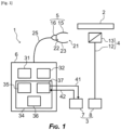
- Figure 1 shows schematically a device 1 in accordance with the invention, for determining effective electron lifetime in a component 2 to be analysed.
- the device 1 of figure 1 is adapted to operate in situ.
- the component 2 also called “sample” generally forms an area of interest, for example of a circuitry, such as a semiconductor area.
- the component 2 is a part of an assembly of layers forming a photovoltaic cell.
- the effective electron lifetime is the amount of time an electron remains within the conduction band between photon absorption - in particular photon with higher energy than band gap - and photon emission at the bandgap energy.
- the device 1 comprises a light generator 3, an optical system 4, a detector 5, and a processing unit 6.
- the light generator 3 comprises a command unit 7 and a light source 8.
- the light source 8 is a laser source, comprising for example a laser diode.
- the light source 8 is configured to generate an excitation light beam, and more particularly an excitation light beam signal 10 as illustrated in figure 2 (see further below).
- the optical system 4 is configured to transport said excitation light beam emitted by the light source 8 towards the component 2.
- the optical system 4 comprises a fibre 12 and a separator 13.
- the fibre 12 is configured to convey the excitation light beam from an output of the light source to the separator 13.
- the separator 13 is a shortpass Dichroic filter with a cute-off wavelength.
- the separator 13 of figure 1 defines a transmitting light path and a reflecting light path according to the wavelength.
- the transmitting path is for light below cut-of wavelength.
- the reflecting path is for light with a higher wavelength than the cut-off wavelength.
- the cut-off wavelength is equal to 950 nm.
- the separator 13 is configured so that the transmitting path corresponds to a light outputted from the fibre 12 and sent towards the component 2, while the reflecting path corresponds to a light coming from the component 2 and sent to the detector 5.
- the detector 5 comprises a compound parabolic concentrator 15 and a photodetector 16.
- a compound parabolic concentrator is a reflective, non-imaging optical device, which employs specifically configured parabolic properties to take advantage of the maximum concentration of light energy.
- the compound parabolic concentrator 15 defines an input end 21, an output end 22, and a wall 23 having a parabolic shape and connecting the ends 21 and 22 to each other.
- the input end 21 is larger than the output end 22 to collect efficiently divergent light, which is then reflected and concentrated by the wall 23.
- Such a concentrator 15 enables to collect at the output end 22 a relatively large part of the photoluminescence light emitted by the component 2.
- the concentrator 15 may have an optical filter (not shown), for example a 785 nm laser line filter, at the input end 21.
- the photodetector 16 of the detector 5 of figure 1 is positioned at the output end 22 of the compound parabolic concentrator 15.
- the photodetector 16 comprises an InGaAs photodiode.
- this unit 6 is connected to the photodetector 16 with a coaxial cable 25.
- the processing unit 6 comprises a calculator 31 and data storage components 32.
- the calculator 31 may comprise a monocore or multicore processor - such as a CPU, a GPU, a microcontroller, and/or a DSP -, a programmable logic circuitry - such as an ASIC, a FPGA, a PLD, and/or a PLA -, a state machine, gated logic and/or discrete hardware components.
- a monocore or multicore processor - such as a CPU, a GPU, a microcontroller, and/or a DSP -
- a programmable logic circuitry - such as an ASIC, a FPGA, a PLD, and/or a PLA -
- a state machine gated logic and/or discrete hardware components.
- the processing unit 6 comprises an electronic processing subunit 34 comprising an amplifier 35, a low-pass filter 36 and a voltage data logger 37 having the role of a function generator.
- the voltage data logger 37 is configured to send data to the command unit 7, via a coaxial cable 41, to modify parameters of the excitation light beam signal generated by the generator 3, and to record the signal of the light source 8 via another coaxial cable 42.
- a signal 10 is depicted on a graph where the abscissa X1 corresponds to time and the ordinate X2 corresponds to amplitude, or intensity.
- the signal 10 of figure 2 comprises several pulses 50 and several plateaux 51.
- the plateaux 51 are temporally spaced from one another and each of them has a respective absolute amplitude.
- the absolute amplitude of the plateaux 51 increases from one plateau to the next, according to a linear function.
- the pulses 50 are respectively associated with these plateaux 51. More specifically, each of said pulses 50 is generated from a respective plateau 51, so that the absolute amplitude at which the pulses 50 are generated also increases from one pulse to the next according to X1.
- each of said pulses 50 is a Gaussian pulse.
- the ratio of the amplitude C to the width of each pulse 50 can be about eight to one.
- the width of the pulse 50 is selected to be greater than the effective electron lifetime values to be determined, for example up to twenty times greater.
- maximum measurement speed can be determined based on the expected effective electron lifetime values.
- the values C and D are common to all the pulses 50.
- each of said pulses 50 of the signal 10 i.e., its maximum amplitude relative to its corresponding plateau 51
- each of said pulses 50 has a respective absolute maximum amplitude that is different from the absolute maximum amplitude of the other pulses 50.
- the absolute maximum amplitude of the pulses 50 of the signal 10 increases over time, i.e., from one pulse to the next, according to a linear function.
- the signal 10 can have a number of pulses 50 per second in the range from 1 to 10, and their width can be comprised between 0.005 s and 0.02 s.
- the signal 10 of figure 2 here constitutes an excitation light beam that can be used in methods and devices according to the invention.
- the device 1 of figure 1 is used so that the light source 8 emits an excitation light beam that corresponds to the signal 10 of figure 2 , and the detector 5 detects a corresponding photoluminescence light.
- Figure 3 shows a temporal portion of these excitation light beam 10 and corresponding normalized photoluminescence light signal 58.
- the photoluminescence light signal 58 being emitted in response to the excitation light beam 10, its shape is generally similar to that of the excitation light beam 10.
- the photoluminescence light signal 58 is thus provided with pulses 60 and plateaux 61 similar to that of the excitation light beam 10.
- the above description of figure 2 applies mutatis mutandis.
- Figure 3 shows more specifically two pulses 50 and two respective plateaux 51 of the excitation light beam 10, as well as two corresponding pulses 60 and two respective plateaux 61 of the photoluminescence light signal 58.
- a step for calculating an effective electron lifetime value is performed for each of the pulses 50 of the excitation light beam 10, using in this example the processing unit 6.
- effective electron lifetime values are based on a temporal shift between two corresponding pulses 50 and 60.
- the calculation step comprises an iteration of the following steps for each couple of pulses 50 and 60.
- a first effective electron lifetime value is calculated based on a temporal shift between the pulses 50 and 60 at the left of figure 3 , called first pulses 50 and 60.
- a plurality of mean amplitude difference values between these first pulses 50 and 60 is determined.
- Each of said mean amplitude difference values is related to a respective temporal shift of these first pulses 50 and 60, one with respect to the other.
- An effective electron lifetime value is then determined based on the minimum of said mean amplitude difference values.
- the effective electron lifetime value here corresponds to the temporal shift associated with the minimum of said mean amplitude difference values.
- the principle of the invention as defined in the claims, and more specifically the calculation of any effective electron lifetime value can be carried out using an excitation light beam having other parameters than the signal of figure 2 .
- the excitation light beam can comprise one or more asymmetric pulses and/or that are respectively generated at varying maximum absolute and/or relative amplitudes according to any function or randomly.
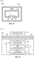
- Figure 4 illustrates a specific use of a device according to the invention, in this example of the device 1 of figure 1 , for measuring effective electron lifetime in the component 2 within a reactor 100.
- the reactor 100 is an apparatus in which circuitry is built, for example a "PECVD" (for plasma-enhanced chemical vapor deposition) reactor as known per se in the art.
- PECVD plasma-enhanced chemical vapor deposition
- the reactor 100 comprises an inner chamber 101 and an external chamber 102 into which the inner chamber 101 is located.
- the component 2 to be analysed is received in the inner chamber 101 and the reactor 100 is adapted for interacting with the device 1 of the invention as described below.
- the inner chamber 101 comprises a sample holder 103 and an observation aperture 104 upon which the component 2 is placed.
- a window 105 of the external chamber 102 defines an access to the observation aperture 104.
- the window 105 is configured to allow illuminating the component 2 with an excitation light beam and collecting a photoluminescence light emitted by the component 2 in response to the excitation light beam, according to the above-described method and using the device 1 of figure 1 .
- the invention generally relates to a method comprising a step S1 where a sample as the above-described component 2 is illuminated, and a step S2 where one or more effective electron lifetime values are calculated.
- Step S1 can be carried out using the light generator 3 of the device 1 of figure 2 , to emit for example an excitation light beam as illustrated in figure 2 .
- Step S2 generally comprises steps S3 and S4 for recording the excitation light beam signal and a response signal, the latter corresponding in this case to the above-described photoluminescence light emitted by the sample in response to the excitation light beam.
- Step S2 also comprises one or more iterations I1 of steps S5, S6 and S7.
- step S5 a pulse of the excitation signal is selected.
- step S6 two corresponding pulses of the excitation signal and the response signal, respectively, are shifted and an amplitude difference between these pulses is calculated in step S7.
- Iterations I2 of steps S6 and S7 are performed to find the optimum overlap of corresponding pulses.
- Step S2 can be carried out according to the above-described technique.
Landscapes
- Health & Medical Sciences (AREA)
- Nuclear Medicine, Radiotherapy & Molecular Imaging (AREA)
- Physics & Mathematics (AREA)
- Life Sciences & Earth Sciences (AREA)
- Chemical & Material Sciences (AREA)
- Analytical Chemistry (AREA)
- Biochemistry (AREA)
- General Health & Medical Sciences (AREA)
- General Physics & Mathematics (AREA)
- Immunology (AREA)
- Pathology (AREA)
- Investigating, Analyzing Materials By Fluorescence Or Luminescence (AREA)
Abstract
Description
- The present invention relates to techniques for determining effective electron lifetime, or effective carrier lifetime, in components.
- The invention is of particular, non-limiting interest in the photovoltaic industry.
- Effective electron lifetime measurement techniques are commonly used to control the quality of photovoltaic components during the manufacturing process.
- Contactless methods and specifically modulated photoluminescence (MPL) techniques have been developed for carrying out such measurements, as described for example in the documents
EP4257958A1 andEP3767282A1 . Generally, MPL techniques involve measuring phase shifts between an excitation frequency-modulated signal and a corresponding emitted photoluminescence signal. - Known MPL techniques are powerful but involve complex calculations to determine effective electron lifetime.
- The invention is generally aimed at simplifying the known techniques for determining effective electron lifetime.
- According to an aspect of the invention, it is provided a method for determining effective electron lifetime in a component to be analysed.
- The method of the invention comprises the following steps:
- emitting an excitation light beam comprising one or several pulses,
- detecting a photoluminescence light emitted by the component in response to the excitation light beam,
- for each or at least one of said pulses of the excitation light beam, calculating an effective electron lifetime value based on a temporal shift between this pulse and a corresponding pulse of the photoluminescence light.
- In an embodiment, said excitation light beam comprises several pulses that are temporally spaced from one another and that have respective absolute maximum amplitudes different from one another.
- In other words, each or at least one of said pulses may have a respective absolute maximum amplitude that is different from the absolute maximum amplitude of the other pulses.
- In an embodiment, each or at least one of said pulses of the excitation light beam is a Gaussian pulse.
- In an embodiment, the step for calculating said effective electron lifetime value comprises, for each or at least one of said pulses of the excitation light beam, determining a plurality of mean amplitude difference values between the excitation light beam pulse and the corresponding photoluminescence light pulse.
- Each or at least one of said mean amplitude difference values can be related to a respective temporal shift of these pulses one with respect to the other.
- In an embodiment, the step for calculating said effective electron lifetime value comprises, for each or at least one of said pulses of the excitation light beam, determining said effective electron lifetime value based on the minimum of said mean amplitude difference values.
- In an embodiment, each or at least one of said mean amplitude difference values is calculated using the following formula:

- In an embodiment, for each or at least one of said pulses of the excitation light beam, the effective electron lifetime value corresponds to the temporal shift associated with the minimum of said mean amplitude difference values.
- In an embodiment, said excitation light beam comprises several plateaux, each or at least one of said pulses of the excitation light beam being generated from one respective of these plateaux.
- In other words, each pulse can come out of a respective plateau preferably remaining within a quasi-steady-state regime.
- In other words, a pulse temporally succeeds a first plateau region and is followed by a second plateau region of some amplitude as the first plateau region.
- In an embodiment, the amplitude of each or at least one of said pulses of the excitation light beam relative to its corresponding plateau is equal to a predetermined value.
- In an embodiment, said predetermined value is equal from one of said pulses to the other.
- In an embodiment, said component to be analysed forms, or is intended to form, a photovoltaic cell element.
- According to another aspect, the invention provides a device for determining effective electron lifetime in a component to be analysed.
- The device of the invention can be specifically configured for carrying out a method as defined above.
- The device of the invention comprises:
- a light source configured to emit an excitation light beam comprising one or several pulses,
- a detector configured to detect a photoluminescence light emitted by the component in response to the excitation light beam,
- a processing unit configured to calculate, for each or at least one of said pulses of the excitation light beam, an effective electron lifetime value based on a temporal shift between this pulse and a corresponding pulse of the photoluminescence light.
- According to another aspect, the invention provides a computer program comprising instructions to cause a device as defined above to execute the steps of a method as defined above.
- According to a further aspect, the invention provides a computer-readable medium having stored thereon a computer program as defined above.
- The present invention simplifies the determination of effective electron lifetime, allows fast measurements and lowers the hardware requirements for processing the data.
- The present invention, and all its aspects, embodiments and advantages associated therewith will become more readily apparent in view of the detailed description of particular embodiments provided below, including the accompanying drawings.
- The following, non-limiting, embodiments of the invention are described with reference to the accompanying drawings in which:
-
Figure 1 is a schematic representation of a device according to the invention, for determining effective electron lifetime in a component to be analysed; -
Figure 2 is a signal forming an excitation light beam that can be generated according to the invention; -
Figure 3 shows a portion of the signal offigure 2 and a corresponding portion of a response photoluminescence light that is collected according to the invention; -
Figure 4 is a schematic representation of a PECVD reactor for determining effective electron lifetime in a component according to the invention; -
Figure 5 is a flowchart showing steps of a method according to the invention. -
Figure 1 shows schematically adevice 1 in accordance with the invention, for determining effective electron lifetime in acomponent 2 to be analysed. - The
device 1 offigure 1 is adapted to operate in situ. - The
component 2, also called "sample", generally forms an area of interest, for example of a circuitry, such as a semiconductor area. - In this non limitative example, the
component 2 is a part of an assembly of layers forming a photovoltaic cell. - As known per se, the effective electron lifetime is the amount of time an electron remains within the conduction band between photon absorption - in particular photon with higher energy than band gap - and photon emission at the bandgap energy.
- In this embodiment, the
device 1 comprises alight generator 3, anoptical system 4, adetector 5, and aprocessing unit 6. - The
light generator 3 comprises acommand unit 7 and alight source 8. - In this example, the
light source 8 is a laser source, comprising for example a laser diode. - The
light source 8 is configured to generate an excitation light beam, and more particularly an excitationlight beam signal 10 as illustrated infigure 2 (see further below). - The
command unit 7 is configured to command thelight source 8 by sending command signals to thelight source 8. - The
optical system 4 is configured to transport said excitation light beam emitted by thelight source 8 towards thecomponent 2. - In this specific embodiment, the
optical system 4 comprises afibre 12 and aseparator 13. - The
fibre 12 is configured to convey the excitation light beam from an output of the light source to theseparator 13. - In this example, the
separator 13 is a shortpass Dichroic filter with a cute-off wavelength. - The
separator 13 offigure 1 defines a transmitting light path and a reflecting light path according to the wavelength. The transmitting path is for light below cut-of wavelength. The reflecting path is for light with a higher wavelength than the cut-off wavelength. - In this example, the cut-off wavelength is equal to 950 nm.
- In the embodiment of
figure 1 , theseparator 13 is configured so that the transmitting path corresponds to a light outputted from thefibre 12 and sent towards thecomponent 2, while the reflecting path corresponds to a light coming from thecomponent 2 and sent to thedetector 5. - The
detector 5 is configured to detect the photoluminescence light emitted by thecomponent 2 in response to the excitation light beam. - In this embodiment, the
detector 5 comprises a compoundparabolic concentrator 15 and aphotodetector 16. - As known per se, a compound parabolic concentrator is a reflective, non-imaging optical device, which employs specifically configured parabolic properties to take advantage of the maximum concentration of light energy.
- Referring to
figure 1 , the compoundparabolic concentrator 15 defines aninput end 21, anoutput end 22, and awall 23 having a parabolic shape and connecting theends input end 21 is larger than theoutput end 22 to collect efficiently divergent light, which is then reflected and concentrated by thewall 23. Such aconcentrator 15 enables to collect at the output end 22 a relatively large part of the photoluminescence light emitted by thecomponent 2. - Advantageously, the
concentrator 15 may have an optical filter (not shown), for example a 785 nm laser line filter, at theinput end 21. - The
photodetector 16 of thedetector 5 offigure 1 is positioned at theoutput end 22 of the compoundparabolic concentrator 15. - In this example, the
photodetector 16 comprises an InGaAs photodiode. - Referring now to the
processing unit 6 offigure 1 , thisunit 6 is connected to thephotodetector 16 with acoaxial cable 25. - In this example, the
processing unit 6 comprises acalculator 31 anddata storage components 32. - As non-limiting examples, the
calculator 31 may comprise a monocore or multicore processor - such as a CPU, a GPU, a microcontroller, and/or a DSP -, a programmable logic circuitry - such as an ASIC, a FPGA, a PLD, and/or a PLA -, a state machine, gated logic and/or discrete hardware components. - In this particular embodiment, the
processing unit 6 comprises anelectronic processing subunit 34 comprising anamplifier 35, a low-pass filter 36 and avoltage data logger 37 having the role of a function generator. - In the present example, the
voltage data logger 37 is configured to send data to thecommand unit 7, via acoaxial cable 41, to modify parameters of the excitation light beam signal generated by thegenerator 3, and to record the signal of thelight source 8 via anothercoaxial cable 42. - Referring now to
figure 2 , asignal 10 is depicted on a graph where the abscissa X1 corresponds to time and the ordinate X2 corresponds to amplitude, or intensity. - The
signal 10 offigure 2 comprisesseveral pulses 50 andseveral plateaux 51. - The
plateaux 51 are temporally spaced from one another and each of them has a respective absolute amplitude. - In this non-limiting example, the absolute amplitude of the
plateaux 51 increases from one plateau to the next, according to a linear function. - In this example, the
pulses 50 are respectively associated with theseplateaux 51. More specifically, each of saidpulses 50 is generated from arespective plateau 51, so that the absolute amplitude at which thepulses 50 are generated also increases from one pulse to the next according to X1. - In the example of
figure 2 , each of saidpulses 50 is a Gaussian pulse. - Each
pulse 50 can thus be in accordance with the following formula: PA(T) = C *
- As a non-limiting example, the ratio of the amplitude C to the width of each
pulse 50 can be about eight to one. - In the described method, the width of the
pulse 50 is selected to be greater than the effective electron lifetime values to be determined, for example up to twenty times greater. - Accordingly, maximum measurement speed can be determined based on the expected effective electron lifetime values.
- In the
signal 10 offigure 2 , the values C and D are common to all thepulses 50. - In other words, the relative amplitude of each of said
pulses 50 of thesignal 10, i.e., its maximum amplitude relative to itscorresponding plateau 51, remains identical from one pulse to the other, and each of saidpulses 50 has a respective absolute maximum amplitude that is different from the absolute maximum amplitude of theother pulses 50. - Also, in this non-limiting example, the absolute maximum amplitude of the
pulses 50 of thesignal 10 increases over time, i.e., from one pulse to the next, according to a linear function. - As a simple quantitative example, the
signal 10 can have a number ofpulses 50 per second in the range from 1 to 10, and their width can be comprised between 0.005 s and 0.02 s. - The
signal 10 offigure 2 here constitutes an excitation light beam that can be used in methods and devices according to the invention. - In this non-limiting example, the
device 1 offigure 1 is used so that thelight source 8 emits an excitation light beam that corresponds to thesignal 10 offigure 2 , and thedetector 5 detects a corresponding photoluminescence light. -
Figure 3 shows a temporal portion of theseexcitation light beam 10 and corresponding normalizedphotoluminescence light signal 58. - The
photoluminescence light signal 58 being emitted in response to theexcitation light beam 10, its shape is generally similar to that of theexcitation light beam 10. - The
photoluminescence light signal 58 is thus provided withpulses 60 andplateaux 61 similar to that of theexcitation light beam 10. The above description offigure 2 applies mutatis mutandis. -
Figure 3 shows more specifically twopulses 50 and tworespective plateaux 51 of theexcitation light beam 10, as well as two correspondingpulses 60 and tworespective plateaux 61 of thephotoluminescence light signal 58. - According to the invention, a step for calculating an effective electron lifetime value is performed for each of the
pulses 50 of theexcitation light beam 10, using in this example theprocessing unit 6. - Basically, effective electron lifetime values are based on a temporal shift between two
corresponding pulses - In this example, the calculation step comprises an iteration of the following steps for each couple of
pulses - In a first iteration, a first effective electron lifetime value is calculated based on a temporal shift between the
pulses figure 3 , calledfirst pulses - A plurality of mean amplitude difference values between these
first pulses - Each of said mean amplitude difference values is related to a respective temporal shift of these
first pulses - For example, each of said mean amplitude difference values can be calculated using the following formula:

light beam pulse 50, P2 is the amplitude of the corresponding photoluminescencelight pulse 60, and n is a number of points defining thepulse 60, the time between these points being related to the acquisition rate. - An effective electron lifetime value is then determined based on the minimum of said mean amplitude difference values.
- The effective electron lifetime value here corresponds to the temporal shift associated with the minimum of said mean amplitude difference values.
- Other iterations of these steps are performed to calculate effective electron lifetime values associated with the other pair of
pulses pulses figure 3 , calledsecond pulses figure 3 . - Of course, the above-described emitting and/or detecting and/or calculating steps can be carried out with a device having other features than the specific embodiment of
figure 1 . - In addition, the principle of the invention as defined in the claims, and more specifically the calculation of any effective electron lifetime value, can be carried out using an excitation light beam having other parameters than the signal of
figure 2 . For example, the excitation light beam can comprise one or more asymmetric pulses and/or that are respectively generated at varying maximum absolute and/or relative amplitudes according to any function or randomly. -
Figure 4 illustrates a specific use of a device according to the invention, in this example of thedevice 1 offigure 1 , for measuring effective electron lifetime in thecomponent 2 within areactor 100. - In this embodiment, the
reactor 100 is an apparatus in which circuitry is built, for example a "PECVD" (for plasma-enhanced chemical vapor deposition) reactor as known per se in the art. - The
reactor 100 comprises aninner chamber 101 and anexternal chamber 102 into which theinner chamber 101 is located. - In this example, the
component 2 to be analysed is received in theinner chamber 101 and thereactor 100 is adapted for interacting with thedevice 1 of the invention as described below. - The
inner chamber 101 comprises asample holder 103 and anobservation aperture 104 upon which thecomponent 2 is placed. Awindow 105 of theexternal chamber 102 defines an access to theobservation aperture 104. - In this example, the
window 105 is configured to allow illuminating thecomponent 2 with an excitation light beam and collecting a photoluminescence light emitted by thecomponent 2 in response to the excitation light beam, according to the above-described method and using thedevice 1 offigure 1 . - Referring to
figure 5 , the invention generally relates to a method comprising a step S1 where a sample as the above-describedcomponent 2 is illuminated, and a step S2 where one or more effective electron lifetime values are calculated. - Step S1 can be carried out using the
light generator 3 of thedevice 1 offigure 2 , to emit for example an excitation light beam as illustrated infigure 2 . - Step S2 generally comprises steps S3 and S4 for recording the excitation light beam signal and a response signal, the latter corresponding in this case to the above-described photoluminescence light emitted by the sample in response to the excitation light beam.
- Step S2 also comprises one or more iterations I1 of steps S5, S6 and S7. In step S5, a pulse of the excitation signal is selected. In step S6, two corresponding pulses of the excitation signal and the response signal, respectively, are shifted and an amplitude difference between these pulses is calculated in step S7. Iterations I2 of steps S6 and S7 are performed to find the optimum overlap of corresponding pulses. Step S2 can be carried out according to the above-described technique.
Claims (12)
- Method for determining effective electron lifetime in a component (2) to be analysed, comprising the following steps:- emitting an excitation light beam (10) comprising one or several pulses (50),- detecting a photoluminescence light (58) emitted by the component (2) in response to the excitation light beam (10),- for each or at least one of said pulses (50) of the excitation light beam (10), calculating an effective electron lifetime value based on a temporal shift between this pulse (50) and a corresponding pulse (60) of the photoluminescence light (58).
- Method according to claim 1, wherein said excitation light beam (10) comprises several pulses (50) that are temporally spaced from one another and that have respective absolute maximum amplitudes different from one another.
- Method according to claim 1 or 2, wherein each or at least one of said pulses (50) of the excitation light beam (10) is a Gaussian pulse.
- Method according to anyone of claims 1 to 3, wherein the step for calculating said effective electron lifetime value comprises, for each or at least one of said pulses (50) of the excitation light beam (10):- determining a plurality of mean amplitude difference values between the excitation light beam pulse (50) and the corresponding photoluminescence light pulse (60), each or at least one of said mean amplitude difference values being related to a respective temporal shift of these pulses (50, 60) one with respect to the other,- determining said effective electron lifetime value based on the minimum of said mean amplitude difference values.
- Method according to claim 4, wherein each or at least one of said mean amplitude difference values is calculated using the following formula:

- Method according to claim 4 or 5, wherein, for each or at least one of said pulses (50) of the excitation light beam (10), the effective electron lifetime value corresponds to the temporal shift associated with the minimum of said mean amplitude difference values.
- Method according to anyone of claims 1 to 6, wherein said excitation light beam (10) comprises several plateaux (51), each or at least one of said pulses (50) of the excitation light beam (10) being generated from one respective of these plateaux (51).
- Method according to claim 7, wherein the amplitude of each or at least one of said pulses (50) of the excitation light beam (10) relative to its corresponding plateau (51) is equal to a predetermined value.
- Method according to anyone of claims 1 to 8, wherein said component (2) to be analysed forms, or is intended to form, a photovoltaic cell element.
- Device (1) for carrying out a method according to anyone of claims 1 to 9, for determining effective electron lifetime in a component (2) to be analysed, the device (1) comprising:- a light source (8) configured to emit an excitation light beam (10) comprising one or several pulses (50),- a detector (5) configured to detect a photoluminescence light (58) emitted by the component (2) in response to the excitation light beam (10),- a processing unit (6) configured to calculate, for each or at least one of said pulses (50) of the excitation light beam (10), an effective electron lifetime value based on a temporal shift between this pulse (50) and a corresponding pulse (60) of the photoluminescence light (58).
- Computer program comprising instructions to cause a device (1) according to claim 10 to execute the steps of a method according to anyone of claims 1 to 9.
- Computer-readable medium having stored thereon a computer program according to claim 11.
Priority Applications (2)
| Application Number | Priority Date | Filing Date | Title |
|---|---|---|---|
| EP23306983.0A EP4556891B1 (en) | 2023-11-16 | 2023-11-16 | Method and device for simplified determination of effective electron lifetime |
| US18/948,659 US20250164402A1 (en) | 2023-11-16 | 2024-11-15 | Method and device for simplified determination of effective electron lifetime |
Applications Claiming Priority (1)
| Application Number | Priority Date | Filing Date | Title |
|---|---|---|---|
| EP23306983.0A EP4556891B1 (en) | 2023-11-16 | 2023-11-16 | Method and device for simplified determination of effective electron lifetime |
Publications (3)
| Publication Number | Publication Date |
|---|---|
| EP4556891A1 true EP4556891A1 (en) | 2025-05-21 |
| EP4556891C0 EP4556891C0 (en) | 2026-06-03 |
| EP4556891B1 EP4556891B1 (en) | 2026-06-03 |
Family
ID=89719915
Family Applications (1)
| Application Number | Title | Priority Date | Filing Date |
|---|---|---|---|
| EP23306983.0A Active EP4556891B1 (en) | 2023-11-16 | 2023-11-16 | Method and device for simplified determination of effective electron lifetime |
Country Status (2)
| Country | Link |
|---|---|
| US (1) | US20250164402A1 (en) |
| EP (1) | EP4556891B1 (en) |
Citations (4)
| Publication number | Priority date | Publication date | Assignee | Title |
|---|---|---|---|---|
| US20040266086A1 (en) * | 2003-03-06 | 2004-12-30 | Boone Thomas D. | Field aperture selecting transport |
| US20110234790A1 (en) * | 2010-03-29 | 2011-09-29 | Bruce True | Time resolved photoluminescence imaging systems and methods for photovoltaic cell inspection |
| EP3767282A1 (en) | 2019-07-17 | 2021-01-20 | Centre National de la Recherche Scientifique | Device and method for in-situ measuring the lifetime of minority carriers in a semiconductor material |
| EP4257958A1 (en) | 2022-04-05 | 2023-10-11 | Centre national de la recherche scientifique | Method and device for determining the effective electron lifetime in a sample |
-
2023
- 2023-11-16 EP EP23306983.0A patent/EP4556891B1/en active Active
-
2024
- 2024-11-15 US US18/948,659 patent/US20250164402A1/en active Pending
Patent Citations (4)
| Publication number | Priority date | Publication date | Assignee | Title |
|---|---|---|---|---|
| US20040266086A1 (en) * | 2003-03-06 | 2004-12-30 | Boone Thomas D. | Field aperture selecting transport |
| US20110234790A1 (en) * | 2010-03-29 | 2011-09-29 | Bruce True | Time resolved photoluminescence imaging systems and methods for photovoltaic cell inspection |
| EP3767282A1 (en) | 2019-07-17 | 2021-01-20 | Centre National de la Recherche Scientifique | Device and method for in-situ measuring the lifetime of minority carriers in a semiconductor material |
| EP4257958A1 (en) | 2022-04-05 | 2023-10-11 | Centre national de la recherche scientifique | Method and device for determining the effective electron lifetime in a sample |
Non-Patent Citations (1)
| Title |
|---|
| MATEUSZ POPLAWSKI: "In situ minority carrier lifetime via fast modulated photoluminescence", vol. 14, 1 January 2023 (2023-01-01), Les Ulis, pages 19, XP093154655, ISSN: 2105-0716, Retrieved from the Internet <URL:https://www.epj-pv.org/articles/epjpv/pdf/2023/01/pv220069.pdf> DOI: 10.1051/epjpv/2023010 * |
Also Published As
| Publication number | Publication date |
|---|---|
| EP4556891C0 (en) | 2026-06-03 |
| EP4556891B1 (en) | 2026-06-03 |
| US20250164402A1 (en) | 2025-05-22 |
Similar Documents
| Publication | Publication Date | Title |
|---|---|---|
| CN107505041B (en) | A phase demodulation device and method based on phase sensitive optical time domain reflectometer | |
| KR101506101B1 (en) | Method and device for measuring carrier lifetime | |
| CN101688836B (en) | FRET detection method and device | |
| EP2485040A1 (en) | Method and device for fret measurement | |
| CN101532951A (en) | Optical fiber mixed gas quantitative measurement system and measurement method | |
| US12158419B2 (en) | Gas detection tuning modulation | |
| JP2018096974A (en) | Analysis device, analysis device program and analysis method | |
| EP3945306B1 (en) | Gas analysis system and gas analysis method | |
| JP4365380B2 (en) | FRET detection method and apparatus | |
| JP2013205015A (en) | Optical inspection device and method thereof | |
| US12253466B2 (en) | Accurate methane detection using tuned lidar modulation | |
| CN203672786U (en) | Dual-wavelength-modulation photoelectric detection device for trace materials | |
| JP4403272B2 (en) | Spectroscopic measurement method and spectroscopic measurement apparatus | |
| Romadanov et al. | Wavelength modulation laser-induced fluorescence for plasma characterization | |
| EP2372325A2 (en) | System and method for magnitude and phase retrieval by path modulation | |
| US20250164402A1 (en) | Method and device for simplified determination of effective electron lifetime | |
| US20250244243A1 (en) | Method and device for determining the effective electron lifetime in a sample | |
| CN119845899A (en) | Light source wavelength selection and gas concentration detection method for mixed gas distributed sensing system with overlapped absorption spectrums | |
| US20240027351A1 (en) | Transient absorption spectrometer using excitation by pulse current | |
| JP2010133931A (en) | System and method for extracting signal by path modulation | |
| US20200057006A1 (en) | Apparatus and Method to Measure Semiconductor Optical Absorption Using Microwave Charge Sensing | |
| EP2166324B1 (en) | System and method for suppressing noise by frequency dither | |
| US20150338212A1 (en) | Photoreflectance device | |
| CN210577013U (en) | Laser generating device based on TDLAS | |
| KR101348917B1 (en) | Lidar system for remote sensing of radioactive materials using injection-seeded laser |
Legal Events
| Date | Code | Title | Description |
|---|---|---|---|
| PUAI | Public reference made under article 153(3) epc to a published international application that has entered the european phase |
Free format text: ORIGINAL CODE: 0009012 |
|
| STAA | Information on the status of an ep patent application or granted ep patent |
Free format text: STATUS: THE APPLICATION HAS BEEN PUBLISHED |
|
| AK | Designated contracting states |
Kind code of ref document: A1 Designated state(s): AL AT BE BG CH CY CZ DE DK EE ES FI FR GB GR HR HU IE IS IT LI LT LU LV MC ME MK MT NL NO PL PT RO RS SE SI SK SM TR |
|
| STAA | Information on the status of an ep patent application or granted ep patent |
Free format text: STATUS: REQUEST FOR EXAMINATION WAS MADE |
|
| 17P | Request for examination filed |
Effective date: 20251113 |
|
| GRAP | Despatch of communication of intention to grant a patent |
Free format text: ORIGINAL CODE: EPIDOSNIGR1 |
|
| STAA | Information on the status of an ep patent application or granted ep patent |
Free format text: STATUS: GRANT OF PATENT IS INTENDED |
|
| INTG | Intention to grant announced |
Effective date: 20260105 |
|
| GRAS | Grant fee paid |
Free format text: ORIGINAL CODE: EPIDOSNIGR3 |
|
| GRAA | (expected) grant |
Free format text: ORIGINAL CODE: 0009210 |
|
| STAA | Information on the status of an ep patent application or granted ep patent |
Free format text: STATUS: THE PATENT HAS BEEN GRANTED |
|
| AK | Designated contracting states |
Kind code of ref document: B1 Designated state(s): AL AT BE BG CH CY CZ DE DK EE ES FI FR GB GR HR HU IE IS IT LI LT LU LV MC ME MK MT NL NO PL PT RO RS SE SI SK SM TR |
|
| REG | Reference to a national code |
Ref country code: CH Ref legal event code: F10 Free format text: ST27 STATUS EVENT CODE: U-0-0-F10-F00 (AS PROVIDED BY THE NATIONAL OFFICE) Effective date: 20260603 Ref country code: GB Ref legal event code: FG4D |
|
| REG | Reference to a national code |
Ref country code: DE Ref legal event code: R096 Ref document number: 602023018012 Country of ref document: DE |
|
| REG | Reference to a national code |
Ref country code: IE Ref legal event code: FG4D |
|
| U01 | Request for unitary effect filed |
Effective date: 20260618 |
|
| U07 | Unitary effect registered |
Designated state(s): AT BE BG DE DK EE FI FR IT LT LU LV MT NL PT RO SE SI Effective date: 20260626 |