EP4553962A1 - Power storage module and method for manufacturing power storage module - Google Patents
Power storage module and method for manufacturing power storage module Download PDFInfo
- Publication number
- EP4553962A1 EP4553962A1 EP23852436.7A EP23852436A EP4553962A1 EP 4553962 A1 EP4553962 A1 EP 4553962A1 EP 23852436 A EP23852436 A EP 23852436A EP 4553962 A1 EP4553962 A1 EP 4553962A1
- Authority
- EP
- European Patent Office
- Prior art keywords
- mold
- electrode laminate
- region
- main body
- power storage
- Prior art date
- Legal status (The legal status is an assumption and is not a legal conclusion. Google has not performed a legal analysis and makes no representation as to the accuracy of the status listed.)
- Pending
Links
Images






Classifications
-
- H—ELECTRICITY
- H01—ELECTRIC ELEMENTS
- H01G—CAPACITORS; CAPACITORS, RECTIFIERS, DETECTORS, SWITCHING DEVICES, LIGHT-SENSITIVE OR TEMPERATURE-SENSITIVE DEVICES OF THE ELECTROLYTIC TYPE
- H01G11/00—Hybrid capacitors, i.e. capacitors having different positive and negative electrodes; Electric double-layer [EDL] capacitors; Processes for the manufacture thereof or of parts thereof
- H01G11/78—Cases; Housings; Encapsulations; Mountings
- H01G11/80—Gaskets; Sealings
-
- H—ELECTRICITY
- H01—ELECTRIC ELEMENTS
- H01G—CAPACITORS; CAPACITORS, RECTIFIERS, DETECTORS, SWITCHING DEVICES, LIGHT-SENSITIVE OR TEMPERATURE-SENSITIVE DEVICES OF THE ELECTROLYTIC TYPE
- H01G11/00—Hybrid capacitors, i.e. capacitors having different positive and negative electrodes; Electric double-layer [EDL] capacitors; Processes for the manufacture thereof or of parts thereof
- H01G11/10—Multiple hybrid or EDL capacitors, e.g. arrays or modules
- H01G11/12—Stacked hybrid or EDL capacitors
-
- H—ELECTRICITY
- H01—ELECTRIC ELEMENTS
- H01G—CAPACITORS; CAPACITORS, RECTIFIERS, DETECTORS, SWITCHING DEVICES, LIGHT-SENSITIVE OR TEMPERATURE-SENSITIVE DEVICES OF THE ELECTROLYTIC TYPE
- H01G11/00—Hybrid capacitors, i.e. capacitors having different positive and negative electrodes; Electric double-layer [EDL] capacitors; Processes for the manufacture thereof or of parts thereof
- H01G11/74—Terminals, e.g. extensions of current collectors
- H01G11/76—Terminals, e.g. extensions of current collectors specially adapted for integration in multiple or stacked hybrid or EDL capacitors
-
- H—ELECTRICITY
- H01—ELECTRIC ELEMENTS
- H01G—CAPACITORS; CAPACITORS, RECTIFIERS, DETECTORS, SWITCHING DEVICES, LIGHT-SENSITIVE OR TEMPERATURE-SENSITIVE DEVICES OF THE ELECTROLYTIC TYPE
- H01G11/00—Hybrid capacitors, i.e. capacitors having different positive and negative electrodes; Electric double-layer [EDL] capacitors; Processes for the manufacture thereof or of parts thereof
- H01G11/84—Processes for the manufacture of hybrid or EDL capacitors, or components thereof
-
- H—ELECTRICITY
- H01—ELECTRIC ELEMENTS
- H01M—PROCESSES OR MEANS, e.g. BATTERIES, FOR THE DIRECT CONVERSION OF CHEMICAL ENERGY INTO ELECTRICAL ENERGY
- H01M10/00—Secondary cells; Manufacture thereof
- H01M10/04—Construction or manufacture in general
-
- H—ELECTRICITY
- H01—ELECTRIC ELEMENTS
- H01M—PROCESSES OR MEANS, e.g. BATTERIES, FOR THE DIRECT CONVERSION OF CHEMICAL ENERGY INTO ELECTRICAL ENERGY
- H01M10/00—Secondary cells; Manufacture thereof
- H01M10/05—Accumulators with non-aqueous electrolyte
- H01M10/052—Li-accumulators
-
- H—ELECTRICITY
- H01—ELECTRIC ELEMENTS
- H01M—PROCESSES OR MEANS, e.g. BATTERIES, FOR THE DIRECT CONVERSION OF CHEMICAL ENERGY INTO ELECTRICAL ENERGY
- H01M10/00—Secondary cells; Manufacture thereof
- H01M10/05—Accumulators with non-aqueous electrolyte
- H01M10/058—Construction or manufacture
-
- H—ELECTRICITY
- H01—ELECTRIC ELEMENTS
- H01M—PROCESSES OR MEANS, e.g. BATTERIES, FOR THE DIRECT CONVERSION OF CHEMICAL ENERGY INTO ELECTRICAL ENERGY
- H01M50/00—Constructional details or processes of manufacture of the non-active parts of electrochemical cells other than fuel cells, e.g. hybrid cells
- H01M50/10—Primary casings; Jackets or wrappings
- H01M50/102—Primary casings; Jackets or wrappings characterised by their shape or physical structure
- H01M50/105—Pouches or flexible bags
-
- H—ELECTRICITY
- H01—ELECTRIC ELEMENTS
- H01M—PROCESSES OR MEANS, e.g. BATTERIES, FOR THE DIRECT CONVERSION OF CHEMICAL ENERGY INTO ELECTRICAL ENERGY
- H01M50/00—Constructional details or processes of manufacture of the non-active parts of electrochemical cells other than fuel cells, e.g. hybrid cells
- H01M50/10—Primary casings; Jackets or wrappings
- H01M50/116—Primary casings; Jackets or wrappings characterised by the material
- H01M50/121—Organic material
-
- H—ELECTRICITY
- H01—ELECTRIC ELEMENTS
- H01M—PROCESSES OR MEANS, e.g. BATTERIES, FOR THE DIRECT CONVERSION OF CHEMICAL ENERGY INTO ELECTRICAL ENERGY
- H01M50/00—Constructional details or processes of manufacture of the non-active parts of electrochemical cells other than fuel cells, e.g. hybrid cells
- H01M50/10—Primary casings; Jackets or wrappings
- H01M50/183—Sealing members
- H01M50/184—Sealing members characterised by their shape or structure
-
- H—ELECTRICITY
- H01—ELECTRIC ELEMENTS
- H01M—PROCESSES OR MEANS, e.g. BATTERIES, FOR THE DIRECT CONVERSION OF CHEMICAL ENERGY INTO ELECTRICAL ENERGY
- H01M50/00—Constructional details or processes of manufacture of the non-active parts of electrochemical cells other than fuel cells, e.g. hybrid cells
- H01M50/10—Primary casings; Jackets or wrappings
- H01M50/183—Sealing members
- H01M50/186—Sealing members characterised by the disposition of the sealing members
-
- H—ELECTRICITY
- H01—ELECTRIC ELEMENTS
- H01M—PROCESSES OR MEANS, e.g. BATTERIES, FOR THE DIRECT CONVERSION OF CHEMICAL ENERGY INTO ELECTRICAL ENERGY
- H01M50/00—Constructional details or processes of manufacture of the non-active parts of electrochemical cells other than fuel cells, e.g. hybrid cells
- H01M50/20—Mountings; Secondary casings or frames; Racks, modules or packs; Suspension devices; Shock absorbers; Transport or carrying devices; Holders
- H01M50/204—Racks, modules or packs for multiple batteries or multiple cells
- H01M50/207—Racks, modules or packs for multiple batteries or multiple cells characterised by their shape
- H01M50/211—Racks, modules or packs for multiple batteries or multiple cells characterised by their shape adapted for pouch cells
-
- H—ELECTRICITY
- H01—ELECTRIC ELEMENTS
- H01M—PROCESSES OR MEANS, e.g. BATTERIES, FOR THE DIRECT CONVERSION OF CHEMICAL ENERGY INTO ELECTRICAL ENERGY
- H01M50/00—Constructional details or processes of manufacture of the non-active parts of electrochemical cells other than fuel cells, e.g. hybrid cells
- H01M50/20—Mountings; Secondary casings or frames; Racks, modules or packs; Suspension devices; Shock absorbers; Transport or carrying devices; Holders
- H01M50/289—Mountings; Secondary casings or frames; Racks, modules or packs; Suspension devices; Shock absorbers; Transport or carrying devices; Holders characterised by spacing elements or positioning means within frames, racks or packs
-
- H—ELECTRICITY
- H01—ELECTRIC ELEMENTS
- H01M—PROCESSES OR MEANS, e.g. BATTERIES, FOR THE DIRECT CONVERSION OF CHEMICAL ENERGY INTO ELECTRICAL ENERGY
- H01M50/00—Constructional details or processes of manufacture of the non-active parts of electrochemical cells other than fuel cells, e.g. hybrid cells
- H01M50/50—Current conducting connections for cells or batteries
- H01M50/502—Interconnectors for connecting terminals of adjacent batteries; Interconnectors for connecting cells outside a battery casing
- H01M50/514—Methods for interconnecting adjacent batteries or cells
-
- H—ELECTRICITY
- H01—ELECTRIC ELEMENTS
- H01G—CAPACITORS; CAPACITORS, RECTIFIERS, DETECTORS, SWITCHING DEVICES, LIGHT-SENSITIVE OR TEMPERATURE-SENSITIVE DEVICES OF THE ELECTROLYTIC TYPE
- H01G11/00—Hybrid capacitors, i.e. capacitors having different positive and negative electrodes; Electric double-layer [EDL] capacitors; Processes for the manufacture thereof or of parts thereof
- H01G11/66—Current collectors
- H01G11/72—Current collectors specially adapted for integration in multiple or stacked hybrid or EDL capacitors
-
- H—ELECTRICITY
- H01—ELECTRIC ELEMENTS
- H01G—CAPACITORS; CAPACITORS, RECTIFIERS, DETECTORS, SWITCHING DEVICES, LIGHT-SENSITIVE OR TEMPERATURE-SENSITIVE DEVICES OF THE ELECTROLYTIC TYPE
- H01G11/00—Hybrid capacitors, i.e. capacitors having different positive and negative electrodes; Electric double-layer [EDL] capacitors; Processes for the manufacture thereof or of parts thereof
- H01G11/78—Cases; Housings; Encapsulations; Mountings
-
- H—ELECTRICITY
- H01—ELECTRIC ELEMENTS
- H01M—PROCESSES OR MEANS, e.g. BATTERIES, FOR THE DIRECT CONVERSION OF CHEMICAL ENERGY INTO ELECTRICAL ENERGY
- H01M50/00—Constructional details or processes of manufacture of the non-active parts of electrochemical cells other than fuel cells, e.g. hybrid cells
- H01M50/60—Arrangements or processes for filling or topping-up with liquids; Arrangements or processes for draining liquids from casings
- H01M50/609—Arrangements or processes for filling with liquid, e.g. electrolytes
- H01M50/627—Filling ports
-
- Y—GENERAL TAGGING OF NEW TECHNOLOGICAL DEVELOPMENTS; GENERAL TAGGING OF CROSS-SECTIONAL TECHNOLOGIES SPANNING OVER SEVERAL SECTIONS OF THE IPC; TECHNICAL SUBJECTS COVERED BY FORMER USPC CROSS-REFERENCE ART COLLECTIONS [XRACs] AND DIGESTS
- Y02—TECHNOLOGIES OR APPLICATIONS FOR MITIGATION OR ADAPTATION AGAINST CLIMATE CHANGE
- Y02E—REDUCTION OF GREENHOUSE GAS [GHG] EMISSIONS, RELATED TO ENERGY GENERATION, TRANSMISSION OR DISTRIBUTION
- Y02E60/00—Enabling technologies; Technologies with a potential or indirect contribution to GHG emissions mitigation
- Y02E60/10—Energy storage using batteries
-
- Y—GENERAL TAGGING OF NEW TECHNOLOGICAL DEVELOPMENTS; GENERAL TAGGING OF CROSS-SECTIONAL TECHNOLOGIES SPANNING OVER SEVERAL SECTIONS OF THE IPC; TECHNICAL SUBJECTS COVERED BY FORMER USPC CROSS-REFERENCE ART COLLECTIONS [XRACs] AND DIGESTS
- Y02—TECHNOLOGIES OR APPLICATIONS FOR MITIGATION OR ADAPTATION AGAINST CLIMATE CHANGE
- Y02P—CLIMATE CHANGE MITIGATION TECHNOLOGIES IN THE PRODUCTION OR PROCESSING OF GOODS
- Y02P70/00—Climate change mitigation technologies in the production process for final industrial or consumer products
- Y02P70/50—Manufacturing or production processes characterised by the final manufactured product
Definitions
- the present disclosure relates to a power storage module and a method for manufacturing the power storage module.
- Patent Literature 1 discloses a power storage module.
- the power storage module includes an electrode laminate and a frame provided in such a way as to surround the electrode laminate over an entire circumference when viewed in a stacking direction.
- the electrode laminate includes a plurality of electrode plates stacked with separators interposed therebetween.
- the frame has through holes penetrating to an internal space formed between adjacent electrode plates. The through holes function as injection ports for injecting an electrolyte solution into the internal space.
- Such a frame is, for example, an injected resin body formed through injection molding.
- Patent Literature 1 Japanese Unexamined Patent Publication No. 2021-86674
- the present disclosure provides a power storage module and a method for manufacturing the power storage module capable of suppressing an increase in size of the power storage module and an increase in size of a mold required to manufacture the power storage module.
- a power storage module includes an electrode laminate including a plurality of electrodes stacked in a first direction, the electrode laminate including a sealing body provided in such a way as to form internal spaces between the electrodes adjacent to each other and seal the internal spaces, and an injected resin portion bonded to the sealing body.
- Each of the plurality of electrodes includes a current collector having a rectangular shape when viewed in a first direction.
- the sealing body includes a welded end where outer peripheral edges of a plurality of frame-shaped members interposed between the plurality of current collectors and stacked in the first direction are welded to each other. The welded end surrounds the plurality of current collectors when viewed in the first direction, and has four outer side surfaces extending in the first direction.
- the sealing body includes a first end surface and a second end surface, which are both end surfaces of the electrode laminate in the first direction, an injection port surface, which is one of the four outer side surfaces and to which the injected resin portion is bonded, and a plurality of communication holes through which an outside of the injection port surface communicates with each of the plurality of internal spaces.
- the injected resin portion includes a main body portion having a plurality of openings connected to the plurality of communication holes, the main body portion partially covering the injection port surface, a first overhang portion connected to the main body portion and partially covering the first end surface, and a second overhang portion connected to the main body portion and partially covering the second end surface.
- the main body portion includes a plurality of protruding frame portions protruding in a second direction intersecting the injection port surface, and the plurality of protruding frame portions surrounds the plurality of openings when viewed in the second direction.
- the communication holes penetrating to the internal spaces are provided at the welded end of the sealing body formed at an outer peripheral edge of the electrode laminate.
- the injected resin portion including frame portions surrounding the communication holes is bonded to the sealing body.
- the injected resin portion includes the main body portion covering the injection port surface, which is one of the four outer side surfaces forming the welded end, the first overhang portion extending from the main body portion to the first end surface of the electrode laminate, and the second overhang portion extending from the main body portion to the second end surface of the electrode laminate.
- the injected resin portion does not require a mold large enough to surround an entire periphery of the electrode laminate, and can be formed by a mold only large enough to partially cover the injection port surface. It is therefore possible to suppress an increase in size of the mold required for the manufacture.
- An example of the injected resin portion may include a first thin portion connected to the main body portion and bonded to the injection port surface from the main body portion along the injection port surface, and thickness of the first thin portion in the second direction may be smaller than thickness of the main body portion in the second direction.
- injected resin portion may include a second thin portion connected to the first overhang portion and bonded to the first end surface from the first overhang portion along the first end surface, and thickness of the second thin portion in the first direction may be smaller than thickness of the first overhang portion in the first direction.
- the plurality of current collectors may include a first region provided at a center of the current collectors when viewed in the first direction and provided with active material layers, and a frame-shaped second region outside the first region, and the frame-shaped members may include a plurality of frame-shaped sealing materials provided in the second region of the plurality of current collectors, and a plurality of spacers interposed between the sealing materials adjacent to each other in the first direction and defining, together with the plurality of sealing materials, the internal spaces between the current collectors adjacent to each other in the first direction.
- a method for manufacturing a power storage module includes the steps of preparing an electrode laminate including a plurality of electrodes stacked in a first direction and having both end surfaces in the first direction as a first end surface and a second end surface, providing a welded end on the electrode laminate such that internal spaces are formed between the electrodes adjacent to each other, and providing an injected resin portion at the welded end.
- Each of the plurality of electrodes includes a current collector having a rectangular shape when viewed in a first direction.
- the step of providing the welded end includes a step of welding outer peripheral edges of a plurality of frame-shaped members stacked in the first direction while being interposed between the current collectors adjacent to each other in the first direction.
- An injection port surface which is one of four outer side surfaces of the welded end opposite the internal spaces, has a plurality of communication holes communicating with the plurality of internal spaces.
- the step of providing the injected resin portion includes the steps of attaching a mold partially covering the injection port surface to the electrode laminate in such a way as to form a continuous molding space between, in the injection port surface, a main body region including the plurality of communication holes, a first overhang region connected to the main body region and partially extending on the first end surface of the electrode laminate, and a second overhang region connected to the main body region and partially extending on the second end surface of the electrode laminate, and injecting a resin into the molding space of the mold attached to the electrode laminate.
- the power storage module is manufactured in which the communication holes penetrating to the internal spaces are provided at the welded end of the sealing body formed at an outer peripheral edge of the electrode laminate.
- the injected resin portion including frame portions surrounding the communication holes is bonded to the sealing body.
- the mold is attached in such a way as to form a molding space between the main body region extending to the injection port surface, which is one of the four outer side surfaces forming the welded end, the first overhang region extending from the main body portion to the first end surface of the electrode laminate, and the second overhang region extending from the main body portion to the second end surface of the electrode laminate.
- the injected resin portion can be formed by a mold only large enough to partially cover one of the outer side surfaces of the electrode laminate without requiring a mold large enough to surround an entire periphery of the electrode laminate. It is therefore possible to suppress an increase in size of the mold required for the manufacture. In addition, it is possible to suppress an increase in size of the power storage module to be manufactured.
- a first thin space connected to the molding space and extending from the molding space along the injection port surface may be formed, and thickness of the first thin space in a second direction intersecting the injection port surface may be smaller than thickness, in the second direction, of the molding space in the main body region.
- a second thin space connected to the molding space and extending from the first overhang region along the first end surface may be formed, and thickness of the second thin space in the first direction may be smaller than thickness, in the first direction, of the molding space in the first overhang region.
- the current collectors may include a first region provided at a center of the current collectors when viewed from the first direction and provided with active material layers, and a frame-shaped second region outside the first region, the frame-shaped members may include a plurality of frame-shaped sealing materials provided in the second region of the plurality of current collectors, and a plurality of spacers interposed between the sealing materials adjacent to each other in the first direction and defining, together with the plurality of sealing materials, the internal spaces between the current collectors, the electrode laminate may include a plurality of separators disposed between the current collectors adjacent to each other in the first direction, the plurality of separators having outer edges disposed between the plurality of sealing materials and the plurality of spacers, and in the step of attaching the mold, a region of the electrode laminate where the plurality of current collectors, the plurality of sealing materials, the plurality of spacers, and the plurality of separators overlap when viewed in the first direction may be sandwiched by the mold.
- An example of the mold may include a first mold and a second mold that sandwich the electrode laminate in the first direction, and surface roughness of a surface of the first mold in contact with the electrode laminate and a surface of the second mold in contact with the electrode laminate may be greater than surface roughness of a surface of the mold forming the molding space.
- a power storage module capable of suppressing an increase in size of a mold required to manufacture the power storage module and an increase in size of the power storage module, and a method for manufacturing the power storage module.
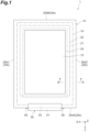
- FIG. 1 is a schematic plan view of a power storage module according to the present embodiment.
- the power storage module 1 is, for example, a power storage module used for a battery of one of various vehicles including a forklift, a hybrid vehicle, and an electric vehicle.
- the power storage module 1 is, for example, a secondary battery such as a nickel-metal hydride secondary battery or a lithium-ion secondary battery.
- the power storage module 1 may be an electric double-layer capacitor or an all-solid-state battery.
- the power storage module 1 is a lithium-ion secondary battery will be described.
- the power storage module 1 includes an electrode laminate 10 and an injected resin portion 50.
- the electrode laminate 10 has a rectangular shape when viewed in a Z-axis direction (first direction).
- the electrode laminate 10 has four outer side surfaces 20s.
- the injected resin portion 50 is bonded to an outer side surface 20sA (injection port surface) among the four outer side surfaces 20s.
- the outer side surface 20sB is a surface opposite the outer side surface 20sA.
- the outer side surface 20sC and the outer side surface 20sD are surfaces connecting the outer side surface 20sA and the outer side surface 20sB to each other.
- the power storage module may have a rectangular shape having a size of about 300 mm ⁇ 700 mm to 1300 mm ⁇ 2000 mm when viewed in the Z-axis direction.
- FIG. 2 is a cross-sectional view taken along line II-II in FIG. 1 , and illustrates the vicinity of the outer side surface 20sD. Note that, in the vicinity of the outer side surfaces 20sB and 20sC, too, cross sections similar to that in FIG. 2 are obtained.
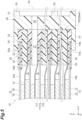
- FIG. 3 is a front view of the injected resin portion 50, and illustrates a part of the outer side surface 20sA.
- FIG. 4 is a cross section taken along line IV-IV in FIG. 3
- FIG. 5 is a cross section taken along line V-V in FIG. 3
- FIG. 6 is a cross section taken along line VI-VI in FIG. 3 .
- the electrode laminate 10 includes a plurality of electrodes stacked in the Z-axis direction.
- the Z-axis direction is a direction in which the electrodes are stacked and is a height direction of the power storage module 1.
- the plurality of electrodes includes a plurality of bipolar electrodes 11, a positive electrode terminal electrode 12, and a negative electrode terminal electrode 13.
- a separator 14 is interposed between electrodes adjacent to each other.
- Each bipolar electrode 11 includes a current collector 15, a positive electrode active material layer 16, and a negative electrode active material layer 17.
- the current collector 15 has a rectangular shape when viewed in the Z-axis direction, and has a sheet shape.
- the current collector 15 has a first region R1 in which active material layers (the positive electrode active material layer 16 and the negative electrode active material layer 17) are formed, and a frame-shaped second region R2 outside the first region R1.
- the first region R1 is provided at a center of the current collector 15 when viewed in the Z-axis direction.
- the positive electrode active material layer 16 is provided on a first surface 15a of the current collector 15.
- the negative electrode active material layer 17 is provided on a second surface 15b of the current collector 15.
- the plurality of bipolar electrodes 11 is stacked such that the positive electrode active material layer 16 of one bipolar electrode 11 and the negative electrode active material layer 17 of another bipolar electrode 11 adjacent to each other in the stacking direction face each other.
- the first surface 15a of the current collector 15 is a surface facing one side of the Z-axis direction
- the second surface 15b of the current collector 15 is a surface facing another side of the Z-axis direction.
- the positive electrode active material layer 16 and the negative electrode active material layer 17 each have a rectangular shape when viewed in the Z-axis direction.
- the negative electrode active material layer 17 is slightly larger than the positive electrode active material layer 16 when viewed in the Z-axis direction. In a plan view viewed from the Z-axis direction, an entire formation region of the positive electrode active material layer 16 is located in a formation region of the negative electrode active material layer 17.
- the positive electrode terminal electrode 12 includes a current collector 15 and a positive electrode active material layer 16 provided on a first surface 15a of the current collector 15.
- the positive electrode terminal electrode 12 does not include a positive electrode active material layer 16 or a negative electrode active material layer 17 on a second surface 15b of the current collector 15. That is, no active material layer is provided on the second surface 15b of the current collector 15 of the positive electrode terminal electrode 12.
- the positive electrode terminal electrode 12 is stacked on one of the bipolar electrodes 11 at an end of the electrode laminate 10 on the other side of the Z-axis direction.
- the positive electrode terminal electrode 12 is stacked on the bipolar electrode 11 such that the positive electrode active material layer 16 thereof faces the negative electrode active material layer 17 of the bipolar electrode 11.
- the negative electrode terminal electrode 13 includes a current collector 15 and a negative electrode active material layer 17 provided on a second surface 15b of the current collector 15.
- the negative electrode terminal electrode 13 does not include a positive electrode active material layer 16 or a negative electrode active material layer 17 on a first surface 15a of the current collector 15. That is, no active material layer is provided on the first surface 15a of the current collector 15 of the negative electrode terminal electrode 13.
- the negative electrode terminal electrode 13 is stacked on one of the bipolar electrodes 11 at an end of the electrode laminate 10 on the one side of the Z-axis direction.
- the negative electrode terminal electrode 13 is stacked on the bipolar electrode 11 such that the negative electrode active material layer 17 thereof faces the positive electrode active material layer 16 of the bipolar electrode 11.
- the separators 14 are disposed between adjacent bipolar electrodes 11, between the positive electrode terminal electrode 12 and the bipolar electrode 11, and between the negative electrode terminal electrode 13 and the bipolar electrode 11. Each separator 14 is interposed between the positive electrode active material layer 16 and the negative electrode active material layer 17, and isolates the positive electrode active material layer 16 and the negative electrode active material layer 17 from each other. Each separator 14 allows charge carriers such as lithium ions to pass while preventing a short circuit due to contact between adjacent electrodes.
- the current collector 15 is a chemically inactive electric conductor for continuously flowing a current through the positive electrode active material layer 16 and the negative electrode active material layer 17 during discharge or charge of the lithium-ion secondary battery.
- a material of the current collector 15 is, for example, a metal material, a conductive resin material, a conductive inorganic material, or the like.
- the conductive resin material include a resin obtained by adding a conductive filler to a conductive polymer material or a non-conductive polymer material as necessary.
- the current collector 15 may include a plurality of layers. In this case, each layer of the current collector 15 may contain the above-described metal material or conductive resin material.
- a covering layer may be formed on a surface of the current collector 15.
- the covering layer may be formed by a known method such as plating or spray coating.
- the current collector 15 may have, for example, a plate shape, a foil shape (for example, a metal foil), a film shape, a mesh shape, or the like.
- the metal foil include an aluminum foil, a copper foil, a nickel foil, a titanium foil, and a stainless steel foil.
- Examples of the stainless steel foil include SUS 304, SUS 316, and SUS 301 defined in JIS G 4305:2015.
- Mechanical strength of the current collector 15 can be secured by using a stainless steel foil as the current collector 15.
- the current collector 15 may be an alloy foil or a clad foil of the above-mentioned metal. When the current collector 15 has a foil shape, thickness of the current collector 15 may be, for example, 1 ⁇ m to 100 ⁇ m.
- the positive electrode active material layer 16 contains a positive electrode active material capable of occluding and releasing charge carriers such as lithium ions.
- the positive electrode active material include a lithium composite metal oxide having a stratified rock salt type structure, a metal oxide having a spinel structure, and a polyanionic compound.
- the positive electrode active material may be any material that can be used for the lithium-ion secondary battery.
- the positive electrode active material layer 16 may contain a plurality of the positive electrode active materials.
- the positive electrode active material layer 16 contains olivine lithium iron phosphate (LiFePO 4 ) as a composite oxide.
- the negative electrode active material layer 17 contains a negative electrode active material capable of occluding and releasing charge carriers such as lithium ions.
- the negative electrode active material may be any of a simple substance, an alloy, or a compound. Examples of the negative electrode active material include Li, carbon, and a metal compound.
- the negative electrode active material may be an element that can be alloyed with lithium, a compound thereof, or another material. Examples of the carbon include natural graphite, artificial graphite, hard carbon (non-graphitizing carbon), and soft carbon (graphitizing carbon). Examples of the artificial graphite include highly oriented graphite, and meso-carbon microbeads. Examples of the element that can be alloyed with lithium include silicon, and tin.
- the negative electrode active material layer 17 contains graphite as a carbon-based material.
- Each of the positive electrode active material layer 16 and the negative electrode active material layer 17 may further contain a conductive aid, a binder, an electrolyte (polymer matrix, ion conductive polymer, electrolytic solution, or another electrolyte) for enhancing electric conductivity, a supporting electrolyte salt (lithium salt) for enhancing ion conductivity, and other components as necessary.
- the conductive aid is added to enhance the conductivity of each electrode (the bipolar electrodes 11, the positive electrode terminal electrode 12, and the negative electrode terminal electrode 13).
- the conductive aid is, for example, acetylene black, carbon black, graphite, or another material.
- binder examples include fluorine-containing resins such as polyvinylidene fluoride, polytetrafluoroethylene, and fluororubber, thermoplastic resins such as polypropylene and polyethylene, imide resins such as polyimide and polyamideimide, alkoxysilyl group-containing resins, acrylic resins such as acrylic acid and methacrylic acid, alginates such as styrene-butadiene rubber (SBR), carboxymethyl cellulose, sodium alginate, and ammonium alginate, water-soluble cellulose ester crosslinked bodies, and starch-acrylic acid graft polymers.
- binders can be used alone or in combination. For example, water, N-methyl-2 pyrrolidone (NMP), or the like is used as a solvent.
- the separators 14 may each be, for example, a porous sheet or a nonwoven fabric containing a polymer that absorbs and holds an electrolyte.
- a material of the separators 14 include polypropylene, polyethylene, polyolefin, and polyester.
- the separators 14 may each have a single layer structure or a multilayer structure.
- the multilayer structure may include, for example, a ceramic layer or another layer as an adhesive layer or a heat resistant layer.
- the separators 14 may be impregnated with an electrolyte.
- the separators 14 may include an electrolyte such as a polymer electrolyte or an inorganic electrolyte.
- Examples of the electrolyte with which the separator 14 is impregnated include a liquid electrolyte (electrolytic solution) containing a nonaqueous solvent and an electrolyte salt dissolved in the nonaqueous solvent, or a polymer gel electrolyte containing an electrolyte held in a polymer matrix.
- a liquid electrolyte electrolytic solution
- electrolyte salt dissolved in the nonaqueous solvent
- polymer gel electrolyte containing an electrolyte held in a polymer matrix.
- a known lithium salt such as LiClO 4 , LiAsF 6 , LiPF 6 , LiBF 4 , LiCF 3 SO 3 , LiN(FSO 2 ) 2 , or LiN(CF 3 SO 2 ) 2 may be used as an electrolyte salt.
- a known solvent such as a cyclic carbonate, a cyclic ester, a chain carbonate, a chain ester, or an ether may be used as the nonaqueous solvent. Note that two or more of these known solvent materials may be used in combination.
- the electrode laminate 10 further includes a sealing body 20.
- the sealing body 20 is formed in a frame shape in a peripheral edge portion of the electrode laminate 10 in such a way as to form an outer edge of the electrode laminate 10 when viewed in the Z-axis direction.
- the sealing body 20 can be bonded to the first surface 15a and the second surface 15b of the current collectors 15 at peripheral edge portions 15c of the current collectors 15.
- the sealing body 20 forms internal spaces S between the current collectors 15 adjacent to each other in the Z-axis direction, and seals each of the internal spaces S.
- An electrolytic solution (not illustrated) is contained in each internal space S. That is, the sealing body 20 defines the internal spaces S containing the electrolytic solution in cooperation with the current collectors 15 adjacent to each other in the Z-axis direction.
- the sealing body 20 blocks permeation of the electrolytic solution to the outside.
- the sealing body 20 suppresses intrusion of moisture and the like from the outside of the electrode laminate 10 into the internal spaces S.
- the sealing body 20 prevents gas generated at each electrode due to, for example, charge and discharge reactions or the like from leaking to the outside of the power storage module 1. Edge portions of the separators 14 are bonded to the sealing body 20.
- the sealing body 20 contains an insulating material. Examples of a material of the sealing body 20 include various resin materials such as polypropylene, polyethylene, polystyrene, ABS resin, acid-modified polypropylene, acid-modified polyethylene, and acrylonitrile styrene resin.
- An example of the sealing body 20 includes a plurality of sealing materials 21, a pair of end sealing materials 24, and a plurality of spacers 22.
- the sealing materials 21, the end sealing materials 24, and the spacers 22 may be frame-shaped members formed in sheet shapes.
- a welded end 23 is formed in the sealing body 20.
- the plurality of sealing materials 21 is provided in the second region R2 of the current collectors 15 constituting the plurality of bipolar electrodes 11.
- the sealing materials 21 have a frame shape when viewed in the Z-axis direction.
- the sealing materials 21 are provided along the peripheral edge portions 15c of the current collectors 15.
- the peripheral edge portions 15c are outer peripheral portions of the second region R2.
- the sealing materials 21 are provided in such a way as to reach the second surfaces 15b from the first surfaces 15a of the current collectors 15 through end surfaces, and cover the peripheral edge portions 15c.
- the sealing materials 21 can be welded to at least the first surfaces 15a or the second surfaces 15b of the current collectors 15.
- the end sealing material 24 is provided in the second region R2 of the current collector 15 constituting the positive electrode terminal electrode 12 and the negative electrode terminal electrode 13.
- the end sealing materials 24 have frame shapes when viewed in the Z-axis direction.
- the end sealing materials 24 are provided along the peripheral edge portions 15c of the current collectors 15. For example, when viewed in the Z direction, width of the sealing materials 21 in a region along the outer side surface 20sA is greater than width of the sealing materials 21 in regions along the outer side surfaces 20sB, 20sC, and 20sD.
- width of the end sealing materials 24 is greater than that of the sealing materials 21. That is, inner edges of the end sealing materials 24 are located inside inner edges of the sealing materials 21.
- the width of the sealing materials 21 in the regions along the outer side surfaces 20sA and 20sB may be distances of the sealing materials 21 in the regions in the Y-axis direction (second direction).
- the width of the sealing materials 21 in the regions along the outer side surfaces 20sC and 20sD may be distances of the sealing materials 21 in the regions in an X-axis direction (third direction).
- the spacers 22 have frame shapes when viewed in the Z-axis direction.
- the spacers 22 are disposed along the peripheral edge portions 15c of the current collectors 15.
- the spacers 22 are disposed in such a way as to be interposed between the sealing materials 21 adjacent to each other in the Z-axis direction.
- the spacers 22 can be welded to at least one of the sealing materials 21 adjacent to each other in the Z-axis direction.
- the spacers 22 are disposed in such a way as to be interposed between the sealing materials 21 and the end sealing materials 24 adjacent to each other in the Z-axis direction.
- the spacers 22 can be welded to at least the sealing materials 21 and the end sealing materials 24 adjacent to each other in the Z-axis direction.
- the spacers 22 can hold spaces between the current collectors 15 adjacent to each other in the Z-axis direction. That is, the spacers 22, the sealing materials 21, and the end sealing materials 24 define the internal spaces S between the adjacent current collectors 15.
- width of the spacers 22 in the region along the outer side surface 20sA is greater than that of the spacers 22 in the regions along the outer side surfaces 20sB, 20sC, and 20sD.
- the width of the spacers 22 is smaller than that of the sealing materials 21. That is, in the regions along the outer side surfaces 20sB, 20sC, and 20sD, inner edges of the spacers 22 are located outside the inner edges of the sealing materials 21.
- the width of the spacers 22 is greater than that of the sealing materials 21. That is, in the region along the outer side surface 20sA, the inner edges of the spacers 22 are located inside the inner edges of the sealing materials 21. Note that the inner edges of the spacers 22 are located outside the inner edges of the end sealing materials 24 in any region.
- the welded end 23 is formed by welding and integrating ends of the plurality of sealing materials 21, the pair of end sealing materials 24, and the plurality of spacers 22 on a side opposite the internal spaces S.
- the welded end 23 surrounds the current collectors 15 when viewed in the Z-axis direction, and has a frame shape in such a way as to form an outer periphery of the electrode laminate 10.
- a surface of the welded end 23 on the surface side opposite the internal spaces S extends in the Z-axis direction and constitutes the outer side surface 20s of the sealing body 20.
- the sealing body 20 includes the outer side surface 20s opposite the internal spaces S.
- the outer side surface 20s may be formed as a flat surface.
- the sealing body 20 has a plurality of communication holes 27 communicating with the plurality of internal spaces S (see FIG. 5 ).
- the communication holes 27 are cutout portions formed in the spacers 22.
- the communication holes 27 penetrate the welded end 23.
- the communication holes 27 each have an opening in the corresponding internal space S and another opening in the outer side surface 20s of the sealing body 20. In the illustrated example, an opening is formed in the outer side surface 20sA.
- the injected resin portion 50 is a reinforcing member that reinforces the outer side surface 20sA in which the communication holes 27 are formed.
- the injected resin portion 50 is molded in a predetermined shape to provide injection ports communicating with the communication holes 27.
- the injected resin portion 50 is bonded to the sealing body 20.
- the injected resin portion 50 is integrally bonded to the sealing body 20 through injection molding.
- An example of the injected resin portion 50 includes a main body portion 51, a first overhang portion 55, a second overhang portion 57, and first thin portions 59.
- the main body portion 51 partially covers the outer side surface 20sA.
- the main body portion 51 covers the outer side surface 20sA in such a way as to include a region (main body region) R3 in which the plurality of communication holes 27 formed in the outer side surface 20sA is formed.
- the plurality of communication holes 27 communicates with the plurality of internal spaces S, respectively.
- 30 communication holes 27 corresponding to 30 internal spaces formed between the current collectors 15 are discretely arranged in the X-axis direction and the Z-axis direction.
- communication holes 27 corresponding to internal spaces of first to tenth layers from a positive electrode terminal electrode 12 side are discretely arranged at equal intervals in the X-axis direction, and communication holes 27 corresponding to internal spaces of eleventh to twentieth layers and communication holes 27 corresponding to internal spaces of twenty-first to thirtieth layers are arranged in order in the Z-axis direction below the internal spaces of the first to tenth layers.
- the main body portion 51 extends in a rectangular shape along the X-axis direction and the Z-axis direction to cover the main body region R3 where the 30 communication holes 27 are formed.
- the main body portion 51 is formed in a rectangular plate shape having a predetermined thickness in the Y-axis direction.
- a thickness L2 of the main body portion 51 in the Y-axis direction may be 2.0 ⁇ 0.5 mm.
- the main body portion 51 has openings 52 at positions corresponding to the communication holes 27.
- the thickness L2 of the main body portion 51 corresponds to depth, in the Y-axis direction, of the openings 52 provided in the main body portion 51.
- the main body portion 51 includes frame-shaped protruding frame portions 53 that protrude outward in the Y-axis direction.
- the protruding frame portions 53 surround the corresponding openings 52 when viewed in the Y-axis direction (see FIG.
- protruding frame portions 53 in which three spaces for separating three vertically arranged openings 52 from one another are formed are arranged in the X-axis direction.
- thickness of the protruding frame portions 53 in the Y-axis direction may be about 0.5 mm to 6.0 mm.
- each protruding frame portions 53 is used when an electrolyte solution is injected into the corresponding internal space S.
- the electrolyte solution for example, a nozzle of a solution injection device is brought into close contact with a top surface of the protruding frame portion 53, and the electrolyte solution is introduced into the space of the protruding frame portion 53 from the nozzle.
- the electrolyte solution can thus be injected into the internal spaces S through the openings 52 and the communication holes 27.
- a laminate sheet 54 for sealing the protruding frame portions 53 is provided for the protruding frame portions 53 (see FIG. 5 ).
- the laminate sheet 54 may be, for example, a sheet obtained by covering a metal layer composed of aluminum or the like with a resin layer.
- the laminate sheet 54 may be fused to, for example, the top surfaces of the protruding frame portions 53.
- both end surfaces of the electrode laminate 10 in the Z-axis direction are a first end surface 10a and a second end surface 10b.
- the first end surface 10a is an outermost surface of the electrode laminate 10 on a positive side of the Z-axis direction. That is, the first end surface 10a includes an exposed surface of the second surface 15b of the positive electrode terminal electrode 12 and an exposed surface of the end sealing material 24 bonded to a peripheral edge of the positive electrode terminal electrode 12.
- the second end surface 10b is an outermost surface of the electrode laminate 10 on a negative side of the Z-axis direction.
- the second end surface 10b includes an exposed surface of the first surface 15a of the negative electrode terminal electrode 13 and an exposed surface of the end sealing material 24 bonded to a peripheral edge of the negative electrode terminal electrode 13.
- the first overhang portion 55 is formed in such a way as to be connected to a first end edge 51a of the main body portion 51 in the Z-axis direction.
- the first overhang portion 55 partially covers the first end surface 10a of the electrode laminate 10.
- the first overhang portion 55 partially covers the end sealing material 24 bonded to the positive electrode terminal electrode 12 constituting the first end surface 10a.
- an end edge 55a of the first overhang portion 55 extends to a position inside outer edges 14a of the separators 14 and outside inner edges 22a of the spacers 22 when viewed in the Z-axis direction.
- the first overhang portion 55 may be formed in a rectangular plate shape having the same length as the main body portion 51 in the X-axis direction.
- thickness of the first overhang portion 55 in the Z-axis direction may be 1.5 ⁇ 0.5 mm or may be thinner.
- the second overhang portion 57 is connected to a second end edge 51b of the main body portion 51 on a side opposite the first end edge 51a to partially cover the second end surface 10b of the electrode laminate 10.
- the second overhang portion 57 partially covers the end sealing material 24 bonded to the negative electrode terminal electrode 13 constituting the second end surface 10b.
- an end edge 57a of the second overhang portion 57 extends to a position inside the outer edges 14a of the separators 14 and outside the inner edges 22a of the spacers 22 when viewed in the Z-axis direction.
- the second overhang portion 57 may be formed in a rectangular plate shape having the same length as the main body portion 51 in the X-axis direction.
- thickness of the second overhang portion 57 in the Z-axis direction may be 1.5 ⁇ 0.5 mm, and may be different from the thickness of the first overhang portion 55.
- the first thin portions 59 are formed in such a way as to be connected to a third end edge 51c and a fourth end edge 51d, which are two end edges of the main body portion 51 in the X-axis direction (see FIG. 3 ).
- the first thin portions 59 extend from the main body portion 51 along the outer side surface 20sA and are bonded to the outer side surface 20sA. Size of the first thin portions 59 in the Z-axis direction may be equal to that of the main body portion 51 in the Z-axis direction.
- a thickness L1 (see FIG. 6 ) of the first thin portions 59 in the Y-axis direction is smaller than the thickness L2 (see FIG. 4 ) of the main body portion 51 in the Y-axis direction.
- the thickness L1 of the first thin portions 59 may be 1/3 or less of the thickness L2 of the main body portion 51, instead.
- the thickness of the first thin portions 59 in the Y-axis direction may be 0.5 mm or less. Note that, in the example of FIG. 3 , the first thin portions 59 have rectangular shapes when viewed in the Y-axis direction, but the first thin portions 59 only need to have regions bonded to the outer side surface 20sA, and the shapes of the first thin portions 59 are not limited to rectangular shapes.
- conductive members that function as terminals for extracting currents from the power storage module 1 may be disposed and electrically connected.
- the conductive members can be used to electrically connect a plurality of power storage modules 1 to one another.
- the conductive members can also be used as restraining members in order to apply restraining loads to the electrode laminate 10.
- cooling channels may be formed in the conductive members. The electrode laminate 10 can be cooled by circulating a cooling medium through the cooling channels formed in the conductive members.
- FIG. 7 is a flowchart illustrating an example of a method for manufacturing the power storage module.
- an electrode laminate 10 including a plurality of electrodes stacked in the Z-axis direction is formed (step S1).
- the electrode laminate 10 is thus prepared.
- the sealing body 20 of the formed electrode laminate 10 does not include the welded end 23. That is, the end sealing materials 24, the sealing materials 21, and the spacers 22 stacked in the Z-axis direction are not welded to each other.
- the spacers 22 may have include cutout portions connected from the internal spaces S to the outer edge at positions corresponding to the communication holes 27.
- step S1 the electrode laminate 10 is formed in a state where inserts are disposed in the cutout portions formed in the spacers 22.
- the electrode laminate 10 formed in this manner includes a plurality of inserts protruding from a side surface corresponding to the outer side surface 20sA. The inserts are inserted into the cutout portions to prevent the cutout portions from being blocked in subsequent steps. By removing the inserts after the injection molding, the communication holes 27 and the openings 52 are formed in portions where the inserts are disposed.
- the inserts may be, for example, metal plates.
- the welded end 23 is formed on the electrode laminate 10 (step S2).
- the internal spaces S are formed between adjacent current collectors 15.
- outer edge portions of the sealing materials 21, the end sealing materials 24, and the spacers 22, which constitute the electrode laminate 10, on a side opposite the internal spaces S are welded to each other.
- the welded end 23 is formed in a state where the inserts are disposed in the cutout portions of the spacers 22.
- thickness of the welded end 23 corresponding to the other outer side surfaces 20sB, 20sC, and 20sD may be greater than that of the welded end 23 corresponding to the outer side surface 20sA.
- the step of forming the injected resin portion 50 includes a step of attaching a mold partially covering the outer side surface 20sA to the electrode laminate 10 and a step of injecting a resin into a molding space of the mold.
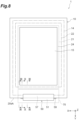
- FIG. 8 is a plan view illustrating a position of a mold 70 attached to the example of the power storage module. In FIG. 8 , an attachment position of the mold 70 is indicated by a broken line.
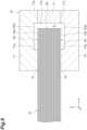
- FIG. 9 is a cross-sectional view schematically illustrating the mold taken along line IX-IX in FIG. 8 .
- FIG. 10 is a cross-sectional view schematically illustrating the mold taken along line X-X in FIG. 8 .
- FIG. 11 is a cross-sectional view schematically illustrating the mold taken along line XI-XI in FIG. 8 .
- step S3 the mold 70 is attached to the electrode laminate 10 placed on a placement table, so that a continuous molding space C is formed between the main body region R3, a first overhang region R4, and a second overhang region R5 of the electrode laminate 10 (see FIG. 9 ).
- Thickness of the molding space C in the Y-axis direction corresponds to the thickness L2 (see FIG. 4 ) of the main body portion 51.
- the thickness of the molding space C in the Z-axis direction may be controlled in such a way as to be constant. Accordingly, the power storage module 1 can be accurately and stably manufactured.
- the main body region R3 is a region including the plurality of communication holes 27 in the outer side surface 20sA.
- the main body region R3 is a bonding surface with the main body portion 51.
- the first overhang region R4 is connected to a first end edge R3a of the main body region R3 in the Z-axis direction.
- the first overhang region R4 is a region partially extending to the first end surface 10a intersecting the Z-axis direction in the electrode laminate 10.
- the first overhang region R4 is a bonding surface with the first overhang portion 55.
- the second overhang region R5 is connected to a second end edge R3b opposite the first end edge R3a in the main body region R3.
- the second overhang region R5 is a region partially extending to the second end surface 10b opposite the first end surface 10a in the electrode laminate 10.
- the second overhang region R5 is a bonding surface with the second overhang portion 57.
- a first thin space SS1 extending from the molding space C along the outer side surface 20sA is formed (see FIG. 10 ). Thickness of the first thin space SS1 in the Y-axis direction corresponds to the thickness L1 (see FIG. 4 ) of the first thin portions 59. Note that since the first thin space SS1 is a space formed in the mold 70 together with the molding space C, the first thin space SS1 can be regarded as a part of the molding space C, but in the present specification, the first thin space SS1 is defined as another space connected to the molding space C.
- the mold 70 may include a first mold 71 and a second mold 74 that sandwich the electrode laminate 10 in the Z-axis direction.
- the mold 70 may include a third mold 77 disposed between the first mold 71 and the second mold 74.
- the first mold 71 has a contact surface 72 in contact with the first end surface 10a of the electrode laminate 10 and an inner surface 71a facing the first overhang region R4.
- the second mold 74 has a contact surface 75 in contact with the second end surface 10b of the electrode laminate 10 and an inner surface 74a facing the second overhang region R5.
- the electrode laminate 10 is sandwiched between the contact surface 72 of the first mold 71 and the contact surface 75 of the second mold 74 such that the outer edge of the electrode laminate 10 is exposed in the molding space C.
- the contact surface 72 of the first mold 71 may contact the end sealing material 24 at a position where the spacer 22, the sealing material 21, and the separator 14 overlap when viewed in the Z-axis direction.
- the contact surface 75 of the second mold 74 may contact the end sealing material 24 at a position where the spacer 22, the sealing material 21, and the separator 14 overlap.
- the current collector 15 may extend at the position where the spacer 22, the sealing material 21, and the separator 14 overlap.
- the third mold 77 is disposed between the first mold 71 and the second mold 74 in the Z-axis direction, and forms the molding space C together with the first mold 71 and the second mold 74.
- the third mold 77 has a contact surface 77b in contact with the first mold 71, a contact surface 77c in contact with the second mold 74, and an inner surface 77a facing the main body region R3.
- the inner surface 77a of the third mold 77 is separated from the main body region R3 of the outer side surface 20sA by a distance corresponding to the thickness L2 (see FIG. 4 ) of the main body portion 51.
- the second mold 74 is disposed in such a way as to be in contact with the electrode laminate 10.
- the electrode laminate 10 may be placed on the placement table such that an end including the outer side surface 20sA protrudes from the placement table.
- the first mold 71 presses the electrode laminate 10 in the Z-axis direction, and the electrode laminate 10 is sandwiched between the first mold 71 and the second mold 74.
- the third mold 77 is disposed.
- the mold 70 only needs to partially cover the outer side surface 20sA of the electrode laminate 10. In an example, both end edges of the outer side surface 20sA in the X-axis direction may be exposed to the outside of the mold 70.
- the contact surface 72 of the first mold 71 and the contact surface 75 of the second mold 74 extend to positions of the outer side surface 20sA, which is a part of the outer periphery of the electrode laminate 10.
- the third mold 77 has an inner surface 77d closer to the outer side surface 20sA of the electrode laminate 10 than the inner surface 77a is.
- the inner surface 77d faces first thin regions R6 in which the first thin portions 59 are bonded to the outer side surface 20sA.
- a distance from the inner surface 77d to the outer side surface 20sA corresponds to the thickness L1 (see FIG. 6 ) of the first thin portions 59.
- the contact surfaces of the first mold 71 and the second mold 74 extend to positions of the outer side surface 20sA of the electrode laminate 10 as in the ranges where the first thin portions 59 are formed.
- the third mold 77 has a contact surface 77e in contact with the outer side surface 20sA. In a state where the mold 70 is attached to the electrode laminate 10, the contact surface 77e of the third mold 77 may be pressed against the outer side surface 20sA of the electrode laminate 10.
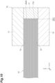
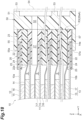
- FIG. 12 is a diagram schematically illustrating a contact surface of a mold with respect to an electrode laminate.
- the contact surface 72 of the first mold 71 and the contact surface 75 of the second mold 74 have the same shape.
- FIG. 12 representatively illustrates the contact surface 72 of the first mold 71.
- grooves are formed in the contact surface 72 of the first mold 71.
- the grooves in the illustrated example form a mesh pattern when viewed in the Z-axis direction. That is, the grooves are formed such that a plurality of first straight lines 72a inclined at a first angle and a plurality of second straight lines 72b inclined at a second angle intersect each other when viewed in the Z-axis direction.
- Both the first straight lines 72a and the second straight lines 72b intersect both the X-axis direction and the Y-axis direction.
- surface roughness of the contact surfaces of the first mold 71 and the second mold 74 is greater than that of the surfaces of the mold 70 forming the molding space C (that is, the inner surfaces). Note that both ends of the contact surface 72 in the Y-axis direction may be subjected to R processing.
- step S4 a resin is injected into the molding space C of the mold 70 to mold the injected resin portion 50 (step S4).
- the molding space C can be filled with the resin
- the first thin space SS1 can be filled with the resin leaking from the molding space C. It is not always necessary in step S4 that the first thin space SS1 is completely filled with the resin, and it is sufficient that a part of the first thin space SS1 is filled with the resin. That is, the first thin portions 59 formed in step S4 need not have rectangular shapes corresponding to the first thin space SS1 when viewed in the Y-axis direction, and may have chips at ends or peripheral edges.
- FIGS. 9 to 11 schematically illustrate the mold 70, but the mold 70 may be provided with recesses or the like corresponding to the protruding frame portions 53.
- a holding portion that holds the inserts protruding from the electrode laminate 10 may be formed in the mold 70.
- FIG. 13 is a schematic plan view of another example of the power storage module.
- FIG. 14 is a schematic cross-sectional view of the power storage module illustrated in FIG. 13 .
- FIG. 15 is a schematic cross-sectional view of a mold illustrated in FIG. 13 .
- the power storage module includes an injected resin portion 150 having a shape different from that of the injected resin portion 50.
- the injected resin portion 150 includes a main body portion 51, a first overhang portion 55, a second overhang portion 57, first thin portions 59, and second thin portions 159. Configuration of the main body portion 51, the first overhang portion 55, the second overhang portion 57, and the first thin portions 59 is the same as in the injected resin portion 50, and description thereof is omitted.
- the second thin portions 159 are formed in such a way as to be connected to both end edges of the first overhang portion 55 and the second overhang portion 57 in the X-axis direction. In addition, the second thin portions 159 may be connected to the first thin portions 59. The second thin portions 159 extend from the first overhang portion 55 and the second overhang portion 57 along the end sealing materials 24.
- a thickness L3 of the second thin portion 159 in the Z-axis direction is smaller than thicknesses L4 and L5 of the first overhang portion 55 and the second overhang portion 57 in the Z-axis direction. For example, the thickness L3 may be smaller than or equal to 1/3 of the thickness L4 or L5.
- the second thin portions 159 and the first thin portions 59 may have the same thickness, and a relationship between the thickness L3 of the second thin portions 159 and the thicknesses L4 and L5 of the first overhang portion 55 and the second overhang portion 57 may be the same as a relationship between the thickness L1 of the first thin portions 59 and the thickness L2 of the main body portion 51.
- the second thin portion 159 has a rectangular shape when viewed in the Z-axis direction, but the shape of the second thin portion 159 is not limited to a rectangular shape.
- FIG. 15 which is a cross-sectional view of a mold 170 at a position corresponding to the second thin portions 159
- the first thin space SS1 and a second thin space SS2 for forming the first thin portions 59 and the second thin portions 159 are formed by a first mold 171, a second mold 174, and a third mold 177 constituting the mold 170.
- the first mold 171 has a contact surface 172 in contact with the first end surface 10a (end sealing material 24) of the electrode laminate 10, and an inner surface 171a that faces a second thin region R7, which is a region where the second thin portion 159 is bonded to the first end surface 10a.
- the second mold 174 has a contact surface 175 in contact with the second end surface 10b (end sealing material 24) of the electrode laminate 10, and an inner surface 174a that faces a second thin region R7, which is a region where the second thin portion 159 is bonded to the second end surface 10b.
- the inner surface 171a of the first mold 171 and the inner surface 174a of the second mold 174 are separated from the electrode laminate 10 by a distance corresponding to the second thin portions 159.
- FIG. 16 is a schematic plan view of yet another example of a power storage module.
- FIG. 17 is a schematic cross-sectional view of a mold illustrated in FIG. 16 .
- the power storage module includes an injected resin portion 250 having a shape different from that of the injected resin portion 150.
- the injected resin portion 250 includes a main body portion 51, a first overhang portion 55, a second overhang portion 57, first thin portions 59, second thin portions 159, and a third thin portion 259. Configuration of the main body portion 51, the first overhang portion 55, the second overhang portion 57, the first thin portions 59, and the second thin portions 159 is the same as in the injected resin portion 150, and description thereof is omitted.
- the third thin portion 259 is formed in such a way as to be connected to the end edges of the first overhang portion 55 and the second overhang portion 57 in the Y-axis direction.
- the third thin portion 259 may be connected to the second thin portions 159.
- the third thin portion 259 extends from the first overhang portion 55 and the second overhang portion 57 along the end sealing materials 24. Thickness of the third thin portion 259 in the Z-axis direction may be smaller than that of the first overhang portion 55 and the second overhang portion 57 in the Z-axis direction, and, for example, may be the same as that of the second thin portions 159.
- the third thin portion 259 has a rectangular shape when viewed in the Z-axis direction, but the shape of the third thin portion 259 is not limited to a rectangular shape.
- a first mold 271 has, in a range in the X-axis direction where the third thin portion 259 is formed, a contact surface 272 in contact with the first end surface 10a (end sealing material 24) of the electrode laminate 10, an inner surface 271a facing a third thin region R8, which is a region where the third thin portion 259 is bonded to the first end surface 10a, and an inner surface 271b facing the first overhang region R4.
- a second mold 274 has a contact surface 275 in contact with the second end surface 10b (end sealing material 24) of the electrode laminate 10, an inner surface 274a facing a third thin region R8, which is a region where the third thin portion 259 is bonded to the first end surface 10a, and an inner surface 274b facing the second overhang region R5.
- the inner surface 271a of the first mold 271 and the inner surface 274a of the second mold 274 are separated from the electrode laminate 10 (end sealing materials 24) by a distance corresponding to the third thin portion 259.
- the third mold 277 has a contact surface 277b in contact with the first mold 271, a contact surface 277c in contact with the second mold 274, and an inner surface 277a facing the main body region R3.
- the resin in the molding space C of the mold 270 flows into a first thin space SS1, a second thin space SS2, and a third thin space SS3.
- the first thin portions 59, the second thin portions 159, and the third thin portion 259 are formed.
- FIG. 18 is a schematic cross-sectional view of yet another example of a power storage module.
- the power storage module includes the injected resin portion 50 as in the example of FIG. 5 , but the power storage module may include the injected resin portion 150 or the injected resin portion 250, instead.
- laminate sheets 25 may be bonded to the end sealing materials 24 constituting the first end surface 10a and the second end surface 10b of the electrode laminate 10.
- the laminate sheets 25 may be welded to the end sealing materials 24.
- the laminate sheets 25 may each be a sheet obtained by covering a metal layer composed of aluminum or the like with a resin layer.
- the end sealing materials 24 may be covered with the laminate sheets 25.
- a surface of the end sealing material 24 bonded to the positive electrode terminal electrode 12 along the first end surface 10a and a surface of the end sealing material 24 bonded to the negative electrode terminal electrode 13 along the second end surface 10b are covered with the laminate sheets 25.
- shapes of the laminate sheets 25 match the shapes of the end sealing materials 24.
- the laminate sheets 25 may be bonded to the end sealing materials 24 at any stage before step S3 described above. By bonding the laminate sheets 25 to outer side surfaces of the end sealing materials 24, rigidity of the electrode laminate 10 is improved. As a result, in step S3, for example, the mold can be more stably attached to the electrode laminate 10.
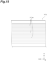
- FIG. 19 is a diagram illustrating another example of the contact surface of the mold with respect to the electrode laminate. Grooves are formed in a contact surface 372 of the mold illustrated in FIG. 19 . A plurality of grooves 372a extending in the X-axis direction when viewed in the Z-axis direction is formed in the contact surface 372 in the illustrated example. The grooves 372a are arranged at equal intervals in the Y-axis direction.
- an example of the power storage module 1 includes the electrode laminate 10 including the plurality of electrodes (the bipolar electrodes 11, the positive electrode terminal electrode 12, and the negative electrode terminal electrode 13) stacked in the first direction, the electrode laminate 10 including the sealing body 20 provided in such a way as to form the internal spaces S between the adjacent electrodes and seal the internal spaces S, and the injected resin portion 50 bonded to the sealing body 20.
- the plurality of electrodes includes the plurality of current collectors 15 having rectangular shapes when viewed in the Z-axis direction.
- the sealing body 20 includes the welded end 23 in which the outer peripheral edges of the plurality of frame-shaped members (the sealing materials 21 and the spacers 22) stacked in the Z-axis direction are welded to each other while being interposed between the plurality of current collectors 15.
- the sealing body 20 includes the first end surface 10a and the second end surface 10b, which are both end surfaces of the electrode laminate 10 in the Z-axis direction, the outer side surface 20sA, which is one of the four outer side surfaces 20s constituting a circumferential surface (a surface defining an outer edge when viewed in the Z-axis direction) of the welded end 23 and to which the injected resin portion 50 is bonded, and the plurality of communication holes 27 through which an outside of the outer side surface 20sA communicates with each of the plurality of internal spaces S.
- the injected resin portion 50 includes the main body portion 51 having the plurality of openings 52 connected to the plurality of communication holes 27, the main body portion 51 partially covering the outer side surface 20sA, the first overhang portion 55 connected to the main body portion 51 and partially covering the first end surface 10a, and the second overhang portion 57 connected to the main body portion 51 and partially covering the second end surface 10b.
- the main body portion 51 includes the plurality of protruding frame portions 53 protruding in the Y-axis direction intersecting the outer side surface 20sA.
- the plurality of protruding frame portions 53 surround the openings 52 connected to the plurality of communication holes 27 when viewed in the Y-axis direction.
- the communication holes 27 penetrating to the internal spaces S are provided at the welded end 23 of the sealing body 20 formed at the outer peripheral edge of the electrode laminate 10.
- the injected resin portion 50 including the protruding frame portions 53 surrounding the communication holes 27 is bonded to the sealing body 20.
- the injected resin portion 50 includes the main body portion 51 covering the outer side surface 20sA on which the welded end 23 is formed, the first overhang portion 55 extending from the main body portion 51 to the first end surface 10a of the electrode laminate 10, and the second overhang portion 57 extending from the main body portion 51 to the second end surface 10b of the electrode laminate 10.
- the injected resin portion 50 is provided for only one of the four outer side surfaces, an increase in size of the power storage module 1 is suppressed.
- Such an injected resin portion 50 does not require a mold large enough to surround an entire periphery of the electrode laminate 10, and can be formed by a mold only large enough to partially cover the outer side surface 20sA of the electrode laminate 10. It is therefore possible to suppress an increase in size of the mold required for the manufacture.
- the injected resin portion 50 can be firmly bonded to the sealing body 20, and moisture permeation and gas permeation in the Z-axis direction between the internal spaces S and the outside are suppressed.
- the outer side surfaces 20s of the electrode laminate 10 are formed by welding the sealing materials 21, the end sealing materials 24, and the spacers 22.
- the outer side surfaces 20s therefore, are not necessarily flat surfaces, and might be constituted by end surfaces having unevenness. When the outer side surfaces 20s have unevenness, it is possible that bonding power between the outer side surfaces 20s and the injected resin portion 50 is deteriorated.
- An example of the injected resin portion 50 may include the first thin portion 59 connected to the main body portion 51 and bonded to the outer side surface 20sA from the main body portion 51 along the outer side surface 20sA, and thickness of the first thin portion 59 in the Y-axis direction may be smaller than thickness of the main body portion 51 in the Y-axis direction. With this configuration, the injected resin portion 50 can be more firmly bonded to the sealing body 20 formed on the outer peripheral edge of the electrode laminate 10.
- An example of the injected resin portion 150 may include the second thin portion 159 connected to the first overhang portion 55 and bonded to the first end surface 10a from the first overhang portion 55 along the first end surface 10a, and thickness of the second thin portion 159 in the Z-axis direction may be smaller than thickness of the first overhang portion 55 in the Z-axis direction.
- an example of the injected resin portion 250 may include the third thin portion 259 connected to the first overhang portion 55 and bonded to the first end surface 10a from the first overhang portion 55 along the first end surface 10a, and thickness of the third thin portion 259 in the Z-axis direction may be smaller than thickness of the first overhang portion 55 in the Z-axis direction. With this configuration, the injected resin portion 150 or 250 can be more firmly bonded to the sealing body 20 formed on the outer peripheral edge of the electrode laminate 10. Note that thickness of the second thin portion 159 and the third thin portion 259 may be the same or different from each other.
- the current collectors 15 includes the first region R1 provided at a center of the current collectors 15 when viewed from the Z-axis direction and provided with active material layers, and the frame-shaped second region R2 outside the first region R1.
- the electrode laminate 10 may include the plurality of frame-shaped sealing materials 21 provided in the second region R2 of the plurality of current collectors 15, and the plurality of spacers 22 interposed between the sealing materials 21 adjacent to each other in the Z-axis direction and defining, together with the plurality of sealing materials 21, the internal spaces S between the current collectors 15. With this configuration, the outer peripheral edges of the sealing materials 21 and the outer peripheral edges of the spacers 22 are welded to each other to form the welded end 23.
- an example of the method for manufacturing the power storage module 1 includes the steps of preparing the electrode laminate 10 including the plurality of electrodes stacked in the Z-axis direction and having both end surfaces in the Z-axis direction as the first end surface 10a and the second end surface 10b (step S1), providing the welded end 23 on the electrode laminate 10 such that internal spaces S are formed between the adjacent electrodes (step S2), and forming the injected resin portion 50 at the welded end 23 (step S3).
- the step of providing the welded end 23 includes the step of welding the outer peripheral edges of the plurality of sealing materials 21, the plurality of spacers 22, and the end sealing materials 24 to one another.
- the step of forming the injected resin portion 50 includes the steps of attaching the mold 70 to the electrode laminate 10 in such a way as to form the continuous molding space C between, in the outer side surface 20sA, the main body region R3 including the plurality of communication holes 27, the first overhang region R4 connected to the main body region R3 and partially extending on the first end surface 10a, and the second overhang region R5 connected to the main body region R3 and partially extending on the second end surface 10b, and forming the injected resin portion 50 by injecting a resin into the molding space C attached to the electrode laminate 10.
- the injected resin portion 50 can be formed by the mold 70 only large enough to partially cover the outer side surface 20sA of the electrode laminate 10 without requiring a mold large enough to surround the entire periphery of the electrode laminate 10. It is therefore possible to suppress an increase in size of the mold required for the manufacture. In addition, it is possible to suppress an increase in size of the power storage module to be manufactured. In addition, when a shape of the injected resin portion 50 remains the same, a common mold can be used even in the case of an electrode laminate having larger electrodes.
- the first thin space SS1 connected to the molding space C and extending from the molding space C along the outer side surface 20sA may be formed, and thickness of the first thin space SS1 in the Y-axis direction is smaller than the thickness of the molding space C in the Y-axis direction.
- the second thin space SS2 connected to the molding space C and extending from the first overhang region R4 along the first end surface 10a may be formed, and thickness of the second thin space SS2 in the Z-axis direction may be smaller than thickness, in the Z-axis direction, of the molding space C in the first overhang region R4.
- the region of the electrode laminate 10 where the plurality of current collectors 15, the plurality of sealing materials 21, the plurality of spacers 22, and the plurality of separators 14 overlap when viewed in the Z-axis direction may be sandwiched by the mold 70.
- the electrode laminate 10 since a region of the electrode laminate 10 having a uniform thickness is sandwiched by the mold 70, the electrode laminate 10 can be stably sandwiched by the mold 70.
- An example of the mold 70 may include the first mold 71 and the second mold 74 that sandwich the electrode laminate 10 in the Z-axis direction, and surface roughness of the contact surface 72 of the first mold 71 in contact with the electrode laminate 10 and the contact surface 75 of the second mold 74 in contact with the electrode laminate 10 may be greater than surface roughness of the surface of the mold 70 forming the molding space C.
- a friction coefficient between the first mold 71, the second mold 74, and the electrode laminate 10 can be increased. Even with a small mold clamping force, therefore, it is possible to suppress displacement of the electrode laminate 10 from the mold 70.
- shapes of the active material layers are not particularly limited as long as the shapes can be regarded as rectangles.
- the active material layers may be divided into a plurality of regions separated from one another, or may have shapes other than rectangles, instead.
- the shapes of the active material layers may each be regarded as a rectangle having long sides along long sides of the current collectors and having short sides along short sides of the current collectors among the smallest rectangles including all regions where the active material layers are formed.
- the first thin portion may be formed only at one end of the main body portion 51 in the X-axis direction.
- the first thin portions may be formed only in parts in the X-axis direction. That is, size of the first thin portions in the Z-axis direction may be smaller than that of the main body portion in the Z-axis direction.
- planar shapes of the spacers 22 are not limited to this.
- width of the spacers 22 may be greater than that of the sealing materials 21 in a range in the X-axis direction where the mold is provided, and may be smaller than that of the sealing materials 21 in regions shifted, in the X-axis direction, from the range where the mold is provided. That is, in the region along the outer side surface 20sA, the inner edges of the spacers 22 may be located inside the inner edges of the sealing materials 21 in the range where the mold is provided, and may be located outside the inner edges of the sealing materials 21 in other regions.
- the thickness L2 of the main body portion 51 in the Y-axis direction is 2.0 ⁇ 0.5 mm
- the thickness L2 of the main body portion 51 may be greater or smaller, instead.
- the thickness of the protruding frame portions 53 in the Y-axis direction is about 0.5 mm to 6.0 mm
- the thickness of the protruding frame portions 53 is not limited to this.
- the thickness L1 of the first thin portions 59 is 1/3 or less of the thickness L2 of the main body portion 51
- the thickness L1 of the first thin portions 59 is not limited to this, and may be, for example, about 1/2 of the thickness L2 of the main body portion 51, instead.
- 0.5 mm has been exemplified as a specific example of the thickness L1 of the first thin portions 59
- the thickness L1 is not limited to this.
Landscapes
- Engineering & Computer Science (AREA)
- Power Engineering (AREA)
- Chemical & Material Sciences (AREA)
- Chemical Kinetics & Catalysis (AREA)
- Electrochemistry (AREA)
- General Chemical & Material Sciences (AREA)
- Microelectronics & Electronic Packaging (AREA)
- Manufacturing & Machinery (AREA)
- Sealing Battery Cases Or Jackets (AREA)
- Secondary Cells (AREA)
- Electric Double-Layer Capacitors Or The Like (AREA)
- Filling, Topping-Up Batteries (AREA)
Abstract
Description
- The present disclosure relates to a power storage module and a method for manufacturing the power storage module.
-
Patent Literature 1 discloses a power storage module. The power storage module includes an electrode laminate and a frame provided in such a way as to surround the electrode laminate over an entire circumference when viewed in a stacking direction. The electrode laminate includes a plurality of electrode plates stacked with separators interposed therebetween. The frame has through holes penetrating to an internal space formed between adjacent electrode plates. The through holes function as injection ports for injecting an electrolyte solution into the internal space. Such a frame is, for example, an injected resin body formed through injection molding. - Patent Literature 1:
Japanese Unexamined Patent Publication No. 2021-86674 - As described above, in a configuration in which injection ports are provided in an injected resin body surrounding an electrode laminate over an entire circumference, it is possible that size of the power storage module becomes large when manufacturing a power storage apparatus including large-area electrodes. Furthermore, in this case, size of a required mold also increases, which can lead to an increase in production cost.
- The present disclosure provides a power storage module and a method for manufacturing the power storage module capable of suppressing an increase in size of the power storage module and an increase in size of a mold required to manufacture the power storage module.
- A power storage module according to an aspect of the present disclosure includes an electrode laminate including a plurality of electrodes stacked in a first direction, the electrode laminate including a sealing body provided in such a way as to form internal spaces between the electrodes adjacent to each other and seal the internal spaces, and an injected resin portion bonded to the sealing body. Each of the plurality of electrodes includes a current collector having a rectangular shape when viewed in a first direction. The sealing body includes a welded end where outer peripheral edges of a plurality of frame-shaped members interposed between the plurality of current collectors and stacked in the first direction are welded to each other. The welded end surrounds the plurality of current collectors when viewed in the first direction, and has four outer side surfaces extending in the first direction. The sealing body includes a first end surface and a second end surface, which are both end surfaces of the electrode laminate in the first direction, an injection port surface, which is one of the four outer side surfaces and to which the injected resin portion is bonded, and a plurality of communication holes through which an outside of the injection port surface communicates with each of the plurality of internal spaces. The injected resin portion includes a main body portion having a plurality of openings connected to the plurality of communication holes, the main body portion partially covering the injection port surface, a first overhang portion connected to the main body portion and partially covering the first end surface, and a second overhang portion connected to the main body portion and partially covering the second end surface. The main body portion includes a plurality of protruding frame portions protruding in a second direction intersecting the injection port surface, and the plurality of protruding frame portions surrounds the plurality of openings when viewed in the second direction.
- In the power storage module, the communication holes penetrating to the internal spaces are provided at the welded end of the sealing body formed at an outer peripheral edge of the electrode laminate. The injected resin portion including frame portions surrounding the communication holes is bonded to the sealing body. The injected resin portion includes the main body portion covering the injection port surface, which is one of the four outer side surfaces forming the welded end, the first overhang portion extending from the main body portion to the first end surface of the electrode laminate, and the second overhang portion extending from the main body portion to the second end surface of the electrode laminate. As described above, since the injected resin portion is provided for only one of the four outer side surfaces, an increase in size of the power storage module is suppressed. In addition, the injected resin portion does not require a mold large enough to surround an entire periphery of the electrode laminate, and can be formed by a mold only large enough to partially cover the injection port surface. It is therefore possible to suppress an increase in size of the mold required for the manufacture.
- An example of the injected resin portion may include a first thin portion connected to the main body portion and bonded to the injection port surface from the main body portion along the injection port surface, and thickness of the first thin portion in the second direction may be smaller than thickness of the main body portion in the second direction.
- Another example of the injected resin portion may include a second thin portion connected to the first overhang portion and bonded to the first end surface from the first overhang portion along the first end surface, and thickness of the second thin portion in the first direction may be smaller than thickness of the first overhang portion in the first direction.
- One example of the plurality of current collectors may include a first region provided at a center of the current collectors when viewed in the first direction and provided with active material layers, and a frame-shaped second region outside the first region, and the frame-shaped members may include a plurality of frame-shaped sealing materials provided in the second region of the plurality of current collectors, and a plurality of spacers interposed between the sealing materials adjacent to each other in the first direction and defining, together with the plurality of sealing materials, the internal spaces between the current collectors adjacent to each other in the first direction.
- A method for manufacturing a power storage module according to another aspect of the present disclosure includes the steps of preparing an electrode laminate including a plurality of electrodes stacked in a first direction and having both end surfaces in the first direction as a first end surface and a second end surface, providing a welded end on the electrode laminate such that internal spaces are formed between the electrodes adjacent to each other, and providing an injected resin portion at the welded end. Each of the plurality of electrodes includes a current collector having a rectangular shape when viewed in a first direction. The step of providing the welded end includes a step of welding outer peripheral edges of a plurality of frame-shaped members stacked in the first direction while being interposed between the current collectors adjacent to each other in the first direction. An injection port surface, which is one of four outer side surfaces of the welded end opposite the internal spaces, has a plurality of communication holes communicating with the plurality of internal spaces. The step of providing the injected resin portion includes the steps of attaching a mold partially covering the injection port surface to the electrode laminate in such a way as to form a continuous molding space between, in the injection port surface, a main body region including the plurality of communication holes, a first overhang region connected to the main body region and partially extending on the first end surface of the electrode laminate, and a second overhang region connected to the main body region and partially extending on the second end surface of the electrode laminate, and injecting a resin into the molding space of the mold attached to the electrode laminate.
- In the method for manufacturing a power storage module, the power storage module is manufactured in which the communication holes penetrating to the internal spaces are provided at the welded end of the sealing body formed at an outer peripheral edge of the electrode laminate. The injected resin portion including frame portions surrounding the communication holes is bonded to the sealing body. In the step of attaching the mold to the electrode laminate, the mold is attached in such a way as to form a molding space between the main body region extending to the injection port surface, which is one of the four outer side surfaces forming the welded end, the first overhang region extending from the main body portion to the first end surface of the electrode laminate, and the second overhang region extending from the main body portion to the second end surface of the electrode laminate. In this case, the injected resin portion can be formed by a mold only large enough to partially cover one of the outer side surfaces of the electrode laminate without requiring a mold large enough to surround an entire periphery of the electrode laminate. It is therefore possible to suppress an increase in size of the mold required for the manufacture. In addition, it is possible to suppress an increase in size of the power storage module to be manufactured.
- In an example, in the step of attaching the mold, a first thin space connected to the molding space and extending from the molding space along the injection port surface may be formed, and thickness of the first thin space in a second direction intersecting the injection port surface may be smaller than thickness, in the second direction, of the molding space in the main body region.
- In another example, in the step of attaching the mold, a second thin space connected to the molding space and extending from the first overhang region along the first end surface may be formed, and thickness of the second thin space in the first direction may be smaller than thickness, in the first direction, of the molding space in the first overhang region.
- The current collectors may include a first region provided at a center of the current collectors when viewed from the first direction and provided with active material layers, and a frame-shaped second region outside the first region, the frame-shaped members may include a plurality of frame-shaped sealing materials provided in the second region of the plurality of current collectors, and a plurality of spacers interposed between the sealing materials adjacent to each other in the first direction and defining, together with the plurality of sealing materials, the internal spaces between the current collectors, the electrode laminate may include a plurality of separators disposed between the current collectors adjacent to each other in the first direction, the plurality of separators having outer edges disposed between the plurality of sealing materials and the plurality of spacers, and in the step of attaching the mold, a region of the electrode laminate where the plurality of current collectors, the plurality of sealing materials, the plurality of spacers, and the plurality of separators overlap when viewed in the first direction may be sandwiched by the mold.
- An example of the mold may include a first mold and a second mold that sandwich the electrode laminate in the first direction, and surface roughness of a surface of the first mold in contact with the electrode laminate and a surface of the second mold in contact with the electrode laminate may be greater than surface roughness of a surface of the mold forming the molding space.
- According to the present disclosure, it is possible to provide a power storage module capable of suppressing an increase in size of a mold required to manufacture the power storage module and an increase in size of the power storage module, and a method for manufacturing the power storage module.
-
-
FIG. 1 is a schematic plan view of an example of a power storage module. -
FIG. 2 is a schematic cross-sectional view of the example of the power storage module. -
FIG. 3 is a schematic front view of the example of the power storage module. -
FIG. 4 is another schematic cross-sectional view of the example of the power storage module. -
FIG. 5 is another schematic cross-sectional view of the example of the power storage module. -
FIG. 6 is another schematic cross-sectional view of the example of the power storage module. -
FIG. 7 is a flow illustrating an example of a method for manufacturing a power storage module. -
FIG. 8 is a plan view illustrating a position of a mold attached to the example of the power storage module. -
FIG. 9 is a schematic cross-sectional view of an example of the mold. -
FIG. 10 is another schematic cross-sectional view of the example of the mold. -
FIG. 11 is another schematic cross-sectional view of the example of the mold. -
FIG. 12 is a diagram illustrating a contact surface of the mold with respect to an electrode laminate. -
FIG. 13 is a schematic plan view of another example of the power storage module. -
FIG. 14 is a schematic cross-sectional view of the power storage module illustrated inFIG. 13 . -
FIG. 15 is a schematic cross-sectional view of a mold illustrated inFIG. 13 . -
FIG. 16 is a schematic plan view of yet another example of the power storage module. -
FIG. 17 is a schematic cross-sectional view of a mold illustrated inFIG. 16 . -
FIG. 18 is a schematic cross-sectional view of yet another example of the power storage module. -
FIG. 19 is a diagram illustrating another example of the contact surface of the mold with respect to the electrode laminate. - An embodiment will be described hereinafter with reference to the drawings. Note that, in description of the drawings, the same or equivalent elements are given the same reference numerals, and redundant description thereof might be omitted. Furthermore, in the description, a Cartesian coordinate system defined by an X-axis, a Y-axis, and a Z-axis illustrated in the drawings can be referred to.
-
FIG. 1 is a schematic plan view of a power storage module according to the present embodiment. Thepower storage module 1 is, for example, a power storage module used for a battery of one of various vehicles including a forklift, a hybrid vehicle, and an electric vehicle. Thepower storage module 1 is, for example, a secondary battery such as a nickel-metal hydride secondary battery or a lithium-ion secondary battery. Thepower storage module 1 may be an electric double-layer capacitor or an all-solid-state battery. Here, a case where thepower storage module 1 is a lithium-ion secondary battery will be described. - The
power storage module 1 includes anelectrode laminate 10 and an injectedresin portion 50. Theelectrode laminate 10 has a rectangular shape when viewed in a Z-axis direction (first direction). Theelectrode laminate 10 has fourouter side surfaces 20s. The injectedresin portion 50 is bonded to an outer side surface 20sA (injection port surface) among the fourouter side surfaces 20s. Among other three outer side surfaces 20sB, 20sC, and 20sD, the outer side surface 20sB is a surface opposite the outer side surface 20sA. The outer side surface 20sC and the outer side surface 20sD are surfaces connecting the outer side surface 20sA and the outer side surface 20sB to each other. In the illustrated example, when viewed in the Z-axis direction, the outer side surfaces 20sA and 20sB constitute short sides, and the outer side surfaces 20sC and 20sD constitute long sides. For example, the power storage module may have a rectangular shape having a size of about 300 mm × 700 mm to 1300 mm × 2000 mm when viewed in the Z-axis direction. -
FIG. 2 is a cross-sectional view taken along line II-II inFIG. 1 , and illustrates the vicinity of the outer side surface 20sD. Note that, in the vicinity of the outer side surfaces 20sB and 20sC, too, cross sections similar to that inFIG. 2 are obtained.FIG. 3 is a front view of the injectedresin portion 50, and illustrates a part of the outer side surface 20sA.FIG. 4 is a cross section taken along line IV-IV inFIG. 3 ,FIG. 5 is a cross section taken along line V-V inFIG. 3 , andFIG. 6 is a cross section taken along line VI-VI inFIG. 3 . - The
electrode laminate 10 includes a plurality of electrodes stacked in the Z-axis direction. The Z-axis direction is a direction in which the electrodes are stacked and is a height direction of thepower storage module 1. The plurality of electrodes includes a plurality ofbipolar electrodes 11, a positiveelectrode terminal electrode 12, and a negativeelectrode terminal electrode 13. Aseparator 14 is interposed between electrodes adjacent to each other. - Each
bipolar electrode 11 includes acurrent collector 15, a positive electrodeactive material layer 16, and a negative electrodeactive material layer 17. Thecurrent collector 15 has a rectangular shape when viewed in the Z-axis direction, and has a sheet shape. Thecurrent collector 15 has a first region R1 in which active material layers (the positive electrodeactive material layer 16 and the negative electrode active material layer 17) are formed, and a frame-shaped second region R2 outside the first region R1. The first region R1 is provided at a center of thecurrent collector 15 when viewed in the Z-axis direction. The positive electrodeactive material layer 16 is provided on afirst surface 15a of thecurrent collector 15. The negative electrodeactive material layer 17 is provided on asecond surface 15b of thecurrent collector 15. The plurality ofbipolar electrodes 11 is stacked such that the positive electrodeactive material layer 16 of onebipolar electrode 11 and the negative electrodeactive material layer 17 of anotherbipolar electrode 11 adjacent to each other in the stacking direction face each other. Here, thefirst surface 15a of thecurrent collector 15 is a surface facing one side of the Z-axis direction, and thesecond surface 15b of thecurrent collector 15 is a surface facing another side of the Z-axis direction. - The positive electrode
active material layer 16 and the negative electrodeactive material layer 17 each have a rectangular shape when viewed in the Z-axis direction. The negative electrodeactive material layer 17 is slightly larger than the positive electrodeactive material layer 16 when viewed in the Z-axis direction. In a plan view viewed from the Z-axis direction, an entire formation region of the positive electrodeactive material layer 16 is located in a formation region of the negative electrodeactive material layer 17. - The positive
electrode terminal electrode 12 includes acurrent collector 15 and a positive electrodeactive material layer 16 provided on afirst surface 15a of thecurrent collector 15. The positiveelectrode terminal electrode 12 does not include a positive electrodeactive material layer 16 or a negative electrodeactive material layer 17 on asecond surface 15b of thecurrent collector 15. That is, no active material layer is provided on thesecond surface 15b of thecurrent collector 15 of the positiveelectrode terminal electrode 12. The positiveelectrode terminal electrode 12 is stacked on one of thebipolar electrodes 11 at an end of theelectrode laminate 10 on the other side of the Z-axis direction. The positiveelectrode terminal electrode 12 is stacked on thebipolar electrode 11 such that the positive electrodeactive material layer 16 thereof faces the negative electrodeactive material layer 17 of thebipolar electrode 11. - The negative
electrode terminal electrode 13 includes acurrent collector 15 and a negative electrodeactive material layer 17 provided on asecond surface 15b of thecurrent collector 15. The negativeelectrode terminal electrode 13 does not include a positive electrodeactive material layer 16 or a negative electrodeactive material layer 17 on afirst surface 15a of thecurrent collector 15. That is, no active material layer is provided on thefirst surface 15a of thecurrent collector 15 of the negativeelectrode terminal electrode 13. The negativeelectrode terminal electrode 13 is stacked on one of thebipolar electrodes 11 at an end of theelectrode laminate 10 on the one side of the Z-axis direction. The negativeelectrode terminal electrode 13 is stacked on thebipolar electrode 11 such that the negative electrodeactive material layer 17 thereof faces the positive electrodeactive material layer 16 of thebipolar electrode 11. - The
separators 14 are disposed between adjacentbipolar electrodes 11, between the positiveelectrode terminal electrode 12 and thebipolar electrode 11, and between the negativeelectrode terminal electrode 13 and thebipolar electrode 11. Eachseparator 14 is interposed between the positive electrodeactive material layer 16 and the negative electrodeactive material layer 17, and isolates the positive electrodeactive material layer 16 and the negative electrodeactive material layer 17 from each other. Eachseparator 14 allows charge carriers such as lithium ions to pass while preventing a short circuit due to contact between adjacent electrodes. - The
current collector 15 is a chemically inactive electric conductor for continuously flowing a current through the positive electrodeactive material layer 16 and the negative electrodeactive material layer 17 during discharge or charge of the lithium-ion secondary battery. A material of thecurrent collector 15 is, for example, a metal material, a conductive resin material, a conductive inorganic material, or the like. Examples of the conductive resin material include a resin obtained by adding a conductive filler to a conductive polymer material or a non-conductive polymer material as necessary. Thecurrent collector 15 may include a plurality of layers. In this case, each layer of thecurrent collector 15 may contain the above-described metal material or conductive resin material. - A covering layer may be formed on a surface of the
current collector 15. The covering layer may be formed by a known method such as plating or spray coating. Thecurrent collector 15 may have, for example, a plate shape, a foil shape (for example, a metal foil), a film shape, a mesh shape, or the like. Examples of the metal foil include an aluminum foil, a copper foil, a nickel foil, a titanium foil, and a stainless steel foil. Examples of the stainless steel foil include SUS 304, SUS 316, and SUS 301 defined in JIS G 4305:2015. Mechanical strength of thecurrent collector 15 can be secured by using a stainless steel foil as thecurrent collector 15. Thecurrent collector 15 may be an alloy foil or a clad foil of the above-mentioned metal. When thecurrent collector 15 has a foil shape, thickness of thecurrent collector 15 may be, for example, 1 µm to 100 µm. - The positive electrode
active material layer 16 contains a positive electrode active material capable of occluding and releasing charge carriers such as lithium ions. Examples of the positive electrode active material include a lithium composite metal oxide having a stratified rock salt type structure, a metal oxide having a spinel structure, and a polyanionic compound. The positive electrode active material may be any material that can be used for the lithium-ion secondary battery. The positive electrodeactive material layer 16 may contain a plurality of the positive electrode active materials. In the present embodiment, the positive electrodeactive material layer 16 contains olivine lithium iron phosphate (LiFePO4) as a composite oxide. - The negative electrode
active material layer 17 contains a negative electrode active material capable of occluding and releasing charge carriers such as lithium ions. The negative electrode active material may be any of a simple substance, an alloy, or a compound. Examples of the negative electrode active material include Li, carbon, and a metal compound. The negative electrode active material may be an element that can be alloyed with lithium, a compound thereof, or another material. Examples of the carbon include natural graphite, artificial graphite, hard carbon (non-graphitizing carbon), and soft carbon (graphitizing carbon). Examples of the artificial graphite include highly oriented graphite, and meso-carbon microbeads. Examples of the element that can be alloyed with lithium include silicon, and tin. In the present embodiment, the negative electrodeactive material layer 17 contains graphite as a carbon-based material. - Each of the positive electrode
active material layer 16 and the negative electrode active material layer 17 (hereinafter also simply referred to as an "active material layer") may further contain a conductive aid, a binder, an electrolyte (polymer matrix, ion conductive polymer, electrolytic solution, or another electrolyte) for enhancing electric conductivity, a supporting electrolyte salt (lithium salt) for enhancing ion conductivity, and other components as necessary. The conductive aid is added to enhance the conductivity of each electrode (thebipolar electrodes 11, the positiveelectrode terminal electrode 12, and the negative electrode terminal electrode 13). The conductive aid is, for example, acetylene black, carbon black, graphite, or another material. - Examples of the binder include fluorine-containing resins such as polyvinylidene fluoride, polytetrafluoroethylene, and fluororubber, thermoplastic resins such as polypropylene and polyethylene, imide resins such as polyimide and polyamideimide, alkoxysilyl group-containing resins, acrylic resins such as acrylic acid and methacrylic acid, alginates such as styrene-butadiene rubber (SBR), carboxymethyl cellulose, sodium alginate, and ammonium alginate, water-soluble cellulose ester crosslinked bodies, and starch-acrylic acid graft polymers. These binders can be used alone or in combination. For example, water, N-methyl-2 pyrrolidone (NMP), or the like is used as a solvent.
- The
separators 14 may each be, for example, a porous sheet or a nonwoven fabric containing a polymer that absorbs and holds an electrolyte. Examples of a material of theseparators 14 include polypropylene, polyethylene, polyolefin, and polyester. Theseparators 14 may each have a single layer structure or a multilayer structure. The multilayer structure may include, for example, a ceramic layer or another layer as an adhesive layer or a heat resistant layer. Theseparators 14 may be impregnated with an electrolyte. Theseparators 14 may include an electrolyte such as a polymer electrolyte or an inorganic electrolyte. Examples of the electrolyte with which theseparator 14 is impregnated include a liquid electrolyte (electrolytic solution) containing a nonaqueous solvent and an electrolyte salt dissolved in the nonaqueous solvent, or a polymer gel electrolyte containing an electrolyte held in a polymer matrix. - When the
separators 14 are impregnated with an electrolytic solution, a known lithium salt such as LiClO4, LiAsF6, LiPF6, LiBF4, LiCF3SO3, LiN(FSO2)2, or LiN(CF3SO2)2 may be used as an electrolyte salt. In addition, a known solvent such as a cyclic carbonate, a cyclic ester, a chain carbonate, a chain ester, or an ether may be used as the nonaqueous solvent. Note that two or more of these known solvent materials may be used in combination. - The
electrode laminate 10 further includes a sealingbody 20. The sealingbody 20 is formed in a frame shape in a peripheral edge portion of theelectrode laminate 10 in such a way as to form an outer edge of theelectrode laminate 10 when viewed in the Z-axis direction. The sealingbody 20 can be bonded to thefirst surface 15a and thesecond surface 15b of thecurrent collectors 15 atperipheral edge portions 15c of thecurrent collectors 15. The sealingbody 20 forms internal spaces S between thecurrent collectors 15 adjacent to each other in the Z-axis direction, and seals each of the internal spaces S. An electrolytic solution (not illustrated) is contained in each internal space S. That is, the sealingbody 20 defines the internal spaces S containing the electrolytic solution in cooperation with thecurrent collectors 15 adjacent to each other in the Z-axis direction. The sealingbody 20 blocks permeation of the electrolytic solution to the outside. - The sealing
body 20 suppresses intrusion of moisture and the like from the outside of theelectrode laminate 10 into the internal spaces S. The sealingbody 20 prevents gas generated at each electrode due to, for example, charge and discharge reactions or the like from leaking to the outside of thepower storage module 1. Edge portions of theseparators 14 are bonded to the sealingbody 20. The sealingbody 20 contains an insulating material. Examples of a material of the sealingbody 20 include various resin materials such as polypropylene, polyethylene, polystyrene, ABS resin, acid-modified polypropylene, acid-modified polyethylene, and acrylonitrile styrene resin. - An example of the sealing
body 20 includes a plurality of sealingmaterials 21, a pair ofend sealing materials 24, and a plurality ofspacers 22. The sealingmaterials 21, theend sealing materials 24, and thespacers 22 may be frame-shaped members formed in sheet shapes. In addition, a weldedend 23 is formed in the sealingbody 20. The plurality of sealingmaterials 21 is provided in the second region R2 of thecurrent collectors 15 constituting the plurality ofbipolar electrodes 11. The sealingmaterials 21 have a frame shape when viewed in the Z-axis direction. The sealingmaterials 21 are provided along theperipheral edge portions 15c of thecurrent collectors 15. Theperipheral edge portions 15c are outer peripheral portions of the second region R2. The sealingmaterials 21 are provided in such a way as to reach thesecond surfaces 15b from thefirst surfaces 15a of thecurrent collectors 15 through end surfaces, and cover theperipheral edge portions 15c. The sealingmaterials 21 can be welded to at least thefirst surfaces 15a or thesecond surfaces 15b of thecurrent collectors 15. - The
end sealing material 24 is provided in the second region R2 of thecurrent collector 15 constituting the positiveelectrode terminal electrode 12 and the negativeelectrode terminal electrode 13. Theend sealing materials 24, therefore, are disposed in such a way as to sandwich the plurality of sealingmaterials 21 in the Z-axis direction. Theend sealing materials 24 have frame shapes when viewed in the Z-axis direction. As with the sealingmaterials 21, theend sealing materials 24 are provided along theperipheral edge portions 15c of thecurrent collectors 15. For example, when viewed in the Z direction, width of the sealingmaterials 21 in a region along the outer side surface 20sA is greater than width of the sealingmaterials 21 in regions along the outer side surfaces 20sB, 20sC, and 20sD. In addition, when viewed in the Z-axis direction, width of theend sealing materials 24 is greater than that of the sealingmaterials 21. That is, inner edges of theend sealing materials 24 are located inside inner edges of the sealingmaterials 21. Note that the width of the sealingmaterials 21 in the regions along the outer side surfaces 20sA and 20sB may be distances of the sealingmaterials 21 in the regions in the Y-axis direction (second direction). In addition, the width of the sealingmaterials 21 in the regions along the outer side surfaces 20sC and 20sD may be distances of the sealingmaterials 21 in the regions in an X-axis direction (third direction). - The
spacers 22 have frame shapes when viewed in the Z-axis direction. Thespacers 22 are disposed along theperipheral edge portions 15c of thecurrent collectors 15. Thespacers 22 are disposed in such a way as to be interposed between the sealingmaterials 21 adjacent to each other in the Z-axis direction. Thespacers 22 can be welded to at least one of the sealingmaterials 21 adjacent to each other in the Z-axis direction. In addition, thespacers 22 are disposed in such a way as to be interposed between the sealingmaterials 21 and theend sealing materials 24 adjacent to each other in the Z-axis direction. Thespacers 22 can be welded to at least the sealingmaterials 21 and theend sealing materials 24 adjacent to each other in the Z-axis direction. Thespacers 22 can hold spaces between thecurrent collectors 15 adjacent to each other in the Z-axis direction. That is, thespacers 22, the sealingmaterials 21, and theend sealing materials 24 define the internal spaces S between the adjacentcurrent collectors 15. - When viewed in the Z-axis direction, width of the
spacers 22 in the region along the outer side surface 20sA is greater than that of thespacers 22 in the regions along the outer side surfaces 20sB, 20sC, and 20sD. In addition, in the regions along the outer side surfaces 20sB, 20sC, and 20sD, the width of thespacers 22 is smaller than that of the sealingmaterials 21. That is, in the regions along the outer side surfaces 20sB, 20sC, and 20sD, inner edges of thespacers 22 are located outside the inner edges of the sealingmaterials 21. In the region along the outer side surface 20sA, on the other hand, the width of thespacers 22 is greater than that of the sealingmaterials 21. That is, in the region along the outer side surface 20sA, the inner edges of thespacers 22 are located inside the inner edges of the sealingmaterials 21. Note that the inner edges of thespacers 22 are located outside the inner edges of theend sealing materials 24 in any region. - The welded
end 23 is formed by welding and integrating ends of the plurality of sealingmaterials 21, the pair ofend sealing materials 24, and the plurality ofspacers 22 on a side opposite the internal spaces S. The weldedend 23 surrounds thecurrent collectors 15 when viewed in the Z-axis direction, and has a frame shape in such a way as to form an outer periphery of theelectrode laminate 10. A surface of the weldedend 23 on the surface side opposite the internal spaces S extends in the Z-axis direction and constitutes theouter side surface 20s of the sealingbody 20. In other words, the sealingbody 20 includes theouter side surface 20s opposite the internal spaces S. Theouter side surface 20s may be formed as a flat surface. - The sealing
body 20 has a plurality of communication holes 27 communicating with the plurality of internal spaces S (seeFIG. 5 ). As an example, the communication holes 27 are cutout portions formed in thespacers 22. The communication holes 27 penetrate the weldedend 23. The communication holes 27 each have an opening in the corresponding internal space S and another opening in theouter side surface 20s of the sealingbody 20. In the illustrated example, an opening is formed in the outer side surface 20sA. - The injected
resin portion 50 is a reinforcing member that reinforces the outer side surface 20sA in which the communication holes 27 are formed. The injectedresin portion 50 is molded in a predetermined shape to provide injection ports communicating with the communication holes 27. The injectedresin portion 50 is bonded to the sealingbody 20. For example, the injectedresin portion 50 is integrally bonded to the sealingbody 20 through injection molding. An example of the injectedresin portion 50 includes amain body portion 51, afirst overhang portion 55, asecond overhang portion 57, and firstthin portions 59. - The
main body portion 51 partially covers the outer side surface 20sA. For example, themain body portion 51 covers the outer side surface 20sA in such a way as to include a region (main body region) R3 in which the plurality of communication holes 27 formed in the outer side surface 20sA is formed. As described above, the plurality of communication holes 27 communicates with the plurality of internal spaces S, respectively. In the example illustrated inFIG. 3 , 30 communication holes 27 corresponding to 30 internal spaces formed between thecurrent collectors 15 are discretely arranged in the X-axis direction and the Z-axis direction. More specifically, communication holes 27 corresponding to internal spaces of first to tenth layers from a positiveelectrode terminal electrode 12 side are discretely arranged at equal intervals in the X-axis direction, and communication holes 27 corresponding to internal spaces of eleventh to twentieth layers and communication holes 27 corresponding to internal spaces of twenty-first to thirtieth layers are arranged in order in the Z-axis direction below the internal spaces of the first to tenth layers. Themain body portion 51 extends in a rectangular shape along the X-axis direction and the Z-axis direction to cover the main body region R3 where the 30 communication holes 27 are formed. - The
main body portion 51 is formed in a rectangular plate shape having a predetermined thickness in the Y-axis direction. For example, a thickness L2 of themain body portion 51 in the Y-axis direction may be 2.0 ± 0.5 mm. Themain body portion 51 hasopenings 52 at positions corresponding to the communication holes 27. The thickness L2 of themain body portion 51 corresponds to depth, in the Y-axis direction, of theopenings 52 provided in themain body portion 51. In addition, themain body portion 51 includes frame-shaped protrudingframe portions 53 that protrude outward in the Y-axis direction. The protrudingframe portions 53 surround the correspondingopenings 52 when viewed in the Y-axis direction (seeFIG. 3 ), and function as partition walls separating theopenings 52 from one another. In the illustrated example, 10 protrudingframe portions 53 in which three spaces for separating three vertically arrangedopenings 52 from one another are formed are arranged in the X-axis direction. For example, thickness of the protrudingframe portions 53 in the Y-axis direction may be about 0.5 mm to 6.0 mm. - In an example, each protruding
frame portions 53 is used when an electrolyte solution is injected into the corresponding internal space S. When the electrolyte solution is injected, for example, a nozzle of a solution injection device is brought into close contact with a top surface of the protrudingframe portion 53, and the electrolyte solution is introduced into the space of the protrudingframe portion 53 from the nozzle. The electrolyte solution can thus be injected into the internal spaces S through theopenings 52 and the communication holes 27. - After the electrolyte solution is injected, a
laminate sheet 54 for sealing the protrudingframe portions 53 is provided for the protruding frame portions 53 (seeFIG. 5 ). Thelaminate sheet 54 may be, for example, a sheet obtained by covering a metal layer composed of aluminum or the like with a resin layer. Thelaminate sheet 54 may be fused to, for example, the top surfaces of the protrudingframe portions 53. - As illustrated in
FIG. 4 , both end surfaces of theelectrode laminate 10 in the Z-axis direction are afirst end surface 10a and asecond end surface 10b. Thefirst end surface 10a is an outermost surface of theelectrode laminate 10 on a positive side of the Z-axis direction. That is, thefirst end surface 10a includes an exposed surface of thesecond surface 15b of the positiveelectrode terminal electrode 12 and an exposed surface of theend sealing material 24 bonded to a peripheral edge of the positiveelectrode terminal electrode 12. Thesecond end surface 10b is an outermost surface of theelectrode laminate 10 on a negative side of the Z-axis direction. That is, thesecond end surface 10b includes an exposed surface of thefirst surface 15a of the negativeelectrode terminal electrode 13 and an exposed surface of theend sealing material 24 bonded to a peripheral edge of the negativeelectrode terminal electrode 13. Thefirst overhang portion 55 is formed in such a way as to be connected to afirst end edge 51a of themain body portion 51 in the Z-axis direction. Thefirst overhang portion 55 partially covers thefirst end surface 10a of theelectrode laminate 10. For example, thefirst overhang portion 55 partially covers theend sealing material 24 bonded to the positiveelectrode terminal electrode 12 constituting thefirst end surface 10a. In the illustrated example, anend edge 55a of thefirst overhang portion 55 extends to a position insideouter edges 14a of theseparators 14 and outsideinner edges 22a of thespacers 22 when viewed in the Z-axis direction. Thefirst overhang portion 55 may be formed in a rectangular plate shape having the same length as themain body portion 51 in the X-axis direction. For example, thickness of thefirst overhang portion 55 in the Z-axis direction may be 1.5 ± 0.5 mm or may be thinner. - The
second overhang portion 57 is connected to asecond end edge 51b of themain body portion 51 on a side opposite thefirst end edge 51a to partially cover thesecond end surface 10b of theelectrode laminate 10. For example, thesecond overhang portion 57 partially covers theend sealing material 24 bonded to the negativeelectrode terminal electrode 13 constituting thesecond end surface 10b. In the illustrated example, anend edge 57a of thesecond overhang portion 57 extends to a position inside theouter edges 14a of theseparators 14 and outside theinner edges 22a of thespacers 22 when viewed in the Z-axis direction. Thesecond overhang portion 57 may be formed in a rectangular plate shape having the same length as themain body portion 51 in the X-axis direction. For example, thickness of thesecond overhang portion 57 in the Z-axis direction may be 1.5 ± 0.5 mm, and may be different from the thickness of thefirst overhang portion 55. - The first
thin portions 59 are formed in such a way as to be connected to athird end edge 51c and afourth end edge 51d, which are two end edges of themain body portion 51 in the X-axis direction (seeFIG. 3 ). The firstthin portions 59 extend from themain body portion 51 along the outer side surface 20sA and are bonded to the outer side surface 20sA. Size of the firstthin portions 59 in the Z-axis direction may be equal to that of themain body portion 51 in the Z-axis direction. A thickness L1 (seeFIG. 6 ) of the firstthin portions 59 in the Y-axis direction is smaller than the thickness L2 (seeFIG. 4 ) of themain body portion 51 in the Y-axis direction. The thickness L1 of the firstthin portions 59 may be 1/3 or less of the thickness L2 of themain body portion 51, instead. For example, the thickness of the firstthin portions 59 in the Y-axis direction may be 0.5 mm or less. Note that, in the example ofFIG. 3 , the firstthin portions 59 have rectangular shapes when viewed in the Y-axis direction, but the firstthin portions 59 only need to have regions bonded to the outer side surface 20sA, and the shapes of the firstthin portions 59 are not limited to rectangular shapes. - In the portions of the
first surface 15a of thecurrent collector 15 of the positiveelectrode terminal electrode 12 and thesecond surface 15b of thecurrent collector 15 of the negativeelectrode terminal electrode 13 exposed from the sealingbody 20, conductive members that function as terminals for extracting currents from thepower storage module 1 may be disposed and electrically connected. The conductive members can be used to electrically connect a plurality ofpower storage modules 1 to one another. In addition, the conductive members can also be used as restraining members in order to apply restraining loads to theelectrode laminate 10. Furthermore, cooling channels may be formed in the conductive members. Theelectrode laminate 10 can be cooled by circulating a cooling medium through the cooling channels formed in the conductive members. - Next, a method for manufacturing the power storage module will be described.
FIG. 7 is a flowchart illustrating an example of a method for manufacturing the power storage module. In an example of the manufacturing method, first, anelectrode laminate 10 including a plurality of electrodes stacked in the Z-axis direction is formed (step S1). Theelectrode laminate 10 is thus prepared. Note that, in step S1, the sealingbody 20 of the formedelectrode laminate 10 does not include the weldedend 23. That is, theend sealing materials 24, the sealingmaterials 21, and thespacers 22 stacked in the Z-axis direction are not welded to each other. - In addition, the
spacers 22 may have include cutout portions connected from the internal spaces S to the outer edge at positions corresponding to the communication holes 27. In step S1, theelectrode laminate 10 is formed in a state where inserts are disposed in the cutout portions formed in thespacers 22. Theelectrode laminate 10 formed in this manner includes a plurality of inserts protruding from a side surface corresponding to the outer side surface 20sA. The inserts are inserted into the cutout portions to prevent the cutout portions from being blocked in subsequent steps. By removing the inserts after the injection molding, the communication holes 27 and theopenings 52 are formed in portions where the inserts are disposed. The inserts may be, for example, metal plates. - Subsequently, the welded
end 23 is formed on the electrode laminate 10 (step S2). As a result, the internal spaces S are formed between adjacentcurrent collectors 15. In the step of forming the weldedend 23, outer edge portions of the sealingmaterials 21, theend sealing materials 24, and thespacers 22, which constitute theelectrode laminate 10, on a side opposite the internal spaces S are welded to each other. Note that the weldedend 23 is formed in a state where the inserts are disposed in the cutout portions of thespacers 22. In an example, thickness of the weldedend 23 corresponding to the other outer side surfaces 20sB, 20sC, and 20sD may be greater than that of the weldedend 23 corresponding to the outer side surface 20sA. - Subsequently, the injected
resin portion 50 is formed on the sealingbody 20 of the electrode laminate 10 (step S3). The step of forming the injectedresin portion 50 includes a step of attaching a mold partially covering the outer side surface 20sA to theelectrode laminate 10 and a step of injecting a resin into a molding space of the mold.FIG. 8 is a plan view illustrating a position of amold 70 attached to the example of the power storage module. InFIG. 8 , an attachment position of themold 70 is indicated by a broken line.FIG. 9 is a cross-sectional view schematically illustrating the mold taken along line IX-IX inFIG. 8 .FIG. 10 is a cross-sectional view schematically illustrating the mold taken along line X-X inFIG. 8 .FIG. 11 is a cross-sectional view schematically illustrating the mold taken along line XI-XI inFIG. 8 . - In step S3, the
mold 70 is attached to theelectrode laminate 10 placed on a placement table, so that a continuous molding space C is formed between the main body region R3, a first overhang region R4, and a second overhang region R5 of the electrode laminate 10 (seeFIG. 9 ). Thickness of the molding space C in the Y-axis direction corresponds to the thickness L2 (seeFIG. 4 ) of themain body portion 51. In addition, the thickness of the molding space C in the Z-axis direction may be controlled in such a way as to be constant. Accordingly, thepower storage module 1 can be accurately and stably manufactured. When there is a tolerance in size of theelectrode laminate 10, volume of the molding space C can vary depending on, for example, thickness, in the Z-axis direction, of theelectrode laminate 10 disposed in themold 70. In this case, thefirst overhang portion 55 and thesecond overhang portion 57 may be different from each other in terms of thickness. - The main body region R3 is a region including the plurality of communication holes 27 in the outer side surface 20sA. The main body region R3 is a bonding surface with the
main body portion 51. The first overhang region R4 is connected to a first end edge R3a of the main body region R3 in the Z-axis direction. The first overhang region R4 is a region partially extending to thefirst end surface 10a intersecting the Z-axis direction in theelectrode laminate 10. The first overhang region R4 is a bonding surface with thefirst overhang portion 55. The second overhang region R5 is connected to a second end edge R3b opposite the first end edge R3a in the main body region R3. The second overhang region R5 is a region partially extending to thesecond end surface 10b opposite thefirst end surface 10a in theelectrode laminate 10. The second overhang region R5 is a bonding surface with thesecond overhang portion 57. - In addition, by attaching the
mold 70 to theelectrode laminate 10, a first thin space SS1 extending from the molding space C along the outer side surface 20sA is formed (seeFIG. 10 ). Thickness of the first thin space SS1 in the Y-axis direction corresponds to the thickness L1 (seeFIG. 4 ) of the firstthin portions 59. Note that since the first thin space SS1 is a space formed in themold 70 together with the molding space C, the first thin space SS1 can be regarded as a part of the molding space C, but in the present specification, the first thin space SS1 is defined as another space connected to the molding space C. - The
mold 70 may include afirst mold 71 and asecond mold 74 that sandwich theelectrode laminate 10 in the Z-axis direction. In addition, themold 70 may include athird mold 77 disposed between thefirst mold 71 and thesecond mold 74. As illustrated inFIG. 9 , thefirst mold 71 has acontact surface 72 in contact with thefirst end surface 10a of theelectrode laminate 10 and aninner surface 71a facing the first overhang region R4. Similarly, thesecond mold 74 has acontact surface 75 in contact with thesecond end surface 10b of theelectrode laminate 10 and aninner surface 74a facing the second overhang region R5. - In a range in the X-axis direction where the
main body portion 51 is formed, theelectrode laminate 10 is sandwiched between thecontact surface 72 of thefirst mold 71 and thecontact surface 75 of thesecond mold 74 such that the outer edge of theelectrode laminate 10 is exposed in the molding space C. In an example, thecontact surface 72 of thefirst mold 71 may contact theend sealing material 24 at a position where thespacer 22, the sealingmaterial 21, and theseparator 14 overlap when viewed in the Z-axis direction. Similarly, thecontact surface 75 of thesecond mold 74 may contact theend sealing material 24 at a position where thespacer 22, the sealingmaterial 21, and theseparator 14 overlap. Note that thecurrent collector 15 may extend at the position where thespacer 22, the sealingmaterial 21, and theseparator 14 overlap. - The
third mold 77 is disposed between thefirst mold 71 and thesecond mold 74 in the Z-axis direction, and forms the molding space C together with thefirst mold 71 and thesecond mold 74. Thethird mold 77 has acontact surface 77b in contact with thefirst mold 71, acontact surface 77c in contact with thesecond mold 74, and aninner surface 77a facing the main body region R3. In the range in the X-axis direction where themain body portion 51 is formed, theinner surface 77a of thethird mold 77 is separated from the main body region R3 of the outer side surface 20sA by a distance corresponding to the thickness L2 (seeFIG. 4 ) of themain body portion 51. - Note that, in an example of step S3, first, the
second mold 74 is disposed in such a way as to be in contact with theelectrode laminate 10. In this case, theelectrode laminate 10 may be placed on the placement table such that an end including the outer side surface 20sA protrudes from the placement table. Subsequently, thefirst mold 71 presses theelectrode laminate 10 in the Z-axis direction, and theelectrode laminate 10 is sandwiched between thefirst mold 71 and thesecond mold 74. Thereafter, thethird mold 77 is disposed. Note that themold 70 only needs to partially cover the outer side surface 20sA of theelectrode laminate 10. In an example, both end edges of the outer side surface 20sA in the X-axis direction may be exposed to the outside of themold 70. - As illustrated in
FIG. 10 , in ranges in the X-axis direction that are outside the region where themain body portion 51 is formed and where the firstthin portions 59 are formed, thecontact surface 72 of thefirst mold 71 and thecontact surface 75 of thesecond mold 74 extend to positions of the outer side surface 20sA, which is a part of the outer periphery of theelectrode laminate 10. In addition, thethird mold 77 has aninner surface 77d closer to the outer side surface 20sA of theelectrode laminate 10 than theinner surface 77a is. Theinner surface 77d faces first thin regions R6 in which the firstthin portions 59 are bonded to the outer side surface 20sA. A distance from theinner surface 77d to the outer side surface 20sA corresponds to the thickness L1 (seeFIG. 6 ) of the firstthin portions 59. - As illustrated in
FIG. 11 , at ends in the X-axis direction, the contact surfaces of thefirst mold 71 and thesecond mold 74 extend to positions of the outer side surface 20sA of theelectrode laminate 10 as in the ranges where the firstthin portions 59 are formed. Thethird mold 77 has acontact surface 77e in contact with the outer side surface 20sA. In a state where themold 70 is attached to theelectrode laminate 10, thecontact surface 77e of thethird mold 77 may be pressed against the outer side surface 20sA of theelectrode laminate 10. -
FIG. 12 is a diagram schematically illustrating a contact surface of a mold with respect to an electrode laminate. Thecontact surface 72 of thefirst mold 71 and thecontact surface 75 of thesecond mold 74 have the same shape.FIG. 12 representatively illustrates thecontact surface 72 of thefirst mold 71. As illustrated inFIG. 12 , grooves are formed in thecontact surface 72 of thefirst mold 71. The grooves in the illustrated example form a mesh pattern when viewed in the Z-axis direction. That is, the grooves are formed such that a plurality of firststraight lines 72a inclined at a first angle and a plurality of secondstraight lines 72b inclined at a second angle intersect each other when viewed in the Z-axis direction. Both the firststraight lines 72a and the secondstraight lines 72b intersect both the X-axis direction and the Y-axis direction. By having the above shape, surface roughness of the contact surfaces of thefirst mold 71 and thesecond mold 74 is greater than that of the surfaces of themold 70 forming the molding space C (that is, the inner surfaces). Note that both ends of thecontact surface 72 in the Y-axis direction may be subjected to R processing. - After the
mold 70 is attached to theelectrode laminate 10 in step S3, a resin is injected into the molding space C of themold 70 to mold the injected resin portion 50 (step S4). In step S4, the molding space C can be filled with the resin, and the first thin space SS1 can be filled with the resin leaking from the molding space C. It is not always necessary in step S4 that the first thin space SS1 is completely filled with the resin, and it is sufficient that a part of the first thin space SS1 is filled with the resin. That is, the firstthin portions 59 formed in step S4 need not have rectangular shapes corresponding to the first thin space SS1 when viewed in the Y-axis direction, and may have chips at ends or peripheral edges. -
FIGS. 9 to 11 schematically illustrate themold 70, but themold 70 may be provided with recesses or the like corresponding to the protrudingframe portions 53. In addition, for example, a holding portion that holds the inserts protruding from theelectrode laminate 10 may be formed in themold 70. After the injectedresin portion 50 is formed in step S4, the inserts are pulled out to form theopenings 52 connected to the communication holes 27 in the injectedresin portion 50 bonded to theelectrode laminate 10. -
FIG. 13 is a schematic plan view of another example of the power storage module.FIG. 14 is a schematic cross-sectional view of the power storage module illustrated inFIG. 13 .FIG. 15 is a schematic cross-sectional view of a mold illustrated inFIG. 13 . In the example illustrated inFIGS. 13 to 15 , the power storage module includes an injectedresin portion 150 having a shape different from that of the injectedresin portion 50. The injectedresin portion 150 includes amain body portion 51, afirst overhang portion 55, asecond overhang portion 57, firstthin portions 59, and secondthin portions 159. Configuration of themain body portion 51, thefirst overhang portion 55, thesecond overhang portion 57, and the firstthin portions 59 is the same as in the injectedresin portion 50, and description thereof is omitted. - The second
thin portions 159 are formed in such a way as to be connected to both end edges of thefirst overhang portion 55 and thesecond overhang portion 57 in the X-axis direction. In addition, the secondthin portions 159 may be connected to the firstthin portions 59. The secondthin portions 159 extend from thefirst overhang portion 55 and thesecond overhang portion 57 along theend sealing materials 24. A thickness L3 of the secondthin portion 159 in the Z-axis direction is smaller than thicknesses L4 and L5 of thefirst overhang portion 55 and thesecond overhang portion 57 in the Z-axis direction. For example, the thickness L3 may be smaller than or equal to 1/3 of the thickness L4 or L5. In addition, the secondthin portions 159 and the firstthin portions 59 may have the same thickness, and a relationship between the thickness L3 of the secondthin portions 159 and the thicknesses L4 and L5 of thefirst overhang portion 55 and thesecond overhang portion 57 may be the same as a relationship between the thickness L1 of the firstthin portions 59 and the thickness L2 of themain body portion 51. Note that, in the illustrated example, the secondthin portion 159 has a rectangular shape when viewed in the Z-axis direction, but the shape of the secondthin portion 159 is not limited to a rectangular shape. - As illustrated in
FIG. 15 , which is a cross-sectional view of amold 170 at a position corresponding to the secondthin portions 159, the first thin space SS1 and a second thin space SS2 for forming the firstthin portions 59 and the secondthin portions 159 are formed by afirst mold 171, asecond mold 174, and athird mold 177 constituting themold 170. That is, in a range in the X-axis direction where the secondthin portion 159 is formed, thefirst mold 171 has acontact surface 172 in contact with thefirst end surface 10a (end sealing material 24) of theelectrode laminate 10, and aninner surface 171a that faces a second thin region R7, which is a region where the secondthin portion 159 is bonded to thefirst end surface 10a. - Similarly, in a range in the X-axis direction where the second
thin portion 159 is formed, thesecond mold 174 has acontact surface 175 in contact with thesecond end surface 10b (end sealing material 24) of theelectrode laminate 10, and aninner surface 174a that faces a second thin region R7, which is a region where the secondthin portion 159 is bonded to thesecond end surface 10b. Theinner surface 171a of thefirst mold 171 and theinner surface 174a of thesecond mold 174 are separated from theelectrode laminate 10 by a distance corresponding to the secondthin portions 159. In addition, thethird mold 177 has acontact surface 177a in contact with thefirst mold 171, a contact surface 177b in contact with thesecond mold 174, and aninner surface 177c facing the outer side surface 20sA. In a range in the X-axis direction where the secondthin portions 159 are formed, theinner surface 177c of thethird mold 177 is separated from the outer side surface 20sA by a distance corresponding to the firstthin portions 59. - When a resin is injected into the
mold 170 in a state where themold 170 is attached to theelectrode laminate 10, the resin in the molding space C of themold 170 flows into the first thin space SS1 and the second thin space SS2. As a result, the firstthin portions 59 and the secondthin portions 159 are formed. -
FIG. 16 is a schematic plan view of yet another example of a power storage module.FIG. 17 is a schematic cross-sectional view of a mold illustrated inFIG. 16 . In the example ofFIGS. 16 and17 , the power storage module includes an injectedresin portion 250 having a shape different from that of the injectedresin portion 150. The injectedresin portion 250 includes amain body portion 51, afirst overhang portion 55, asecond overhang portion 57, firstthin portions 59, secondthin portions 159, and a thirdthin portion 259. Configuration of themain body portion 51, thefirst overhang portion 55, thesecond overhang portion 57, the firstthin portions 59, and the secondthin portions 159 is the same as in the injectedresin portion 150, and description thereof is omitted. - The third
thin portion 259 is formed in such a way as to be connected to the end edges of thefirst overhang portion 55 and thesecond overhang portion 57 in the Y-axis direction. In addition, the thirdthin portion 259 may be connected to the secondthin portions 159. The thirdthin portion 259 extends from thefirst overhang portion 55 and thesecond overhang portion 57 along theend sealing materials 24. Thickness of the thirdthin portion 259 in the Z-axis direction may be smaller than that of thefirst overhang portion 55 and thesecond overhang portion 57 in the Z-axis direction, and, for example, may be the same as that of the secondthin portions 159. Note that, in the illustrated example, the thirdthin portion 259 has a rectangular shape when viewed in the Z-axis direction, but the shape of the thirdthin portion 259 is not limited to a rectangular shape. - As illustrated in
FIG. 17 , which is a cross-sectional view of amold 270 at a position corresponding to the thirdthin portion 259, afirst mold 271 has, in a range in the X-axis direction where the thirdthin portion 259 is formed, acontact surface 272 in contact with thefirst end surface 10a (end sealing material 24) of theelectrode laminate 10, aninner surface 271a facing a third thin region R8, which is a region where the thirdthin portion 259 is bonded to thefirst end surface 10a, and aninner surface 271b facing the first overhang region R4. - Similarly, in the range in the X-axis direction in which the third
thin portion 259 is formed, asecond mold 274 has acontact surface 275 in contact with thesecond end surface 10b (end sealing material 24) of theelectrode laminate 10, aninner surface 274a facing a third thin region R8, which is a region where the thirdthin portion 259 is bonded to thefirst end surface 10a, and aninner surface 274b facing the second overhang region R5. Theinner surface 271a of thefirst mold 271 and theinner surface 274a of thesecond mold 274 are separated from the electrode laminate 10 (end sealing materials 24) by a distance corresponding to the thirdthin portion 259. In addition, thethird mold 277 has acontact surface 277b in contact with thefirst mold 271, acontact surface 277c in contact with thesecond mold 274, and aninner surface 277a facing the main body region R3. - When a resin is injected into the
mold 270 in a state where themold 270 is attached to theelectrode laminate 10, the resin in the molding space C of themold 270 flows into a first thin space SS1, a second thin space SS2, and a third thin space SS3. As a result, the firstthin portions 59, the secondthin portions 159, and the thirdthin portion 259 are formed. -
FIG. 18 is a schematic cross-sectional view of yet another example of a power storage module. In the example ofFIG. 18 , the power storage module includes the injectedresin portion 50 as in the example ofFIG. 5 , but the power storage module may include the injectedresin portion 150 or the injectedresin portion 250, instead. In this power storage module,laminate sheets 25 may be bonded to theend sealing materials 24 constituting thefirst end surface 10a and thesecond end surface 10b of theelectrode laminate 10. For example, thelaminate sheets 25 may be welded to theend sealing materials 24. Similarly to thelaminate sheet 54, thelaminate sheets 25 may each be a sheet obtained by covering a metal layer composed of aluminum or the like with a resin layer. - For example, the
end sealing materials 24 may be covered with thelaminate sheets 25. In the illustrated example, a surface of theend sealing material 24 bonded to the positiveelectrode terminal electrode 12 along thefirst end surface 10a and a surface of theend sealing material 24 bonded to the negativeelectrode terminal electrode 13 along thesecond end surface 10b are covered with thelaminate sheets 25. When viewed in the Z-axis direction, shapes of thelaminate sheets 25 match the shapes of theend sealing materials 24. Thelaminate sheets 25 may be bonded to theend sealing materials 24 at any stage before step S3 described above. By bonding thelaminate sheets 25 to outer side surfaces of theend sealing materials 24, rigidity of theelectrode laminate 10 is improved. As a result, in step S3, for example, the mold can be more stably attached to theelectrode laminate 10. -
FIG. 19 is a diagram illustrating another example of the contact surface of the mold with respect to the electrode laminate. Grooves are formed in acontact surface 372 of the mold illustrated inFIG. 19 . A plurality ofgrooves 372a extending in the X-axis direction when viewed in the Z-axis direction is formed in thecontact surface 372 in the illustrated example. Thegrooves 372a are arranged at equal intervals in the Y-axis direction. By having the above shape, surface roughness of thecontact surface 372 of the mold is greater than that of the inner surfaces of the molding space C in the mold. - As described above, an example of the
power storage module 1 includes theelectrode laminate 10 including the plurality of electrodes (thebipolar electrodes 11, the positiveelectrode terminal electrode 12, and the negative electrode terminal electrode 13) stacked in the first direction, theelectrode laminate 10 including the sealingbody 20 provided in such a way as to form the internal spaces S between the adjacent electrodes and seal the internal spaces S, and the injectedresin portion 50 bonded to the sealingbody 20. The plurality of electrodes includes the plurality ofcurrent collectors 15 having rectangular shapes when viewed in the Z-axis direction. The sealingbody 20 includes the weldedend 23 in which the outer peripheral edges of the plurality of frame-shaped members (the sealingmaterials 21 and the spacers 22) stacked in the Z-axis direction are welded to each other while being interposed between the plurality ofcurrent collectors 15. The sealingbody 20 includes thefirst end surface 10a and thesecond end surface 10b, which are both end surfaces of theelectrode laminate 10 in the Z-axis direction, the outer side surface 20sA, which is one of the four outer side surfaces 20s constituting a circumferential surface (a surface defining an outer edge when viewed in the Z-axis direction) of the weldedend 23 and to which the injectedresin portion 50 is bonded, and the plurality of communication holes 27 through which an outside of the outer side surface 20sA communicates with each of the plurality of internal spaces S. The injectedresin portion 50 includes themain body portion 51 having the plurality ofopenings 52 connected to the plurality of communication holes 27, themain body portion 51 partially covering the outer side surface 20sA, thefirst overhang portion 55 connected to themain body portion 51 and partially covering thefirst end surface 10a, and thesecond overhang portion 57 connected to themain body portion 51 and partially covering thesecond end surface 10b. Themain body portion 51 includes the plurality of protrudingframe portions 53 protruding in the Y-axis direction intersecting the outer side surface 20sA. The plurality of protrudingframe portions 53 surround theopenings 52 connected to the plurality of communication holes 27 when viewed in the Y-axis direction. - In the
power storage module 1, the communication holes 27 penetrating to the internal spaces S are provided at the weldedend 23 of the sealingbody 20 formed at the outer peripheral edge of theelectrode laminate 10. The injectedresin portion 50 including the protrudingframe portions 53 surrounding the communication holes 27 is bonded to the sealingbody 20. The injectedresin portion 50 includes themain body portion 51 covering the outer side surface 20sA on which the weldedend 23 is formed, thefirst overhang portion 55 extending from themain body portion 51 to thefirst end surface 10a of theelectrode laminate 10, and thesecond overhang portion 57 extending from themain body portion 51 to thesecond end surface 10b of theelectrode laminate 10. As described above, since the injectedresin portion 50 is provided for only one of the four outer side surfaces, an increase in size of thepower storage module 1 is suppressed. Such an injectedresin portion 50 does not require a mold large enough to surround an entire periphery of theelectrode laminate 10, and can be formed by a mold only large enough to partially cover the outer side surface 20sA of theelectrode laminate 10. It is therefore possible to suppress an increase in size of the mold required for the manufacture. In addition, by providing thefirst overhang portion 55 and thesecond overhang portion 57, the injectedresin portion 50 can be firmly bonded to the sealingbody 20, and moisture permeation and gas permeation in the Z-axis direction between the internal spaces S and the outside are suppressed. - The outer side surfaces 20s of the
electrode laminate 10 are formed by welding the sealingmaterials 21, theend sealing materials 24, and thespacers 22. Theouter side surfaces 20s, therefore, are not necessarily flat surfaces, and might be constituted by end surfaces having unevenness. When theouter side surfaces 20s have unevenness, it is possible that bonding power between the outer side surfaces 20s and the injectedresin portion 50 is deteriorated. - An example of the injected
resin portion 50 may include the firstthin portion 59 connected to themain body portion 51 and bonded to the outer side surface 20sA from themain body portion 51 along the outer side surface 20sA, and thickness of the firstthin portion 59 in the Y-axis direction may be smaller than thickness of themain body portion 51 in the Y-axis direction. With this configuration, the injectedresin portion 50 can be more firmly bonded to the sealingbody 20 formed on the outer peripheral edge of theelectrode laminate 10. - An example of the injected
resin portion 150 may include the secondthin portion 159 connected to thefirst overhang portion 55 and bonded to thefirst end surface 10a from thefirst overhang portion 55 along thefirst end surface 10a, and thickness of the secondthin portion 159 in the Z-axis direction may be smaller than thickness of thefirst overhang portion 55 in the Z-axis direction. In addition, an example of the injectedresin portion 250 may include the thirdthin portion 259 connected to thefirst overhang portion 55 and bonded to thefirst end surface 10a from thefirst overhang portion 55 along thefirst end surface 10a, and thickness of the thirdthin portion 259 in the Z-axis direction may be smaller than thickness of thefirst overhang portion 55 in the Z-axis direction. With this configuration, the injectedresin portion body 20 formed on the outer peripheral edge of theelectrode laminate 10. Note that thickness of the secondthin portion 159 and the thirdthin portion 259 may be the same or different from each other. - An example of the
current collectors 15 includes the first region R1 provided at a center of thecurrent collectors 15 when viewed from the Z-axis direction and provided with active material layers, and the frame-shaped second region R2 outside the first region R1. Theelectrode laminate 10 may include the plurality of frame-shapedsealing materials 21 provided in the second region R2 of the plurality ofcurrent collectors 15, and the plurality ofspacers 22 interposed between the sealingmaterials 21 adjacent to each other in the Z-axis direction and defining, together with the plurality of sealingmaterials 21, the internal spaces S between thecurrent collectors 15. With this configuration, the outer peripheral edges of the sealingmaterials 21 and the outer peripheral edges of thespacers 22 are welded to each other to form the weldedend 23. - In addition, an example of the method for manufacturing the
power storage module 1 includes the steps of preparing theelectrode laminate 10 including the plurality of electrodes stacked in the Z-axis direction and having both end surfaces in the Z-axis direction as thefirst end surface 10a and thesecond end surface 10b (step S1), providing the weldedend 23 on theelectrode laminate 10 such that internal spaces S are formed between the adjacent electrodes (step S2), and forming the injectedresin portion 50 at the welded end 23 (step S3). The step of providing the weldedend 23 includes the step of welding the outer peripheral edges of the plurality of sealingmaterials 21, the plurality ofspacers 22, and theend sealing materials 24 to one another. The step of forming the injectedresin portion 50 includes the steps of attaching themold 70 to theelectrode laminate 10 in such a way as to form the continuous molding space C between, in the outer side surface 20sA, the main body region R3 including the plurality of communication holes 27, the first overhang region R4 connected to the main body region R3 and partially extending on thefirst end surface 10a, and the second overhang region R5 connected to the main body region R3 and partially extending on thesecond end surface 10b, and forming the injectedresin portion 50 by injecting a resin into the molding space C attached to theelectrode laminate 10. - In the method for manufacturing the
power storage module 1, the injectedresin portion 50 can be formed by themold 70 only large enough to partially cover the outer side surface 20sA of theelectrode laminate 10 without requiring a mold large enough to surround the entire periphery of theelectrode laminate 10. It is therefore possible to suppress an increase in size of the mold required for the manufacture. In addition, it is possible to suppress an increase in size of the power storage module to be manufactured. In addition, when a shape of the injectedresin portion 50 remains the same, a common mold can be used even in the case of an electrode laminate having larger electrodes. - In an example, in the step of attaching the
mold 70, the first thin space SS1 connected to the molding space C and extending from the molding space C along the outer side surface 20sA may be formed, and thickness of the first thin space SS1 in the Y-axis direction is smaller than the thickness of the molding space C in the Y-axis direction. With this configuration, at a time of the injection molding, a resin can leak from the molding space C into the first thin space SS1 after the molding space C is filled with the resin. It is therefore possible to alleviate a pressure increase in the molding space C while sufficiently filling the molding space C with the resin. - In an example, in the step of attaching the mold, the second thin space SS2 connected to the molding space C and extending from the first overhang region R4 along the
first end surface 10a may be formed, and thickness of the second thin space SS2 in the Z-axis direction may be smaller than thickness, in the Z-axis direction, of the molding space C in the first overhang region R4. With this configuration, at the time of the injection molding, the resin can leak from the molding space C into the second thin space SS2 after the molding space C is filled with the resin. It is therefore possible to alleviate a pressure increase in the molding space C while sufficiently filling the molding space C with the resin. - In an example, in the step of attaching the mold, the region of the
electrode laminate 10 where the plurality ofcurrent collectors 15, the plurality of sealingmaterials 21, the plurality ofspacers 22, and the plurality ofseparators 14 overlap when viewed in the Z-axis direction may be sandwiched by themold 70. With this configuration, since a region of theelectrode laminate 10 having a uniform thickness is sandwiched by themold 70, theelectrode laminate 10 can be stably sandwiched by themold 70. - An example of the
mold 70 may include thefirst mold 71 and thesecond mold 74 that sandwich theelectrode laminate 10 in the Z-axis direction, and surface roughness of thecontact surface 72 of thefirst mold 71 in contact with theelectrode laminate 10 and thecontact surface 75 of thesecond mold 74 in contact with theelectrode laminate 10 may be greater than surface roughness of the surface of themold 70 forming the molding space C. With this configuration, a friction coefficient between thefirst mold 71, thesecond mold 74, and theelectrode laminate 10 can be increased. Even with a small mold clamping force, therefore, it is possible to suppress displacement of theelectrode laminate 10 from themold 70. - Examples of each embodiment of the present disclosure has been described above with reference to the drawings, but the present disclosure is not limited to the above embodiment.
- Although an example in which the welded
end 23 is formed on outer sides of the end edges of thecurrent collectors 15 has been described, for example, the weldedend 23 may be formed along the end edges of thecurrent collectors 15 or may be formed on inner sides of the end edges of thecurrent collectors 15, instead. - In addition, although the active material layers having rectangular shapes are exemplified, shapes of the active material layers are not particularly limited as long as the shapes can be regarded as rectangles. For example, the active material layers may be divided into a plurality of regions separated from one another, or may have shapes other than rectangles, instead. In this case, the shapes of the active material layers may each be regarded as a rectangle having long sides along long sides of the current collectors and having short sides along short sides of the current collectors among the smallest rectangles including all regions where the active material layers are formed.
- In addition, although an example in which the first thin portions are formed at both ends of the
main body portion 51 in the X-axis direction has been described, the first thin portion may be formed only at one end of themain body portion 51 in the X-axis direction. In addition, although an example in which the first thin portions are formed over entire regions of the Z-axis direction at the ends in the X-axis direction of themain body portion 51 has been described, the first thin portions may be formed only in parts in the X-axis direction. That is, size of the first thin portions in the Z-axis direction may be smaller than that of the main body portion in the Z-axis direction. - Although the
spacers 22 having rectangular outer edges and rectangular inner edges are exemplified, planar shapes of thespacers 22 are not limited to this. For example, in a region along the outer side surface 20sA, width of thespacers 22 may be greater than that of the sealingmaterials 21 in a range in the X-axis direction where the mold is provided, and may be smaller than that of the sealingmaterials 21 in regions shifted, in the X-axis direction, from the range where the mold is provided. That is, in the region along the outer side surface 20sA, the inner edges of thespacers 22 may be located inside the inner edges of the sealingmaterials 21 in the range where the mold is provided, and may be located outside the inner edges of the sealingmaterials 21 in other regions. - In addition, although an example in which the thickness L2 of the
main body portion 51 in the Y-axis direction is 2.0 ± 0.5 mm has been described above, the thickness L2 of themain body portion 51 may be greater or smaller, instead. In addition, although an example in which the thickness of the protrudingframe portions 53 in the Y-axis direction is about 0.5 mm to 6.0 mm has been described, the thickness of the protrudingframe portions 53 is not limited to this. In addition, although an example in which the thickness L1 of the firstthin portions 59 is 1/3 or less of the thickness L2 of themain body portion 51 has been described, the thickness L1 of the firstthin portions 59 is not limited to this, and may be, for example, about 1/2 of the thickness L2 of themain body portion 51, instead. Note that although 0.5 mm has been exemplified as a specific example of the thickness L1 of the firstthin portions 59, the thickness L1 is not limited to this. -
- 1
- Power storage module
- 10
- Electrode laminate
- 11
- Bipolar electrode (electrode)
- 12
- Positive electrode terminal electrode (electrode)
- 13
- Negative electrode terminal electrode (electrode)
- 15
- Current collector
- 20
- Sealing body
- 20sA
- Outer side surface (injection port surface)
- 21
- Sealing material (frame-shaped member)
- 22
- Spacer (frame-shaped member)
- 24
- End sealing material (sealing material, frame-shaped member)
- 27
- Communication hole
- 50, 150, 250
- Injected resin portion
- 51
- Main body portion
- 53
- Protruding frame portion
- 55
- First overhang portion
- 57
- Second overhang portion.
Claims (9)
- A power storage module comprising:an electrode laminate including a plurality of electrodes stacked in a first direction, the electrode laminate including a sealing body provided in such a way as to form internal spaces between the electrodes adjacent to each other and seal the internal spaces; andan injected resin portion bonded to the sealing body, whereinthe plurality of electrodes includes a plurality of current collectors having rectangular shapes when viewed in the first direction,the sealing body includes:a welded end in which outer peripheral edges of a plurality of frame-shaped members stacked in the first direction are welded to each other while being interposed between the current collectors adjacent to each other in the first direction, the welded end surrounding the plurality of current collectors when viewed in the first direction and having four outer side surfaces extending in the first direction;a first end surface and a second end surface, which are both end surfaces of the electrode laminate in the first direction;an injection port surface, which is one of the four outer side surfaces and to which the injected resin portion is bonded; anda plurality of communication holes through which an outside of the injection port surface communicates with each of the plurality of internal spaces,the injected resin portion includes:a main body portion having a plurality of openings connected to the plurality of communication holes, the main body portion partially covering the injection port surface;a first overhang portion connected to the main body portion and partially covering the first end surface; anda second overhang portion connected to the main body portion and partially covering the second end surface,the main body portion includes a plurality of protruding frame portions protruding in a second direction intersecting the injection port surface, andthe plurality of protruding frame portions surrounds the plurality of openings when viewed in the second direction.
- The power storage module according to claim 1, whereinthe injected resin portion includes a first thin portion connected to the main body portion and bonded to the injection port surface from the main body portion along the injection port surface, anda thickness of the first thin portion in the second direction is smaller than a thickness of the main body portion in the second direction.
- The power storage module according to claim 1 or 2, whereinthe injected resin portion includes a second thin portion connected to the first overhang portion and bonded to the first end surface from the first overhang portion along the first end surface, anda thickness of the second thin portion in the first direction is smaller than a thickness of the first overhang portion in the first direction.
- The power storage module according to any one of claims 1 to 3, whereinthe plurality of current collectors includes a first region provided at a center of the current collectors when viewed in the first direction and provided with active material layers, and a frame-shaped second region outside the first region, andthe frame-shaped members include:a plurality of frame-shaped sealing materials provided in the second region of the plurality of current collectors; anda plurality of spacers interposed between the sealing materials adjacent to each other in the first direction and defining, together with the plurality of sealing materials, the internal spaces between the current collectors adjacent to each other in the first direction.
- A method for manufacturing a power storage module, the method comprising the steps of:preparing an electrode laminate including a plurality of electrodes stacked in a first direction and having both end surfaces in the first direction as a first end surface and a second end surface;providing a welded end on the electrode laminate such that internal spaces are formed between the electrodes adjacent to each other; andproviding an injected resin portion at the welded end, whereinthe plurality of electrodes includes a plurality of current collectors having rectangular shapes when viewed in the first direction, andthe step of providing the welded end includes a step of welding outer peripheral edges of a plurality of frame-shaped members stacked in the first direction while being interposed between the current collectors adjacent to each other in the first direction, andan injection port surface, which is one of four outer side surfaces of the welded end opposite the internal spaces, has a plurality of communication holes communicating with the plurality of internal spaces, andthe step of providing the injected resin portion includes the steps of:attaching a mold partially covering the injection port surface to the electrode laminate in such a way as to form a continuous molding space between, in the injection port surface, a main body region including the plurality of communication holes, a first overhang region connected to the main body region and partially extending on the first end surface of the electrode laminate, and a second overhang region connected to the main body region and partially extending on the second end surface of the electrode laminate; andinjecting a resin into the molding space of the mold attached to the electrode laminate.
- The method for manufacturing a power storage module according to claim 5, whereinin the step of attaching the mold, a first thin space connected to the molding space and extending from the molding space along the injection port surface is formed, anda thickness of the first thin space in a second direction intersecting the injection port surface is smaller than a thickness, in the second direction, of the molding space in the main body region.
- The method for manufacturing a power storage module according to claim 5 or 6, whereinin the step of attaching the mold, a second thin space connected to the molding space and extending from the first overhang region along the first end surface is formed, anda thickness of the second thin space in the first direction is smaller than a thickness, in the first direction, of the molding space in the first overhang region.
- The method for manufacturing a power storage module according to any one of claims 5 to 7, whereinthe current collectors include a first region provided at a center of the current collectors when viewed from the first direction and provided with active material layers, and a frame-shaped second region outside the first region,the frame-shaped members include:a plurality of frame-shaped sealing materials provided in the second region of the plurality of current collectors; anda plurality of spacers interposed between the sealing materials adjacent to each other in the first direction and defining, together with the plurality of sealing materials, the internal spaces between the current collectors,the electrode laminate includes a plurality of separators disposed between the current collectors adjacent to each other in the first direction, the plurality of separators having outer edges disposed between the plurality of sealing materials and the plurality of spacers, andin the step of attaching the mold, a region of the electrode laminate where the plurality of current collectors, the plurality of sealing materials, the plurality of spacers, and the plurality of separators overlap when viewed in the first direction is sandwiched by the mold.
- The method for manufacturing a power storage module according to any one of claims 5 to 8, whereinthe mold includes a first mold and a second mold that sandwich the electrode laminate in the first direction, andsurface roughness of a surface of the first mold in contact with the electrode laminate and a surface of the second mold in contact with the electrode laminate is greater than surface roughness of a surface of the mold forming the molding space.
Applications Claiming Priority (2)
| Application Number | Priority Date | Filing Date | Title |
|---|---|---|---|
| JP2022128991A JP2024025497A (en) | 2022-08-12 | 2022-08-12 | Energy storage module and method for manufacturing energy storage module |
| PCT/JP2023/028128 WO2024034465A1 (en) | 2022-08-12 | 2023-08-01 | Power storage module and method for manufacturing power storage module |
Publications (2)
| Publication Number | Publication Date |
|---|---|
| EP4553962A1 true EP4553962A1 (en) | 2025-05-14 |
| EP4553962A4 EP4553962A4 (en) | 2025-12-24 |
Family
ID=89851714
Family Applications (1)
| Application Number | Title | Priority Date | Filing Date |
|---|---|---|---|
| EP23852436.7A Pending EP4553962A4 (en) | 2022-08-12 | 2023-08-01 | ENERGY STORAGE MODULE AND METHOD FOR MANUFACTURING THE ENERGY STORAGE MODULE |
Country Status (5)
| Country | Link |
|---|---|
| EP (1) | EP4553962A4 (en) |
| JP (1) | JP2024025497A (en) |
| KR (1) | KR20250029953A (en) |
| CN (1) | CN119678299A (en) |
| WO (1) | WO2024034465A1 (en) |
Families Citing this family (4)
| Publication number | Priority date | Publication date | Assignee | Title |
|---|---|---|---|---|
| JP2024088116A (en) * | 2022-12-20 | 2024-07-02 | 株式会社豊田自動織機 | Energy storage module manufacturing method and energy storage module |
| JP2025174470A (en) * | 2024-05-17 | 2025-11-28 | 株式会社豊田自動織機 | Electricity storage device manufacturing method and electricity storage device |
| WO2025249117A1 (en) * | 2024-05-30 | 2025-12-04 | 株式会社豊田自動織機 | Power storage module |
| WO2026094106A1 (en) * | 2024-10-28 | 2026-05-07 | 日産自動車株式会社 | Method for manufacturing all-solid-state battery and all-solid-state battery |
Family Cites Families (5)
| Publication number | Priority date | Publication date | Assignee | Title |
|---|---|---|---|---|
| JP6705552B2 (en) * | 2017-02-28 | 2020-06-03 | 株式会社豊田自動織機 | Electric storage module and method for manufacturing electric storage module |
| JP7103276B2 (en) * | 2019-03-05 | 2022-07-20 | 株式会社豊田自動織機 | Power storage module manufacturing equipment and power storage module manufacturing method |
| JP7243460B2 (en) * | 2019-05-31 | 2023-03-22 | 株式会社豊田自動織機 | Electric storage module manufacturing method and electric storage module |
| JP7222335B2 (en) * | 2019-09-06 | 2023-02-15 | 株式会社豊田自動織機 | Storage module and method for manufacturing storage module |
| JP7226269B2 (en) | 2019-11-26 | 2023-02-21 | 株式会社豊田自動織機 | Pressure regulating valve structure and power storage module |
-
2022
- 2022-08-12 JP JP2022128991A patent/JP2024025497A/en active Pending
-
2023
- 2023-08-01 EP EP23852436.7A patent/EP4553962A4/en active Pending
- 2023-08-01 KR KR1020257003502A patent/KR20250029953A/en active Pending
- 2023-08-01 WO PCT/JP2023/028128 patent/WO2024034465A1/en not_active Ceased
- 2023-08-01 CN CN202380058648.1A patent/CN119678299A/en active Pending
Also Published As
| Publication number | Publication date |
|---|---|
| EP4553962A4 (en) | 2025-12-24 |
| WO2024034465A1 (en) | 2024-02-15 |
| JP2024025497A (en) | 2024-02-26 |
| KR20250029953A (en) | 2025-03-05 |
| CN119678299A (en) | 2025-03-21 |
Similar Documents
| Publication | Publication Date | Title |
|---|---|---|
| KR20250029953A (en) | Storage module and method for manufacturing storage module | |
| US20260058339A1 (en) | Method for manufacturing power storage module, and power storage module | |
| EP4583304A1 (en) | Production device for electricity storage module and production metod for electricity storage module | |
| US20250105452A1 (en) | Electric power storage module | |
| JP2024002627A (en) | Energy storage module and energy storage module manufacturing method | |
| EP4553936A1 (en) | Electric power storage module | |
| US20260094943A1 (en) | Power storage module and power storage device | |
| JP2024120645A (en) | Energy storage module manufacturing method and energy storage module | |
| JP2024088116A (en) | Energy storage module manufacturing method and energy storage module | |
| US20250357635A1 (en) | Electric power storage module | |
| JP2022030155A (en) | Power storage device | |
| JP2022077634A (en) | Power storage device | |
| EP4568005A1 (en) | Electric power storage module | |
| WO2025115376A1 (en) | Power storage device | |
| JP2025002705A (en) | Power storage device | |
| JP2025088457A (en) | Power storage module | |
| KR20260061240A (en) | capacitor module | |
| JP2024162815A (en) | Energy Storage Module | |
| CN119864509A (en) | Bipolar battery module | |
| CN120418997A (en) | Power storage module | |
| CN121794813A (en) | Energy storage module | |
| WO2025105054A1 (en) | Power storage module manufacturing apparatus | |
| JP2024113307A (en) | Manufacturing method of power storage device | |
| JP2024080295A (en) | Power storage device | |
| JP2022086271A (en) | Power storage device |
Legal Events
| Date | Code | Title | Description |
|---|---|---|---|
| STAA | Information on the status of an ep patent application or granted ep patent |
Free format text: STATUS: THE INTERNATIONAL PUBLICATION HAS BEEN MADE |
|
| PUAI | Public reference made under article 153(3) epc to a published international application that has entered the european phase |
Free format text: ORIGINAL CODE: 0009012 |
|
| STAA | Information on the status of an ep patent application or granted ep patent |
Free format text: STATUS: REQUEST FOR EXAMINATION WAS MADE |
|
| 17P | Request for examination filed |
Effective date: 20250205 |
|
| AK | Designated contracting states |
Kind code of ref document: A1 Designated state(s): AL AT BE BG CH CY CZ DE DK EE ES FI FR GB GR HR HU IE IS IT LI LT LU LV MC ME MK MT NL NO PL PT RO RS SE SI SK SM TR |
|
| DAV | Request for validation of the european patent (deleted) | ||
| DAX | Request for extension of the european patent (deleted) | ||
| A4 | Supplementary search report drawn up and despatched |
Effective date: 20251126 |
|
| RIC1 | Information provided on ipc code assigned before grant |
Ipc: H01M 50/105 20210101AFI20251120BHEP Ipc: H01G 11/12 20130101ALI20251120BHEP Ipc: H01M 50/211 20210101ALI20251120BHEP Ipc: H01G 11/76 20130101ALI20251120BHEP Ipc: H01G 11/80 20130101ALI20251120BHEP Ipc: H01M 50/289 20210101ALI20251120BHEP Ipc: H01M 50/514 20210101ALI20251120BHEP Ipc: H01G 11/84 20130101ALI20251120BHEP Ipc: H01M 10/04 20060101ALI20251120BHEP Ipc: H01M 10/052 20100101ALI20251120BHEP Ipc: H01M 10/058 20100101ALI20251120BHEP Ipc: H01M 50/121 20210101ALI20251120BHEP Ipc: H01M 50/184 20210101ALI20251120BHEP Ipc: H01M 50/186 20210101ALI20251120BHEP Ipc: H01M 50/471 20210101ALI20251120BHEP Ipc: H01M 50/627 20210101ALN20251120BHEP Ipc: H01G 11/78 20130101ALN20251120BHEP Ipc: H01G 11/72 20130101ALN20251120BHEP |