EP4553612A1 - Shielding device and electronic device - Google Patents
Shielding device and electronic device Download PDFInfo
- Publication number
- EP4553612A1 EP4553612A1 EP24195584.8A EP24195584A EP4553612A1 EP 4553612 A1 EP4553612 A1 EP 4553612A1 EP 24195584 A EP24195584 A EP 24195584A EP 4553612 A1 EP4553612 A1 EP 4553612A1
- Authority
- EP
- European Patent Office
- Prior art keywords
- fixing frame
- shielding cover
- press plate
- side walls
- shielding
- Prior art date
- Legal status (The legal status is an assumption and is not a legal conclusion. Google has not performed a legal analysis and makes no representation as to the accuracy of the status listed.)
- Pending
Links
Images



Classifications
-
- G—PHYSICS
- G06—COMPUTING OR CALCULATING; COUNTING
- G06F—ELECTRIC DIGITAL DATA PROCESSING
- G06F1/00—Details not covered by groups G06F3/00 - G06F13/00 and G06F21/00
- G06F1/16—Constructional details or arrangements
- G06F1/18—Packaging or power distribution
- G06F1/181—Enclosures
- G06F1/182—Enclosures with special features, e.g. for use in industrial environments; grounding or shielding against radio frequency interference [RFI] or electromagnetical interference [EMI]
-
- H—ELECTRICITY
- H01—ELECTRIC ELEMENTS
- H01R—ELECTRICALLY-CONDUCTIVE CONNECTIONS; STRUCTURAL ASSOCIATIONS OF A PLURALITY OF MUTUALLY-INSULATED ELECTRICAL CONNECTING ELEMENTS; COUPLING DEVICES; CURRENT COLLECTORS
- H01R13/00—Details of coupling devices of the kinds covered by groups H01R12/70 or H01R24/00 - H01R33/00
- H01R13/648—Protective earth or shield arrangements on coupling devices, e.g. anti-static shielding
- H01R13/658—High frequency shielding arrangements, e.g. against EMI [Electro-Magnetic Interference] or EMP [Electro-Magnetic Pulse]
- H01R13/6581—Shield structure
- H01R13/6582—Shield structure with resilient means for engaging mating connector
-
- G—PHYSICS
- G06—COMPUTING OR CALCULATING; COUNTING
- G06F—ELECTRIC DIGITAL DATA PROCESSING
- G06F1/00—Details not covered by groups G06F3/00 - G06F13/00 and G06F21/00
- G06F1/16—Constructional details or arrangements
- G06F1/1613—Constructional details or arrangements for portable computers
- G06F1/1633—Constructional details or arrangements of portable computers not specific to the type of enclosures covered by groups G06F1/1615 - G06F1/1626
- G06F1/1656—Details related to functional adaptations of the enclosure, e.g. to provide protection against EMI, shock, water, or to host detachable peripherals like a mouse or removable expansions units like PCMCIA cards, or to provide access to internal components for maintenance or to removable storage supports like CDs or DVDs, or to mechanically mount accessories
-
- H—ELECTRICITY
- H01—ELECTRIC ELEMENTS
- H01R—ELECTRICALLY-CONDUCTIVE CONNECTIONS; STRUCTURAL ASSOCIATIONS OF A PLURALITY OF MUTUALLY-INSULATED ELECTRICAL CONNECTING ELEMENTS; COUPLING DEVICES; CURRENT COLLECTORS
- H01R13/00—Details of coupling devices of the kinds covered by groups H01R12/70 or H01R24/00 - H01R33/00
- H01R13/648—Protective earth or shield arrangements on coupling devices, e.g. anti-static shielding
- H01R13/658—High frequency shielding arrangements, e.g. against EMI [Electro-Magnetic Interference] or EMP [Electro-Magnetic Pulse]
- H01R13/6591—Specific features or arrangements of connection of shield to conductive members
- H01R13/6594—Specific features or arrangements of connection of shield to conductive members the shield being mounted on a PCB and connected to conductive members
-
- H—ELECTRICITY
- H05—ELECTRIC TECHNIQUES NOT OTHERWISE PROVIDED FOR
- H05K—PRINTED CIRCUITS; CASINGS OR CONSTRUCTIONAL DETAILS OF ELECTRIC APPARATUS; MANUFACTURE OF ASSEMBLAGES OF ELECTRICAL COMPONENTS
- H05K9/00—Screening of apparatus or components against electric or magnetic fields
- H05K9/0007—Casings
- H05K9/002—Casings with localised screening
- H05K9/0022—Casings with localised screening of components mounted on printed circuit boards [PCB]
- H05K9/0024—Shield cases mounted on a PCB, e.g. cans or caps or conformal shields
- H05K9/0032—Shield cases mounted on a PCB, e.g. cans or caps or conformal shields having multiple parts, e.g. frames mating with lids
-
- H—ELECTRICITY
- H10—SEMICONDUCTOR DEVICES; ELECTRIC SOLID-STATE DEVICES NOT OTHERWISE PROVIDED FOR
- H10B—ELECTRONIC MEMORY DEVICES
- H10B80/00—Assemblies of multiple devices comprising at least one memory device covered by this subclass
Definitions
- the present invention relates to a shielding device, and more particularly to a shielding device convenient for disassembling an electronic module, and an electronic device.
- the double date rate synchronous dynamic random access memory (DDR-SDRAM) is a next-generation product following the single date rate synchronous dynamic random access memory (SDR-SDRAM).
- DDR5 fifth-generation DDR-SDRAM
- SDR-SDRAM single date rate synchronous dynamic random access memory
- DDR5 fifth-generation DDR-SDRAM
- DDR5 itself generates more noisy signals
- a shielding cover needs to be arranged to cover the DDR5, to prevent the noisy signals generated by the DDR5 during operation from interfering with signal transmission of other electronic components.
- the present invention provides a shielding device.
- a user may replace an electronic module only by opening a shielding cover without dismantling a housing baseboard of an electronic device; and the user forgetting to close the shielding cover after replacing the electronic module by himself and affecting the shielding effect may be better avoided.
- the shielding device provided by the present invention is suitable for applying in an electronic module arranged on a mainboard of an electronic device having a housing baseboard.
- the mainboard is provided with a connector suitable to be electrically connected to the electronic module.
- the shielding device includes a fixing frame and a shielding cover.
- the fixing frame is fixedly arranged on the mainboard and provided in a framing manner with an accommodating space suitable for accommodating the connector and the electronic module.
- the fixing frame includes two first side walls opposite to each other, two second side walls opposite to each other, and a press plate.
- the press plate is connected to one of the two first side walls and covers the connector. A part of the press plate is covered by the housing baseboard of the electronic device.
- the shielding cover is pivotally connected to one side, away from the press plate, of the fixing frame and is suitable to be opened or closed relative to the fixing frame, where opening of the shielding cover is suitable to expose the electronic module, and closing of the shielding cover is suitable to shield the electronic module.
- a second one of the two first side walls not connected to the press plate has a first surface
- each of the two second side walls has a second surface
- the shielding cover is closed relative to the fixing frame, the first surface and the second surface are covered by the shielding cover.
- the shielding cover has a front edge and a back edge opposite to each other, and two side edges opposite to each other, and when the shielding cover is closed relative to the fixing frame, the front edge is located on the press plate, and the two side edges are parallel to the two second side walls.
- each of the two second side walls is provided with a guide groove
- the shielding cover further has first bent portions formed on the side edges and adjacent to the back edge, each of the first bent portions is provided with a guide rod, and the guide rod is arranged in the guide groove in a penetration manner and is suitable to slide and rotate in the guide groove, such that the shielding cover is suitable to be opened or closed relative to the fixing frame.
- the shielding cover further has second bent portions formed on the side edges and adjacent to the front edge, and when the shielding cover is closed relative to the fixing frame, the second bent portions are attached to the second side walls.
- the shielding cover further has second bent portions formed on the side edges and adjacent to the front edge, each of the second bent portions is provided with a clamping hole, each of the two second side walls is provided with a bump adjacent to the press plate, and when the shielding cover is closed relative to the fixing frame, the bump is suitable to be clamped with the clamping hole.
- the shielding cover further has second bent portions formed on the side edges and adjacent to the front edge, an inner side of each of the second bent portions is provided with a bump, each of the second side walls is provided with a clamping hole adjacent to the press plate, and when the shielding cover is closed relative to the fixing frame, the bump is suitable to be clamped with the clamping hole.
- the fixing frame further includes a stepped structure connecting the press plate to the one of the first side walls or a second one of the two first side walls, and the stepped structure is not connected to the second side walls.
- the fixing frame is integrally formed.
- the electronic device provided by the present invention includes a mainboard, a shielding device, a connector, an electronic module, and a housing baseboard.
- the shielding device includes a fixing frame and a shielding cover.
- the fixing frame is fixedly arranged on the mainboard and provided in a framing manner with an accommodating space.
- the fixing frame includes two first side walls opposite to each other, two second side walls opposite to each other, and a press plate.
- the press plate is connected to one of the two first side walls.
- the shielding cover is pivotally connected to one side, away from the press plate, of the fixing frame and is suitable to be opened or closed relative to the fixing frame.
- the connector is arranged on the mainboard and located in the accommodating space.
- the electronic module is arranged in the accommodating space and is suitable to be electrically connected to the connector. Opening of the shielding cover is suitable to expose the electronic module, and closing of the shielding cover is suitable to shield the electronic module.
- the housing baseboard covers part of the mainboard and part of the press plate, and has an open groove through which at least the shielding cover is exposed.
- the connector is covered by the press plate.
- the electronic module is a double data rate synchronous dynamic random access memory.
- the shielding device includes the shielding cover and the fixing frame designed in a two-piece manner.
- the fixing frame is fixedly arranged on the mainboard of the electronic device and partially covered by the housing baseboard.
- the shielding cover is pivotally connected to one side of the fixing frame and may be opened or closed relative to the fixing frame to expose or shield the electronic module framed by the fixing frame. Because the shielding cover may be freely opened or closed relative to the fixing frame, it is convenient for a user to disassemble the electronic module.
- FIG. 1 is a schematic partial exploded view of an electronic device according to an embodiment of the present invention.
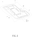
- FIG. 2 is a schematic diagram of a partial structure of an electronic device according to an embodiment of the present invention.
- an electronic device 1 includes a mainboard 2, a connector 4, an electronic module 5, a shielding device 6, and a housing baseboard 3.
- the connector 4 is arranged on the mainboard 2.
- the electronic module 5 is arranged on the mainboard 2 and electrically connected to the connector 4.
- the shielding device 6 includes a fixing frame 10 and a shielding cover 20.
- the fixing frame 10 is fixedly arranged on the mainboard 2 and is provided in a framing manner with an accommodating space S (marked in subsequent FIG. 3 ).
- the accommodating space S is suitable for accommodating the connector 4 and the electronic module 5.
- the fixing frame 10 includes a press plate 16, and the connector 4 is covered by the press plate 16.
- the shielding cover 20 is pivotally connected to one side, away from the press plate 16, of the fixing frame 10 and is suitable to be opened or closed relative to the fixing frame 10.
- the housing baseboard 3 covers part of the mainboard 2 and part of the press plate 16, and the housing baseboard 3 has an open groove 30 through which the shielding cover 20 is exposed.
- FIG. 3 is a schematic exploded view of a shielding device according to an embodiment of the present invention.
- the fixing frame 10 of the shielding device 6 includes two first side walls 12 and 12' opposite to each other, two second side walls 14 opposite to each other, and the press plate 16.
- the fixing frame 10 is provided in a framing manner with the accommodating space S, and the press plate 16 is connected to the first side wall 12'.
- the shielding cover 20 of the shielding device 6 is pivotally connected to one side, away from the press plate 16, of the fixing frame 10 and is suitable to be opened or closed relative to the fixing frame 10.
- the fixing frame 10 further includes a stepped structure 28 connecting the press plate 16 to the first side wall 12', and the stepped structure 28 is not connected to the second side walls 14.
- FIG. 4 is a schematic diagram of a shielding device in a cover closing state according to an embodiment of the present invention.
- the first side wall 12 of the fixing frame 10 that is not connected to the press plate 16 has a first surface 121
- each of the two second side walls 14 of the fixing frame 10 has a second surface 141
- a guide groove 26 is formed in one end, away from the press plate 16, of each of the two second side walls 14.
- the shielding cover 20 has a front edge 201, a back edge 202 opposite to each other, and two side edges 203 opposite to each other.
- the shielding cover 20 is provided in an extension manner with first bent portions 22 respectively located on the two side edges 203 and adjacent to the back edge 202.
- each of opposite inner sides of the two first bent portions 22 is provided with a guide rod 27.
- the guide rod 27 may be arranged in the guide groove 26 in a penetration manner and is suitable to slide and rotate in the guide groove 26 so as to drive the shielding cover 20 to be opened or closed relative to the fixing frame 10.
- the shielding cover 20 further has two second bent portions 24 respectively formed on the two side edges 203 and adjacent to the front edge 201. As shown in FIG. 4 , when closed relative to the fixing frame 10, the shielding cover 20 covers the first surface 121 (marked in FIG. 3 ) and the second surface 141, the front edge 201 of the shielding cover 20 is located on the press plate 16, the side edges 203 are parallel to the second side walls 14, and the second bent portions 24 are attached to the second side walls 14.
- each of the second bent portions 24 is provided with a clamping hole 19, and one end, adjacent to the press plate 16, of each of the second side walls 14 is provided with a bump 18.
- the bump 18 is suitable to be clamped with the clamping hole 19.
- the bump 18 and the clamping hole 19 may be arranged oppositely.
- each of opposite inner sides of the two second bent portions 24 is provided with a bump 18, and one end, adjacent to the press plate 16, of each of the second side walls 14 is provided with a clamping hole 19.
- the bump 18 is suitable to be clamped with the clamping hole 19.
- FIG. 5, FIG. 6 , and FIG. 7 are schematic sectional views of a shielding device according to an embodiment of the present invention during cover opening.
- the guide groove 26 is, for example, L-shaped.
- the guide rod 27 is located at one end, adjacent to the press plate 16, of the guide groove 26, and the shielding cover 20 will cover part of the press plate 16.
- the shielding cover 20 is about to be opened, as shown in FIG. 6 , the shielding cover 20 is first moved away from the press plate 16, and the guide rod 27 is driven to move away from the press plate 16 to a turning point of the guide groove 26, thus making the shielding cover 20 keep away from the press plate 16.
- the first surface 121 of the first side wall 12 may be slightly lower than a height of the second surface 141 (marked in FIG. 3 and FIG. 4 ), such that during the process of moving the shielding cover 20 away from the press plate 16, the shielding cover 20 will not rub against the first surface 121, thereby avoiding the shielding effect of the shielding device 6 being reduced due to wear of the first surface 121.
- the guide rod 27 rotates in the guide groove 26 and moves towards the second surface 141 in accordance with a shape of the guide groove 26, making the shielding cover 20 smoothly expose the accommodating space S.
- the electronic device 1 is, for example, a laptop, a tablet, or a display
- the mainboard 2 is, for example, a motherboard or a circuit board of the electronic device 1
- the electronic module 5 is, for example, a double data rate synchronous dynamic random access memory.
- the present invention is not limited thereto.
- the shielding device 6 provided by an embodiment of the present invention includes the shielding cover 20 and the fixing frame 10 designed in a two-piece manner.
- the fixing frame 10 is fixedly arranged on the mainboard 2 of the electronic device 1 and partially covered by the housing baseboard 3.
- the shielding cover 20 is pivotally connected to one side of the fixing frame 10 and may be opened or closed relative to the fixing frame 10 to expose or shield the electronic module 5 framed by the fixing frame 10.
- the shielding cover 20 when the user opens the shielding cover 20, the shielding cover 20 is easier to open by the user with a slidable and rotatable pivot structure formed by the guide rods 27 of the shielding cover 20 and the guide grooves 26 of the fixing frame 10.
- the shielding cover 20 may be really clamped and not prone to sliding with the mutually corresponding bumps 18 and clamping holes 19 arranged on the shielding cover 20 and the fixing frame 10.
- the shielding cover 20 and the fixing frame 10 are pivotally connected to each other, which may better avoid that the user forgetting to close the shielding cover 20 after replacing the electronic module 5 by himself and affecting the shielding effect.
Landscapes
- Engineering & Computer Science (AREA)
- Computer Hardware Design (AREA)
- Theoretical Computer Science (AREA)
- General Engineering & Computer Science (AREA)
- Physics & Mathematics (AREA)
- Human Computer Interaction (AREA)
- General Physics & Mathematics (AREA)
- Microelectronics & Electronic Packaging (AREA)
- Electromagnetism (AREA)
- Power Engineering (AREA)
- Casings For Electric Apparatus (AREA)
- Shielding Devices Or Components To Electric Or Magnetic Fields (AREA)
Abstract
A shielding device is suitable for applying in an electronic module arranged on a mainboard of an electronic device having a housing baseboard. The mainboard is provided with a connector. The shielding device includes a fixing frame and a shielding cover. The fixing frame is provided with an accommodating space suitable for accommodating the connector and the electronic module. The fixing frame includes two first side walls, two second side walls, and a press plate connecting to one of the two first side walls and covering the connector. A part of the press plate is covered by the housing baseboard. The shielding cover is pivotally connected to one side, away from the press plate, of the fixing frame and may be opened or closed relative to the fixing frame. The electronic module is exposed through opening of the shielding cover and is shielded through closing of the shielding cover.
Description
- The present invention relates to a shielding device, and more particularly to a shielding device convenient for disassembling an electronic module, and an electronic device.
- The double date rate synchronous dynamic random access memory (DDR-SDRAM) is a next-generation product following the single date rate synchronous dynamic random access memory (SDR-SDRAM). With the increasing usage requirements of people and technological innovation, the fifth-generation DDR-SDRAM (DDR5) may bring about higher channel efficiency, improved power consumption management, and optimized performance to cope with more efficient computing systems. However, because DDR5 itself generates more noisy signals, a shielding cover needs to be arranged to cover the DDR5, to prevent the noisy signals generated by the DDR5 during operation from interfering with signal transmission of other electronic components.
- The present invention provides a shielding device. A user may replace an electronic module only by opening a shielding cover without dismantling a housing baseboard of an electronic device; and the user forgetting to close the shielding cover after replacing the electronic module by himself and affecting the shielding effect may be better avoided.
- The shielding device provided by the present invention is suitable for applying in an electronic module arranged on a mainboard of an electronic device having a housing baseboard. The mainboard is provided with a connector suitable to be electrically connected to the electronic module. The shielding device includes a fixing frame and a shielding cover. The fixing frame is fixedly arranged on the mainboard and provided in a framing manner with an accommodating space suitable for accommodating the connector and the electronic module. The fixing frame includes two first side walls opposite to each other, two second side walls opposite to each other, and a press plate. The press plate is connected to one of the two first side walls and covers the connector. A part of the press plate is covered by the housing baseboard of the electronic device. The shielding cover is pivotally connected to one side, away from the press plate, of the fixing frame and is suitable to be opened or closed relative to the fixing frame, where opening of the shielding cover is suitable to expose the electronic module, and closing of the shielding cover is suitable to shield the electronic module.
- In an embodiment of the present invention, a second one of the two first side walls not connected to the press plate has a first surface, each of the two second side walls has a second surface, and when the shielding cover is closed relative to the fixing frame, the first surface and the second surface are covered by the shielding cover.
- In an embodiment of the present invention, the shielding cover has a front edge and a back edge opposite to each other, and two side edges opposite to each other, and when the shielding cover is closed relative to the fixing frame, the front edge is located on the press plate, and the two side edges are parallel to the two second side walls.
- In an embodiment of the present invention, one end, away from the press plate, of each of the two second side walls is provided with a guide groove, the shielding cover further has first bent portions formed on the side edges and adjacent to the back edge, each of the first bent portions is provided with a guide rod, and the guide rod is arranged in the guide groove in a penetration manner and is suitable to slide and rotate in the guide groove, such that the shielding cover is suitable to be opened or closed relative to the fixing frame.
- In an embodiment of the present invention, the shielding cover further has second bent portions formed on the side edges and adjacent to the front edge, and when the shielding cover is closed relative to the fixing frame, the second bent portions are attached to the second side walls.
- In an embodiment of the present invention, the shielding cover further has second bent portions formed on the side edges and adjacent to the front edge, each of the second bent portions is provided with a clamping hole, each of the two second side walls is provided with a bump adjacent to the press plate, and when the shielding cover is closed relative to the fixing frame, the bump is suitable to be clamped with the clamping hole.
- In an embodiment of the present invention, the shielding cover further has second bent portions formed on the side edges and adjacent to the front edge, an inner side of each of the second bent portions is provided with a bump, each of the second side walls is provided with a clamping hole adjacent to the press plate, and when the shielding cover is closed relative to the fixing frame, the bump is suitable to be clamped with the clamping hole.
- In an embodiment of the present invention, the fixing frame further includes a stepped structure connecting the press plate to the one of the first side walls or a second one of the two first side walls, and the stepped structure is not connected to the second side walls.
- In an embodiment of the present invention, the fixing frame is integrally formed.
- The electronic device provided by the present invention includes a mainboard, a shielding device, a connector, an electronic module, and a housing baseboard. The shielding device includes a fixing frame and a shielding cover. The fixing frame is fixedly arranged on the mainboard and provided in a framing manner with an accommodating space. The fixing frame includes two first side walls opposite to each other, two second side walls opposite to each other, and a press plate. The press plate is connected to one of the two first side walls. The shielding cover is pivotally connected to one side, away from the press plate, of the fixing frame and is suitable to be opened or closed relative to the fixing frame. The connector is arranged on the mainboard and located in the accommodating space. The electronic module is arranged in the accommodating space and is suitable to be electrically connected to the connector. Opening of the shielding cover is suitable to expose the electronic module, and closing of the shielding cover is suitable to shield the electronic module. The housing baseboard covers part of the mainboard and part of the press plate, and has an open groove through which at least the shielding cover is exposed.
- In an embodiment of the present invention, the connector is covered by the press plate.
- In an embodiment of the present invention, the electronic module is a double data rate synchronous dynamic random access memory.
- The shielding device according to the present invention includes the shielding cover and the fixing frame designed in a two-piece manner. The fixing frame is fixedly arranged on the mainboard of the electronic device and partially covered by the housing baseboard. The shielding cover is pivotally connected to one side of the fixing frame and may be opened or closed relative to the fixing frame to expose or shield the electronic module framed by the fixing frame. Because the shielding cover may be freely opened or closed relative to the fixing frame, it is convenient for a user to disassemble the electronic module.
- The present invention will become more readily apparent to those ordinarily skilled in the art after reviewing the following detailed description and accompanying drawings, in which:
-
FIG. 1 is a schematic partial exploded view of an electronic device according to an embodiment of the present invention; -
FIG. 2 is a schematic diagram of a partial structure of an electronic device according to an embodiment of the present invention; -
FIG. 3 is a schematic exploded view of a shielding device according to an embodiment of the present invention; -
FIG. 4 is a schematic diagram of a shielding device in a cover closing state according to an embodiment of the present invention; and -
FIG. 5, FIG. 6 , andFIG. 7 are schematic sectional views of a shielding device in a cover opening process according to an embodiment of the present invention. - The present invention will now be described more specifically with reference to the following embodiments. It is to be noted that the following descriptions of preferred embodiments of this invention are presented herein for purpose of illustration and description only. It is not intended to be exhaustive or to be limited to the precise form disclosed.
-
FIG. 1 is a schematic partial exploded view of an electronic device according to an embodiment of the present invention.FIG. 2 is a schematic diagram of a partial structure of an electronic device according to an embodiment of the present invention. As shown inFIG. 1 andFIG. 2 , anelectronic device 1 includes amainboard 2, a connector 4, anelectronic module 5, ashielding device 6, and ahousing baseboard 3. The connector 4 is arranged on themainboard 2. Theelectronic module 5 is arranged on themainboard 2 and electrically connected to the connector 4. Theshielding device 6 includes afixing frame 10 and ashielding cover 20. Thefixing frame 10 is fixedly arranged on themainboard 2 and is provided in a framing manner with an accommodating space S (marked in subsequentFIG. 3 ). The accommodating space S is suitable for accommodating the connector 4 and theelectronic module 5. In an embodiment, thefixing frame 10 includes apress plate 16, and the connector 4 is covered by thepress plate 16. Theshielding cover 20 is pivotally connected to one side, away from thepress plate 16, of thefixing frame 10 and is suitable to be opened or closed relative to thefixing frame 10. Thehousing baseboard 3 covers part of themainboard 2 and part of thepress plate 16, and thehousing baseboard 3 has anopen groove 30 through which theshielding cover 20 is exposed. - Continuing with the above description,
FIG. 3 is a schematic exploded view of a shielding device according to an embodiment of the present invention. As shown inFIG. 3 , thefixing frame 10 of theshielding device 6 includes twofirst side walls 12 and 12' opposite to each other, twosecond side walls 14 opposite to each other, and thepress plate 16. The fixingframe 10 is provided in a framing manner with the accommodating space S, and thepress plate 16 is connected to the first side wall 12'. The shieldingcover 20 of theshielding device 6 is pivotally connected to one side, away from thepress plate 16, of the fixingframe 10 and is suitable to be opened or closed relative to the fixingframe 10. In an embodiment, the fixingframe 10 further includes a steppedstructure 28 connecting thepress plate 16 to the first side wall 12', and the steppedstructure 28 is not connected to thesecond side walls 14. -
FIG. 4 is a schematic diagram of a shielding device in a cover closing state according to an embodiment of the present invention. Specifically, as shown inFIG. 3 and FIG. 4 , in an embodiment, thefirst side wall 12 of the fixingframe 10 that is not connected to thepress plate 16 has afirst surface 121, each of the twosecond side walls 14 of the fixingframe 10 has asecond surface 141, and aguide groove 26 is formed in one end, away from thepress plate 16, of each of the twosecond side walls 14. The shieldingcover 20 has afront edge 201, aback edge 202 opposite to each other, and twoside edges 203 opposite to each other. The shieldingcover 20 is provided in an extension manner with firstbent portions 22 respectively located on the twoside edges 203 and adjacent to theback edge 202. Each of opposite inner sides of the two firstbent portions 22 is provided with aguide rod 27. Theguide rod 27 may be arranged in theguide groove 26 in a penetration manner and is suitable to slide and rotate in theguide groove 26 so as to drive the shieldingcover 20 to be opened or closed relative to the fixingframe 10. In an embodiment, the shieldingcover 20 further has two secondbent portions 24 respectively formed on the twoside edges 203 and adjacent to thefront edge 201. As shown inFIG. 4 , when closed relative to the fixingframe 10, the shieldingcover 20 covers the first surface 121 (marked inFIG. 3 ) and thesecond surface 141, thefront edge 201 of the shieldingcover 20 is located on thepress plate 16, the side edges 203 are parallel to thesecond side walls 14, and the secondbent portions 24 are attached to thesecond side walls 14. - In an embodiment, each of the second
bent portions 24 is provided with a clampinghole 19, and one end, adjacent to thepress plate 16, of each of thesecond side walls 14 is provided with abump 18. When the shieldingcover 20 is closed relative to the fixingframe 10, thebump 18 is suitable to be clamped with the clampinghole 19. Thebump 18 and the clampinghole 19 may be arranged oppositely. In an embodiment not shown, each of opposite inner sides of the two secondbent portions 24 is provided with abump 18, and one end, adjacent to thepress plate 16, of each of thesecond side walls 14 is provided with a clampinghole 19. When the shieldingcover 20 is closed relative to the fixingframe 10, thebump 18 is suitable to be clamped with the clampinghole 19. -
FIG. 5, FIG. 6 , andFIG. 7 are schematic sectional views of a shielding device according to an embodiment of the present invention during cover opening. As shown inFIG. 5 , theguide groove 26 is, for example, L-shaped. When the shieldingcover 20 covers the fixingframe 10, theguide rod 27 is located at one end, adjacent to thepress plate 16, of theguide groove 26, and the shieldingcover 20 will cover part of thepress plate 16. When the shieldingcover 20 is about to be opened, as shown inFIG. 6 , the shieldingcover 20 is first moved away from thepress plate 16, and theguide rod 27 is driven to move away from thepress plate 16 to a turning point of theguide groove 26, thus making the shieldingcover 20 keep away from thepress plate 16. In this case, there is a gap between thefront edge 201 of the shieldingcover 20 and thepress plate 16 to facilitate opening the shieldingcover 20. In an embodiment, thefirst surface 121 of thefirst side wall 12 may be slightly lower than a height of the second surface 141 (marked inFIG. 3 and FIG. 4 ), such that during the process of moving the shieldingcover 20 away from thepress plate 16, the shieldingcover 20 will not rub against thefirst surface 121, thereby avoiding the shielding effect of theshielding device 6 being reduced due to wear of thefirst surface 121. As shown inFIG. 7 , when the shieldingcover 20 is opened relative to the fixingframe 10, theguide rod 27 rotates in theguide groove 26 and moves towards thesecond surface 141 in accordance with a shape of theguide groove 26, making the shieldingcover 20 smoothly expose the accommodating space S. - In an embodiment, the shielding
cover 20 further has a thirdbent portion 25 arranged on theback edge 202 of the shieldingcover 20. As shown inFIG. 6 , when the shieldingcover 20 moves away from thepress plate 16, the thirdbent portion 25 is located in a spaced manner on an outer side of thefirst side wall 12. As shown inFIG. 7 , when the shieldingcover 20 is opened relative to the fixingframe 10, the thirdbent portion 25 may abut against the outer side of thefirst side wall 12. In an embodiment, the fixingframe 10 is integrally formed. - In an embodiment, the
electronic device 1 is, for example, a laptop, a tablet, or a display, themainboard 2 is, for example, a motherboard or a circuit board of theelectronic device 1, and theelectronic module 5 is, for example, a double data rate synchronous dynamic random access memory. However, the present invention is not limited thereto. - According to the above, the
shielding device 6 provided by an embodiment of the present invention includes the shieldingcover 20 and the fixingframe 10 designed in a two-piece manner. The fixingframe 10 is fixedly arranged on themainboard 2 of theelectronic device 1 and partially covered by thehousing baseboard 3. The shieldingcover 20 is pivotally connected to one side of the fixingframe 10 and may be opened or closed relative to the fixingframe 10 to expose or shield theelectronic module 5 framed by the fixingframe 10. Due to a two-piece structure of the shieldingcover 20 and the fixingframe 10, when theshielding device 6 is covered by thehousing baseboard 3, only part of the fixingframe 10 is covered/pressed, and the opening and closing of the shieldingcover 20 are not limited by thehousing baseboard 3, such that the shieldingcover 20 may be freely opened or closed relative to the fixingframe 10, thereby facilitating a user disassembling theelectronic module 5. This solves the problem of inconvenience caused by the shieldingcover 20 currently used on the market being covered by thehousing baseboard 3 of theelectronic device 1 due to spatial limitations of a machine type after covering theelectronic module 5, such that when the user needs to replace theelectronic module 5, thehousing baseboard 3 and the shieldingcover 20 must be removed before theelectronic module 5 is disassembled. - Further, when the user opens the shielding
cover 20, the shieldingcover 20 is easier to open by the user with a slidable and rotatable pivot structure formed by theguide rods 27 of the shieldingcover 20 and theguide grooves 26 of the fixingframe 10. When the user closes the shieldingcover 20, the shieldingcover 20 may be really clamped and not prone to sliding with the mutually correspondingbumps 18 and clampingholes 19 arranged on the shieldingcover 20 and the fixingframe 10. Furthermore, the shieldingcover 20 and the fixingframe 10 are pivotally connected to each other, which may better avoid that the user forgetting to close the shieldingcover 20 after replacing theelectronic module 5 by himself and affecting the shielding effect. - While the invention has been described in terms of what is presently considered to be the most practical and preferred embodiments, it is to be understood that the invention needs not be limited to the disclosed embodiment. On the contrary, it is intended to cover various modifications and similar arrangements included within the spirit and scope of the appended claims which are to be accorded with the broadest interpretation so as to encompass all such modifications and similar structures.
Claims (12)
- A shielding device (6) configured for applying in an electronic module (5) arranged on a mainboard (2) of an electronic device (1) having a housing baseboard (3), the mainboard (2) being provided with a connector (4) configured to be electrically connected to the electronic module (5), the shielding device (6) comprising:a fixing frame (10) fixedly arranged on the mainboard (2) and provided in a framing manner with an accommodating space (S) configured for accommodating the connector (4) and the electronic module (5), wherein the fixing frame (10) comprises two first side walls (12, 12') opposite to each other, two second side walls (14) opposite to each other, and a press plate (16), the press plate (16) is connected to one of the two first side walls (12, 12') and covers the connector (4), and a part of the press plate (16) is covered by the housing baseboard (3); anda shielding cover (20) pivotally connected to one side, away from the press plate (16), of the fixing frame (10) and configured to be opened or closed relative to the fixing frame (10), wherein opening of the shielding cover (20) is configured to expose the electronic module (5), and closing of the shielding cover (20) is configured to shield the electronic module (5).
- The shielding device (6) according to claim 1, wherein a second one of the two first side walls (12, 12') not connected to the press plate (16) has a first surface (121), each of the two second side walls (14) has a second surface (141), and when the shielding cover (20) is closed relative to the fixing frame (10), the first surface (121) and the second surface (141) are covered by the shielding cover (20).
- The shielding device (6) according to claim 1 or 2, wherein the shielding cover (20) has a front edge (201) and a back edge (202) opposite to each other, and two side edges (203) opposite to each other, and when the shielding cover (20) is closed relative to the fixing frame (10), the front edge (201) is located on the press plate (16), and the two side edges (203) are parallel to the two second side walls (14).
- The shielding device (6) according to claim 3, wherein one end, away from the press plate (16), of each of the two second side walls (14) is provided with a guide groove (26), the shielding cover (20) further has two first bent portions (22) respectively formed on the two side edges (203) and adjacent to the back edge (202), each of the two first bent portions (22) is provided with a guide rod (27), and the guide rod (27) is arranged in the guide groove (26) in a penetration manner and is configured to slide and rotate in the guide groove (26), such that the shielding cover (20) is configured to be opened or closed relative to the fixing frame (10).
- The shielding device (6) according to claim 2, 3 or 4, wherein the shielding cover (20) further has two second bent portions (24) respectively formed on the two side edges (203) and adjacent to the front edge (201), and when the shielding cover (20) is closed relative to the fixing frame (10), the two second bent portions (24) are attached to the two second side walls (14), respectively.
- The shielding device (6) according to any of claims 3 to 5, wherein the shielding cover (20) further has two second bent portions (24) respectively formed on the two side edges (203) and adjacent to the front edge (201), each of the two second bent portions (24) is provided with a clamping hole (19), each of the two second side walls (14) is provided with a bump (18) adjacent to the press plate (16), and when the shielding cover (20) is closed relative to the fixing frame (10), the bump (18) is configured to be clamped with the clamping hole (19).
- The shielding device (6) according to any of claims 3 to 5, wherein the shielding cover (20) further has two second bent portions (24) respectively formed on the two side edges (203) and adjacent to the front edge (201), an inner side of each of the two second bent portions (24) is provided with a bump (18), each of the two second side walls (14) is provided with a clamping hole (19) adjacent to the press plate (16), and when the shielding cover (20) is closed relative to the fixing frame (10), the bump (18) is configured to be clamped with the clamping hole (19).
- The shielding device (6) according to any of the preceding claims, wherein the fixing frame (10) further comprises a stepped structure (28) connecting the press plate (16) to the one of the two first side walls (12, 12') or a second one of the two first side walls (12, 12'), and the stepped structure (28) is not connected to the two second side walls (14).
- The shielding device (6) according to any of the preceding claims, wherein the fixing frame (10) is integrally formed.
- An electronic device (1), comprising:a mainboard (2);a shielding device (6) comprising:a fixing frame (10) fixedly arranged on the mainboard (2) and provided in a framing manner with an accommodating space (S), wherein the fixing frame (10) comprises two first side walls (12, 12') opposite to each other, two second side walls (14) opposite to each other, and a press plate (16), and the press plate (16) is connected to one of the two first side walls (12, 12'); anda shielding cover (20) pivotally connected to one side, away from the press plate (16), of the fixing frame (10) and configured to be opened or closed relative to the fixing frame (10);a connector (4) arranged on the mainboard (2) and located in the accommodating space (S);an electronic module (5) arranged in the accommodating space (S) and configured to be electrically connected to the connector (4), wherein opening of the shielding cover (20) is configured to expose the electronic module (5), and closing of the shielding cover (20) is configured to shield the electronic module (5); anda housing baseboard (3) covering part of the mainboard (2) and part of the press plate (16), wherein the housing baseboard (3) has an open groove (30) through which at least the shielding cover (20) is exposed.
- The electronic device (1) according to claim 10, wherein the connector (4) is covered by the press plate (16).
- The electronic device (1) according to claim 10 or 11, wherein the electronic module (5) is a double data rate synchronous dynamic random access memory.
Applications Claiming Priority (1)
| Application Number | Priority Date | Filing Date | Title |
|---|---|---|---|
| CN202311469803.7A CN119967793A (en) | 2023-11-07 | 2023-11-07 | Shielding device and electronic device |
Publications (1)
| Publication Number | Publication Date |
|---|---|
| EP4553612A1 true EP4553612A1 (en) | 2025-05-14 |
Family
ID=92503730
Family Applications (1)
| Application Number | Title | Priority Date | Filing Date |
|---|---|---|---|
| EP24195584.8A Pending EP4553612A1 (en) | 2023-11-07 | 2024-08-21 | Shielding device and electronic device |
Country Status (3)
| Country | Link |
|---|---|
| US (1) | US20250149833A1 (en) |
| EP (1) | EP4553612A1 (en) |
| CN (1) | CN119967793A (en) |
Cited By (1)
| Publication number | Priority date | Publication date | Assignee | Title |
|---|---|---|---|---|
| EP4625105A1 (en) * | 2024-03-29 | 2025-10-01 | INTEL Corporation | Electromagnetic interference shield extending underneath memory modules |
Citations (3)
| Publication number | Priority date | Publication date | Assignee | Title |
|---|---|---|---|---|
| EP0726700B1 (en) * | 1995-02-07 | 1999-03-17 | Nokia Mobile Phones Ltd. | A shielding device |
| US7208675B2 (en) * | 2005-06-24 | 2007-04-24 | Chin-Hsing Horng | Shielding cover |
| US20180310441A1 (en) * | 2017-04-20 | 2018-10-25 | Compal Electronics, Inc. | Electronic assembly with rfi shielding |
-
2023
- 2023-11-07 CN CN202311469803.7A patent/CN119967793A/en active Pending
-
2024
- 2024-07-17 US US18/775,183 patent/US20250149833A1/en active Pending
- 2024-08-21 EP EP24195584.8A patent/EP4553612A1/en active Pending
Patent Citations (3)
| Publication number | Priority date | Publication date | Assignee | Title |
|---|---|---|---|---|
| EP0726700B1 (en) * | 1995-02-07 | 1999-03-17 | Nokia Mobile Phones Ltd. | A shielding device |
| US7208675B2 (en) * | 2005-06-24 | 2007-04-24 | Chin-Hsing Horng | Shielding cover |
| US20180310441A1 (en) * | 2017-04-20 | 2018-10-25 | Compal Electronics, Inc. | Electronic assembly with rfi shielding |
Cited By (2)
| Publication number | Priority date | Publication date | Assignee | Title |
|---|---|---|---|---|
| EP4625105A1 (en) * | 2024-03-29 | 2025-10-01 | INTEL Corporation | Electromagnetic interference shield extending underneath memory modules |
| US12621970B2 (en) | 2024-03-29 | 2026-05-05 | Intel Corporation | Electromagnetic interference shield extending underneath memory modules |
Also Published As
| Publication number | Publication date |
|---|---|
| US20250149833A1 (en) | 2025-05-08 |
| CN119967793A (en) | 2025-05-09 |
Similar Documents
| Publication | Publication Date | Title |
|---|---|---|
| TWI681284B (en) | Pivot mechanism and flexible electronic device | |
| US5559672A (en) | Door apparatus for a portable computer | |
| US5557288A (en) | Antenna housing with extendable drawer for a portable computer | |
| US9196994B2 (en) | Connector mechanism and related electronic device | |
| US20250149833A1 (en) | Shielding device and electronic device | |
| US8576558B2 (en) | Mounting apparatus with rotating member for retaining and buffering data storage device | |
| US8045088B2 (en) | Liquid crystal display device having metal shield with fixing unit and shielding unit | |
| JP2001036265A (en) | Electronic system with printed circuit board mounting equipment | |
| CN203085824U (en) | Connector mechanism and electronic device | |
| US11962878B2 (en) | Electronic device | |
| US8840416B2 (en) | Portable electronic device | |
| US20060290246A1 (en) | Rotating machanism of drive bracket | |
| US7448898B2 (en) | Information processing apparatus having a mounting slot and mounting slot door thereof | |
| CN203025621U (en) | Tool-less swivel computer peripheral assembly labor saver | |
| CN108282175B (en) | A kind of card tray structure and mobile terminal | |
| TWI897088B (en) | Shielding device and electronic device | |
| CN109992048B (en) | an electronic device | |
| CN209164356U (en) | A kind of hinge arrangement and laptop | |
| TW201724948A (en) | Portable electronic device | |
| US11822378B1 (en) | Control panel assemblies having rotatable input devices | |
| TWI678956B (en) | Opening and closing structure and electronic device with same | |
| CN203930626U (en) | Network storage devices and enclosures | |
| CN111399589B (en) | Pivot mechanism and flexible electronic device | |
| JP2001250631A (en) | Connector for ic card | |
| CN106351941B (en) | Rotating shaft assembly and electronic equipment |
Legal Events
| Date | Code | Title | Description |
|---|---|---|---|
| PUAI | Public reference made under article 153(3) epc to a published international application that has entered the european phase |
Free format text: ORIGINAL CODE: 0009012 |
|
| STAA | Information on the status of an ep patent application or granted ep patent |
Free format text: STATUS: THE APPLICATION HAS BEEN PUBLISHED |
|
| AK | Designated contracting states |
Kind code of ref document: A1 Designated state(s): AL AT BE BG CH CY CZ DE DK EE ES FI FR GB GR HR HU IE IS IT LI LT LU LV MC ME MK MT NL NO PL PT RO RS SE SI SK SM TR |
|
| STAA | Information on the status of an ep patent application or granted ep patent |
Free format text: STATUS: REQUEST FOR EXAMINATION WAS MADE |
|
| 17P | Request for examination filed |
Effective date: 20250818 |