EP4550978A1 - Power semiconductor device and associated methods - Google Patents
Power semiconductor device and associated methods Download PDFInfo
- Publication number
- EP4550978A1 EP4550978A1 EP24209922.4A EP24209922A EP4550978A1 EP 4550978 A1 EP4550978 A1 EP 4550978A1 EP 24209922 A EP24209922 A EP 24209922A EP 4550978 A1 EP4550978 A1 EP 4550978A1
- Authority
- EP
- European Patent Office
- Prior art keywords
- region
- pillar
- doping concentration
- type dopant
- conductivity type
- Prior art date
- Legal status (The legal status is an assumption and is not a legal conclusion. Google has not performed a legal analysis and makes no representation as to the accuracy of the status listed.)
- Pending
Links
Images







Classifications
-
- H—ELECTRICITY
- H10—SEMICONDUCTOR DEVICES; ELECTRIC SOLID-STATE DEVICES NOT OTHERWISE PROVIDED FOR
- H10D—INORGANIC ELECTRIC SEMICONDUCTOR DEVICES
- H10D62/00—Semiconductor bodies, or regions thereof, of devices having potential barriers
- H10D62/01—Manufacture or treatment
- H10D62/051—Forming charge compensation regions, e.g. superjunctions
- H10D62/058—Forming charge compensation regions, e.g. superjunctions by using trenches, e.g. implanting into sidewalls of trenches or refilling trenches
-
- H—ELECTRICITY
- H10—SEMICONDUCTOR DEVICES; ELECTRIC SOLID-STATE DEVICES NOT OTHERWISE PROVIDED FOR
- H10D—INORGANIC ELECTRIC SEMICONDUCTOR DEVICES
- H10D12/00—Bipolar devices controlled by the field effect, e.g. insulated-gate bipolar transistors [IGBT]
- H10D12/411—Insulated-gate bipolar transistors [IGBT]
- H10D12/441—Vertical IGBTs
-
- H—ELECTRICITY
- H10—SEMICONDUCTOR DEVICES; ELECTRIC SOLID-STATE DEVICES NOT OTHERWISE PROVIDED FOR
- H10D—INORGANIC ELECTRIC SEMICONDUCTOR DEVICES
- H10D30/00—Field-effect transistors [FET]
- H10D30/01—Manufacture or treatment
- H10D30/021—Manufacture or treatment of FETs having insulated gates [IGFET]
- H10D30/028—Manufacture or treatment of FETs having insulated gates [IGFET] of double-diffused metal oxide semiconductor [DMOS] FETs
- H10D30/0291—Manufacture or treatment of FETs having insulated gates [IGFET] of double-diffused metal oxide semiconductor [DMOS] FETs of vertical DMOS [VDMOS] FETs
-
- H—ELECTRICITY
- H10—SEMICONDUCTOR DEVICES; ELECTRIC SOLID-STATE DEVICES NOT OTHERWISE PROVIDED FOR
- H10D—INORGANIC ELECTRIC SEMICONDUCTOR DEVICES
- H10D30/00—Field-effect transistors [FET]
- H10D30/60—Insulated-gate field-effect transistors [IGFET]
- H10D30/64—Double-diffused metal-oxide semiconductor [DMOS] FETs
- H10D30/66—Vertical DMOS [VDMOS] FETs
-
- H—ELECTRICITY
- H10—SEMICONDUCTOR DEVICES; ELECTRIC SOLID-STATE DEVICES NOT OTHERWISE PROVIDED FOR
- H10D—INORGANIC ELECTRIC SEMICONDUCTOR DEVICES
- H10D62/00—Semiconductor bodies, or regions thereof, of devices having potential barriers
- H10D62/01—Manufacture or treatment
- H10D62/051—Forming charge compensation regions, e.g. superjunctions
- H10D62/052—Forming charge compensation regions, e.g. superjunctions by forming stacked epitaxial layers
-
- H—ELECTRICITY
- H10—SEMICONDUCTOR DEVICES; ELECTRIC SOLID-STATE DEVICES NOT OTHERWISE PROVIDED FOR
- H10D—INORGANIC ELECTRIC SEMICONDUCTOR DEVICES
- H10D62/00—Semiconductor bodies, or regions thereof, of devices having potential barriers
- H10D62/10—Shapes, relative sizes or dispositions of the regions of the semiconductor bodies; Shapes of the semiconductor bodies
- H10D62/102—Constructional design considerations for preventing surface leakage or controlling electric field concentration
- H10D62/103—Constructional design considerations for preventing surface leakage or controlling electric field concentration for increasing or controlling the breakdown voltage of reverse-biased devices
- H10D62/105—Constructional design considerations for preventing surface leakage or controlling electric field concentration for increasing or controlling the breakdown voltage of reverse-biased devices by having particular doping profiles, shapes or arrangements of PN junctions; by having supplementary regions, e.g. junction termination extension [JTE]
- H10D62/109—Reduced surface field [RESURF] PN junction structures
- H10D62/111—Multiple RESURF structures, e.g. double RESURF or 3D-RESURF structures
-
- H—ELECTRICITY
- H10—SEMICONDUCTOR DEVICES; ELECTRIC SOLID-STATE DEVICES NOT OTHERWISE PROVIDED FOR
- H10D—INORGANIC ELECTRIC SEMICONDUCTOR DEVICES
- H10D62/00—Semiconductor bodies, or regions thereof, of devices having potential barriers
- H10D62/10—Shapes, relative sizes or dispositions of the regions of the semiconductor bodies; Shapes of the semiconductor bodies
- H10D62/13—Semiconductor regions connected to electrodes carrying current to be rectified, amplified or switched, e.g. source or drain regions
- H10D62/149—Source or drain regions of field-effect devices
- H10D62/151—Source or drain regions of field-effect devices of IGFETs
- H10D62/156—Drain regions of DMOS transistors
- H10D62/159—Shapes
-
- H—ELECTRICITY
- H10—SEMICONDUCTOR DEVICES; ELECTRIC SOLID-STATE DEVICES NOT OTHERWISE PROVIDED FOR
- H10P—GENERIC PROCESSES OR APPARATUS FOR THE MANUFACTURE OR TREATMENT OF DEVICES COVERED BY CLASS H10
- H10P30/00—Ion implantation into wafers, substrates or parts of devices
- H10P30/20—Ion implantation into wafers, substrates or parts of devices into semiconductor materials, e.g. for doping
- H10P30/22—Ion implantation into wafers, substrates or parts of devices into semiconductor materials, e.g. for doping using masks
Definitions
- the present disclosure relates to a power semiconductor device and a method of manufacturing a power semiconductor device. Particularly but not exclusively, the present disclosure relates to a super junction (SJ) metal-oxide semiconductor field-effect transistor (MOSFET).
- SJ super junction
- MOSFET metal-oxide semiconductor field-effect transistor
- Power semiconductor devices such as metal-oxide semiconductor field-effect transistors (MOSFETs) or insulated-gate bipolar transistors (IGBTs) require a high breakdown voltage. It is possible to achieve a high value of breakdown voltage in the active regions of super junction MOSFETS, for example by using a number of thin semiconductor layers in the super junction area to create charge balance.
- FOM Figure of Merit
- a doping concentration in the super junction region of the MOSFET may be increased to decrease the specific resistance.
- this can also lead to a decrease of the breakdown voltage, which may be due to an increased electric field at a top portion of the super junction region compared to an electric field at a bottom portion of the super junction region.
- US 9,595,596 B2 relates to a power device
- US 9,024,381 B2 relates to a semiconductor device
- US6630698B1 relates to a high-voltage semiconductor component
- US 8,283,720 B2 relates to power semiconductor device.
- a semiconductor power device comprising an active region, the active region comprising:
- a breakdown voltage of the device may be increased. This in turn may lead to an increase in a ratio of the breakdown voltage over a specific resistance of the device. This ratio may also be referred to the Figure of Merit (FOM).
- FOM Figure of Merit
- an electric field at a top or a surface of the active region may be decreased. This may lead to a more even distribution of the electric field in the active region of the device.
- the effect of decreasing of the electric field at the top or surface of the active region may also be referred to as Reduced Surface Field (RESURF).
- RESURF Reduced Surface Field
- an impact ionisation location of the device may be located at a bottom of the super junction region, e.g. proximal to the drift region. This may result in an improved non-latch-up performance of the device. The improved latch-up performance may in turn result in a more even distribution of heat generated in the device.
- the doping concentration of the portion of the second pillar may decrease linearly in the direction along the portion of the second pillar from the drift region to the body region.
- the doping concentration of the first pillar may increase linearly in the direction along the first pillar from the drift region to the body region.
- the doping concentration of the portion of the second pillar may decrease stepwise in the direction along the portion of the second pillar from the drift region to the body region.
- the doping concentration of the first pillar may increase stepwise in the direction along the first pillar from the drift region to the body region.
- the doping concentration of the portion of the second pillar may decrease in two or more steps.
- the doping concentration of the first pillar may increase in two or more steps.
- the doping concentration of the first pillar at or near the body region may be larger, smaller or the same as the doping concentration of the portion of the second pillar at or near the body region.
- the super junction region may comprises a plurality of first pillars and a plurality of second pillars.
- the plurality of first pillars and the plurality of second pillars may be alternately arranged with each other.
- the portion of the second pillar may be part of or comprised in at least one second pillar of the plurality of second pillars.
- Each of the plurality of first pillars may arranged adjacent at least one of the plurality of second pillars.
- Each of the plurality of first pillars may form a p-n-junction with the at least one of the plurality of second pillars.
- the semiconductor device may comprise a metal-oxide-semiconductor field-effect transistor (MOSFET) or an insulated-gate bipolar transistor (IGBT).
- MOSFET metal-oxide-semiconductor field-effect transistor
- IGBT insulated-gate bipolar transistor
- the first pillar or each of the plurality of first pillars may comprise or define a further drift region.
- the portion of the second pillar, the second pillar or each of the plurality of second pillars may comprise or define a partition region.
- a method of manufacturing an active region of a semiconductor power device comprising:
- Forming the super junction region may comprise: performing each of steps (i) to (v) one or more times:
- the semiconductor layer may be deposited on the drift region.
- a subsequent semiconductor layer may be deposited on a previously deposited semiconductor layer.
- a doping concentration of each first region of the first conductivity type may be the same.
- a doping concentration of a second region of the second conductivity type formed in the at least one subsequent iteration may be decreased relative to a doping concentration of a second region of the second conductivity type formed in a previous iteration.
- a doping concentration of each second region of the second conductivity type may be the same.
- a doping concentration of a first region of the first conductivity type formed in the at least one subsequent iteration may be increased relative to a doping concentration of a first region of the first conductivity type formed in a previous iteration.
- Forming the super junction region may comprise forming a trench in a semiconductor region of a first conductivity type.
- the method may comprise forming the body region prior to forming the trench.
- the trench may be formed such that the trench extends through the body region into semiconductor region.
- the trench may extend into the semiconductor region in a vertical direction.
- the trench may be formed such that the trench is in contact with the body region.
- the trench may be formed such that the trench is in contact with the drift region.
- a portion of the semiconductor region that is located adjacent to the trench may form the first pillar.
- Forming the super junction region may comprise filling the trench with a semiconductor material of a second conductivity type to form at least the portion of the second pillar.
- a method of manufacturing a semiconductor power device comprising manufacturing an active region of the semiconductor power device according to the second aspect.
- Figures 1 and 2 show schematically a cross-section of an active region 105 of a semiconductor device 100.
- the active region 105 shown in Figure 1 may be considered as a unit cell, which may be repeated thousands of times in the device 100.
- the active region 105 shown in Figure 2 may be considered as a half of the unit cell shown in Figure 1 .
- the device 100 is a silicon based super junction MOSFET.
- the device may comprise one or more alternative semiconductor materials.
- the device may alternatively be silicon carbide (SiC) or Gallium Nitride (GaN) based.
- the active region 105 comprises a substrate 110 of a first conductivity type.
- the substrate 110 may comprise an n-type doped semiconductor material, such as n + silicon.
- An n-type dopant concentration of the substrate 110 may be larger than about 5 x 10 18 cm -3 .
- the substrate 110 is conductive and acts as a drain region.
- a thickness of the substrate may be between about 40 ⁇ m and about 100 ⁇ m.
- the active region 105 comprises a drift region 115 arranged on the substrate 110.
- the drift region 115 comprises an n-type doped semiconductor material, such as n-type doped silicon.
- An n-type dopant concentration of the drift region 115 may be between about 5 x 10 14 cm -3 and 5 x 10 17 cm -3 , such as about 7 x 10 15 cm -3 .
- the drift region 115 may also be referred to as an n-drift region, n-type buffer region or n-type voltage sustaining region.
- the drift region 115 is formed on or over the semiconductor substrate 110.
- the drift region 115 comprises one or more epitaxial layers and has a thickness of about 15 ⁇ m. However, it will be appreciated that in other embodiments, the drift region may have a thickness that is more or less than 15 ⁇ m.
- a drain contact 110a may be arranged on an underside of the substrate 110, e.g. a side of the substrate 110 that is opposite to the drift region 110.
- the drain contact 110a may comprise a conductive material, such as a metal material.
- the metal material may comprise a metal alloy, such as titanium nickel silver or another metal alloy.
- the active area 105 includes a body region 120 of a second conductivity type.
- the second conductivity type is opposite to the first conductivity type.
- the body region 120 comprises a p-type semiconductor material.
- the active area 105 includes a super junction region 125.
- the super junction region 125 is arranged between the drift region 115 and the body region 120.
- the super junction region 125 comprises a plurality of first pillars 125a of the first conductivity type and a plurality of second pillars 125b of the second conductivity type.
- each first pillar 125a is an n-type pillar and each second pillar 125b is a p-type pillar.
- the first pillars 125a may define further drift regions.
- the second pillars 125b may define partition regions.
- the first and second pillars 125a, 125b are alternately arranged and in contact with each other.
- each first pillar 125a is arranged between two adjacent second pillars 125b.
- the super junction region 125 comprises a first pillar 125a and two portions of two respective second pillars 125b.
- the first pillar 125a is arranged between the two portions the second pillars 125b.
- the super junction region comprises a portion of the first pillar 125a and a portion of the second pillar 125b.
- the portions of the first and second pillars 125a, 125b are arranged adjacent to each other. This arrangement results in the formation of parallel p-n-junctions extending in a vertical direction between the drift region 115 and the body region 120.
- the super junction region 125 may also be referred to as a p-n-junction region.
- a width of each of the first and second pillars 125a, 125b may be about 3.5 ⁇ m.
- a height of each of the first and second pillars 125a, 125b may be between about 3 ⁇ m and 6 ⁇ m.
- the first and second pillars are not limited to having the exemplary height and/or width disclosed herein.
- the active region 105 comprises an n-type doped JFET region 130.
- the JFET region is arranged above the first pillar 125a.
- the JFET region 130 is arranged to extend from the first pillar to an upper surface of the body region 120.
- the body region 120 is arranged on either side of the JFET region 130.
- the active region 105 comprises a gate conductive region 135.
- the gate conductive region 135 is located above the JFET region 130 and the body region 120.
- the gate conductive region 135 is used to control a conduction channel in the active region 105.
- the active region 105 comprises a first insulation region 140a.
- the first insulation region 140a is arranged between the JFET region 130 and the gate conductive region 135.
- the first insulation region 140a may extend along the sides of the gate conductive region 135.
- the first insulation region may be referred to as a gate oxide region 140a.
- the active region 105 comprises a second insulation region 140b.
- the second insulation region 140b is arranged on or over the gate conductive region 135 and the gate oxide region 140a.
- the second insulation region may also be referred to as an interlayer dielectric layer 140b.
- the device 100 includes source contact regions, which in this example are n + source contact regions 145.
- the n + source contact regions 145 are arranged on either side of the JFET region 130 and below the gate oxide region 140a.
- a conduction channel is formed between the n + source contact regions 145 and the drift region 115 by application of a positive voltage to the gate conductive region 135.
- the body region 120 comprises a contact region, which in this example comprises p + contact regions 150.
- the p + contact regions 150 are formed on either side of the JFET region 130 and adjacent a respective n + source contact 145 region.
- the device 100 comprises a source contact 155.
- the source contact 155 may comprise a conductive material, such as a metal material.
- the metal material may comprise aluminium, tungsten, titanium or a combination thereof.
- the source contact 155 is located on an upper surface of the device.
- the source contact 155 may be arranged on or over the interlayer dielectric layer 140b.
- the source contact 155 may also be arranged to contact the n + source contact 145 regions and the p + contact regions 150.
- a lateral extension or a width of the unit cell of the device 100 is about 7 ⁇ m.
- the lateral extension or cell pitch may be more or less than 7 ⁇ m.
- the lateral extension or the width of the unit cell of the device may also be referred to as cell pitch.
- Figures 3(a) to 3(f) show schematically different exemplary distributions of dopant dosages that may be used to form the first and second pillars 125a, 125b.
- the first and second pillars 125a, 125b may be formed by implantation of an n-type dopant and p-type dopant, respectively, in a plurality of semiconductor layers, which are indicated in Figures 3(a) to 3(f) by reference numeral 157.
- the semiconductor layers 157 may also be referred to as epitaxial layers.
- Each of the semiconductor layers may have a thickness of about 6 ⁇ m. However, it will be appreciated that in other embodiments, a thickness of each semiconductor layer may be more or less than 6 ⁇ m.
- n-type dopant dosage is indicated by reference numeral 160a and the p-type dopant dosage is indicated by reference numeral 160b.
- drift region 115 and the body region 120 are indicated in Figures 3(a) to 3(f) .
- the first and second pillars 125a, 125b are formed from six semiconductor layers 157. However, it will be appreciated that in other embodiments, the first and second pillars may be formed from more or less than six semiconductor layers.
- each of the semiconductor layers 157 is implanted with the same dosage of the p-type dopant and n-type dopant.
- the p-type dopant 160b and the n-type dopant 160a implantation dosages may be about 1.1 x 10 13 cm -2 .
- a doping concentration of each of the first and second pillars 125a, 125b is constant in a direction along each of the first and second pillars 125a, 125b from the drift region 115 to the body region 120.
- the terms "a direction along the first/second pillar” may be understood as encompassing the terms "a direction parallel to a longitudinal axis of the first/second pillar.”
- the direction along the first/second pillar may also be referred to as a vertical direction.
- a p-type dopant dosage 160b of the semiconductor layer 157 adjacent the drift region 115 is higher relative to the p-type dopant of the remaining semiconductor layers 157.
- a p-type dopant enrichment region 160c is formed in the second pillar 125b in proximity of the drift region 115.
- the p-type dopant dosage of the enrichment region 160c is about 1.2 x 10 13 cm -2 .
- the p-type dopant dosage of each of the remaining semiconductor layers 157 may be about 1.1 x 10 13 cm -2 .
- the n-type dopant dosage 160a is the same for each semiconductor layer 157.
- the n-type dopant dosage is about 1.1 x 10 13 cm -2 for each semiconductor layer 157.
- the doping concentration of the first pillar 125a is constant in the direction along the first pillar 125a from the drift region 115 to the body region 120.
- the p-type dopant dosage 160b is varied across the semiconductor layers 157 in the direction from the drift region 115 to the body region 120. In this example, the p-type dopant dosage gradually decreases and then gradually increases in the direction from the drift region 115 to the body region 120.
- the p-type dosage decreases from about 1.16 x 10 13 cm -2 to about 1.11 x 10 13 cm -2 and then increases from about 1.11 x 10 13 cm -2 to about 1.16 x 10 13 cm -2 .
- the n-type dopant dosage 160a is the same for each semiconductor layer 157.
- the n-type dopant dosage 160a is about 1.1 x 10 13 cm -2 for each semiconductor layer 157.
- the p-type dopant dosage 160b is varied across the semiconductor layers 157 in the direction from the drift region 115 to the body region 120.
- the p-type dopant dosage 160b gradually increases in the direction from the drift region 115 to the body region 120.
- the p-type dosage increases from about 1.07 x 10 13 cm -2 to about 1.12 x 10 13 cm -2 .
- the n-type dopant dosage 160a is the same for each semiconductor layer 157.
- the n-type dopant dosage 160a is about 1.1 x 10 13 cm -2 for each semiconductor layer 157.
- the n-type dopant and p-type dopant dosages 160a, 160b are varied across the semiconductor layers 157 in the direction from the drift region 115 to the body region 120.
- the n-type dopant and p-type dopant dosages 160a, 160b simultaneously increase and then decrease in the direction from the drift region 115 to the body region 120.
- the n-type dopant and p-type dopant dosages 160a, 160b simultaneously increase from about 1.1 x 10 13 cm -2 to about 1.16 x 10 13 cm -2 and then decreases from about to 1.05 x 10 13 cm -2 .
- Figure 3(f) shows the n-type dopant and p-type dopant implanting dosages 160a, 160b according to an embodiment of the present disclosure.
- the p-type dopant dosage 160b is varied across the semiconductor layers 157 in the direction from the drift region 115 to the body region 120.
- the p-type dopant dosage 160b decreases in the direction from the drift region 115 to the body region 120.
- the p-type dopant dosage 160b may decrease from about 1.16 x 10 13 cm -2 to about 1.09 x 10 13 cm -2 .
- the n-type dopant dosage 160a is the same for each semiconductor layer 157.
- the n-type dopant dosage may be about 1.1 x 10 13 cm -2 .
- the n-type dopant dosage may be varied across the semiconductor layers and the p-type dopant dosage may be constant.
- the n-type dopant dosage may be increased, e.g. from about 1.05 x 10 13 cm -2 to 1.11 x 10 13 cm -2 , in the direction from the drift region to the body region.
- the p-type dopant dosage may be the same for each semiconductor layer.
- the p-type dopant dosage may be about 1.1 x 10 13 cm -2 .
- An implantation energy used for implanting the p-type dopant in the above examples may be between about 100 KeV and 850 KeV.
- An implantation energy used for implanting the n-type dopant in the above examples may be between about 140 KeV and 950 KeV.
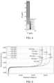
- Figure 4 shows an active charge carrier concentration in an exemplary semiconductor power device that has been simulated using the distribution of the n-type dopant and p-type dopant implantation dosages described in relation to Figure 3(a) .
- the n-type dopant and the p-type dopant concentrations of the first and second pillars, respectively were assumed to be constant in the direction along the first and second pillars, respectively, from drift region to the body region, as described in relation to Figure 3(a) .
- Figure 5 shows a graph of simulated drain source current curves over a breakdown voltage. The curves shown in Figure 5 have been simulated for each of the n-type dopant and p-type dopant implantation dosage distributions described in relation to Figure 3(a) to 3(f) , using the parameters of the device 100 described herein.
- an electric field at the top of the active region 105 may be decreased, leading to a more even distribution of the electric field in the active region 105 of the device 100.
- the effect of decreasing of the electric field at the top of the active region 105 may also be referred to as Reduced Surface Field (RESURF).
- Figure 6 shows a graph of electric field curves over a distance X between the drain contact and the source contact of the device.
- the curves shown in Figure 6 have been simulated for each of the n-type dopant and p-type dopant implantation dosage distributions described in relation to Figure 3(a) to 3(f) , using the parameters of the device 100 described herein.
- the electric field curves simulated for the devices with the n-type dopant and p-type dopant implantation dosage distributions as described in Figures 3(a) and 3(e) are very similar. It can be seen that the electric field simulated for these n-type dopant and p-type dopant implantation dosage distributions decreases towards the drain contact.
- the electric field curves simulated for the devices with the n-type dopant and p-type dopant implantation dosage distributions as described in Figures 3(b) and 3(d) are similar to those for the device with the n-type dopant and p-type dopant implantation dosage distributions as described in Figures 3(a) and 3(e) .
- the electric field curve simulated for the device with the n-type dopant and p-type dopant implantation dosage distribution as described in relation to Figure 3(b) increases in proximity of the drain contact
- the electric field curve simulated for the device with the n-type dopant and p-type dopant implantation dosage distribution as described in relation to Figure 3(d) is decreased in proximity of the drain contact compared to the electric field curves of the other devices.
- the electric field curve simulated for the device with the n-type dopant and p-type dopant implantation dosage distribution as described in relation to Figure 3(c) is decreased in proximity of the source contact compared to the electric field curves of the other devices.
- Figure 7 shows a comparison of the breakdown voltage, specific resistance and Figure of Merit that has been simulated for each of the n-type dopant and p-type dopant implantation dosage distributions as described in Figures 3(a) to 3(f) , using the parameters of the device disclosed herein.
- R sp 2 ⁇ W pitch ⁇ V B ⁇ ⁇ ⁇ S ⁇ E C 2 , where W pitch is the width of the unit cell, V B is the breakdown voltage, ⁇ is the electron mobility, ⁇ S is the permittivity of silicon and E C is the critical electric field. As described above the Figure of Merit corresponds to the ratio V B /R sp .
- the breakdown voltage increases from about 543.7 V for the device with the n-type dopant and p-type dopant implantation dosage distribution as described in Figure 3(a) to 694 V for the device with the n-type dopant and p-type dopant implantation dosage distribution as described in Figure 3(f) .
- the specific resistance increases from 9.6 m ⁇ cm 2 for the device with the n-type dopant and p-type dopant implantation dosage distribution as described in relation to Figure 3(a) to 9.9 m ⁇ cm 2 for the device with the n-type dopant and p-type dopant implantation dosage distribution as described in relation to Figure 3(f) .
- Figure of Merit has increased from 56.6 for the device with the n-type dopant and p-type dopant implantation dosage distribution as described in relation to Figure 3(a) to 70.1 for the device with the n-type dopant and p-type dopant implantation dosage distribution as described in relation to Figure 3(f) .
- Figures 8(a) to 8(f) show simulations of impact ionisation locations 165.
- the impact ionisation locations 165 shown in Figures 8(a) to 8(f) have been simulated for each of the n-type dopant and p-type dopant implantation dosage distributions as described in relation Figures 3(a) to 3(f) , using the parameters of the device 100 described herein.
- the impact ionisation location 165 may be considered as a location at which breakdown occurs.
- the simulated impact ionisation location 165 is at or near the body region 120.
- the impact ionisation location 165 is near a centre of the super junction region 125.
- the impact ionisation location 165 is at the bottom of the super junction region 125.
- the impact ionisation location 165 is proximal to the drift region 115. This may result in an improved non-latch-up performance of the device 100 with the n-type dopant and p-type dopant implantation dosage distribution as described in Figure 3(f) .
- Latch-up may be understood as a creation of a low-impedance path between regions of the device 100 that triggers turn-on of a parasitic n-p-n bipolar transistor structure between the source contact regions 145, the body region 120 and the first pillar 125 or the drain region 115.
- the improved latch-up performance may in turn result in a more even distribution of heat generated in the device 100 compared to the devices with the n-type dopant and p-type dopant implantation dosage distributions as described in relation to Figures 3(a) to 3(e) .
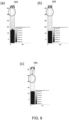
- Figures 9(a) to 9(f) show exemplary n-type dopant and p-type dopant concentrations of the first and second pillars 125a, 125b, respectively, according to embodiments of the present disclosure.
- the concentration of the n-type dopant of the first pillar 125a is constant in the direction X along the first pillar 125a from the drift region 115 to the body region 120.
- the concentration of the p-type dopant of the second pillar decreases in the direction X along the second pillar 125b from the drift region 115 to the body region 120.
- the p-type dopant concentration of the second pillar 125b at or near the body region 120 is less than the n-type dopant concentration of the first pillar 125a, as shown in Figures 9 (a) and 9(c) .
- the p-type dopant concentration of the second pillar 125b at or near the body region 120 is larger than the n-type dopant concentration of the first pillar 125a, as shown in Figures 9 (b) and 9(d) .
- the p-type dopant concentration of the second pillar 125b at or near the body region 120 may be the same as the n-type dopant concentration of the first pillar 125a, as shown in Figure 9(e) and 9(f) .
- the p-type dopant concentration of the second pillar 125b decreases linearly in the direction X along the second pillar 125b from the drift region 115 to the body region 120, as shown in Figures 9(a), 9(b) and (e) .
- the p-type dopant concentration of the second pillar 125b decreases stepwise in the direction X along the second pillar 125b from the drift region 115 to the body region 120, as shown in Figures 9(c), 9(d) and 9(f) .
- the p-type dopant concentration of the second pillar 125b decreases in three steps in the direction X along the second pillar 125b from the drift region 115 to the body region 120.
- p-type dopant concentration may decrease in more than three steps or at least two steps in the direction along the second pillar from the drift region to the body region.
- Figures 10(a) to 10(f) show exemplary n-type dopant and p-type dopant concentrations of the first and second pillars 125a, 125b, respectively, according to embodiments of the present disclosure.
- the concentration of the p-type dopant of the second pillar 125b is constant in the direction X along the second pillar 125b from the drift region 115 to the body region 120.
- the concentration of the n-type dopant of the first pillar 125a increases in the direction X along the first pillar 125a from the drift region 115 to the body region 120.
- the p-type dopant concentration of the second pillar 125b at or near the body region 120 is less than the n-type dopant concentration of the first pillar 125a, as shown in Figures 10 (a) and 10(c) .
- the p-type dopant concentration of the second pillar 125b at or near the body region 120 is larger than the n-type dopant concentration of the first pillar 125a, as shown in Figures 10(b) and 10(d) .
- the p-type dopant concentration of the second pillar 125b at or near the body region 120 may be the same as the n-type dopant concentration of the first pillar 125a, as shown in Figure 10(e) and 10(f) .
- the n-type dopant concentration of the first pillar 125a increases linearly in the direction X along the first pillar 125a from the drift region 115 to the body region 120, as shown in Figures 10(a), 10(b) and 10(e) .
- the n-type dopant concentration of the first pillar 125a increases stepwise in the direction X along the first pillar 125a from the drift region 115 to the body region 120, as shown in Figures 10(c), 10(d) and 10(f) .
- the n-type dopant concentration of the first pillar 125a increases in three steps in the direction X along the first pillar 125a from the drift region 115 to the body region 120.
- n-type dopant concentration may increase in more than three steps or at least two steps in the direction from the drift region to the body region.
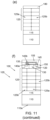
- Figures 11(a) to 11(f) shows steps of a method of manufacturing an active region of a semiconductor power device according to an embodiment of the disclosure, such as the active region 105 of the device 100 described above. Many of the features are the same as those shown in Figures 1 and 2 and therefore carry the same reference numerals. It will be appreciated that the steps shown in Figures 11(a) to 11(f) may illustrate a subset of all the steps for manufacturing a device, and that the method may further include additional steps preceding or following the steps of Figures 11(a) to 11(f) .
- Figures 11(a) to 11(f) show steps in manufacturing an active area having one first pillar 125a and two second pillars 125b, it will be understood that the method may be used to manufacture an active region comprising more than one first pillar and more than two second pillars.
- the method comprises forming the drift region 115 on the substrate 110.
- the drift region 115 may be formed on the substrate 110 using a deposition process.
- the method comprises forming the super junction region 125 on the drift region 115.
- Steps (b) to (c) may each be performed in turn a plurality of times. In the example shown in Figure 11 , the steps (b) and (c) are performed six times. However, it will be appreciated that these steps may be performed more or less than six times.
- the method comprises depositing a semiconductor layer 157 on or over the drift region 115.
- the semiconductor layer 157 may be deposited using a deposition process.
- the method comprises forming a first mask 170 on the semiconductor layer 157.
- the step of forming the first mask 170 on the semiconductor layer 157 may comprise depositing a layer of mask material, such as a layer of resist or photoresist material, on the semiconductor layer 157.
- the step of forming the first mask 170 on the semiconductor layer 157 may comprise patterning the layer of mask material. This may comprise exposing a part of the layer of mask material.
- the step of forming the first mask 170 on the semiconductor layer 157 may comprise developing the layer of mask material.
- a material removal process such as etch process, may be used to remove the exposed part of the layer of mask material, thereby forming the first mask 170.
- the first mask 170 exposes an upper surface of a first region of the semiconductor layer 157.
- the exposed upper surface of the first region of the semiconductor layer 157 may have a width of about 2.6 ⁇ m.
- the exposed upper surface of the first region of the semiconductor layer 157 may also be referred to as an opening of the first mask 170. It will be appreciated that in other embodiments, the width of the exposed upper surface of the first region of the semiconductor layer may be more or less than 2.6 ⁇ m.
- the method comprises is selectively doping the first region of the semiconductor layer 157 by implanting an n-type dopant.
- the n-type dopant may comprise phosphor, arsenic or another n-type dopant.
- the n-type dopant dosage is indicated in Figure 11 by reference numeral 160a.
- the method comprises forming a second mask 175 on the semiconductor layer 157.
- the second mask 175 may be formed in the same manner as the first mask 170.
- the second mask 175 exposes an upper surface of a second region of the semiconductor layer 157.
- the second region of the semiconductor layer 157 is laterally spaced from the first region of the semiconductor layer 157.
- the exposed upper surface of the second region of the semiconductor layer 157 may have a width of about 2.6 ⁇ m.
- the exposed upper surface of the second region of the semiconductor layer 157 may also be referred to as an opening of the second mask 175. It will be appreciated that in other embodiments, the width of the exposed upper surface of the second region of the semiconductor layer may be more or less than 2.6 ⁇ m.
- the method comprises is selectively doping the second region of the semiconductor layer 157 by implanting a p-type dopant.
- the p-type dopant may comprise boron, boron difluoride or another p-type dopant.
- the p-type dopant dosage is indicated in Figure 11 by reference numeral 160b.
- the first and second regions of the semiconductor layer 157 may be implanted using an implantation process, such as vapour diffusion or another implantation process.
- An implantation energy used for implanting the p-type dopant may be between about 100 KeV and 850 KeV.
- An implantation energy used for implanting the n-type dopant in the above examples may be between about 140 KeV and 950 KeV.
- An implantation depth of the n-type and p-type dopants may be between about 0.5 ⁇ m and about 1.7 ⁇ m.
- step (d) the method comprises repeating steps (b) and (c).
- steps (b) and (c) are repeated six times.
- the number of repetitions of step (b) and (c) may be dependent on a required or desired breakdown voltage of the device 100.
- the required or desired breakdown voltage is about 600 V.
- the required or desired breakdown voltage of the device may be more or less than 600 V.
- steps (b) and (c) may be repeated more or less than six times.
- step (b) a subsequent semiconductor layer 157 is deposited on a previously deposited semiconductor layer 157.
- the first mask 170 exposes a same first region of the subsequent semiconductor layer 157 as in one or more previous repetitions of step (b).
- the second mask 175 exposes a same second region of the subsequent semiconductor layer 157 as in one or more previous repetitions of step (c).
- the order of the n-type doing or p-type doing may be changed.
- the p-type dopant dosage may be the same for each semiconductor layer.
- the p-type dopant dosage may be about 1.1 x 10 13 cm -2 .
- the method may comprise forming the first and second pillars 125a, 125b.
- the method may comprise using a diffusion or redistribution process to form the first and second pillars 125a, 125b.
- the diffusion or redistribution process may comprise a drive-in process to further diffuse or redistribute the dopants, thereby forming the first and second pillars 125a, 125b.
- the diffusion or redistribution process may be used to connect the first and second pillars 125a, 125b with each other.
- a diffusion length of the n-type and p-type dopants during the initial vapour diffusion is generally less than a diffusion length of the n-type and p-type dopants during the drive-in process. Therefore, the drive-in process causes the n-type and p-type dopants to diffuse further into the semiconductor layers 157.
- a temperature of the substrate 110, the drift region 115 and the semiconductor layers 157 is increased, e.g. to about 1125°C for about 10 hours.
- the drive-in process causes the n-type and p-type dopants on the surface of the semiconductor layers 157 to be diffused further into the semiconductor layers 157, thereby forming the first and second pillars 125a, 125b. This in turn results in the formation of the super junction region 125.
- the method comprises depositing a further semiconductor layer 180 on the super junction region 125, e.g. using a deposition process.
- the further semiconductor layer 180 may have a thickness of about 2 ⁇ m. However, it will be appreciated that in other embodiments, the further semiconductor layer may he have a thickness of more or less than 2 ⁇ m.
- the further semiconductor layer 180 may also be referred to as a cap layer.
- step (f) the method comprises forming a third mask on the further semiconductor layer 180.
- the third mask exposes a region of the further semiconductor layer 180 above the first pillar 125a.
- the third mask may be formed in the same manner as the first and second masks 170, 175 described above.
- the method comprises forming the JFET region 130.
- the JFET region 130 may be formed by doping the exposed region of the further semiconductor layer 180 with an n-type dopant, e.g. using the implantation process mentioned above.
- the n-type dopant may comprise one or more of the exemplary n-type dopants mentioned above.
- the method further comprises forming the gate oxide region 140a above the JFET region 130.
- the gate oxide region 140a may comprise a thin oxide layer, such as silicon dioxide, that can be deposited or thermally grown.
- the method further comprises forming the gate conductive region 135.
- the method comprises depositing a layer of conductive material on the gate oxide region 140a and over the JFET region 130, e.g. using a deposition process.
- the conductive material may comprise a doped semiconductor material, such as doped polysilicon.
- a material removal process such as a dry-etch or wet-etch process, may be used to form the gate conductive region 135.
- the layer of conductive material may be etched using a mask such that this layer extends over the JFET region 130 to the source contact regions 145.
- the method further comprises forming the body region 120.
- a p-type dopant may be implanted on an upper surface of the further semiconductor layer 180 such that the p-type body region 120 is formed on either side of the JFET region 130.
- the p-type dopant may be implanted using a blank implantation process.
- the diffusion or redistribution process comprising the drive-in process, is performed to further diffuse or redistribute the p-type dopants in the body region 120.
- a temperature of the substrate 110, the drift region 115, super junction region 125 and further semiconductor layer 180 is increased, e.g. to about 1125°C for about 100 minutes.
- the drive-in process causes the p-type dopant on the surface of the further semiconductor layer 180 to be diffused further into the further semiconductor layer 180, thereby forming the body region 120.
- the method further comprises forming the source contact regions 145.
- an n-type dopant may be implanted on either side of the body region 120 to form the source contact regions 145.
- An n-type dopant concentration of each of the source contact regions 145 may be larger than 5 x 10 18 cm -3 .
- the n-type dopant may comprise one or more of the exemplary n-type dopants mentioned above.
- the n-type dopant may be implanted using a blank implantation process.
- the method further comprises forming the interlayer dielectric (ILD) layer 140b.
- the interlayer dielectric layer 140b may be formed by depositing a layer of insulating material on or over the gate conductive region 135, e.g. using a deposition process.
- the layer of insulating material may comprise an oxide material, such as TEOS (tetraethyl orthosilicate).
- the interlayer dielectric layer 140b may also be deposited on or over the gate oxide region 140a.
- the method further comprises forming the p+ contact regions 150.
- the method comprises forming contact openings or recesses, e.g. using a material removal process, e.g. on either side of the gate conductive region 135.
- the contact openings or recesses may be formed by etching through the interlayer dielectric layer 140b and the gate oxide region 140a.
- a p-type dopant may be implanted below each contact opening or recess to form the p + contact regions 150.
- a p-type dopant concentration of the p + contact region 150 may be larger than 5 x 10 18 cm -3 .
- the p-type dopant may comprise one or more of the exemplary p-type dopants mentioned above.
- the p-type dopant may be implanted using a blank implantation process.
- the method further comprises forming the source contact 155.
- the source contact 155 may be formed by depositing a layer of conductive material into each contact opening or recess and on or over the interlayer dielectric layer 140b, e.g. such that the source contact 155 contacts the source contact regions 145 and the p+ contact regions 150.
- the method further comprises forming the drain contact 110a.
- the drain contact 110a may be formed by grinding or planarising a lower surface of the substrate 110 and depositing a layer of conductive material thereon.
- the layer of conductive material may be deposited on the lower surface of the substrate 110 using a deposition process, such as an evaporation process.
- Figures 12(a) to 12(k) shows steps of another method of manufacturing an active region of a semiconductor power device according to an embodiment of the disclosure, such as the active region 105 of the device 100 described above. Many of the features are the same as those shown in Figures 1 and 2 and therefore carry the same reference numerals. It will be appreciated that the steps shown in Figures 12(a) to 12(k) may illustrate a subset of all the steps for manufacturing a device, and that the method may further include additional steps preceding or following the steps of Figures 12(a) to 12(k) .
- the semiconductor region 185 includes one or more epitaxial layers that have been formed on the substrate 110.
- a thickness T of the semiconductor region 185 may be about 50 ⁇ m.
- the thickness of the semiconductor region 185 may be dependent on the required or desired breakdown voltage of the device 100. In the embodiments shown herein the required or desired breakdown voltage is about 600 V. However, it will be appreciated that in other embodiments, the required or desired breakdown voltage of the device may be more or less than 600 V. In such other embodiments, the thickness of the semiconductor region may be more or less than 50 ⁇ m.
- the method comprises forming the JFET region 130.
- the step of forming the JFET region 130 may comprise forming a fourth mask 190 on the semiconductor region 185.
- the fourth mask exposes an upper surface of a first region of the semiconductor region 185.
- the fourth mask may be formed in the same manner as the first and second masks 170, 175 described above.
- the JFET region 130 may be formed by doping the first region of the semiconductor region 185 with an n-type dopant, e.g. using the implantation process mentioned above.
- the n-type dopant may comprise one or more of the exemplary n-type dopants mentioned above.
- the method comprises forming the body region 120.
- the step of forming the body region 120 may comprise forming a fifth mask on the semiconductor region 185.
- the fifth mask exposes an upper surface of a second region of the semiconductor region 185.
- the second region of the semiconductor region 185 is located adjacent the JFET region 130.
- the fifth mask may be formed in the same manner as the first and second masks 170, 175 described above.
- the body region 120 may be formed by doping the second region of the semiconductor region 185 with a p-type dopant.
- the p-type dopant may be implanted using a blank implantation process.
- the diffusion or redistribution process comprising the drive-in process, is performed to further diffuse or redistribute the p-type dopants in the body region 120.
- a temperature of the substrate 110 and the semiconductor region 185 is increased, e.g. to about 1125°C for about 100 minutes.
- the drive-in process causes the p-type dopant on the surface of the semiconductor region 185 to be diffused further into the semiconductor region 185, thereby forming the body region 120.
- the method comprises depositing a layer of mask material 195 on the upper surface of the semiconductor region 185, e.g. over the JFET region 130 and the body region 120.
- the layer of mask material 195 comprises a stack of a layer of nitride material 195a sandwiched between two layers of oxide material 195b.
- the nitride material may comprise silicon nitride, such as such as Si 3 N 4 or the like.
- the oxide material may comprise TEOS (tetraethyl orthosilicate) or the like.
- the layer of mask material 195 may be patterned, e.g. using a material removal process, such as a dry-etch process or a wet-etch process.
- the method comprises forming a trench 200 in the semiconductor region 185.
- the trench 200 is formed such that it extends through the body region 120 into semiconductor region 185.
- the trench 200 extends into the semiconductor region 185 in a vertical direction (e.g. a direction that is perpendicular to the substrate 110).
- the trench 200 is in contact with the body region 120.
- the trench 200 may be formed using a material removal process, such as a dry-etch process.
- the patterned layer of mask material may act as a hard mask or resists layer to define the trench 200 during the material removal process.
- the trench 200 may comprise a height H of about 35 ⁇ m.
- the trench 200 may comprise a width of about 5 ⁇ m.
- the width of the trench 200 is indicated by reference numeral W/2.
- the sidewalls of the trench 200 may be formed at an angle ⁇ relative to a surface of the substrate 110.
- the angle ⁇ may be between about 80 degrees and about 90 degrees, such as about 88 degrees.
- a portion of the semiconductor region 185 below the trench 200 may define the drift region 115.
- the trench 200 is also in contact with the drift region 115. It will be appreciated that in other embodiments, a height and/or width of trench may be different from the exemplary height and/or width disclosed herein.
- a portion of the layer of mask material 195 may be removed, e.g. using a material removal process, such as a wet-etch process.
- a material removal process such as a wet-etch process.
- the upper of the two layers of oxide material 195b and the layer of nitride material 195a are removed.
- the lower of two layers of oxide material 195b remains on the upper surface of the semiconductor region 185, e.g. on the body region 120 and the JFET region 130.
- the method further comprises filling the trench 200 with a p-type semiconductor material 205, such as p-type doped silicon.
- the trench 200 may be filled with the semiconductor material 205 using a deposition process.
- the semiconductor material 205 may be doped such that a doping concentration of the semiconductor material 205 in the trench 200 decreases in a direction along the trench 200 from the drift region 115 to the body region 120.
- the p-type doping concentration of the semiconductor material 205 in the trench 200 may decrease from about 7.35 x 10 15 cm -3 to 6.9 x 10 15 cm -3 in the direction along the trench 200 from the drift region 115 to the body region 120.
- the direction along the trench 200 may also be understood as a vertical direction, e.g.
- the trench 200 forms the second pillar 125b.
- a portion of the semiconductor region 185 that is located adjacent to the trench 200 forms the first pillar 125a.
- a doping concentration of the first pillar 125a is constant in the direction along the first pillar from the drift region 115 to the body region 120.
- an n-type doping concentration of the first pillar 125a may be about 7 x 10 15 cm -3 .
- a doping concentration of the first pillar may increases in the direction along the first pillar from the drift region to the body region and a doping concentration of the second pillar or portion thereof may be constant in the direction along the second pillar from the drift region to the body region.
- the p-type doping concentration of the second pillar or portion thereof may be about 7 x 10 15 cm -3 .
- the n-type doping concentration of the first pillar may increase from about 6.65 x 10 15 cm -3 to about 7.2 x 10 15 cm -3 in the direction along the first pillar from the drift region 115 to the body region 120.
- the body region 120 is located on a part of the super junction region 125, e.g. on at least a part of the first pillar 125a.
- the super junction region 125 can be considered as being arranged at least partially between the drift region 115 and the body region 120.
- step (f) the method further comprises removing a portion of the semiconductor material 205 that extends beyond the body region 120 and the JFET region 130, e.g. using a material removal process, such as a dry-etch process or chemical-mechanical polishing process.
- a material removal process such as a dry-etch process or chemical-mechanical polishing process.
- the method comprises removing a remainder of the layer of mask material 195, e.g. the lower of two layers of oxide material 195b.
- the remainder of the layer of mask material 195 may be removed using a material removal process, such as a wet-etch process.
- a sacrificial layer of oxide material may be deposited on the JFET region 130, the body region 120 and the second pillar 125b. The sacrificial layer of oxide material may subsequently be removed.
- step (h) the method comprises depositing a layer of oxide material 210, such as silicon dioxide, on the JFET region 130, the body region 120 and the second pillar 125b.
- oxide material 210 such as silicon dioxide
- the method further comprises forming the gate conductive region 135.
- the method comprises depositing a layer of conductive material on the layer of oxide material 210.
- the conductive material may comprise a doped semiconductor material, such as doped polysilicon.
- a material removal process such as a dry-etch or wet-etch process, may be used to form the gate conductive region 135.
- the layer of conductive material may be etched using a mask such that this layer extends over the JFET region 130 and the body region 120. A portion of the layer of oxide material 210 that is located over the second pillar 125b is exposed.
- step (i) the method comprises partially removing the exposed portion of the layer of oxide material 210 using a material removal process, such as a dry-etch or wet-etch process.
- a material removal process such as a dry-etch or wet-etch process.
- the method further comprises forming the source contact region 145.
- an n-type dopant is implanted in a region of the second pillar 125b adjacent to the body region 120 to form the source contact regions 145.
- the region of the second pillar 125b that is implanted with the n-type dopant is located below the layer of oxide material 210 and extends from the exposed portion of the layer of oxide material 210 to the gate conductive region 135.
- a sixth mask exposes the region of the second pillar 125b to be implanted.
- An n-type dopant concentration of the source contact region 145 may be larger than 5 x 10 18 cm -3 .
- the n-type dopant may comprise one or more of the exemplary n-type dopants mentioned above.
- the n-type dopant may be implanted using a blank implantation process.
- the diffusion or redistribution process comprising the drive-in process, is performed to further diffuse or redistribute the n-type dopants in the region of the second pillar 125b.
- a temperature of at least the second pillar 125b is increased, e.g. to about 1000°C for about 30 minutes.
- the drive-in process causes the n-type dopant on the surface of the region of the second pillar 125b to be diffused further into this region, thereby forming the source contact region 145.
- the method comprises forming the interlayer dielectric layer 140b.
- the interlayer dielectric layer 140b may be formed by depositing a layer of insulating material on or over the gate conductive region 135 and the exposed portion of the layer of oxide material 210, e.g. using a deposition process.
- the layer of insulating material may comprise an oxide material, such as TEOS (tetraethyl orthosilicate).
- the method further comprises forming the p+ contact region 150.
- the method comprises forming an opening or recess, e.g. using a material removal process.
- the opening or recess is laterally spaced from the gate conductive region 135.
- the contact opening or recess may be formed by etching through the interlayer dielectric layer 140b and the layer of oxide material 210. The remainder of the layer of oxide material 210 forms the gate oxide region 140a.
- a p-type dopant may be implanted below the contact opening or recess to form the p + contact region 150.
- a p-type dopant concentration of the p + contact region 150 may be larger than 5x 10 18 cm -3 .
- the p-type dopant may comprise one or more of the exemplary p-type dopants mentioned above.
- the p-type dopant may be implanted using a blank implantation process.
- the method further comprises forming the source contact 155.
- the source contact 155 may be formed by depositing a layer of conductive material into the contact opening or recess and on or over the interlayer dielectric layer 140b, e.g. such that the source contact 155 contacts the source contact region 145 and the p+ contact region 150.
- the method further comprises forming the drain contact 110a.
- the drain contact 110a may be formed by grinding or planarising a lower surface of the substrate 110 and depositing a layer of conductive material thereon.
- the layer of conductive material may be deposited on the lower surface of the substrate 110 using a deposition process, such as an evaporation process.
- Figure 13 shows schematically a cross-section of a super junction region 125 that has been formed using one or more steps of the method described in relation to Figures 12(a) to 12(k) .
- the super junction region 125 comprises a second pillar 125b that is arranged between two portions of two first pillars 125a.
- the device 100 may more than one second pillar 125b and more than two first pillars 125a, as mentioned above.
- the deposition process described above may comprise a chemical vapour deposition process, sputtering process or another deposition process.
- the dry-etch process mentioned above may include a reactive ion etch process or another dry-etch process.
- width encompasses a size, dimension or extension of a part or feature in a lateral direction, e.g. a direction parallel to the y-axis in Figure 4 .
- thickness or “height” used herein encompasses a size, dimension or extension of a part or feature in a longitudinal or vertical direction, e.g. a direction parallel to the x-axis in Figure 4 and/or a direction perpendicular to the lateral direction.
- the device may comprise an insulated-gate bipolar transistor (IGBT). Any of the above-mentioned features may also apply to the IGBT.
- the terms “drain region” may be replaced with the terms “collector region” and the term “source”, as used above, may be replaced with the term “emitter”.
- Figures 1 to 3(f) , 11(a) to 11(f) , 12(a) to 12(k) and 13 are schematic drawings of some embodiments of the disclosure and may not be to scale.
Landscapes
- Insulated Gate Type Field-Effect Transistor (AREA)
Abstract
A semiconductor power device comprising an active region, the active region comprising a drift region of a first conductivity type, a body region of a second conductivity type, wherein the second conductivity type is opposite to the first conductivity type, a super junction region arranged at least partially between the drift region and the body region, the super junction region comprising a first pillar of the first conductivity type, at least a portion of a second pillar of the second conductivity type, the first pillar being arranged adjacent to the portion of the second pillar, wherein at least one of: a doping concentration of the first pillar is constant in a direction along the first pillar from the drift region to the body region and a doping concentration of the portion of the second pillar decreases in a direction along the portion of the second pillar from the drift region to the body region, or the doping concentration of the first pillar increases in the direction along the first pillar from the drift region to the body region and the doping concentration of the portion of the second pillar is constant in the direction along the portion of the second pillar from the drift region to the body region.
Description
- The present disclosure relates to a power semiconductor device and a method of manufacturing a power semiconductor device. Particularly but not exclusively, the present disclosure relates to a super junction (SJ) metal-oxide semiconductor field-effect transistor (MOSFET).
- Power semiconductor devices such as metal-oxide semiconductor field-effect transistors (MOSFETs) or insulated-gate bipolar transistors (IGBTs) require a high breakdown voltage. It is possible to achieve a high value of breakdown voltage in the active regions of super junction MOSFETS, for example by using a number of thin semiconductor layers in the super junction area to create charge balance. However, it can be difficult to improve the Figure of Merit (FOM), which corresponds to a ratio of the breakdown voltage over the specific resistance of a super junction MOSFET, when a cell pitch is decreased. For example, when the cell pitch is decreased, a doping concentration in the super junction region of the MOSFET may be increased to decrease the specific resistance. However, this can also lead to a decrease of the breakdown voltage, which may be due to an increased electric field at a top portion of the super junction region compared to an electric field at a bottom portion of the super junction region.
-
US 9,595,596 B2 US 9,024,381 B2 US6630698B1 relates to a high-voltage semiconductor component andUS 8,283,720 B2 relates to power semiconductor device. - Aspects and preferred features are set out in the accompanying claims.
- According to a first aspect of the present disclosure, there is provided a semiconductor power device comprising an active region, the active region comprising:
- a drift region of a first conductivity type;
- a body region of a second conductivity type, wherein the second conductivity type is opposite to the first conductivity type;
- a super junction region arranged at least partially between the drift region and the body region, the super junction region comprising:
- a first pillar of the first conductivity type,
- at least a portion of a second pillar of the second conductivity type, the first pillar being arranged adjacent to the portion of the second pillar, wherein at least one of:
- a doping concentration of the first pillar is constant in a direction along the first pillar from the drift region to the body region and a doping concentration of the portion of the second pillar decreases in a direction along the portion of the second pillar from the drift region to the body region; or
- the doping concentration of the first pillar increases in the direction along the first pillar from the drift region to the body region and the doping concentration of the portion of the second pillar is constant in the direction along the portion of the second pillar from the drift region to the body region.
- By configuring a doping concentration of the first pillar to be constant in a direction along the first pillar from the drift region to the body region and a doping concentration of the portion of the second pillar to decrease in a direction along the portion of the second pillar from the drift region to the body region, or the doping concentration of the first pillar to increase in the direction along the first pillar from the drift region to the body region and the doping concentration of the portion of the second pillar to be constant in the direction along the portion of the second pillar from the drift region to the body region, a breakdown voltage of the device may be increased. This in turn may lead to an increase in a ratio of the breakdown voltage over a specific resistance of the device. This ratio may also be referred to the Figure of Merit (FOM).
- Additionally, an electric field at a top or a surface of the active region may be decreased. This may lead to a more even distribution of the electric field in the active region of the device. The effect of decreasing of the electric field at the top or surface of the active region may also be referred to as Reduced Surface Field (RESURF).
- Additionally, an impact ionisation location of the device may be located at a bottom of the super junction region, e.g. proximal to the drift region. This may result in an improved non-latch-up performance of the device. The improved latch-up performance may in turn result in a more even distribution of heat generated in the device.
- The doping concentration of the portion of the second pillar may decrease linearly in the direction along the portion of the second pillar from the drift region to the body region. Alternatively, the doping concentration of the first pillar may increase linearly in the direction along the first pillar from the drift region to the body region.
- The doping concentration of the portion of the second pillar may decrease stepwise in the direction along the portion of the second pillar from the drift region to the body region. Alternatively, the doping concentration of the first pillar may increase stepwise in the direction along the first pillar from the drift region to the body region.
- The doping concentration of the portion of the second pillar may decrease in two or more steps. Alternatively, the doping concentration of the first pillar may increase in two or more steps.
- The doping concentration of the first pillar at or near the body region may be larger, smaller or the same as the doping concentration of the portion of the second pillar at or near the body region.
- The super junction region may comprises a plurality of first pillars and a plurality of second pillars. The plurality of first pillars and the plurality of second pillars may be alternately arranged with each other. The portion of the second pillar may be part of or comprised in at least one second pillar of the plurality of second pillars. Each of the plurality of first pillars may arranged adjacent at least one of the plurality of second pillars. Each of the plurality of first pillars may form a p-n-junction with the at least one of the plurality of second pillars.
- The semiconductor device may comprise a metal-oxide-semiconductor field-effect transistor (MOSFET) or an insulated-gate bipolar transistor (IGBT).
- The first pillar or each of the plurality of first pillars may comprise or define a further drift region. The portion of the second pillar, the second pillar or each of the plurality of second pillars may comprise or define a partition region.
- According to a second aspect of the present disclosure there is provided a method of manufacturing an active region of a semiconductor power device, the method comprising:
- forming a drift region of a first conductivity type on a substrate;
- forming a super junction region on the drift region, the super junction region comprising:
- a first pillar of the first conductivity type,
- at least a portion of a second pillar of the second conductivity type, the first pillar being arranged adjacent to the portion of the second pillar, wherein at least one of:
- a doping concentration of the first pillar is constant in a direction along the first pillar from the drift region to the body region and a doping concentration of the portion of the second pillar decreases in a direction along the portion of the second pillar from the drift region to the body region; or
- the doping concentration of the first pillar increases in the direction along the first pillar from the drift region to the body region and the doping concentration of the portion of the second pillar is constant in the direction along the portion of the second pillar from the drift region to the body region;
- forming a body region of a second conductivity type on at least a part of the super junction region.
- Forming the super junction region may comprise:
performing each of steps (i) to (v) one or more times: - (i) depositing a semiconductor layer on or over the drift region;
- (ii) forming a first mask on the semiconductor layer, the first mask exposing an upper surface of a first region of the semiconductor layer;
- (iii) selectively doping the first region of the semiconductor layer to form a first region of a first conductivity type;
- (iv) forming a second mask on the semiconductor layer, the second mask exposing an upper surface of a second region of the semiconductor layer, the second region of the semiconductor layer being laterally spaced from the first region of the semiconductor layer; and
- (v) selectively doping the second region of the semiconductor layer to form a second region of a second conductivity type.
- In a first iteration, the semiconductor layer may be deposited on the drift region. In one or more subsequent iterations, a subsequent semiconductor layer may be deposited on a previously deposited semiconductor layer.
- When at least one subsequent iteration has been performed, a doping concentration of each first region of the first conductivity type may be the same. When at least one subsequent iteration has been performed, a doping concentration of a second region of the second conductivity type formed in the at least one subsequent iteration may be decreased relative to a doping concentration of a second region of the second conductivity type formed in a previous iteration.
- When at least one subsequent iteration has been performed, a doping concentration of each second region of the second conductivity type may be the same. When at least one subsequent iteration has been performed, a doping concentration of a first region of the first conductivity type formed in the at least one subsequent iteration may be increased relative to a doping concentration of a first region of the first conductivity type formed in a previous iteration.
- The method may comprise using a diffusion or redistribution process to form the first pillar and at least the portion of the second pillar.
- Forming the super junction region may comprise forming a trench in a semiconductor region of a first conductivity type. The method may comprise forming the body region prior to forming the trench. The trench may be formed such that the trench extends through the body region into semiconductor region. The trench may extend into the semiconductor region in a vertical direction. The trench may be formed such that the trench is in contact with the body region. The trench may be formed such that the trench is in contact with the drift region.
- A portion of the semiconductor region that is located adjacent to the trench may form the first pillar. Forming the super junction region may comprise filling the trench with a semiconductor material of a second conductivity type to form at least the portion of the second pillar.
- According to a third aspect of the present disclosure there is provided a method of manufacturing a semiconductor power device comprising manufacturing an active region of the semiconductor power device according to the second aspect.
- The device and method of manufacture of the present disclosure has one or more of the following advantages over state-of-the-art devices:
- The device may have an increased breakdown voltage and increased Figure of Merit;
- A distribution of an electric field in the active region may be improved;
- The Reduced Surface Field (RESURF) effect may be improved;
- A non-latch-up performance of the device may be improved;
- A distribution of heat generated in the active region of the device may be more even;
- The manufacturing steps may be compatible with existing MOSFET and/or IGBT manufacturing processes and/or may be performed using materials and processing equipment commonly available in MOSFET and/or IGBT fabs.
- Some embodiments of the disclosure will now be described, by way of example only and with reference to the accompanying drawings, in which:
-
Figure 1 shows schematically a cross-section of an active region of a semiconductor device; -
Figure 2 shows schematically a cross-section of a half of a unit cell of the device ofFigure 1 ; -
Figures 3(a) to 3(f) show schematically different exemplary distributions of dopant dosages that may be used to form a first pillar and a second pillar of the device ofFigures 1 and 2 ; -
Figure 4 shows an active charge carrier concentration in an exemplary semiconductor power device that has been simulated using the distribution of the n-type dopant and p-type dopant implantation dosages ofFigure 3(a) ; -
Figure 5 shows a graph of drain source current curves over a breakdown voltage that have been simulated for each of the n-type dopant and p-type dopant implantation dosage distributions ofFigure 3(a) to 3(f) ; -
Figure 6 shows a graph of electric field curves over a distance between a drain contact and a source contact of the device ofFigures 1 and 2 that have been simulated for each of the n-type dopant and p-type dopant implantation dosage distributions ofFigure 3(a) to 3(f) ; -
Figure 7 shows a comparison between the breakdown voltage, specific resistance and Figure of Merit that has been simulated for each of the n-type dopant and p-type dopant implantation dosage distributions ofFigures 3(a) to 3(f) ; -
Figures 8(a) to 8(f) show simulations of impact ionisation locations that have been simulated for each of the n-type dopant and p-type dopant implantation dosage distributions ofFigures 3(a) to 3(f) ; -
Figures 9(a) to 9(f) show exemplary n- type dopant and p-type dopant concentrations of the first and second pillars, respectively, of the device ofFigures 1 and 2 according to embodiments of the present disclosure; -
Figures 10(a) to 10(f) show exemplary n-type dopant and p-type dopant concentrations of the first and second pillars, respectively, of the device ofFigures 1 and 2 according to embodiments of the present disclosure; -
Figures 11(a) to 11(f) shows steps of a method of manufacturing an active region of a semiconductor power device according to an embodiment of the disclosure; -
Figures 12(a) to 12(k) shows steps of another method of manufacturing an active region of a semiconductor power device according to an embodiment of the disclosure; and -
Figure 13 shows schematically a cross-section of a super junction region that has been formed using one or more steps of the method ofFigures 12(a) to 12(k) . -
Figures 1 and 2 show schematically a cross-section of anactive region 105 of asemiconductor device 100. Theactive region 105 shown inFigure 1 may be considered as a unit cell, which may be repeated thousands of times in thedevice 100. Theactive region 105 shown inFigure 2 may be considered as a half of the unit cell shown inFigure 1 . In the examples described herein, thedevice 100 is a silicon based super junction MOSFET. However, it will be appreciated that the device may comprise one or more alternative semiconductor materials. For example, the device may alternatively be silicon carbide (SiC) or Gallium Nitride (GaN) based. - The
active region 105 comprises asubstrate 110 of a first conductivity type. Thesubstrate 110 may comprise an n-type doped semiconductor material, such as n+ silicon. An n-type dopant concentration of thesubstrate 110 may be larger than about 5 x 1018 cm-3. Thesubstrate 110 is conductive and acts as a drain region. A thickness of the substrate may be between about 40 µm and about 100 µm. - The
active region 105 comprises adrift region 115 arranged on thesubstrate 110. Thedrift region 115 comprises an n-type doped semiconductor material, such as n-type doped silicon. An n-type dopant concentration of thedrift region 115 may be between about 5 x 1014 cm-3 and 5 x 1017 cm-3, such as about 7 x 1015 cm-3. Thedrift region 115 may also be referred to as an n-drift region, n-type buffer region or n-type voltage sustaining region. Thedrift region 115 is formed on or over thesemiconductor substrate 110. In this embodiment, thedrift region 115 comprises one or more epitaxial layers and has a thickness of about 15 µm. However, it will be appreciated that in other embodiments, the drift region may have a thickness that is more or less than 15 µm. - A
drain contact 110a may be arranged on an underside of thesubstrate 110, e.g. a side of thesubstrate 110 that is opposite to thedrift region 110. Thedrain contact 110a may comprise a conductive material, such as a metal material. The metal material may comprise a metal alloy, such as titanium nickel silver or another metal alloy. - The
active area 105 includes abody region 120 of a second conductivity type. The second conductivity type is opposite to the first conductivity type. In the embodiment shown inFigures 1 and 2 , thebody region 120 comprises a p-type semiconductor material. - The
active area 105 includes asuper junction region 125. Thesuper junction region 125 is arranged between thedrift region 115 and thebody region 120. Thesuper junction region 125 comprises a plurality offirst pillars 125a of the first conductivity type and a plurality ofsecond pillars 125b of the second conductivity type. In this embodiment, eachfirst pillar 125a is an n-type pillar and eachsecond pillar 125b is a p-type pillar. Thefirst pillars 125a may define further drift regions. Thesecond pillars 125b may define partition regions. The first andsecond pillars first pillar 125a is arranged between two adjacentsecond pillars 125b. For example, in the unit cell shown inFigure 1 , thesuper junction region 125 comprises afirst pillar 125a and two portions of two respectivesecond pillars 125b. Thefirst pillar 125a is arranged between the two portions thesecond pillars 125b. In the half of the unit cell shownFigure 2 , the super junction region comprises a portion of thefirst pillar 125a and a portion of thesecond pillar 125b. The portions of the first andsecond pillars drift region 115 and thebody region 120. Thesuper junction region 125 may also be referred to as a p-n-junction region. - In this embodiment, a width of each of the first and
second pillars second pillars - The
active region 105 comprises an n-type dopedJFET region 130. The JFET region is arranged above thefirst pillar 125a. TheJFET region 130 is arranged to extend from the first pillar to an upper surface of thebody region 120. Thebody region 120 is arranged on either side of theJFET region 130. - The
active region 105 comprises a gateconductive region 135. The gateconductive region 135 is located above theJFET region 130 and thebody region 120. The gateconductive region 135 is used to control a conduction channel in theactive region 105. - The
active region 105 comprises afirst insulation region 140a. Thefirst insulation region 140a is arranged between theJFET region 130 and the gateconductive region 135. Thefirst insulation region 140a may extend along the sides of the gateconductive region 135. The first insulation region may be referred to as agate oxide region 140a. - The
active region 105 comprises asecond insulation region 140b. Thesecond insulation region 140b is arranged on or over the gateconductive region 135 and thegate oxide region 140a. The second insulation region may also be referred to as aninterlayer dielectric layer 140b. - The
device 100 includes source contact regions, which in this example are n+source contact regions 145. The n+source contact regions 145 are arranged on either side of theJFET region 130 and below thegate oxide region 140a. During operation, a conduction channel is formed between the n+source contact regions 145 and thedrift region 115 by application of a positive voltage to the gateconductive region 135. - The
body region 120 comprises a contact region, which in this example comprises p+ contact regions 150. The p+ contact regions 150 are formed on either side of theJFET region 130 and adjacent a respective n+ source contact 145 region. - The
device 100 comprises asource contact 155. Thesource contact 155 may comprise a conductive material, such as a metal material. The metal material may comprise aluminium, tungsten, titanium or a combination thereof. Thesource contact 155 is located on an upper surface of the device. For example, thesource contact 155 may be arranged on or over theinterlayer dielectric layer 140b. Thesource contact 155 may also be arranged to contact the n+ source contact 145 regions and the p+ contact regions 150. - In the embodiments shown in
Figure 1 , a lateral extension or a width of the unit cell of thedevice 100 is about 7 µm. However, it will be appreciated that in other embodiments, the lateral extension or cell pitch may be more or less than 7 µm. The lateral extension or the width of the unit cell of the device may also be referred to as cell pitch. -
Figures 3(a) to 3(f) show schematically different exemplary distributions of dopant dosages that may be used to form the first andsecond pillars second pillars Figures 3(a) to 3(f) byreference numeral 157. The semiconductor layers 157 may also be referred to as epitaxial layers. Each of the semiconductor layers may have a thickness of about 6 µm. However, it will be appreciated that in other embodiments, a thickness of each semiconductor layer may be more or less than 6 µm. - The n-type dopant dosage is indicated by
reference numeral 160a and the p-type dopant dosage is indicated byreference numeral 160b. For sake of clarity only thedrift region 115 and thebody region 120 are indicated inFigures 3(a) to 3(f) . - In the examples shown in
Figures 3(a) to 3(f) , the first andsecond pillars - In the example shown in
Figure 3(a) , each of the semiconductor layers 157 is implanted with the same dosage of the p-type dopant and n-type dopant. For example, the p-type dopant 160b and the n-type dopant 160a implantation dosages may be about 1.1 x 1013 cm-2. - As such, a doping concentration of each of the first and
second pillars second pillars drift region 115 to thebody region 120. The terms "a direction along the first/second pillar" may be understood as encompassing the terms "a direction parallel to a longitudinal axis of the first/second pillar." The direction along the first/second pillar may also be referred to as a vertical direction. - In the example shown In
Figure 3(b) , a p-type dopant dosage 160b of thesemiconductor layer 157 adjacent thedrift region 115 is higher relative to the p-type dopant of the remaining semiconductor layers 157. As such, a p-typedopant enrichment region 160c is formed in thesecond pillar 125b in proximity of thedrift region 115. For example, the p-type dopant dosage of theenrichment region 160c is about 1.2 x 1013 cm-2. The p-type dopant dosage of each of the remaining semiconductor layers 157 may be about 1.1 x 1013 cm-2. The n-type dopant dosage 160a is the same for eachsemiconductor layer 157. For example, the n-type dopant dosage is about 1.1 x 1013 cm-2 for eachsemiconductor layer 157. The doping concentration of thefirst pillar 125a is constant in the direction along thefirst pillar 125a from thedrift region 115 to thebody region 120. In the example shown inFigure 3(c) , the p-type dopant dosage 160b is varied across the semiconductor layers 157 in the direction from thedrift region 115 to thebody region 120. In this example, the p-type dopant dosage gradually decreases and then gradually increases in the direction from thedrift region 115 to thebody region 120. For example, the p-type dosage decreases from about 1.16 x 1013 cm-2 to about 1.11 x 1013 cm-2 and then increases from about 1.11 x 1013 cm-2 to about 1.16 x 1013 cm-2. The n-type dopant dosage 160a is the same for eachsemiconductor layer 157. For example, the n-type dopant dosage 160a is about 1.1 x 1013 cm-2 for eachsemiconductor layer 157. - In the example shown in
Figure 3(d) , the p-type dopant dosage 160b is varied across the semiconductor layers 157 in the direction from thedrift region 115 to thebody region 120. In this example, the p-type dopant dosage 160b gradually increases in the direction from thedrift region 115 to thebody region 120. For example, the p-type dosage increases from about 1.07 x 1013 cm-2 to about 1.12 x 1013 cm-2. The n-type dopant dosage 160a is the same for eachsemiconductor layer 157. For example, the n-type dopant dosage 160a is about 1.1 x 1013 cm-2 for eachsemiconductor layer 157. - In the example shown in
Figure 3(e) , the n-type dopant and p-type dopant dosages drift region 115 to thebody region 120. In this example, the n-type dopant and p-type dopant dosages drift region 115 to thebody region 120. For example, the n-type dopant and p-type dopant dosages -
Figure 3(f) shows the n-type dopant and p-typedopant implanting dosages Figure 3(f) , the p-type dopant dosage 160b is varied across the semiconductor layers 157 in the direction from thedrift region 115 to thebody region 120. For example, the p-type dopant dosage 160b decreases in the direction from thedrift region 115 to thebody region 120. The p-type dopant dosage 160b may decrease from about 1.16 x 1013 cm-2 to about 1.09 x 1013 cm-2. - The n-
type dopant dosage 160a is the same for eachsemiconductor layer 157. The n-type dopant dosage may be about 1.1 x 1013 cm-2. It will be appreciated that in other embodiments, the n-type dopant dosage may be varied across the semiconductor layers and the p-type dopant dosage may be constant. In such other embodiments, the n-type dopant dosage may be increased, e.g. from about 1.05 x 1013 cm-2 to 1.11 x 1013 cm-2, in the direction from the drift region to the body region. In such other embodiments, the p-type dopant dosage may be the same for each semiconductor layer. For example, the p-type dopant dosage may be about 1.1 x 1013 cm-2. - An implantation energy used for implanting the p-type dopant in the above examples may be between about 100 KeV and 850 KeV. An implantation energy used for implanting the n-type dopant in the above examples may be between about 140 KeV and 950 KeV.
-
Figure 4 shows an active charge carrier concentration in an exemplary semiconductor power device that has been simulated using the distribution of the n-type dopant and p-type dopant implantation dosages described in relation toFigure 3(a) . In other words, the n-type dopant and the p-type dopant concentrations of the first and second pillars, respectively, were assumed to be constant in the direction along the first and second pillars, respectively, from drift region to the body region, as described in relation toFigure 3(a) . -
Figure 5 shows a graph of simulated drain source current curves over a breakdown voltage. The curves shown inFigure 5 have been simulated for each of the n-type dopant and p-type dopant implantation dosage distributions described in relation toFigure 3(a) to 3(f) , using the parameters of thedevice 100 described herein. - It can be seen from
Figure 5 that the highest breakdown voltage has been simulated for thedevice 100 with n-type dopant and p-type dopant implantation dosages as described in theFigure 3(f) . In other words, by configuring thedevice 100 with afirst pillar 125a having a constant n-type dopant concentration in the direction along thefirst pillar 125a from thedrift region 115 to thebody region 120 and at least a portion of asecond pillar 125b having a p-type dopant concentration that decreases in the direction along the second apillar 125b from thedrift region 115 to thebody region 120, a breakdown voltage of thedevice 100 may be increased. This in turn leads to an increase in a ratio of the breakdown voltage over a specific resistance of thedevice 100. This ratio may also be referred to the Figure of Merit (FOM). - Additionally, by configuring the
device 100 with afirst pillar 125a having a constant n-type dopant concentration in the direction along thefirst pillar 125a from thedrift region 115 to thebody region 120 and at least a portion of asecond pillar 125b having a p-type dopant concentration that decreases in the direction along thesecond pillar 125b from thedrift region 115 to thebody region 120, an electric field at the top of theactive region 105 may be decreased, leading to a more even distribution of the electric field in theactive region 105 of thedevice 100. The effect of decreasing of the electric field at the top of theactive region 105 may also be referred to as Reduced Surface Field (RESURF). -
Figure 6 shows a graph of electric field curves over a distance X between the drain contact and the source contact of the device. The curves shown inFigure 6 have been simulated for each of the n-type dopant and p-type dopant implantation dosage distributions described in relation toFigure 3(a) to 3(f) , using the parameters of thedevice 100 described herein. It can be seen fromFigure 6 that the electric field is more evenly distributed between thesource contact 155 and thedrain contact 110a for thedevice 100 with n-type dopant and p-type dopant implantation dosages as described inFigure 3(f) compared to electric field curves simulated for the devices with the n-type dopant and p-type dopant implantation dosage distributions described in relation toFigure 3(a) to 3(e) . In addition, it can be seen fromFigure 6 that the electric field is decreased in proximity of thesource contact 155 for thedevice 100 with n-type dopant and p-type dopant implantation dosages as described in theFigure 3(f) compared to electric field curves simulated for the devices with the n-type dopant and p-type dopant implantation dosage distributions described in relation toFigure 3(a), 3(b), 3(d) and 3(e) . Although the simulated electric field for the devices with the n-type dopant and p-type dopant implantation dosage distributions described in relation toFigure 3(c) is decreased in proximity at the source contact, it is less even in the remainder of the active region compared to the electric field simulated for thedevice 100 with n-type dopant and p-type dopant implantation dosages as described in theFigure 3(f) . - The electric field curves simulated for the devices with the n-type dopant and p-type dopant implantation dosage distributions as described in
Figures 3(a) and 3(e) are very similar. It can be seen that the electric field simulated for these n-type dopant and p-type dopant implantation dosage distributions decreases towards the drain contact. The electric field curves simulated for the devices with the n-type dopant and p-type dopant implantation dosage distributions as described inFigures 3(b) and 3(d) are similar to those for the device with the n-type dopant and p-type dopant implantation dosage distributions as described inFigures 3(a) and 3(e) . However, the electric field curve simulated for the device with the n-type dopant and p-type dopant implantation dosage distribution as described in relation toFigure 3(b) increases in proximity of the drain contact, whereas the electric field curve simulated for the device with the n-type dopant and p-type dopant implantation dosage distribution as described in relation toFigure 3(d) is decreased in proximity of the drain contact compared to the electric field curves of the other devices. The electric field curve simulated for the device with the n-type dopant and p-type dopant implantation dosage distribution as described in relation toFigure 3(c) is decreased in proximity of the source contact compared to the electric field curves of the other devices. -
Figure 7 shows a comparison of the breakdown voltage, specific resistance and Figure of Merit that has been simulated for each of the n-type dopant and p-type dopant implantation dosage distributions as described inFigures 3(a) to 3(f) , using the parameters of the device disclosed herein. - The specific resistance Rsp is as follows:

- From
Figure 7 , it can be seen that the breakdown voltage increases from about 543.7 V for the device with the n-type dopant and p-type dopant implantation dosage distribution as described inFigure 3(a) to 694 V for the device with the n-type dopant and p-type dopant implantation dosage distribution as described inFigure 3(f) . The specific resistance increases from 9.6 mΩ·cm2 for the device with the n-type dopant and p-type dopant implantation dosage distribution as described in relation toFigure 3(a) to 9.9 mΩ·cm2 for the device with the n-type dopant and p-type dopant implantation dosage distribution as described in relation toFigure 3(f) . However, the Figure of Merit has increased from 56.6 for the device with the n-type dopant and p-type dopant implantation dosage distribution as described in relation toFigure 3(a) to 70.1 for the device with the n-type dopant and p-type dopant implantation dosage distribution as described in relation toFigure 3(f) . -
Figures 8(a) to 8(f) show simulations ofimpact ionisation locations 165. Theimpact ionisation locations 165 shown inFigures 8(a) to 8(f) have been simulated for each of the n-type dopant and p-type dopant implantation dosage distributions as described in relationFigures 3(a) to 3(f) , using the parameters of thedevice 100 described herein. Theimpact ionisation location 165 may be considered as a location at which breakdown occurs. It can be seen fromFigures 8(a), 8(b) ,8(d) and 8(e) that for the corresponding devices with the n-type dopant and p-type dopant implantation dosage distributions as described in relation toFigures 3(a), 3(b), 3(d) and 3(e) , respectively, the simulatedimpact ionisation location 165 is at or near thebody region 120. For the device with the n-type dopant and p-type dopant implantation dosage distribution as described in relation toFigure 3(c) , theimpact ionisation location 165 is near a centre of thesuper junction region 125. For the device with the n-type dopant and p-type dopant implantation dosage distribution as described inFigure 3(f) , theimpact ionisation location 165 is at the bottom of thesuper junction region 125. For example, for the device with the n-type dopant and p-type dopant implantation dosage distribution as described inFigure 3(f) , theimpact ionisation location 165 is proximal to thedrift region 115. This may result in an improved non-latch-up performance of thedevice 100 with the n-type dopant and p-type dopant implantation dosage distribution as described inFigure 3(f) . Latch-up may be understood as a creation of a low-impedance path between regions of thedevice 100 that triggers turn-on of a parasitic n-p-n bipolar transistor structure between thesource contact regions 145, thebody region 120 and thefirst pillar 125 or thedrain region 115. The improved latch-up performance may in turn result in a more even distribution of heat generated in thedevice 100 compared to the devices with the n-type dopant and p-type dopant implantation dosage distributions as described in relation toFigures 3(a) to 3(e) . -
Figures 9(a) to 9(f) show exemplary n-type dopant and p-type dopant concentrations of the first andsecond pillars Figures 9(a) to 9(f) , the concentration of the n-type dopant of thefirst pillar 125a is constant in the direction X along thefirst pillar 125a from thedrift region 115 to thebody region 120. The concentration of the p-type dopant of the second pillar decreases in the direction X along thesecond pillar 125b from thedrift region 115 to thebody region 120. - In some embodiments, the p-type dopant concentration of the
second pillar 125b at or near thebody region 120 is less than the n-type dopant concentration of thefirst pillar 125a, as shown inFigures 9 (a) and 9(c) . - In some embodiments, the p-type dopant concentration of the
second pillar 125b at or near thebody region 120 is larger than the n-type dopant concentration of thefirst pillar 125a, as shown inFigures 9 (b) and 9(d) . - In some embodiments, the p-type dopant concentration of the
second pillar 125b at or near thebody region 120 may be the same as the n-type dopant concentration of thefirst pillar 125a, as shown inFigure 9(e) and 9(f) . - In some embodiments, the p-type dopant concentration of the
second pillar 125b decreases linearly in the direction X along thesecond pillar 125b from thedrift region 115 to thebody region 120, as shown inFigures 9(a), 9(b) and(e) . - In some embodiments, the p-type dopant concentration of the
second pillar 125b decreases stepwise in the direction X along thesecond pillar 125b from thedrift region 115 to thebody region 120, as shown inFigures 9(c), 9(d) and 9(f) . In the examples shown inFigures 9(c), 9(d) and 9(f) , the p-type dopant concentration of thesecond pillar 125b decreases in three steps in the direction X along thesecond pillar 125b from thedrift region 115 to thebody region 120. However, it will be appreciated that in other embodiments, p-type dopant concentration may decrease in more than three steps or at least two steps in the direction along the second pillar from the drift region to the body region. -
Figures 10(a) to 10(f) show exemplary n-type dopant and p-type dopant concentrations of the first andsecond pillars Figures 10(a) to 10(f) , the concentration of the p-type dopant of thesecond pillar 125b is constant in the direction X along thesecond pillar 125b from thedrift region 115 to thebody region 120. The concentration of the n-type dopant of thefirst pillar 125a increases in the direction X along thefirst pillar 125a from thedrift region 115 to thebody region 120. - In some embodiments, the p-type dopant concentration of the
second pillar 125b at or near thebody region 120 is less than the n-type dopant concentration of thefirst pillar 125a, as shown inFigures 10 (a) and 10(c) . - In some embodiments, the p-type dopant concentration of the
second pillar 125b at or near thebody region 120 is larger than the n-type dopant concentration of thefirst pillar 125a, as shown inFigures 10(b) and 10(d) . - In some embodiments, the p-type dopant concentration of the
second pillar 125b at or near thebody region 120 may be the same as the n-type dopant concentration of thefirst pillar 125a, as shown inFigure 10(e) and 10(f) . - In some embodiments, the n-type dopant concentration of the
first pillar 125a increases linearly in the direction X along thefirst pillar 125a from thedrift region 115 to thebody region 120, as shown inFigures 10(a), 10(b) and 10(e) . - In some embodiments, the n-type dopant concentration of the
first pillar 125a increases stepwise in the direction X along thefirst pillar 125a from thedrift region 115 to thebody region 120, as shown inFigures 10(c), 10(d) and 10(f) . In the examples shown inFigures 10(c), 10(d) and 10(f) , the n-type dopant concentration of thefirst pillar 125a increases in three steps in the direction X along thefirst pillar 125a from thedrift region 115 to thebody region 120. However, it will be appreciated that in other embodiments, n-type dopant concentration may increase in more than three steps or at least two steps in the direction from the drift region to the body region. -
Figures 11(a) to 11(f) shows steps of a method of manufacturing an active region of a semiconductor power device according to an embodiment of the disclosure, such as theactive region 105 of thedevice 100 described above. Many of the features are the same as those shown inFigures 1 and 2 and therefore carry the same reference numerals. It will be appreciated that the steps shown inFigures 11(a) to 11(f) may illustrate a subset of all the steps for manufacturing a device, and that the method may further include additional steps preceding or following the steps ofFigures 11(a) to 11(f) . WhilstFigures 11(a) to 11(f) show steps in manufacturing an active area having onefirst pillar 125a and twosecond pillars 125b, it will be understood that the method may be used to manufacture an active region comprising more than one first pillar and more than two second pillars. - In step (a), the method comprises forming the
drift region 115 on thesubstrate 110. Thedrift region 115 may be formed on thesubstrate 110 using a deposition process. - In steps (b) to (e), the method comprises forming the
super junction region 125 on thedrift region 115. Steps (b) to (c) may each be performed in turn a plurality of times. In the example shown inFigure 11 , the steps (b) and (c) are performed six times. However, it will be appreciated that these steps may be performed more or less than six times. - In step (b), the method comprises depositing a
semiconductor layer 157 on or over thedrift region 115. Thesemiconductor layer 157 may be deposited using a deposition process. The method comprises forming afirst mask 170 on thesemiconductor layer 157. The step of forming thefirst mask 170 on thesemiconductor layer 157 may comprise depositing a layer of mask material, such as a layer of resist or photoresist material, on thesemiconductor layer 157. The step of forming thefirst mask 170 on thesemiconductor layer 157 may comprise patterning the layer of mask material. This may comprise exposing a part of the layer of mask material. The step of forming thefirst mask 170 on thesemiconductor layer 157 may comprise developing the layer of mask material. A material removal process, such as etch process, may be used to remove the exposed part of the layer of mask material, thereby forming thefirst mask 170. - The
first mask 170 exposes an upper surface of a first region of thesemiconductor layer 157. The exposed upper surface of the first region of thesemiconductor layer 157 may have a width of about 2.6 µm. The exposed upper surface of the first region of thesemiconductor layer 157 may also be referred to as an opening of thefirst mask 170. It will be appreciated that in other embodiments, the width of the exposed upper surface of the first region of the semiconductor layer may be more or less than 2.6 µm. - The method comprises is selectively doping the first region of the
semiconductor layer 157 by implanting an n-type dopant. The n-type dopant may comprise phosphor, arsenic or another n-type dopant. The n-type dopant dosage is indicated inFigure 11 byreference numeral 160a. - In step (c), the method comprises forming a
second mask 175 on thesemiconductor layer 157. Thesecond mask 175 may be formed in the same manner as thefirst mask 170. Thesecond mask 175 exposes an upper surface of a second region of thesemiconductor layer 157. The second region of thesemiconductor layer 157 is laterally spaced from the first region of thesemiconductor layer 157. The exposed upper surface of the second region of thesemiconductor layer 157 may have a width of about 2.6 µm. The exposed upper surface of the second region of thesemiconductor layer 157 may also be referred to as an opening of thesecond mask 175. It will be appreciated that in other embodiments, the width of the exposed upper surface of the second region of the semiconductor layer may be more or less than 2.6 µm. - The method comprises is selectively doping the second region of the
semiconductor layer 157 by implanting a p-type dopant. The p-type dopant may comprise boron, boron difluoride or another p-type dopant. The p-type dopant dosage is indicated inFigure 11 byreference numeral 160b. - The first and second regions of the
semiconductor layer 157 may be implanted using an implantation process, such as vapour diffusion or another implantation process. An implantation energy used for implanting the p-type dopant may be between about 100 KeV and 850 KeV. An implantation energy used for implanting the n-type dopant in the above examples may be between about 140 KeV and 950 KeV. An implantation depth of the n-type and p-type dopants may be between about 0.5 µm and about 1.7 µm. - In step (d), the method comprises repeating steps (b) and (c). In this example, steps (b) and (c) are repeated six times. The number of repetitions of step (b) and (c) may be dependent on a required or desired breakdown voltage of the
device 100. In the embodiments shown herein the required or desired breakdown voltage is about 600 V. However, it will be appreciated that in other embodiments, the required or desired breakdown voltage of the device may be more or less than 600 V. In such other embodiments, steps (b) and (c) may be repeated more or less than six times. - Each time step (b) is performed, a
subsequent semiconductor layer 157 is deposited on a previously depositedsemiconductor layer 157. - Each time step (b) is performed, the
first mask 170 exposes a same first region of thesubsequent semiconductor layer 157 as in one or more previous repetitions of step (b). Each time step (c) is performed, thesecond mask 175 exposes a same second region of thesubsequent semiconductor layer 157 as in one or more previous repetitions of step (c). The order of the n-type doing or p-type doing may be changed. - The semiconductor layers 157 are doped using a p-type dopant dosage that decreases from about 1.16 x 1013 cm-2 to about 1.09 x 1013 cm-2 in the direction from the
drift region 115 to thebody region 120. The n-type dopant dosage 160a is the same for eachsemiconductor layer 157. The n- type dopant dosage may be about 1.1 x 1013 cm-2. It will be appreciated that in other embodiments, the n-type dopant dosage may be varied across the semiconductor layers and the p-type dopant dosage may be constant. In such other embodiments, the n-type dopant dosage may be increased, e.g. from about 1.05 x 1013 cm-2 to 1.11 x 1013 cm-2, in the direction from the drift region to the body region. In such other embodiments, the p-type dopant dosage may be the same for each semiconductor layer. For example, the p-type dopant dosage may be about 1.1 x 1013 cm-2. - In step (e), the method may comprise forming the first and
second pillars second pillars second pillars second pillars - A diffusion length of the n-type and p-type dopants during the initial vapour diffusion is generally less than a diffusion length of the n-type and p-type dopants during the drive-in process. Therefore, the drive-in process causes the n-type and p-type dopants to diffuse further into the semiconductor layers 157. During the drive-in process a temperature of the
substrate 110, thedrift region 115 and the semiconductor layers 157 is increased, e.g. to about 1125°C for about 10 hours. The drive-in process causes the n-type and p-type dopants on the surface of the semiconductor layers 157 to be diffused further into the semiconductor layers 157, thereby forming the first andsecond pillars super junction region 125. - In step (e), the method comprises depositing a
further semiconductor layer 180 on thesuper junction region 125, e.g. using a deposition process. Thefurther semiconductor layer 180 may have a thickness of about 2 µm. However, it will be appreciated that in other embodiments, the further semiconductor layer may he have a thickness of more or less than 2 µm. Thefurther semiconductor layer 180 may also be referred to as a cap layer. - In step (f), the method comprises forming a third mask on the
further semiconductor layer 180. The third mask exposes a region of thefurther semiconductor layer 180 above thefirst pillar 125a. The third mask may be formed in the same manner as the first andsecond masks - In step (f), the method comprises forming the
JFET region 130. TheJFET region 130 may be formed by doping the exposed region of thefurther semiconductor layer 180 with an n-type dopant, e.g. using the implantation process mentioned above. The n-type dopant may comprise one or more of the exemplary n-type dopants mentioned above. - In step (f), the method further comprises forming the
gate oxide region 140a above theJFET region 130. Thegate oxide region 140a may comprise a thin oxide layer, such as silicon dioxide, that can be deposited or thermally grown. - In step (f), the method further comprises forming the gate
conductive region 135. The method comprises depositing a layer of conductive material on thegate oxide region 140a and over theJFET region 130, e.g. using a deposition process. The conductive material may comprise a doped semiconductor material, such as doped polysilicon. A material removal process, such as a dry-etch or wet-etch process, may be used to form the gateconductive region 135. For example, the layer of conductive material may be etched using a mask such that this layer extends over theJFET region 130 to thesource contact regions 145. - In step (f), the method further comprises forming the
body region 120. For example, a p-type dopant may be implanted on an upper surface of thefurther semiconductor layer 180 such that the p-type body region 120 is formed on either side of theJFET region 130. The p-type dopant may be implanted using a blank implantation process. Subsequent to the implantation of the p-type dopant, the diffusion or redistribution process, comprising the drive-in process, is performed to further diffuse or redistribute the p-type dopants in thebody region 120. During the drive-in process a temperature of thesubstrate 110, thedrift region 115,super junction region 125 andfurther semiconductor layer 180 is increased, e.g. to about 1125°C for about 100 minutes. The drive-in process causes the p-type dopant on the surface of thefurther semiconductor layer 180 to be diffused further into thefurther semiconductor layer 180, thereby forming thebody region 120. - In step (f), the method further comprises forming the
source contact regions 145. For example, an n-type dopant may be implanted on either side of thebody region 120 to form thesource contact regions 145. An n-type dopant concentration of each of thesource contact regions 145 may be larger than 5 x 1018 cm-3. The n-type dopant may comprise one or more of the exemplary n-type dopants mentioned above. The n-type dopant may be implanted using a blank implantation process. - In step (f), the method further comprises forming the interlayer dielectric (ILD)
layer 140b. For example, theinterlayer dielectric layer 140b may be formed by depositing a layer of insulating material on or over the gateconductive region 135, e.g. using a deposition process. The layer of insulating material may comprise an oxide material, such as TEOS (tetraethyl orthosilicate). Theinterlayer dielectric layer 140b may also be deposited on or over thegate oxide region 140a. - In step (f), the method further comprises forming the
p+ contact regions 150. The method comprises forming contact openings or recesses, e.g. using a material removal process, e.g. on either side of the gateconductive region 135. For example, the contact openings or recesses may be formed by etching through theinterlayer dielectric layer 140b and thegate oxide region 140a. A p-type dopant may be implanted below each contact opening or recess to form the p+ contact regions 150. A p-type dopant concentration of the p+ contact region 150 may be larger than 5 x 1018 cm-3. The p-type dopant may comprise one or more of the exemplary p-type dopants mentioned above. The p-type dopant may be implanted using a blank implantation process. - In step (f), the method further comprises forming the
source contact 155. For example, thesource contact 155 may be formed by depositing a layer of conductive material into each contact opening or recess and on or over theinterlayer dielectric layer 140b, e.g. such that the source contact 155 contacts thesource contact regions 145 and thep+ contact regions 150. - In step (f), the method further comprises forming the
drain contact 110a. For example, thedrain contact 110a may be formed by grinding or planarising a lower surface of thesubstrate 110 and depositing a layer of conductive material thereon. The layer of conductive material may be deposited on the lower surface of thesubstrate 110 using a deposition process, such as an evaporation process. -
Figures 12(a) to 12(k) shows steps of another method of manufacturing an active region of a semiconductor power device according to an embodiment of the disclosure, such as theactive region 105 of thedevice 100 described above. Many of the features are the same as those shown inFigures 1 and 2 and therefore carry the same reference numerals. It will be appreciated that the steps shown inFigures 12(a) to 12(k) may illustrate a subset of all the steps for manufacturing a device, and that the method may further include additional steps preceding or following the steps ofFigures 12(a) to 12(k) . WhilstFigures 12(a) to 12(k) show steps in manufacturing an active area having twofirst pillars 125a and onesecond pillar 125b, it will be understood that the method may be used to manufacture an active region comprising more than two first pillars and more than one second pillar.Figures 12(a) to 12(k) show the formation of a half of a unit cell of thedevice 100. However, it will be appreciated that any of the steps and/or features described below may also be applied to the formation of a unit cell of thedevice 100 or more than one unit cell of thedevice 100. - One or more of steps of the method described below in relation to
Figures 12(a) to 12(k) are the same or similar to one or more steps of the method described above in relation toFigures 11(a) to 11(f) . As such, one or more features of the method described above in relation toFigures 11(a) to 11(f) may also apply to the method described below in relation toFigures 12(a) to 12(k) . - In step (a), the method comprises forming a
semiconductor region 185. Thesemiconductor region 185 may be formed using a deposition process. In this embodiment, thesemiconductor region 185 comprises an n-type doped semiconductor material, such as n-type doped silicon. - The
semiconductor region 185 includes one or more epitaxial layers that have been formed on thesubstrate 110. A thickness T of thesemiconductor region 185 may be about 50 µm. The thickness of thesemiconductor region 185 may be dependent on the required or desired breakdown voltage of thedevice 100. In the embodiments shown herein the required or desired breakdown voltage is about 600 V. However, it will be appreciated that in other embodiments, the required or desired breakdown voltage of the device may be more or less than 600 V. In such other embodiments, the thickness of the semiconductor region may be more or less than 50 µm. - In step (b), the method comprises forming the
JFET region 130. The step of forming theJFET region 130 may comprise forming afourth mask 190 on thesemiconductor region 185. The fourth mask exposes an upper surface of a first region of thesemiconductor region 185. The fourth mask may be formed in the same manner as the first andsecond masks - The
JFET region 130 may be formed by doping the first region of thesemiconductor region 185 with an n-type dopant, e.g. using the implantation process mentioned above. The n-type dopant may comprise one or more of the exemplary n-type dopants mentioned above. - In step (c), the method comprises forming the
body region 120. The step of forming thebody region 120 may comprise forming a fifth mask on thesemiconductor region 185. The fifth mask exposes an upper surface of a second region of thesemiconductor region 185. The second region of thesemiconductor region 185 is located adjacent theJFET region 130. The fifth mask may be formed in the same manner as the first andsecond masks - The
body region 120 may be formed by doping the second region of thesemiconductor region 185 with a p-type dopant. The p-type dopant may be implanted using a blank implantation process. Subsequent to the implantation of the p-type dopant, the diffusion or redistribution process, comprising the drive-in process, is performed to further diffuse or redistribute the p-type dopants in thebody region 120. During the drive-in process a temperature of thesubstrate 110 and thesemiconductor region 185 is increased, e.g. to about 1125°C for about 100 minutes. The drive-in process causes the p-type dopant on the surface of thesemiconductor region 185 to be diffused further into thesemiconductor region 185, thereby forming thebody region 120. - In step (d), the method comprises depositing a layer of
mask material 195 on the upper surface of thesemiconductor region 185, e.g. over theJFET region 130 and thebody region 120. The layer ofmask material 195 comprises a stack of a layer ofnitride material 195a sandwiched between two layers ofoxide material 195b. The nitride material may comprise silicon nitride, such as such as Si3N4 or the like. The oxide material may comprise TEOS (tetraethyl orthosilicate) or the like. The layer ofmask material 195 may be patterned, e.g. using a material removal process, such as a dry-etch process or a wet-etch process. - In step (e), the method comprises forming a
trench 200 in thesemiconductor region 185. Thetrench 200 is formed such that it extends through thebody region 120 intosemiconductor region 185. Thetrench 200 extends into thesemiconductor region 185 in a vertical direction (e.g. a direction that is perpendicular to the substrate 110). Thetrench 200 is in contact with thebody region 120. Thetrench 200 may be formed using a material removal process, such as a dry-etch process. The patterned layer of mask material may act as a hard mask or resists layer to define thetrench 200 during the material removal process. - The
trench 200 may comprise a height H of about 35 µm. Thetrench 200 may comprise a width of about 5 µm. AsFigure 12(e) shows half of the unit cell of the device, the width of thetrench 200 is indicated by reference numeral W/2. The sidewalls of thetrench 200 may be formed at an angle α relative to a surface of thesubstrate 110. The angle α may be between about 80 degrees and about 90 degrees, such as about 88 degrees. A portion of thesemiconductor region 185 below thetrench 200 may define thedrift region 115. Thetrench 200 is also in contact with thedrift region 115. It will be appreciated that in other embodiments, a height and/or width of trench may be different from the exemplary height and/or width disclosed herein. - In step (f), e.g. subsequent to the formation of the
trench 200, a portion of the layer ofmask material 195 may be removed, e.g. using a material removal process, such as a wet-etch process. In this embodiment, the upper of the two layers ofoxide material 195b and the layer ofnitride material 195a are removed. The lower of two layers ofoxide material 195b remains on the upper surface of thesemiconductor region 185, e.g. on thebody region 120 and theJFET region 130. - In step (f), the method further comprises filling the
trench 200 with a p-type semiconductor material 205, such as p-type doped silicon. Thetrench 200 may be filled with thesemiconductor material 205 using a deposition process. In this embodiment, thesemiconductor material 205 may be doped such that a doping concentration of thesemiconductor material 205 in thetrench 200 decreases in a direction along thetrench 200 from thedrift region 115 to thebody region 120. For example, the p-type doping concentration of thesemiconductor material 205 in thetrench 200 may decrease from about 7.35 x 1015 cm-3 to 6.9 x 1015 cm-3 in the direction along thetrench 200 from thedrift region 115 to thebody region 120. The direction along thetrench 200 may also be understood as a vertical direction, e.g. a direction parallel to a longitudinal axis of thetrench 200. In this embodiment, thetrench 200 forms thesecond pillar 125b. A portion of thesemiconductor region 185 that is located adjacent to thetrench 200 forms thefirst pillar 125a. A doping concentration of thefirst pillar 125a is constant in the direction along the first pillar from thedrift region 115 to thebody region 120. For example, an n-type doping concentration of thefirst pillar 125a may be about 7 x 1015 cm-3. However, it will be appreciated that in other embodiments, a doping concentration of the first pillar may increases in the direction along the first pillar from the drift region to the body region and a doping concentration of the second pillar or portion thereof may be constant in the direction along the second pillar from the drift region to the body region. In such other embodiments, the p-type doping concentration of the second pillar or portion thereof may be about 7 x 1015 cm-3. The n-type doping concentration of the first pillar may increase from about 6.65 x 1015 cm-3 to about 7.2 x 1015 cm-3 in the direction along the first pillar from thedrift region 115 to thebody region 120. - In this embodiment, the
body region 120 is located on a part of thesuper junction region 125, e.g. on at least a part of thefirst pillar 125a. As such, thesuper junction region 125 can be considered as being arranged at least partially between thedrift region 115 and thebody region 120. - In step (f), the method further comprises removing a portion of the
semiconductor material 205 that extends beyond thebody region 120 and theJFET region 130, e.g. using a material removal process, such as a dry-etch process or chemical-mechanical polishing process. - In step (g), the method comprises removing a remainder of the layer of
mask material 195, e.g. the lower of two layers ofoxide material 195b. The remainder of the layer ofmask material 195 may be removed using a material removal process, such as a wet-etch process. A sacrificial layer of oxide material may be deposited on theJFET region 130, thebody region 120 and thesecond pillar 125b. The sacrificial layer of oxide material may subsequently be removed. - In step (h), the method comprises depositing a layer of
oxide material 210, such as silicon dioxide, on theJFET region 130, thebody region 120 and thesecond pillar 125b. - In step (h), the method further comprises forming the gate
conductive region 135. The method comprises depositing a layer of conductive material on the layer ofoxide material 210. The conductive material may comprise a doped semiconductor material, such as doped polysilicon. A material removal process, such as a dry-etch or wet-etch process, may be used to form the gateconductive region 135. For example, the layer of conductive material may be etched using a mask such that this layer extends over theJFET region 130 and thebody region 120. A portion of the layer ofoxide material 210 that is located over thesecond pillar 125b is exposed. - In step (i), the method comprises partially removing the exposed portion of the layer of
oxide material 210 using a material removal process, such as a dry-etch or wet-etch process. - In step (i), the method further comprises forming the
source contact region 145. For example, an n-type dopant is implanted in a region of thesecond pillar 125b adjacent to thebody region 120 to form thesource contact regions 145. The region of thesecond pillar 125b that is implanted with the n-type dopant is located below the layer ofoxide material 210 and extends from the exposed portion of the layer ofoxide material 210 to the gateconductive region 135. A sixth mask exposes the region of thesecond pillar 125b to be implanted. - An n-type dopant concentration of the
source contact region 145 may be larger than 5 x 1018 cm-3. The n-type dopant may comprise one or more of the exemplary n-type dopants mentioned above. The n-type dopant may be implanted using a blank implantation process. Subsequent to the implantation of the n-type dopant, the diffusion or redistribution process, comprising the drive-in process, is performed to further diffuse or redistribute the n-type dopants in the region of thesecond pillar 125b. During the drive-in process a temperature of at least thesecond pillar 125b is increased, e.g. to about 1000°C for about 30 minutes. The drive-in process causes the n-type dopant on the surface of the region of thesecond pillar 125b to be diffused further into this region, thereby forming thesource contact region 145. - In step (j), the method comprises forming the
interlayer dielectric layer 140b. For example, theinterlayer dielectric layer 140b may be formed by depositing a layer of insulating material on or over the gateconductive region 135 and the exposed portion of the layer ofoxide material 210, e.g. using a deposition process. The layer of insulating material may comprise an oxide material, such as TEOS (tetraethyl orthosilicate). - In step (k), the method further comprises forming the
p+ contact region 150. The method comprises forming an opening or recess, e.g. using a material removal process. The opening or recess is laterally spaced from the gateconductive region 135. The contact opening or recess may be formed by etching through theinterlayer dielectric layer 140b and the layer ofoxide material 210. The remainder of the layer ofoxide material 210 forms thegate oxide region 140a. - A p-type dopant may be implanted below the contact opening or recess to form the p+ contact region 150. A p-type dopant concentration of the p+ contact region 150 may be larger than
5x 1018 cm-3. The p-type dopant may comprise one or more of the exemplary p-type dopants mentioned above. The p-type dopant may be implanted using a blank implantation process. - In step (k), the method further comprises forming the
source contact 155. For example, thesource contact 155 may be formed by depositing a layer of conductive material into the contact opening or recess and on or over theinterlayer dielectric layer 140b, e.g. such that the source contact 155 contacts thesource contact region 145 and thep+ contact region 150. - In step (k), the method further comprises forming the
drain contact 110a. For example, thedrain contact 110a may be formed by grinding or planarising a lower surface of thesubstrate 110 and depositing a layer of conductive material thereon. The layer of conductive material may be deposited on the lower surface of thesubstrate 110 using a deposition process, such as an evaporation process. -
Figure 13 shows schematically a cross-section of asuper junction region 125 that has been formed using one or more steps of the method described in relation toFigures 12(a) to 12(k) . In the embodiment shown inFigure 13 , thesuper junction region 125 comprises asecond pillar 125b that is arranged between two portions of twofirst pillars 125a. However, it will be appreciated that thedevice 100 may more than onesecond pillar 125b and more than twofirst pillars 125a, as mentioned above. - The deposition process described above may comprise a chemical vapour deposition process, sputtering process or another deposition process.
- The dry-etch process mentioned above may include a reactive ion etch process or another dry-etch process.
- It will be appreciated that the term "constant" used herein encompasses the terms "substantially constant."
- It will be appreciated that the terms "the same" used herein encompasses the terms "substantially the same."
- It will be appreciated that the term "width" used herein encompasses a size, dimension or extension of a part or feature in a lateral direction, e.g. a direction parallel to the y-axis in
Figure 4 . - It will be appreciated that the term "thickness" or "height" used herein encompasses a size, dimension or extension of a part or feature in a longitudinal or vertical direction, e.g. a direction parallel to the x-axis in
Figure 4 and/or a direction perpendicular to the lateral direction. - The skilled person will understand that in the preceding description and appended claims, positional terms such as 'above', 'overlap', 'under', 'lateral, etc. are made with reference to conceptual illustrations of an apparatus, such as those showing standard cross-sectional perspectives and those shown in the appended drawings. These terms are used for ease of reference but are not intended to be of limiting nature. These terms are therefore to be understood as referring to a device when in an orientation as shown in the accompanying drawings.
- It will be appreciated that all doping polarities mentioned above could be reversed, the resulting devices still being in accordance with embodiments of the present invention.
- Although the above description refers to the device comprising a MOSFET, it will be appreciated that in other embodiments the device may comprise an insulated-gate bipolar transistor (IGBT). Any of the above-mentioned features may also apply to the IGBT. In such other embodiments, the terms "drain region" may be replaced with the terms "collector region" and the term "source", as used above, may be replaced with the term "emitter".
- In this document, dimensions are provided merely as indicative examples, and are not intended to be limiting.
- It will be appreciated that
Figures 1 to 3(f) ,11(a) to 11(f) ,12(a) to 12(k) and13 are schematic drawings of some embodiments of the disclosure and may not be to scale. - Although specific embodiments have been described above, the claims are not limited to those embodiments. Those skilled in the art will be able to make modifications and alternatives in view of the disclosure, which are contemplated as falling within the scope of the appended claims. Each feature disclosed may be incorporated in any of the described embodiments, alone or in an appropriate combination with other features disclosed herein.
-
- 100 Device
- 105 Active region
- 110 Substrate
- 110a Drain contact
- 115 Drift region
- 120 Body region
- 125 Super junction region
- 125a First pillar
- 125b Second pillar
- 130 JFET region
- 135 Gate conductive region
- 140a Gate oxide region
- 140b Interlayer dielectric layer
- 145 n+ source contact region
- 150 p+ contact region 150
- 155 Source contact
- 155 Source contact
- 157 Semiconductor layer
- 160a n-type dopant dosage
- 160b p-type dopant dosage
- 160c Enrichment region
- 165 Impact ionisation location
- 170 First mask
- 175 second mask
- 180 Further semiconductor layer
- 185 Semiconductor region
- 190 Fourth mask
- 195 Layer of mask material
- 195a Layer of nitride material
- 195b Layer of oxide material
- 200 Trench
- 205 p-type semiconductor material
- 210 Layer of oxide material
- H Height of trench
- W Width of trench
- α Angle of sidewall of trench
- T thickness of semiconductor region
Claims (16)
- A semiconductor power device comprising an active region, the active region comprising:a drift region of a first conductivity type;a body region of a second conductivity type, wherein the second conductivity type is opposite to the first conductivity type;a super junction region arranged at least partially between the drift region and the body region, the super junction region comprising:a first pillar of the first conductivity type,at least a portion of a second pillar of the second conductivity type, the first pillar being arranged adjacent to the portion of the second pillar, wherein at least one of:a doping concentration of the first pillar is constant in a direction along the first pillar from the drift region to the body region and a doping concentration of the portion of the second pillar decreases in a direction along the portion of the second pillar from the drift region to the body region; orthe doping concentration of the first pillar increases in the direction along the first pillar from the drift region to the body region and the doping concentration of the portion of the second pillar is constant in the direction along the portion of the second pillar from the drift region to the body region.
- A semiconductor power device according to claim 1, wherein at least one of:the doping concentration of the portion of the second pillar decreases linearly in the direction along the portion of the second pillar from the drift region to the body region; orthe doping concentration of the first pillar increases linearly in the direction along the first pillar from the drift region to the body region.
- A semiconductor power device according to claim 1, wherein at least one of:the doping concentration of the portion of the second pillar decreases stepwise in the direction along the portion of the second pillar from the drift region to the body region; orthe doping concentration of the first pillar increases stepwise in the direction along the first pillar from the drift region to the body region.
- A semiconductor power device according to claim 3, wherein at least one of:the doping concentration of the portion of the second pillar decreases in two or more steps; orthe doping concentration of the first pillar increases in two or more steps.
- A semiconductor power device according to any preceding claim, wherein the doping concentration of the first pillar at or near the body region is larger, smaller or the same as the doping concentration of the portion of the second pillar at or near the body region.
- A semiconductor power device according to any preceding claim, wherein the super junction region comprises a plurality of first pillars and a plurality of second pillars alternately arranged with each other.
- A semiconductor power device according to claim 6, wherein each of the plurality of first pillars is arranged adjacent at least one of the plurality of second pillars.
- The semiconductor power device according to any preceding claim, wherein the semiconductor power device comprises a metal-oxide-semiconductor field-effect transistor (MOSFET) or an insulated-gate bipolar transistor (IGBT).
- A method of manufacturing an active region of a semiconductor power device, the method comprising:forming a drift region of a first conductivity type on a substrate;forming a super junction region on the drift region, the super junction region comprising:a first pillar of the first conductivity type,at least a portion of a second pillar of the second conductivity type, the first pillar being arranged adjacent to the portion of the second pillar, wherein at least one of:a doping concentration of the first pillar is constant in a direction along the first pillar from the drift region to the body region and a doping concentration of the portion of the second pillar decreases in a direction along the portion of the second pillar from the drift region to the body region; orthe doping concentration of the first pillar increases in the direction along the first pillar from the drift region to the body region and the doping concentration of the portion of the second pillar is constant in the direction along the portion of the second pillar from the drift region to the body region;forming a body region of a second conductivity type on at least a part of the super junction region.
- A method according to claim 9, wherein forming the super junction region comprises:
performing each of steps (i) to (v) one or more times:(i) depositing a semiconductor layer on or over the drift region;(ii) forming a first mask on the semiconductor layer, the first mask exposing an upper surface of a first region of the semiconductor layer;(iii) selectively doping the first region of the semiconductor layer to form a first region of a first conductivity type;(iv) forming a second mask on the semiconductor layer, the second mask exposing an upper surface of a second region of the semiconductor layer, the second region of the semiconductor layer being laterally spaced from the first region of the semiconductor layer; and(v) selectively doping the second region of the semiconductor layer to form a second region of a second conductivity type. - A method according to claim 10, wherein in a first iteration, the semiconductor layer is deposited on the drift region and wherein in one or more subsequent iterations, a subsequent semiconductor layer is deposited on a previously deposited semiconductor layer.
- A method according to claim 11, wherein when at least one subsequent iteration has been performed:a doping concentration of each first region of the first conductivity type is the same; anda doping concentration of a second region of the second conductivity type formed in the at least one subsequent iteration is decreased relative to a doping concentration of a second region of the second conductivity type formed in a previous iteration.
- A method according to claim 11, wherein when at least one subsequent iteration has been performed:a doping concentration of each second region of the second conductivity type is the same; anda doping concentration of a first region of the first conductivity type formed in the at least one subsequent iteration is increased relative to a doping concentration of a first region of the first conductivity type formed in a previous iteration.
- A method according to any one of claims 9 to 13 comprising using a diffusion or redistribution process to form the first pillar and at least the portion of the second pillar.
- A method according to claim 9, wherein forming the super junction region comprises:forming a trench in a semiconductor region of a first conductivity type, wherein a portion of the semiconductor region that is located adjacent to the trench forms the first pillar; andfilling the trench with a semiconductor material of a second conductivity type to form at least the portion of the second pillar.
- A method of manufacturing a semiconductor power device comprising:
manufacturing an active region of the semiconductor power device according to any one of claims 9 to 15.
Applications Claiming Priority (1)
| Application Number | Priority Date | Filing Date | Title |
|---|---|---|---|
| CN202311433891.5A CN119947204A (en) | 2023-10-30 | 2023-10-30 | Power semiconductor device and related method |
Publications (1)
| Publication Number | Publication Date |
|---|---|
| EP4550978A1 true EP4550978A1 (en) | 2025-05-07 |
Family
ID=93335160
Family Applications (1)
| Application Number | Title | Priority Date | Filing Date |
|---|---|---|---|
| EP24209922.4A Pending EP4550978A1 (en) | 2023-10-30 | 2024-10-30 | Power semiconductor device and associated methods |
Country Status (3)
| Country | Link |
|---|---|
| US (1) | US20250142899A1 (en) |
| EP (1) | EP4550978A1 (en) |
| CN (1) | CN119947204A (en) |
Citations (6)
| Publication number | Priority date | Publication date | Assignee | Title |
|---|---|---|---|---|
| US6630698B1 (en) | 1998-09-02 | 2003-10-07 | Infineon Ag | High-voltage semiconductor component |
| DE10245049A1 (en) * | 2002-09-26 | 2004-04-08 | Infineon Technologies Ag | Semiconductor component to be controlled by field effect subject to charged particle compensation fits in a semiconductor body |
| US20080246079A1 (en) * | 2007-04-05 | 2008-10-09 | Kabushiki Kaisha Toshiba | Power semiconductor device |
| US9024381B2 (en) | 2011-12-23 | 2015-05-05 | Magnachip Semiconductor, Ltd. | Semiconductor device and fabricating method thereof |
| US20160064478A1 (en) * | 2014-09-01 | 2016-03-03 | Silergy Semiconductor Technology (Hangzhou) Ltd. | Super-junction structure and method for manufacturing the same and semiconductor device thereof |
| US9595596B2 (en) | 2007-09-21 | 2017-03-14 | Fairchild Semiconductor Corporation | Superjunction structures for power devices |
-
2023
- 2023-10-30 CN CN202311433891.5A patent/CN119947204A/en active Pending
-
2024
- 2024-10-29 US US18/930,581 patent/US20250142899A1/en active Pending
- 2024-10-30 EP EP24209922.4A patent/EP4550978A1/en active Pending
Patent Citations (7)
| Publication number | Priority date | Publication date | Assignee | Title |
|---|---|---|---|---|
| US6630698B1 (en) | 1998-09-02 | 2003-10-07 | Infineon Ag | High-voltage semiconductor component |
| DE10245049A1 (en) * | 2002-09-26 | 2004-04-08 | Infineon Technologies Ag | Semiconductor component to be controlled by field effect subject to charged particle compensation fits in a semiconductor body |
| US20080246079A1 (en) * | 2007-04-05 | 2008-10-09 | Kabushiki Kaisha Toshiba | Power semiconductor device |
| US8283720B2 (en) | 2007-04-05 | 2012-10-09 | Kabushiki Kaisha Toshiba | Power semiconductor device |
| US9595596B2 (en) | 2007-09-21 | 2017-03-14 | Fairchild Semiconductor Corporation | Superjunction structures for power devices |
| US9024381B2 (en) | 2011-12-23 | 2015-05-05 | Magnachip Semiconductor, Ltd. | Semiconductor device and fabricating method thereof |
| US20160064478A1 (en) * | 2014-09-01 | 2016-03-03 | Silergy Semiconductor Technology (Hangzhou) Ltd. | Super-junction structure and method for manufacturing the same and semiconductor device thereof |
Also Published As
| Publication number | Publication date |
|---|---|
| US20250142899A1 (en) | 2025-05-01 |
| CN119947204A (en) | 2025-05-06 |
Similar Documents
| Publication | Publication Date | Title |
|---|---|---|
| US12317561B2 (en) | SIC MOSFET structures with asymmetric trench oxide | |
| US6992350B2 (en) | High voltage power MOSFET having low on-resistance | |
| US6465304B1 (en) | Method for fabricating a power semiconductor device having a floating island voltage sustaining layer | |
| CN100342505C (en) | Method for fabricating a high voltage power MOSFET having a voltage sustaining region that includes doped columns formed by rapid diffusion | |
| US9224855B2 (en) | Trench gated power device with multiple trench width and its fabrication process | |
| US7224027B2 (en) | High voltage power MOSFET having a voltage sustaining region that includes doped columns formed by trench etching and diffusion from regions of oppositely doped polysilicon | |
| US6750104B2 (en) | High voltage power MOSFET having a voltage sustaining region that includes doped columns formed by trench etching using an etchant gas that is also a doping source | |
| US7091552B2 (en) | High voltage power MOSFET having a voltage sustaining region that includes doped columns formed by trench etching and ion implantation | |
| CN111180522B (en) | Semiconductor device with super junction and oxygen-embedded silicon layer | |
| US20060267083A1 (en) | Power semiconductor device having a voltage sustaining region that includes doped columns formed with a single ion implantation step | |
| US20050242392A1 (en) | Super trench MOSFET including buried source electrode and method of fabricating the same | |
| US20040070044A1 (en) | High voltage power MOSFET having low on-resistance | |
| EP1382071B1 (en) | Double diffused field effect transistor having reduced on-resistance | |
| US20250142899A1 (en) | Power semiconductor device and associated methods | |
| EP4517829A1 (en) | Edge termination region of superjunction device | |
| US12166069B2 (en) | Semiconductor device and manufacturing method thereof | |
| US20250359142A1 (en) | Method for producing a semiconductor device and semiconductor device | |
| WO2010098742A1 (en) | Trench device structure and fabrication |
Legal Events
| Date | Code | Title | Description |
|---|---|---|---|
| PUAI | Public reference made under article 153(3) epc to a published international application that has entered the european phase |
Free format text: ORIGINAL CODE: 0009012 |
|
| STAA | Information on the status of an ep patent application or granted ep patent |
Free format text: STATUS: THE APPLICATION HAS BEEN PUBLISHED |
|
| AK | Designated contracting states |
Kind code of ref document: A1 Designated state(s): AL AT BE BG CH CY CZ DE DK EE ES FI FR GB GR HR HU IE IS IT LI LT LU LV MC ME MK MT NL NO PL PT RO RS SE SI SK SM TR |
|
| STAA | Information on the status of an ep patent application or granted ep patent |
Free format text: STATUS: REQUEST FOR EXAMINATION WAS MADE |
|
| 17P | Request for examination filed |
Effective date: 20251106 |