EP4550647A1 - Power converters and methods of controlling a power converter - Google Patents
Power converters and methods of controlling a power converter Download PDFInfo
- Publication number
- EP4550647A1 EP4550647A1 EP23206824.7A EP23206824A EP4550647A1 EP 4550647 A1 EP4550647 A1 EP 4550647A1 EP 23206824 A EP23206824 A EP 23206824A EP 4550647 A1 EP4550647 A1 EP 4550647A1
- Authority
- EP
- European Patent Office
- Prior art keywords
- power converter
- capacitor
- input
- switch
- routing
- Prior art date
- Legal status (The legal status is an assumption and is not a legal conclusion. Google has not performed a legal analysis and makes no representation as to the accuracy of the status listed.)
- Pending
Links
Images




Classifications
-
- H—ELECTRICITY
- H02—GENERATION; CONVERSION OR DISTRIBUTION OF ELECTRIC POWER
- H02M—APPARATUS FOR CONVERSION BETWEEN AC AND AC, BETWEEN AC AND DC, OR BETWEEN DC AND DC, AND FOR USE WITH MAINS OR SIMILAR POWER SUPPLY SYSTEMS; CONVERSION OF DC OR AC INPUT POWER INTO SURGE OUTPUT POWER; CONTROL OR REGULATION THEREOF
- H02M1/00—Details of apparatus for conversion
- H02M1/36—Means for starting or stopping converters
-
- H—ELECTRICITY
- H02—GENERATION; CONVERSION OR DISTRIBUTION OF ELECTRIC POWER
- H02M—APPARATUS FOR CONVERSION BETWEEN AC AND AC, BETWEEN AC AND DC, OR BETWEEN DC AND DC, AND FOR USE WITH MAINS OR SIMILAR POWER SUPPLY SYSTEMS; CONVERSION OF DC OR AC INPUT POWER INTO SURGE OUTPUT POWER; CONTROL OR REGULATION THEREOF
- H02M1/00—Details of apparatus for conversion
- H02M1/32—Means for protecting converters other than automatic disconnection
-
- H—ELECTRICITY
- H02—GENERATION; CONVERSION OR DISTRIBUTION OF ELECTRIC POWER
- H02M—APPARATUS FOR CONVERSION BETWEEN AC AND AC, BETWEEN AC AND DC, OR BETWEEN DC AND DC, AND FOR USE WITH MAINS OR SIMILAR POWER SUPPLY SYSTEMS; CONVERSION OF DC OR AC INPUT POWER INTO SURGE OUTPUT POWER; CONTROL OR REGULATION THEREOF
- H02M1/00—Details of apparatus for conversion
- H02M1/32—Means for protecting converters other than automatic disconnection
- H02M1/322—Means for rapidly discharging a capacitor of the converter for protecting electrical components or for preventing electrical shock
-
- H—ELECTRICITY
- H02—GENERATION; CONVERSION OR DISTRIBUTION OF ELECTRIC POWER
- H02M—APPARATUS FOR CONVERSION BETWEEN AC AND AC, BETWEEN AC AND DC, OR BETWEEN DC AND DC, AND FOR USE WITH MAINS OR SIMILAR POWER SUPPLY SYSTEMS; CONVERSION OF DC OR AC INPUT POWER INTO SURGE OUTPUT POWER; CONTROL OR REGULATION THEREOF
- H02M3/00—Conversion of DC power input into DC power output
- H02M3/22—Conversion of DC power input into DC power output with intermediate conversion into AC
- H02M3/24—Conversion of DC power input into DC power output with intermediate conversion into AC by static converters
- H02M3/28—Conversion of DC power input into DC power output with intermediate conversion into AC by static converters using discharge tubes with control electrode or semiconductor devices with control electrode to produce the intermediate AC
- H02M3/325—Conversion of DC power input into DC power output with intermediate conversion into AC by static converters using discharge tubes with control electrode or semiconductor devices with control electrode to produce the intermediate AC using devices of a triode or a transistor type requiring continuous application of a control signal
- H02M3/335—Conversion of DC power input into DC power output with intermediate conversion into AC by static converters using discharge tubes with control electrode or semiconductor devices with control electrode to produce the intermediate AC using devices of a triode or a transistor type requiring continuous application of a control signal using semiconductor devices only
- H02M3/33569—Conversion of DC power input into DC power output with intermediate conversion into AC by static converters using discharge tubes with control electrode or semiconductor devices with control electrode to produce the intermediate AC using devices of a triode or a transistor type requiring continuous application of a control signal using semiconductor devices only having several active switching elements
- H02M3/33576—Conversion of DC power input into DC power output with intermediate conversion into AC by static converters using discharge tubes with control electrode or semiconductor devices with control electrode to produce the intermediate AC using devices of a triode or a transistor type requiring continuous application of a control signal using semiconductor devices only having several active switching elements having at least one active switching element at the secondary side of an isolation transformer
- H02M3/33584—Bidirectional converters
-
- H—ELECTRICITY
- H02—GENERATION; CONVERSION OR DISTRIBUTION OF ELECTRIC POWER
- H02M—APPARATUS FOR CONVERSION BETWEEN AC AND AC, BETWEEN AC AND DC, OR BETWEEN DC AND DC, AND FOR USE WITH MAINS OR SIMILAR POWER SUPPLY SYSTEMS; CONVERSION OF DC OR AC INPUT POWER INTO SURGE OUTPUT POWER; CONTROL OR REGULATION THEREOF
- H02M7/00—Conversion of AC power input into DC power output; Conversion of DC power input into AC power output
- H02M7/42—Conversion of DC power input into AC power output without possibility of reversal
- H02M7/44—Conversion of DC power input into AC power output without possibility of reversal by static converters
- H02M7/48—Conversion of DC power input into AC power output without possibility of reversal by static converters using discharge tubes with control electrode or semiconductor devices with control electrode
- H02M7/53—Conversion of DC power input into AC power output without possibility of reversal by static converters using discharge tubes with control electrode or semiconductor devices with control electrode using devices of a triode or transistor type requiring continuous application of a control signal
- H02M7/537—Conversion of DC power input into AC power output without possibility of reversal by static converters using discharge tubes with control electrode or semiconductor devices with control electrode using devices of a triode or transistor type requiring continuous application of a control signal using semiconductor devices only, e.g. single switched pulse inverters
- H02M7/5387—Conversion of DC power input into AC power output without possibility of reversal by static converters using discharge tubes with control electrode or semiconductor devices with control electrode using devices of a triode or transistor type requiring continuous application of a control signal using semiconductor devices only, e.g. single switched pulse inverters in a bridge configuration
Definitions
- the present disclosure relates to methods of controlling a power converter.
- the present disclosure also relates to power converters comprising means adapted to carry out such methods.
- Such means may include dedicated precharging and/or discharging circuitry coupled to the power converter and controllable to supply electrical energy to, or receive electrical energy from, the power converter for these purposes.
- Precharging the DC link of a power converter is associated with improved operation of the power converter during use, whereas discharging the DC link of a power converter is associated with better safety of the power converter after use.
- conventional methods and means of precharging and/or discharging the DC link of a power converter may require the use of large active charge/discharge circuits. Additionally or alternatively, conventional methods and means for precharging and/or discharging the DC link of a power converter may affect the operation of other components of an electrical system of which the power converter forms a part. For example, if a power converter is electrically coupled to an electrical bus which is configured to act as an intermediary between the power converter and other electrical components (e.g., other power converters) of an electrical system, precharging and/or discharging of the DC link of the power converter using conventional techniques may require the decoupling of the other electrical components from the electrical bus and/or variation of the operation of the other electrical components.
- a method of controlling a power converter comprising: input terminals configured to receive an input voltage; a plurality of input switches configured as one or more half-bridges, each half bridge comprising a high-side input switch and a low-side input switch; and a capacitor couplable to the input terminals so as to receive the input voltage, the method comprising: operating the power converter in a discharging mode which comprises closing a high-side input switch and a low-side input switch to complete a discharge circuit between first and second terminals of the capacitor.
- the method comprises selectively operating the power converter in the discharging mode or a running mode, wherein operating the power converter in the running mode comprises controlling the plurality of input switches to generate an output voltage based on the input voltage.
- the method comprises selectively operating the power converter in the discharging mode, the running mode or a charging mode, wherein operating the power converter in the charging mode comprises maintaining each high-side switch and/or each low-side switch in an open state and wherein, in the charging mode, the capacitor is electrically coupled to the pair of input terminals.
- the power converter further comprises a resistor couplable in series with the capacitor such that a series combination of the capacitor and resistor is coupled in parallel with the input terminals and the or each half-bridge.
- the capacitor in the charging mode, is electrically couplable to the input terminals via the resistor.
- the power converter further comprises a routing switch couplable in series with the capacitor such that a series combination of the capacitor and routing switch is coupled in parallel with the input terminals and the or each half-bridge.
- Operating the power converter in the running mode may include controlling the routing switch to provide a current path between the capacitor and one of the plurality of input switches which bypasses the resistor.
- the resistor may form a part of the discharge circuit.
- the power converter further comprises a diode couplable in series with the capacitor such that a series combination of the capacitor and diode is coupled in parallel with the input terminals and the or each half-bridge.
- the power converter further comprises a routing switch couplable in series with the capacitor such that a series combination of the capacitor and routing switch is coupled in parallel with the input terminals and the or each half-bridge.
- Operating the power converter in the running mode includes controlling the routing switch to provide a current path between the capacitor and one of the input switches which bypasses the diode.
- the diode may form a part of the discharge circuit.
- resistor and the diode are coupled in parallel with each other.
- operating the power converter in the discharging mode comprises closing a high-side switch and a low-side switch of the same half-bridge.
- the discharge circuit completed in the discharging mode may be entirely disposed within the power converter.
- the power converter is configured to supply an output voltage to a winding of a motor, and wherein the winding forms a part of the discharge circuit.
- a power converter comprising input terminals, a plurality of input switches, a capacitor and means adapted to carry out a method in accordance with the first aspect.
- a computer program comprising instructions to cause a power converter in accordance with the second aspect to execute the steps of a method in accordance with the first aspect.
- a computer-readable medium having stored thereon a computer program in accordance with the third aspect.
- an electrical system comprising a multiplicity of power converters, each power converter being in accordance with a power converter in accordance with the second aspect.
- a transport refrigeration unit comprising a power converter in accordance with the second aspect or an electrical system in accordance with the fifth aspect.
- FIG. 1 shows a vehicle 10 comprising a transport refrigeration system 20.
- the transport refrigeration system 20 forms a part of an over-the-road refrigerated semi-trailer having a structure 22 supporting (or forming) at least one climate-controlled compartment 24 which is configured to be cooled and/or heated by a TRU 110.
- the climate-controlled compartment 24 can take the form of multiple compartments or have multiple zones.
- the structure 22 includes a chassis.
- the structure 22 supports the TRU 110.
- the vehicle 10 further comprises a tractor unit 14 removably couplable to the trailer.
- FIG. 2 schematically shows a diagram of an example TRU 110 suitable for use within the vehicle 10 and the transport refrigeration system 20 of FIG. 1 .
- the TRU 110 comprises a vapour-compression refrigeration circuit 400 and an electrical system 200.
- the vapour-compression refrigeration circuit 400 includes an evaporator 408 which is configured to receive heat from the climate-controlled compartment 24 of the transport refrigeration system 20 and a condenser 404 which is configured to reject heat to a thermal sink 44 (e.g., ambient air outside of the climate-controlled compartment 24).
- the vapour-compression refrigeration circuit 400 also includes a compressor 402 and an expansion valve 406. Accordingly, the vapour-compression refrigeration circuit 400 may be controlled to cause heat to be removed from the climate-controlled compartment 24.
- the TRU 110 also comprises a plurality of fans 462, 464. In the example of FIG.
- a first fan 462 is associated with (e.g., located in proximity to) the evaporator 408 for improving heat transfer at one or more surfaces of the evaporator 408, and a second fan 464 is associated with (e.g., located in proximity to) the condenser 404 for improving heat transfer at one or more surfaces of the condenser 404.
- the electrical system 200 comprises a DC bus 210, a DC power supply 220, a plurality of power converters 230, 240 and 250, and a plurality of electric motors 260, 270 and 280.
- This disclosure envisages that the DC power supply 210 may not form part of the electrical system 200 as such, and that the DC bus 210 may instead be couplable to, and hence configured to receive electrical power from, a DC power supply 220.
- a first electric motor 260 i.e., a first of the plurality of electric motors
- a second electric motor 270 i.e., a second of the plurality of electric motors
- a third electric motor 280 i.e., a third of the plurality of electric motors
- the electrical system 200 may be operated to drive the compressor 402 and thereby control the vapour-compression refrigeration circuit 400.
- the compressor 402 may be any suitable type of compressor, as will be apparent to those skilled in the art. However, in particular examples, the compressor 402 may be a reciprocating compressor (e.g., a piston compressor) or a scroll compressor.
- a first power converter 230 (i.e., a first of the plurality of power converters) is electrically coupled to, and is configured to electrically drive, the first electric motor 260.
- a second power converter 240 (i.e., a second of the plurality of power converters) is electrically coupled to, and is therefore configured to electrically drive, the second electric motor 270.
- a third power converter 250 (i.e., a third of the plurality of power converters) is electrically coupled to, and is therefore configured to electrically drive, the third electric motor 280.
- each power converter 230, 240, 250 is configured to receive an input DC voltage from the DC bus 210 (e.g., an input DC voltage having a magnitude which corresponds to an operating voltage of the DC bus 210), whereas an output side of each power converter 230, 240, 250 is configured to provide at least one output voltage to the respective electric motor 260, 270, 280 for electrical driving thereof.
- an input DC voltage from the DC bus 210 e.g., an input DC voltage having a magnitude which corresponds to an operating voltage of the DC bus 210
- an output side of each power converter 230, 240, 250 is configured to provide at least one output voltage to the respective electric motor 260, 270, 280 for electrical driving thereof.
- the first electric motor 260 is a DC electric motor and the first power converter 230 is a DC-DC converter 230 (e.g., a DC-DC converter 230).
- the first electric motor 260 may be a permanent-magnet DC motor, a series DC motor, a shunt DC motor, a compound DC motor or the like.
- the DC-DC converter 230 is generally configured to convert the input DC voltage supplied to the input side of the DC-DC converter 230 at a first magnitude (i.e., at a magnitude corresponding to the operating voltage of the DC bus 210) to an output DC voltage at a second magnitude for supply to the first electric motor 260 from the output side of the DC-DC converter 230.
- a ratio between the first magnitude and the second magnitude may be referred to as a conversion ratio of the DC-DC converter 230.
- the conversion ratio of the DC-DC converter 230 is controllable as described in further detail herein. If the conversion ratio of the DC-DC converter 230 is greater than unity, the DC-DC converter 230 performs a boost (or a step-up) function in use. On the other hand, if the conversion ratio of the DC-DC converter is less than unity, the DC-DC converter 230 performs a buck (or a step-down) function in use.
- the second electric motor 270 is a single-phase AC electric motor and the second power converter 240 is a single-phase DC-AC power converter 240 (e.g., a single-phase DC-AC converter 240 or a single phase inverter 240).
- the second electric motor 270 may be, for example, an induction motor (i.e., an asynchronous motor).
- the second electric motor 270 include a main winding, an auxiliary winding, a start capacitor and/or a run capacitor, as will be appreciated by those skilled in the art.
- the single-phase inverter 240 is generally configured to convert the input DC voltage supplied to the input side of the single-phase inverter 240 to an output AC voltage for supply to the second electric motor 270 from the output side of the single-phase inverter 240.
- a frequency of the output AC voltage for supply to the second electric motor 270 is controllable as described in further detail herein.
- a single-phase passive filter 241 is electrically coupled between the output side of the single-phase inverter 240 and the second electric motor 270.
- the single-phase passive filter 241 is configured to attenuate high-frequency components in the output AC voltage supplied to the second electric motor 270 from the output side of the single-phase inverter 240 to increase a conformity of a temporal profile of the output AC voltage supplied to the second electric motor 270 with a sinusoid.
- the single-phase passive filter 241 therefore functions as a low-pass filter in use.
- the single-phase passive filter 241 may include a T-filter topology or a pi-filter topology, as will be understood by those skilled in the art.
- the third electric motor 280 is a multiple-phase AC electric motor and the third power converter 250 is a multiple-phase DC-AC power converter 250 (e.g., a multiple-phase DC-AC converter 250 or a multiple-phase inverter 250).
- the third electric motor 280 may be, for example, an induction motor (i.e., an asynchronous motor). Consequently, the third electric motor 280 may include a plurality of phase windings, as will be appreciated by those skilled in the art.
- the third electric motor 280 is a three-phase AC electric motor.
- the multiple-phase inverter 250 is generally configured to convert the input DC voltage supplied to the input side of the multiple-phase inverter 250 to a plurality of output AC voltages for supply to the third electric motor 280 from the output side of the multiple-phase inverter 250.
- a frequency and a phase of each output AC voltage for supply to the third electric motor 280 is controllable as described in further detail herein.
- a multiple-phase passive filter 251 is electrically coupled between the output side of the multiple-phase inverter 250 and the third electric motor 280.
- the multiple-phase passive filter 251 is configured to attenuate high-frequency components in each of the output AC voltages supplied to the third electric motor 280 from the output side of the multiple-phase inverter 250 to increase a conformity of a temporal profile of each output AC voltage supplied to the third electric motor 280 with a sinusoid.
- the multiple-phase passive filter 251 therefore functions as a low-pass filter in use.
- the multiple-phase passive filter 251 may include one or more T-filter topologies and/or one or more pi-filter topologies, as will be understood by those skilled in the art.
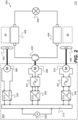
- FIG. 3 is a circuit diagram showing the first power converter 230 and the first electric motor 260 in more detail.
- the DC-DC converter 230 is an isolated DC-DC converter 230 which includes a transformer 259 having an input coil 259' and an output coil 259", with the input side of the DC-DC converter 230 comprising the input coil 259' of the transformer and the output side of the DC-DC converter 230 comprising the output coil 259" of the transformer.
- the input side of the DC-DC converter 230 is galvanically isolated from the output side of the DC-DC converter 230, but the input side of the DC-DC converter 230 is electromagnetically coupled to the output side of the DC-DC converter 230 by the transformer 259.
- the input side of the DC-DC converter 230 is configured to receive the input DC voltage from the DC power supply 220 via the DC bus 210 through input terminals 232, 234.
- the output side of the DC-DC converter is configured to supply the output DC voltage to the first electric motor 260 through a pair of output terminals 236, 238.
- the first electric motor 260 is shown in FIG. 3 as comprising a winding 261, which may include any suitable combination of a resistive load, an inductive load and a capacitive load.
- the winding 261 may be more generally referred to as a load 261.
- the input side of the DC-DC converter 230 comprises a plurality of switches and the input coil 259' of the transformer 259.
- the plurality of input switches are arranged, in this example, as first and second input half-bridges.
- the first input half-bridge comprises a first high-side switch 651 and a first low-side switch 652, while the second input half-bridge comprises a second high-side switch 653 and a second low-side switch 654. Therefore, the input side of the DC-DC converter 230 comprises a plurality of high-side switches 651, 653 and a plurality of low-side switches 652, 654.
- a first terminal of the input coil 259' is coupled to a first input half-bridge output node 612 between the first high-side switch 651 and the first low-side switch 652 of the first input half-bridge.
- a second terminal of the input coil 259' is coupled to a second input half-bridge output node 614 between the second high-side switch 653 and the second low-side switch 654 of the second input half-bridge.
- the output side of the DC-DC converter 230 comprises a plurality of output switches and the output coil 259" of the transformer 259.
- the plurality of output switches are arranged, in this example, as first and second output half-bridges.
- the first output half-bridge comprises a first high-side switch 661 and a first low-side switch 662
- the second output half-bridge comprises a second high-side switch 663 and a second low-side switch 666.
- a first terminal of the output coil 259" is coupled to a first output half-bridge output node 622 between the first high-side switch 661 and the first low-side switch 662 of the first output half-bridge.
- a second terminal of the output coil 259" is coupled to a second output half-bridge output node 624 between the second high-side switch 663 and the second low-side switch 664 of the second output half-bridge.
- the plurality switches of the input side and the input coil 259' of the transformer 259 are mutually connected to each other in a typical dual active bridge power converter arrangement.
- the plurality of output switches of the output side and the output coil 259" of the transformer 259 are mutually connected to each other in a typical dual active bridge converter arrangement.
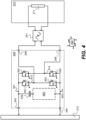
- FIG. 4 is a circuit diagram showing the second power converter 240 and the second electric motor 270 in more detail.
- the second power converter 240 shares some common features with the first power converter 230 described above with reference to FIG. 3 , with those common features being denoted using like reference signs.
- the second power converter 240 is a single-phase AC-DC converter 240 comprising an H-bridge inverter circuit.
- the second power converter 240 therefore does not comprise a transformer or a plurality of output switches.
- the plurality of input switches 651, 652, 653, 654 are arranged as a first half-bridge (comprising a first high-side switch 651 and a first low-side switch 652) and a second half-bridge (comprising a second high-side switch 652 and a second low-side switch 654) which together form a single-phase H-bridge inverter circuit, as will be recognisable to those skilled in the art.
- the input side of the single-phase AC-DC converter 240 is configured to receive the input DC voltage from the DC power supply 220 via the DC bus 210 through input terminals 242, 244.
- the output side of the single-phase AC-DC converter 240 is configured to provide the output AC voltage to the second electric motor 270 through a pair of output terminals 246, 248.
- the second electric motor 270 is shown by FIG. 4 as comprising a winding 271, which may include any suitable combination of a resistive load, an inductive load and a capacitive load.
- a first half-bridge output node 612 is connected to a first terminal of the motor winding 271 and a second half-bridge output node 614 is connected to a second terminal of the motor winding 271 (each through the single-phase filter 241 described above with reference to FIG. 2 ).
- the winding 271 may be more generally referred to as a load 271.
- the third power converter 250 is a three-phase AC-DC converter 250.
- the third power converter 250 therefore comprises first, second and third half-bridges, each comprising a respective high-side switch 651, 653, 655 and a respective low-side switch 652, 654, 656.
- the first, second and third half-bridges are arranged so as to form a three-phase H-bridge inverter circuit, as will be recognisable to those skilled in the art.
- the input side of the three-phase AC-DC converter 250 is configured to receive the input DC voltage from the DC power supply 220 via the DC bus 210 through input terminals 252, 254.
- the output side of the three-phase AC-DC converter 250 is configured to supply the output AC voltages to the third electric motor 280 through first, second and third output terminals 256, 257, 258.
- the third electric motor 280 is shown by FIG. 5 as comprising first, second and third windings 281, 282, 283, each of which may include any suitable combination of a resistive load, an inductive load and a capacitive load.
- the first, second and third windings 281, 282, 283 are arranged in a delta configuration, but this is purely for illustrative purposes.
- first, second and third windings 281, 282, 283 may be arranged in a wye configuration.
- a first half-bridge output node 612 is coupled to and between a terminal of the first motor winding 281 and a terminal of the second motor winding 282, a second half bridge output node 614 is connected to and between a terminal of the second motor winding 282 and a terminal of the third motor winding 283, and a third half bridge output node 616 is connected to and between a terminal of the third motor winding 283 and a terminal of the first motor winding 281 (each through the three-phase filter 251 described above with reference to FIG. 2 ).
- the windings 281, 282, 283 may be more generally and simply referred to as loads 281, 282, 283.
- a first input connection rail 231, 241, 251 extends between the first input terminal 232, 242, 252 and the first high-side switch 651 to provide an electrical connection between the first input terminal 232, 242, 252 and the plurality of high-side switches 651, 653, 655.
- a second input connection rail 233, 243, 253 extends between the second input terminal 234, 244, 254 and the first low-side switch 652 to provide an electrical connection between the second input terminal 234 and the plurality of low-side switches 652, 654, 656.
- the first input connection rail 231, 241, 251 is connected to a positive terminal of the DC power supply 220 via the DC bus 210 whereas the second input connection rail 233, 243, 253 is connected to a reference voltage (e.g. ground or negative) terminal of the DC power supply 220 via the DC bus 210.
- a reference voltage e.g. ground or negative
- an electric potential of the first input connection rail 231, 241, 251 is higher than an electric potential of the second input connection rail 233, 243, 253 during use. Therefore, the first input connection rail 231, 241, 251 may be referred to as a positive input connection rail 231, 241, 251 and the second input connection rail 233, 243, 253 may be referred to as a negative input connection rail 233, 243, 253.
- the first input connection rail 231, 241, 251 and the second input connection rail 233, 243, 253 together form a DC link of the power converter 230, 240, 250.
- a DC link capacitor 630 is couplable between the input terminals 232, 234, 242, 244, 252, 254, in parallel with the (input) half-bridges 651, 652, 653, 654, 655, 656. Accordingly, the capacitor 630 can be coupled so as to receive the voltage supplied by the DC bus 210. The capacitor 630 therefore acts to smooth the voltage received by the (input) half-bridges by reducing temporal variations (i.e., ripple) in the voltage supplied by the DC bus 210.
- the capacitor 630 comprises a first terminal and a second terminal, each of which correspond to a respective side (e.g., a respective plate) of the capacitor 630.
- the first terminal of the capacitor 630 is electrically coupled to the first input connection rail 231, 241, 251 while the second terminal of the capacitor 630 is electrically coupled to a routing unit 680.
- the routing unit 680 is in turn electrically coupled to the second input connection rail 233, 243, 253.
- the routing unit 680 comprises a routing switch, as described in further detail with respect to the example topologies shown in FIGs. 6A-6E below.
- Each power converter 230, 240, 250 is functionally provided with (e.g., comprises) a respective controller 290 configured to control operation of the power converter.
- the controller 290 is communicatively coupled with each of the plurality of input switches, each of the plurality of output switches (if present) as well as the routing unit 680.
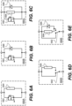
- FIG. 6A is a circuit diagram showing a first example routing unit topology 680A suitable for use as in the routing unit 680 as part of any of the example power converters 230, 240, 250 described above with reference to FIGs. 3-5 .
- the routing unit 680A comprises a switch 682 (which may be referred to herein as a routing switch 682) positioned such that, when the routing unit 680A is incorporated within the power converter 230, 240, 250, the routing switch 682 is connected in series between the second terminal of the capacitor 630 and the second input connection rail. That is, the second terminal of the capacitor 630 is electrically coupled to the second input connection rail via the routing switch 682.
- the routing switch 682 is coupled in series with the capacitor 630 such that a series combination of the capacitor 630 and routing switch 682 is coupled in parallel with respect to both the input terminals 232, 234, 242, 244, 252, 254 and each input half-bridge.
- the routing switch 682 is a field effect transistor (FET).
- FET field effect transistor
- other types of switches useable as part of a routing unit 680 for the purposes described herein will now be apparent to those skilled in the art.
- the routing unit 680A also comprises a resistor 684 (which may be referred to herein as a routing resistor 684) coupled in parallel with the routing switch 682 such that, when the routing unit 680A is incorporated within the power converter 230, 240, 250, the routing resistor 684 is coupled in series between the second terminal of the capacitor 630 and the second input connection rail 233, 243, 253. In this way, the routing resistor 684 is coupled in series with the capacitor 630 such that a series combination of the capacitor 630 and routing resistor 684 is coupled in parallel with respect to both the input terminals 232, 234, 242, 244, 252, 254 and each input half-bridge.
- a resistor 684 (which may be referred to herein as a routing resistor 684) coupled in parallel with the routing switch 682 such that, when the routing unit 680A is incorporated within the power converter 230, 240, 250, the routing resistor 684 is coupled in series between the second terminal of the capacitor 630 and the second input connection rail 233
- the routing unit 680A provides two possible current paths between the second terminal of the capacitor 630 and the second input connection rail 233, 243, 253 of the power converter 230, 240, 250: one through the routing switch 682 (bypassing the routing resistor 684) and another through the routing resistor 684.
- the routing switch 682 When the routing switch 682 is in an open or off state (i.e., a state in which it does not conduct), only the current path through the routing resistor 684 is available.
- the routing switch 682 is in a closed or on state (i.e., a state in which it conducts), both of the current paths discussed above are available.
- the routing switch 682 when the routing switch 682 is in a closed or on state (i.e., a state in which it does conduct), the current path through the routing FET switch 682 has a significantly lower resistance than the current path through the routing resistor 684 and thus current flows through the routing FET switch 682 from the second terminal of the capacitor 630 to the second input connection rail 233 243, 253.
- FIG. 6B is a circuit diagram showing a second example routing unit topology 680B suitable for use in the routing unit 680 as part of any of the example power converters 230, 240, 250 described above with reference to FIGs. 3-5 .
- the routing unit 680B is generally similar to the routing unit 680A described above with reference to FIG. 6A , with like reference signs denoting common features.
- the routing resistor 684 has been replaced with a diode 686 (which may be referred to herein as a routing diode 686).
- the routing diode 686 is coupled in parallel with the routing switch 682 such that, when the routing unit 680B is incorporated within the power converter 230, 240, 250, the routing diode 686 is coupled in series between the second terminal of the capacitor 630 and the second input connection rail 233, 243, 253, with an anode of the routing diode 686 being coupled to the second input connection rail 233, 243, 253 and a cathode of the routing diode 686 being coupled to the second terminal of the capacitor 630.
- routing diode 686 is coupled in series with the capacitor 630 such that a series combination of the capacitor 630 and routing diode 686 is coupled in parallel with respect to both the input terminals 232, 234, 242, 244, 252, 254 and each input half-bridge.
- the routing unit 680B provides two possible current paths between the second input connection rail 233, 243, 253 of the power converter 230, 240, 250 and the second terminal of the capacitor 630: one through the routing switch 682 and another through the routing diode 686.
- the routing switch 682 When the routing switch 682 is in the open state, current cannot flow from the second terminal of the capacitor 630 to the second input connection rail 233, 243, 253 of the power converter 230, 240, 250, because there is no current path through the routing switch 682, and the routing diode 686 is reverse biased, thus blocking current flow from the second terminal of the capacitor 630 to the second input connection rail 233, 243, 253 of the power converter 230, 240, 250.
- FIG. 6C is a circuit diagram showing a third example routing unit topology 680C suitable for use in the routing unit 680 as part of any of the example power converters 230, 240, 250 described above with reference to FIGs. 3-5 .
- the routing unit 680C is generally similar to the routing units 680A, 680B described above with reference to FIGs. 6A and 6B , with like reference signs denoting common features.
- the routing unit 680C comprises both a routing resistor 684 and a routing diode 686.
- the routing resistor 684 and the routing diode 686 are connected in parallel with the routing switch 682 such that, when the routing unit 680C is incorporated within the power converter 230, 240, 250, the routing resistor 684 and routing diode 686 are each coupled in series between the second terminal of the capacitor 630 and the second input connection rail 233, 243, 253, with an anode of the routing diode 686 being coupled to the second input connection rail 233, 243, 253 and a cathode of the routing diode being coupled to the second terminal of the capacitor 630.
- the routing unit 680C provides three possible current paths between the second terminal of the capacitor 630 and the second input connection rail 233, 243, 253 of the power converter 230, 240, 250: one through the routing FET switch 682, another through the routing resistor 684 and yet another through the routing diode 686.
- the routing FET switch 682 When the routing FET switch 682 is in the open state, current can only flow from the second terminal of the capacitor 630 to the second input connection rail 233, 243, 253 of the power converter 230, 240, 250 through the resistor 684, because there is no current path through the routing switch 682, and the routing diode 686 is reverse biased. However, current can flow from the second input connection rail 233, 243, 253 of the power converter 230, 240, 250 to the second terminal of the capacitor 630 through the resistor 684 or the routing diode 686.
- routing switch 682 when the routing switch 682 is in the open state, conventional electric current electric current will generally preferentially flow from the second input connection rail 233, 243, 253 to the second terminal of the capacitor 630 through the current path through the diode 686 rather than through the current pathway through the routing resistor 684 due to a significantly lower impedance associated with the former.
- FIGs. 6D and 6E are circuit diagrams showing a fourth and fifth example routing unit topologies 680D, 680E suitable for use as in the routing unit 680 as part of any of the example power converters 230, 240, 250 described above with reference to FIGs. 3-5 .
- the fourth and fifth example routing unit topologies 680D, 680E are generally similar to the first and third example routing unit topologies 680A, 680C described above with reference to FIGs. 6A and 6C .
- the routing switch 682 is a single-pole double-throw (SPDT) switch (e.g., a SPTD relay) rather than a FET.
- SPDT single-pole double-throw
- the layout of the fifth example routing unit topology 680E differs to that of the third example routing unit topology 680C so as to ensure that the resistor 684 and the diode 686 are always connected in parallel with each other regardless of the position of the SPDT switch 682.
- the routing SPDT switch 682 When the routing SPDT switch 682 is in a first state thereof (i.e., the state shown in FIGs. 6D-6E ), the only current path between the second terminal of the capacitor 630 and the second input connection rail 233, 243, 253 which is available bypasses the resistor 684 and/or the diode 686, as the case may be. In contrast, when the routing SPDT switch 682 is in a second state thereof (i.e., the state not shown in FIGs. 6D-6E ), one or more current pathways between the second terminal of the capacitor 630 and the second input connection rail 233, 243, 253 are available, each of which passes through the resistor 684 or the diode 686, as the case may be.
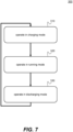
- FIG. 7 is a flowchart showing an example method 300 of operating a power converter (e.g., any of the example power converters described above with respect to FIGs. 3-5 ) in accordance with the present disclosure.
- the method(s) described herein may be carried out by a suitable data processing apparatus, such as the controller 290 described above with respect to FIGs. 3-5 .
- the controller 290 may be configured to carry out the method(s) described herein (e.g., the method 300).
- the method 300 includes an action of operating, at block 310, the power converter in a DC link charging mode (which may be referred to using reference numeral 310) during which a charging process is performed to charge the DC link capacitor 630.
- the action of operating the power converter 230, 240, 250 in the charging mode 310 includes controlling the half-bridges such that current may not flow from the first input connection rail 231, 241, 251 of the power converter 230, 240, 250 to the second input connection rail 233, 243, 253 of the power converter 230, 240, 250 via the half-bridges and/or via the load(s) 261, 271, 281, 282, 283.
- the action of operating the power converter 230, 240, 250 in the charging mode 310 includes opening one or both of the high-side switch and the low-side switch of each of the half-bridges such that current cannot flow through any of the half-bridges from the first input connection rail 231, 241, 251 of the power converter 230, 240, 250 to the second input connection rail 233, 243, 253 of the power converter 230, 240, 250 s.
- the action of operating the power converter 230, 240 in the charging mode 310 includes opening both the first high-side switch 651 and the second high-side switch 651 (and maintaining these switches in an open or off state in which they do not conduct) and/or opening both the first low-side switch 652 and the second low-side switch 654 (and maintaining these switches in the open state).
- the action of operating the power converter 250 in the charging mode 310 includes maintaining each of the first high-side switch 651, the second high-side switch 653 as well as the third high-side switch 653 and/or each of the first low-side switch 652, the second low-side 654 as well as the third low-side switch 656 in the open state.
- the action of operating the power converter 230, 240, 250 in the charging mode 310 also includes forming a charge circuit for charging the capacitor 630 using the input DC voltage received from the DC bus 210.
- the action of operating the power converter 230, 240, 250 in the charging mode 310 may include controlling the routing unit 680 appropriately such that the resistor 684 (if present) and/or the diode 684 (if present) forms a part of the charge circuit.
- appropriate control of the routing unit 680 in the charging mode 310 may include controlling the routing switch 682 such that the only conduction path between the second terminal of the capacitor 630 and the second input connection rail 233, 243, 253 includes the resistor 684.
- appropriate control of the routing unit 680 may include maintaining the routing switch 682 in the open state thereof (i.e., in the non-conducting state).
- appropriate control of the routing unit 680 may include maintaining the routing SPDT switch 682 in the second state thereof (i.e., the state not shown in FIGs. 6D-6E ).
- Inclusion of the resistor 684 within the charge circuit formed in the charging mode 310 ensures that a peak electric current flowing through the charge circuit is effectively limited by the impedance of the resistor 684. That is, a transient inrush current associated with electrical coupling of the terminals of the capacitor 630 to the DC bus 210 may be limited by control of the routing unit 680 in the manner described above.
- the power converter 230, 240, 250 may be operated in the charging mode 310 until a potential difference across the capacitor 630 (i.e., a voltage of the DC link) has reached (e.g., is equal to or greater than) a predetermined precharging voltage threshold.
- the precharging voltage threshold may be set having regard to the operating voltage of the DC bus 210.
- the precharging voltage threshold may be set as being equal to, or within a tolerance range of, the operating voltage of the DC bus 210. This facilitates a smooth transition from operation of the power converter 230, 240, 250 from the charging mode 310 another mode, such as the running mode discussed below with reference to block 320.
- the potential difference across the capacitor 630 reaches the precharging voltage threshold, the charging process undergone in the charging mode 310 may be described as being complete.
- a rate at which the capacitor 630 charges to the precharging voltage threshold is dependent, at least in part, by a total impedance of the charge circuit.
- a relatively lower total impedance of the charge circuit will result in faster charging of the capacitor 630 than a relatively higher total impedance of the charge circuit.
- the method 300 also includes an action of operating, at block 320, the power converter in a running mode (which may be referred to using reference numeral 320).
- the action of operating the power converter in the running mode 320 includes controlling of each of the half-bridges to convert the input DC voltage into the relevant output voltage(s) (e.g., the output DC voltage, the output AC voltage, or the output AC voltages as applicable).
- One or more operating parameters of the input switches e.g. a switching frequency, a switching phase or a duty cycle of each of the plurality of input switches may be controlled to convert the input DC voltage into the relevant output voltage(s).
- the operating parameter of each of the plurality of input switches may be controlled in the running mode 320 to vary the conversion ratio of the DC-DC converter 230 between a small non-zero value which is less than unity, and a large non-infinite value which is greater than unity.
- a corresponding parameter of each of the plurality of output switches e.g., a duty cycle and/or a switching frequency
- the output DC voltage for provision to the first motor 260 via the pair of output terminals 236, 238 may be controlled (e.g., varied) in this manner.
- Operating the first power converter 230 in the running mode 320 may thus allow the first power converter 230 to be used as a DC motor drive for the first motor 260.
- the operating parameter of each of the plurality of input switches may be controlled in the running mode 320 to vary the frequency of the output AC voltage for supply to the second electric motor 270 via the output terminals 246, 248.
- the output AC voltage provided to the second motor 270 via the pair of output terminals 246, 248 may be controlled (e.g., varied) in this way.
- Operating the second power converter 240 in the running mode 320 may thus allow the second power converter 240 to be used as an AC motor drive (e.g., a variable frequency AC motor drive) for the second motor 270.
- the or each operating parameter of each of the plurality of input switches may be controlled in the running mode 320 to vary the frequency and/or the phase of the output AC voltages for supply to the third electric motor 280 via the output terminals 256, 258.
- the output AC voltages provided to the third motor 280 via the output terminals 256, 257, 258 may be controlled (e.g., varied) in this manner.
- Operating the third power converter 250 in the running mode 320 may thus allow the third power converter 270 to be used as a three-phase AC motor drive (e.g., a variable frequency and/or variable phase AC motor drive) for the third motor 280.
- the action of operating the power converter 230, 240, 250 in the running mode 320 may also include controlling the routing unit 680 to provide a current path between the capacitor 630 and the second input connection rail 233, 243, 253/the input switches which bypasses the resistor 684 (see FIGs. 6A-6E ).
- control of the routing unit 680 in the running mode 320 may include controlling the routing switch 682 such that a conduction path between the second terminal of the capacitor 630 and the second input connection rail 233, 243, 253 which does not include the resistor 684 is available.
- the routing unit topologies 680A-680C described above with reference to FIGs.
- control of the routing unit 680 may include closing the routing switch 682 (and maintaining it in the closed state).
- control of the routing unit 680 may include maintaining the routing SPDT switch 682 in the first state thereof (i.e., the state shown in FIGs. 6D-6E ).
- Provision of current path between the capacitor 630 and the second input connection rail 233, 243, 253 which bypasses the resistor 684 in the running mode 320 reduces energy losses (e.g., Ohmic losses) within the routing unit 680 as the capacitor 630 acts to smooth the voltage received from the DC bus 210.
- energy losses e.g., Ohmic losses
- control of the or each operating parameter of each of the input switches is effected so as to ensure that a short-circuit across any of the input half-bridges es with respect to the DC bus 210 (i.e., a shoot-through condition) is not possible.
- a high-side switch 651, 653, 655 and a low-side switch 652, 654, 656 belonging to the same input half-bridge should never be simultaneously in a closed or on state (i.e., a state in which they do conduct).
- Such a control regime may be referred to as providing shoot-through protection for the power converter 230, 240, 250.
- the method 300 further includes an action of operating, at block 330, the power converter in a discharging mode (which may be referred to using reference numeral 330) during which a discharging process is undergone.
- the action of operating the power converter 230, 240, 250 in the discharging mode 330 includes controlling the plurality of input switches to establish a current path between the first terminal of the capacitor 630 and the second terminal of the capacitor 630.
- the action of operating the power converter 230, 240, 250 in the discharging mode 330 includes closing at least one of the high-side switches and at least one of the low-side switches, to create a current path from the first terminal of the capacitor 630 via the first input connection rail 231, 241, 251, the closed high-side switch(es) 651, 653, 655, the closed low-side switch(es) 652, 654, 656, the second input connection rail 233, 243, 253 and the routing unit 680 to the second terminal of the capacitor 630.
- the action of operating the power converter 230, 240 in the discharging mode 330 includes maintaining both the first high-side switch 651 and the first low-side 652 and/or both the second high-side switch 653 and the second low-side switch 654 in the closed state.
- the action of operating the power converter 250 in the charging mode 310 includes maintaining both the first high-side switch 651 and the first low-side switch 652 in the closed state, both the second high-side switch 653 and the second low-side 654 in the closed state and/or both the third high-side switch 655 and the third low-side switch 656 in the closed state.
- operation of the power converter 230, 240, 250 in the discharging mode comprises simultaneously maintaining a high-side switch 651, 653, 655 and a low-side switch 652, 654, 656 belonging to the same input half-bridge in the closed state.
- operation of the power converter 230, 240, 250 in the discharging mode 330 in the manner described above involves the adoption of control action(s) which contravene(s) the principles for preventing a shoot-through condition discussed above with respect to the running mode 620. That is, in order to operate the power converter 230, 240, 250 in the discharging mode 330, it may be necessary to override and/or disable the shoot-through protection which the data processing apparatus carrying out the method 300 may otherwise be configured to provide.
- the action of operating the power converter 230, 240, 250 in the discharging mode 330 further includes forming a discharge circuit for discharging the capacitor 630 through the routing unit 680.
- the action of operating the power converter 230, 240, 250 in the discharge mode 330 may include controlling the routing unit 680 appropriately such that the resistor 684 and/or the diode 686 forms a part of the discharge circuit.
- Appropriate control of the routing unit 680 in the discharge mode 330 may include controlling the routing switch 682 such that the only current path between the second terminal of the capacitor 630 and the second input connection rail 233, 243, 253 includes the resistor 684 and/or the diode 686.
- appropriate control of the routing unit 680 may include maintaining the routing switch 682 in the open state .
- appropriate control of the routing unit 680 may include maintaining the routing SPDT switch 682 in the second state thereof (i.e., the state not shown in FIGs. 6D-6E ).
- the power converter 230, 240, 250 may be operated in the discharging mode 330 until a potential difference across the capacitor 630 has fallen to (e.g., is equal to or less than) a predetermined discharging voltage threshold.
- the discharging voltage threshold may be set having regard to a safe condition of the capacitor 630.
- the discharge voltage threshold may be set as being equal to, or within a tolerance range of, a value of the potential difference across the capacitor 630 which is considered not to pose a risk to the safety of operators who may come into electrical contact with the electrical system 200 and/or the power converter 230, 240, 350.
- the discharge voltage threshold may be substantially or exactly zero.
- a rate at which the capacitor 630 discharges to the discharge voltage threshold is dependent, at least in part, on a total impedance of the discharge circuit.
- a relatively lower total impedance of the charge circuit will result in faster discharging of the capacitor 630 than a relatively higher total impedance of the discharge circuit.
- the topology of the routing unit 680 may generally be selected according to a preference for a length of the time taken to complete the charging process (in the charging mode 310) and/or the discharging process (in the discharging mode 330). If a relatively fast charging/discharging process (i.e., a shorter length of time taken to complete the charging/discharging process) is preferred, the routing unit topologies 680B, 680C, 680E including the diode 686 may be selected for use because the diode 686 may typically have a lower impedance than the resistor 684.
- routing unit topologies 680A, 680C, 680D including the resistor 684 may be selected for use. If different speeds to complete the charging and discharging processes, respectively, are preferred, routing unit topologies 680C, 680E comprising both the resistor 684 and the diode 686 coupled in parallel with respect to each other may be selected for use.
- either of the routing unit topologies 680C, 680E shown by FIGs. 6C and 6E may be selected for use. Because of the orientation of the diode 686, when the routing switch 682 is controlled in the charging mode 310 as described above, conventional current may not flow from the second terminal of the capacitor 630 to the second input connection rail 233, 243, 253 through the diode 686. Therefore, conventional current must flow through the resistor 684 in order to charge the capacitor 630 in the charging mode 310.
- the effective impedance of the charge circuit is relatively high and the time taken to complete the charging process is relatively long.
- conventional current may flow from the second input connection rail 233, 243, 253 to the second terminal of the capacitor 630 through the diode 686.
- conventional current can flow through the either the resistor 684 or the diode 686 in order to discharge the capacitor 630 in the discharging mode 330. Accordingly, the effective impedance of the discharge circuit is relatively low and the time taken to complete the discharging process is relatively short.
- routing unit topologies which are similar to those shown by FIGs. 6C and 6E , but in which the orientation of the diode 686 has been reversed compared to the orientation shown by FIGs. 6C and 6E , may instead be selected for use.
- the charge circuit and the discharge circuit formed in the examples described herein is disposed entirely within the power converter 230, 240, 250, which is associated with an increased safety of the power converter 230, 240, 250.
- the charge circuit and the discharge circuit formed in the examples described herein includes only passive components, which provides a less complex and/or more robust power converter 230, 240, 250.
- methods in accordance with the present disclosure may comprise only one, or any combination, of the charging mode, the running mode and the discharging mode. Further, it will be appreciated that a power converter may only be operated in one of these modes at any one time, and so methods in accordance with the present disclosure which comprise more than one of the charging mode, the running mode and the discharging mode include selectively (e.g., alternately) operating a power converter in the charging mode, the running mode or the discharging mode, as the case may be.
- FIG. 8 shows, highly schematically, a machine-readable medium 600 having stored thereon a computer program 60 comprising instructions which, when executed by the controller 290 provided to a power converter in accordance with the present disclosure (e.g., any of the power converters described with reference to FIGs. 3-5 ), cause the controller 290 to execute the method 300 described above with reference to FIG. 7 .
- a power converter in accordance with the present disclosure
Landscapes
- Engineering & Computer Science (AREA)
- Power Engineering (AREA)
- Dc-Dc Converters (AREA)
Abstract
The present disclosure relates to a method 300 of controlling a power converter 230, 240, 250. The power converter 230, 240, 250 comprises: input terminals 232, 234, 242, 244, 252, 254 configured to receive an input voltage; a plurality of input switches 651-656 configured as one or more half-bridges, each half bridge comprising a high-side input switch 651, 653, 655 and a low-side input switch 652, 654, 656; and a capacitor 630 couplable to the input terminals 232, 234, 242, 244, 252, 254 so as to receive the input voltage. The method 300 comprises: operating the power converter 230, 240, 250 in a discharging mode 330 which comprises closing a high-side input switch 651, 653, 655 and a low-side input switch 652, 654, 656 to complete a discharge circuit between first and second terminals of the capacitor 630. The present disclosure further relates to a power converter 230, 240, 250 comprising means 290 adapted to carry out such a method 300.
Description
- The present disclosure relates to methods of controlling a power converter. The present disclosure also relates to power converters comprising means adapted to carry out such methods.
- It is known to provide means for precharging and/or discharging a DC link of a power converter. Such means may include dedicated precharging and/or discharging circuitry coupled to the power converter and controllable to supply electrical energy to, or receive electrical energy from, the power converter for these purposes. Precharging the DC link of a power converter is associated with improved operation of the power converter during use, whereas discharging the DC link of a power converter is associated with better safety of the power converter after use.
- Conventional methods and means of precharging and/or discharging the DC link of a power converter may require the use of large active charge/discharge circuits. Additionally or alternatively, conventional methods and means for precharging and/or discharging the DC link of a power converter may affect the operation of other components of an electrical system of which the power converter forms a part. For example, if a power converter is electrically coupled to an electrical bus which is configured to act as an intermediary between the power converter and other electrical components (e.g., other power converters) of an electrical system, precharging and/or discharging of the DC link of the power converter using conventional techniques may require the decoupling of the other electrical components from the electrical bus and/or variation of the operation of the other electrical components.
- It is desirable to provide improved methods and means of precharging and/or discharging the DC link of a power converter. It is particularly desirable to provide improved methods and means of discharging a power converter. The present invention has been devised with the foregoing in mind.
- According to a first aspect there is provided a method of controlling a power converter, the power converter comprising: input terminals configured to receive an input voltage; a plurality of input switches configured as one or more half-bridges, each half bridge comprising a high-side input switch and a low-side input switch; and a capacitor couplable to the input terminals so as to receive the input voltage, the method comprising: operating the power converter in a discharging mode which comprises closing a high-side input switch and a low-side input switch to complete a discharge circuit between first and second terminals of the capacitor.
- It may be that the method comprises selectively operating the power converter in the discharging mode or a running mode, wherein operating the power converter in the running mode comprises controlling the plurality of input switches to generate an output voltage based on the input voltage.
- It may also be that the method comprises selectively operating the power converter in the discharging mode, the running mode or a charging mode, wherein operating the power converter in the charging mode comprises maintaining each high-side switch and/or each low-side switch in an open state and wherein, in the charging mode, the capacitor is electrically coupled to the pair of input terminals.
- It may be that the power converter further comprises a resistor couplable in series with the capacitor such that a series combination of the capacitor and resistor is coupled in parallel with the input terminals and the or each half-bridge.
- It may be that, in the charging mode, the capacitor is electrically couplable to the input terminals via the resistor.
- It may be that the power converter further comprises a routing switch couplable in series with the capacitor such that a series combination of the capacitor and routing switch is coupled in parallel with the input terminals and the or each half-bridge. Operating the power converter in the running mode may include controlling the routing switch to provide a current path between the capacitor and one of the plurality of input switches which bypasses the resistor. The resistor may form a part of the discharge circuit.
- It may be that the power converter further comprises a diode couplable in series with the capacitor such that a series combination of the capacitor and diode is coupled in parallel with the input terminals and the or each half-bridge.
- It may be that the power converter further comprises a routing switch couplable in series with the capacitor such that a series combination of the capacitor and routing switch is coupled in parallel with the input terminals and the or each half-bridge. Operating the power converter in the running mode includes controlling the routing switch to provide a current path between the capacitor and one of the input switches which bypasses the diode. The diode may form a part of the discharge circuit.
- It may be that the resistor and the diode are coupled in parallel with each other.
- It may be that operating the power converter in the discharging mode comprises closing a high-side switch and a low-side switch of the same half-bridge.
- The discharge circuit completed in the discharging mode may be entirely disposed within the power converter.
- It may be that the power converter is configured to supply an output voltage to a winding of a motor, and wherein the winding forms a part of the discharge circuit.
- According to a second aspect there is provided a power converter comprising input terminals, a plurality of input switches, a capacitor and means adapted to carry out a method in accordance with the first aspect.
- According to a third aspect there is provided a computer program comprising instructions to cause a power converter in accordance with the second aspect to execute the steps of a method in accordance with the first aspect.
- According to a fourth aspect there is provided a computer-readable medium having stored thereon a computer program in accordance with the third aspect.
- According to a fifth aspect there is provided an electrical system comprising a multiplicity of power converters, each power converter being in accordance with a power converter in accordance with the second aspect.
- According to a sixth aspect there is provided a transport refrigeration unit comprising a power converter in accordance with the second aspect or an electrical system in accordance with the fifth aspect.
-
-
FIG. 1 shows a vehicle comprising a transport refrigeration system; -
FIG. 2 is a schematic diagram of example transport refrigeration unit suitable for use with the vehicle ofFIG. 1 , the example transport refrigeration unit comprising an electrical system and a vapour-compression refrigeration circuit; -
FIG. 3 is a circuit diagram which shows a first example power converter suitable for use with the electrical system ofFIG. 2 ; -
FIG. 4 is a circuit diagram which shows a second example power converter suitable for use with the electrical system ofFIG. 2 ; -
FIG. 5 is a circuit diagram which shows a third example power converter suitable for use with the electrical system ofFIG. 2 ; -
FIGs. 6A-6E are circuit diagrams which show example routing units suitable for use with any of the example power converters ofFIGs. 3-5 ; -
FIG. 7 is a flowchart which shows an example method of operating a power converter in accordance with the present disclosure; and -
FIG. 8 is a highly schematic diagram of a machine-readable medium having stored thereon a computer program which, when executed by a controller, causes the controller to perform the example method ofFIG. 7 . -
FIG. 1 shows avehicle 10 comprising atransport refrigeration system 20. In the example ofFIG. 1 , thetransport refrigeration system 20 forms a part of an over-the-road refrigerated semi-trailer having astructure 22 supporting (or forming) at least one climate-controlledcompartment 24 which is configured to be cooled and/or heated by a TRU 110. The climate-controlledcompartment 24 can take the form of multiple compartments or have multiple zones. Thestructure 22 includes a chassis. Thestructure 22 supports the TRU 110. Thevehicle 10 further comprises atractor unit 14 removably couplable to the trailer. -
FIG. 2 schematically shows a diagram of an example TRU 110 suitable for use within thevehicle 10 and thetransport refrigeration system 20 ofFIG. 1 . The TRU 110 comprises a vapour-compression refrigeration circuit 400 and anelectrical system 200. - The vapour-
compression refrigeration circuit 400 includes anevaporator 408 which is configured to receive heat from the climate-controlledcompartment 24 of thetransport refrigeration system 20 and acondenser 404 which is configured to reject heat to a thermal sink 44 (e.g., ambient air outside of the climate-controlled compartment 24). For these purposes, the vapour-compression refrigeration circuit 400 also includes acompressor 402 and anexpansion valve 406. Accordingly, the vapour-compression refrigeration circuit 400 may be controlled to cause heat to be removed from the climate-controlledcompartment 24. The TRU 110 also comprises a plurality offans FIG. 2 , afirst fan 462 is associated with (e.g., located in proximity to) theevaporator 408 for improving heat transfer at one or more surfaces of theevaporator 408, and asecond fan 464 is associated with (e.g., located in proximity to) thecondenser 404 for improving heat transfer at one or more surfaces of thecondenser 404. - The
electrical system 200 comprises aDC bus 210, aDC power supply 220, a plurality ofpower converters electric motors DC power supply 210 may not form part of theelectrical system 200 as such, and that theDC bus 210 may instead be couplable to, and hence configured to receive electrical power from, aDC power supply 220. - A first electric motor 260 (i.e., a first of the plurality of electric motors) is mechanically coupled to, and is thus configured to mechanically drive, the
first fan 462. A second electric motor 270 (i.e., a second of the plurality of electric motors) is mechanically coupled to, and is configured to mechanically drive, thesecond fan 464. A third electric motor 280 (i.e., a third of the plurality of electric motors) is mechanically coupled to, and is therefore configured to mechanically drive, thecompressor 402. - Thus, the
electrical system 200 may be operated to drive thecompressor 402 and thereby control the vapour-compression refrigeration circuit 400. Thecompressor 402 may be any suitable type of compressor, as will be apparent to those skilled in the art. However, in particular examples, thecompressor 402 may be a reciprocating compressor (e.g., a piston compressor) or a scroll compressor. - A first power converter 230 (i.e., a first of the plurality of power converters) is electrically coupled to, and is configured to electrically drive, the first
electric motor 260. A second power converter 240 (i.e., a second of the plurality of power converters) is electrically coupled to, and is therefore configured to electrically drive, the secondelectric motor 270. A third power converter 250 (i.e., a third of the plurality of power converters) is electrically coupled to, and is therefore configured to electrically drive, the thirdelectric motor 280. - An input side of each
power converter power converter electric motor - The first
electric motor 260 is a DC electric motor and thefirst power converter 230 is a DC-DC converter 230 (e.g., a DC-DC converter 230). The firstelectric motor 260 may be a permanent-magnet DC motor, a series DC motor, a shunt DC motor, a compound DC motor or the like. - The DC-
DC converter 230 is generally configured to convert the input DC voltage supplied to the input side of the DC-DC converter 230 at a first magnitude (i.e., at a magnitude corresponding to the operating voltage of the DC bus 210) to an output DC voltage at a second magnitude for supply to the firstelectric motor 260 from the output side of the DC-DC converter 230. A ratio between the first magnitude and the second magnitude may be referred to as a conversion ratio of the DC-DC converter 230. The conversion ratio of the DC-DC converter 230 is controllable as described in further detail herein. If the conversion ratio of the DC-DC converter 230 is greater than unity, the DC-DC converter 230 performs a boost (or a step-up) function in use. On the other hand, if the conversion ratio of the DC-DC converter is less than unity, the DC-DC converter 230 performs a buck (or a step-down) function in use. - The second
electric motor 270 is a single-phase AC electric motor and thesecond power converter 240 is a single-phase DC-AC power converter 240 (e.g., a single-phase DC-AC converter 240 or a single phase inverter 240). The secondelectric motor 270 may be, for example, an induction motor (i.e., an asynchronous motor). To this end, the secondelectric motor 270 include a main winding, an auxiliary winding, a start capacitor and/or a run capacitor, as will be appreciated by those skilled in the art. - The single-
phase inverter 240 is generally configured to convert the input DC voltage supplied to the input side of the single-phase inverter 240 to an output AC voltage for supply to the secondelectric motor 270 from the output side of the single-phase inverter 240. A frequency of the output AC voltage for supply to the secondelectric motor 270 is controllable as described in further detail herein. - A single-phase
passive filter 241 is electrically coupled between the output side of the single-phase inverter 240 and the secondelectric motor 270. The single-phasepassive filter 241 is configured to attenuate high-frequency components in the output AC voltage supplied to the secondelectric motor 270 from the output side of the single-phase inverter 240 to increase a conformity of a temporal profile of the output AC voltage supplied to the secondelectric motor 270 with a sinusoid. The single-phasepassive filter 241 therefore functions as a low-pass filter in use. The single-phasepassive filter 241 may include a T-filter topology or a pi-filter topology, as will be understood by those skilled in the art. - The third
electric motor 280 is a multiple-phase AC electric motor and thethird power converter 250 is a multiple-phase DC-AC power converter 250 (e.g., a multiple-phase DC-AC converter 250 or a multiple-phase inverter 250). The thirdelectric motor 280 may be, for example, an induction motor (i.e., an asynchronous motor). Consequently, the thirdelectric motor 280 may include a plurality of phase windings, as will be appreciated by those skilled in the art. In this example, the thirdelectric motor 280 is a three-phase AC electric motor. - The multiple-
phase inverter 250 is generally configured to convert the input DC voltage supplied to the input side of the multiple-phase inverter 250 to a plurality of output AC voltages for supply to the thirdelectric motor 280 from the output side of the multiple-phase inverter 250. A frequency and a phase of each output AC voltage for supply to the thirdelectric motor 280 is controllable as described in further detail herein. - A multiple-phase
passive filter 251 is electrically coupled between the output side of the multiple-phase inverter 250 and the thirdelectric motor 280. The multiple-phasepassive filter 251 is configured to attenuate high-frequency components in each of the output AC voltages supplied to the thirdelectric motor 280 from the output side of the multiple-phase inverter 250 to increase a conformity of a temporal profile of each output AC voltage supplied to the thirdelectric motor 280 with a sinusoid. The multiple-phasepassive filter 251 therefore functions as a low-pass filter in use. The multiple-phasepassive filter 251 may include one or more T-filter topologies and/or one or more pi-filter topologies, as will be understood by those skilled in the art. -
FIG. 3 is a circuit diagram showing thefirst power converter 230 and the firstelectric motor 260 in more detail. The DC-DC converter 230 is an isolated DC-DC converter 230 which includes atransformer 259 having an input coil 259' and anoutput coil 259", with the input side of the DC-DC converter 230 comprising the input coil 259' of the transformer and the output side of the DC-DC converter 230 comprising theoutput coil 259" of the transformer. In this way, the input side of the DC-DC converter 230 is galvanically isolated from the output side of the DC-DC converter 230, but the input side of the DC-DC converter 230 is electromagnetically coupled to the output side of the DC-DC converter 230 by thetransformer 259. - The input side of the DC-
DC converter 230 is configured to receive the input DC voltage from theDC power supply 220 via theDC bus 210 throughinput terminals electric motor 260 through a pair ofoutput terminals electric motor 260 is shown inFIG. 3 as comprising a winding 261, which may include any suitable combination of a resistive load, an inductive load and a capacitive load. The winding 261 may be more generally referred to as aload 261. - The input side of the DC-
DC converter 230 comprises a plurality of switches and the input coil 259' of thetransformer 259. The plurality of input switches are arranged, in this example, as first and second input half-bridges. The first input half-bridge comprises a first high-side switch 651 and a first low-side switch 652, while the second input half-bridge comprises a second high-side switch 653 and a second low-side switch 654. Therefore, the input side of the DC-DC converter 230 comprises a plurality of high-side switches 651, 653 and a plurality of low-side switches bridge output node 612 between the first high-side switch 651 and the first low-side switch 652 of the first input half-bridge. A second terminal of the input coil 259' is coupled to a second input half-bridge output node 614 between the second high-side switch 653 and the second low-side switch 654 of the second input half-bridge. - The output side of the DC-
DC converter 230 comprises a plurality of output switches and theoutput coil 259" of thetransformer 259. The plurality of output switches are arranged, in this example, as first and second output half-bridges. The first output half-bridge comprises a first high-side switch 661 and a first low-side switch 662, while the second output half-bridge comprises a second high-side switch 663 and a second low-side switch 666. A first terminal of theoutput coil 259" is coupled to a first output half-bridge output node 622 between the first high-side switch 661 and the first low-side switch 662 of the first output half-bridge. A second terminal of theoutput coil 259" is coupled to a second output half-bridge output node 624 between the second high-side switch 663 and the second low-side switch 664 of the second output half-bridge. - As will be recognisable to those skilled in the art, the plurality switches of the input side and the input coil 259' of the
transformer 259 are mutually connected to each other in a typical dual active bridge power converter arrangement. - As will also be recognisable to those skilled in the art, the plurality of output switches of the output side and the
output coil 259" of thetransformer 259 are mutually connected to each other in a typical dual active bridge converter arrangement. -
FIG. 4 is a circuit diagram showing thesecond power converter 240 and the secondelectric motor 270 in more detail. Thesecond power converter 240 shares some common features with thefirst power converter 230 described above with reference toFIG. 3 , with those common features being denoted using like reference signs. - However, in contrast to the
first power converter 230, thesecond power converter 240 is a single-phase AC-DC converter 240 comprising an H-bridge inverter circuit. Thesecond power converter 240 therefore does not comprise a transformer or a plurality of output switches. The plurality of input switches 651, 652, 653, 654 are arranged as a first half-bridge (comprising a first high-side switch 651 and a first low-side switch 652) and a second half-bridge (comprising a second high-side switch 652 and a second low-side switch 654) which together form a single-phase H-bridge inverter circuit, as will be recognisable to those skilled in the art. - The input side of the single-phase AC-
DC converter 240 is configured to receive the input DC voltage from theDC power supply 220 via theDC bus 210 throughinput terminals DC converter 240 is configured to provide the output AC voltage to the secondelectric motor 270 through a pair ofoutput terminals electric motor 270 is shown byFIG. 4 as comprising a winding 271, which may include any suitable combination of a resistive load, an inductive load and a capacitive load. A first half-bridge output node 612 is connected to a first terminal of the motor winding 271 and a second half-bridge output node 614 is connected to a second terminal of the motor winding 271 (each through the single-phase filter 241 described above with reference toFIG. 2 ). The winding 271 may be more generally referred to as aload 271. -
FIG. 5 is a circuit diagram showing thethird power converter 250 and the thirdelectric motor 280 in more detail. Thethird power converter 250 shares many common features with thesecond power converter 240 described above with reference toFIG. 4 , with those common features being denoted using like reference signs. - In contrast to the
second power converter 240, thethird power converter 250 is a three-phase AC-DC converter 250. Thethird power converter 250 therefore comprises first, second and third half-bridges, each comprising a respective high-side switch side switch - The input side of the three-phase AC-
DC converter 250 is configured to receive the input DC voltage from theDC power supply 220 via theDC bus 210 throughinput terminals DC converter 250 is configured to supply the output AC voltages to the thirdelectric motor 280 through first, second andthird output terminals electric motor 280 is shown byFIG. 5 as comprising first, second andthird windings FIG. 5 , the first, second andthird windings third windings bridge output node 612 is coupled to and between a terminal of the first motor winding 281 and a terminal of the second motor winding 282, a second halfbridge output node 614 is connected to and between a terminal of the second motor winding 282 and a terminal of the third motor winding 283, and a third halfbridge output node 616 is connected to and between a terminal of the third motor winding 283 and a terminal of the first motor winding 281 (each through the three-phase filter 251 described above with reference toFIG. 2 ). Thewindings loads - In each of the examples of
FIGs. 3-5 , a firstinput connection rail first input terminal first input terminal side switches input connection rail second input terminal side switch 652 to provide an electrical connection between thesecond input terminal 234 and the plurality of low-side switches input connection rail DC power supply 220 via theDC bus 210 whereas the secondinput connection rail DC power supply 220 via theDC bus 210. As a result, an electric potential of the firstinput connection rail input connection rail input connection rail input connection rail input connection rail input connection rail input connection rail input connection rail power converter - Further, in each of the examples of
FIGs. 3-5 , aDC link capacitor 630 is couplable between theinput terminals bridges capacitor 630 can be coupled so as to receive the voltage supplied by theDC bus 210. Thecapacitor 630 therefore acts to smooth the voltage received by the (input) half-bridges by reducing temporal variations (i.e., ripple) in the voltage supplied by theDC bus 210. Thecapacitor 630 comprises a first terminal and a second terminal, each of which correspond to a respective side (e.g., a respective plate) of thecapacitor 630. - The first terminal of the
capacitor 630 is electrically coupled to the firstinput connection rail capacitor 630 is electrically coupled to arouting unit 680. Therouting unit 680 is in turn electrically coupled to the secondinput connection rail routing unit 680 comprises a routing switch, as described in further detail with respect to the example topologies shown inFIGs. 6A-6E below. - Each
power converter respective controller 290 configured to control operation of the power converter. To this end, thecontroller 290 is communicatively coupled with each of the plurality of input switches, each of the plurality of output switches (if present) as well as therouting unit 680. -
FIG. 6A is a circuit diagram showing a first examplerouting unit topology 680A suitable for use as in therouting unit 680 as part of any of theexample power converters FIGs. 3-5 . Therouting unit 680A comprises a switch 682 (which may be referred to herein as a routing switch 682) positioned such that, when therouting unit 680A is incorporated within thepower converter routing switch 682 is connected in series between the second terminal of thecapacitor 630 and the second input connection rail. That is, the second terminal of thecapacitor 630 is electrically coupled to the second input connection rail via therouting switch 682. Therefore, therouting switch 682 is coupled in series with thecapacitor 630 such that a series combination of thecapacitor 630 androuting switch 682 is coupled in parallel with respect to both theinput terminals routing switch 682 is a field effect transistor (FET). However, other types of switches useable as part of arouting unit 680 for the purposes described herein will now be apparent to those skilled in the art. - The
routing unit 680A also comprises a resistor 684 (which may be referred to herein as a routing resistor 684) coupled in parallel with therouting switch 682 such that, when therouting unit 680A is incorporated within thepower converter routing resistor 684 is coupled in series between the second terminal of thecapacitor 630 and the secondinput connection rail routing resistor 684 is coupled in series with thecapacitor 630 such that a series combination of thecapacitor 630 androuting resistor 684 is coupled in parallel with respect to both theinput terminals - Accordingly, the
routing unit 680A provides two possible current paths between the second terminal of thecapacitor 630 and the secondinput connection rail power converter routing resistor 684. When therouting switch 682 is in an open or off state (i.e., a state in which it does not conduct), only the current path through therouting resistor 684 is available. When therouting switch 682 is in a closed or on state (i.e., a state in which it conducts), both of the current paths discussed above are available. - However, when the
routing switch 682 is in a closed or on state (i.e., a state in which it does conduct), the current path through therouting FET switch 682 has a significantly lower resistance than the current path through therouting resistor 684 and thus current flows through therouting FET switch 682 from the second terminal of thecapacitor 630 to the secondinput connection rail 233 243, 253. -
FIG. 6B is a circuit diagram showing a second examplerouting unit topology 680B suitable for use in therouting unit 680 as part of any of theexample power converters FIGs. 3-5 . Therouting unit 680B is generally similar to therouting unit 680A described above with reference toFIG. 6A , with like reference signs denoting common features. However, in the example shown inFIG. 6B , therouting resistor 684 has been replaced with a diode 686 (which may be referred to herein as a routing diode 686). - The
routing diode 686 is coupled in parallel with therouting switch 682 such that, when therouting unit 680B is incorporated within thepower converter routing diode 686 is coupled in series between the second terminal of thecapacitor 630 and the secondinput connection rail routing diode 686 being coupled to the secondinput connection rail routing diode 686 being coupled to the second terminal of thecapacitor 630. In other words, therouting diode 686 is coupled in series with thecapacitor 630 such that a series combination of thecapacitor 630 androuting diode 686 is coupled in parallel with respect to both theinput terminals - Consequently, the
routing unit 680B provides two possible current paths between the secondinput connection rail power converter routing switch 682 and another through therouting diode 686. When therouting switch 682 is in the open state, current cannot flow from the second terminal of thecapacitor 630 to the secondinput connection rail power converter routing switch 682, and therouting diode 686 is reverse biased, thus blocking current flow from the second terminal of thecapacitor 630 to the secondinput connection rail power converter input connection rail power converter capacitor 630 through therouting diode 686. When therouting switch 682 is in the closed state, current can flow from the second terminal of thecapacitor 630 through therouting switch 682 to the secondinput connection rail power converter input connection rail power converter routing switch 682 and/or therouting diode 686 to the second terminal of thecapacitor 630. -
FIG. 6C is a circuit diagram showing a third examplerouting unit topology 680C suitable for use in therouting unit 680 as part of any of theexample power converters FIGs. 3-5 . Therouting unit 680C is generally similar to therouting units FIGs. 6A and 6B , with like reference signs denoting common features. In the example shown byFIG. 6B , therouting unit 680C comprises both arouting resistor 684 and arouting diode 686. Therouting resistor 684 and therouting diode 686 are connected in parallel with therouting switch 682 such that, when therouting unit 680C is incorporated within thepower converter routing resistor 684 androuting diode 686 are each coupled in series between the second terminal of thecapacitor 630 and the secondinput connection rail routing diode 686 being coupled to the secondinput connection rail capacitor 630. - It follows that the
routing unit 680C provides three possible current paths between the second terminal of thecapacitor 630 and the secondinput connection rail power converter routing FET switch 682, another through therouting resistor 684 and yet another through therouting diode 686. When therouting FET switch 682 is in the open state, current can only flow from the second terminal of thecapacitor 630 to the secondinput connection rail power converter resistor 684, because there is no current path through therouting switch 682, and therouting diode 686 is reverse biased. However, current can flow from the secondinput connection rail power converter capacitor 630 through theresistor 684 or therouting diode 686. - When the
routing FET switch 682 is in the closed state, current can flow from the second terminal of thecapacitor 630 through therouting switch 682 or theresistor 684 to the secondinput connection rail power converter input connection rail power converter routing switch 682, theresistor 684 and/or therouting diode 686 to the second terminal of thecapacitor 630. - That said, when the
routing switch 682 is in the open state, conventional electric current electric current will generally preferentially flow from the secondinput connection rail capacitor 630 through the current path through thediode 686 rather than through the current pathway through therouting resistor 684 due to a significantly lower impedance associated with the former. -
FIGs. 6D and 6E are circuit diagrams showing a fourth and fifth examplerouting unit topologies routing unit 680 as part of any of theexample power converters FIGs. 3-5 . The fourth and fifth examplerouting unit topologies routing unit topologies FIGs. 6A and 6C . However, in the examplerouting unit topologies FIGs. 6D and 6E , therouting switch 682 is a single-pole double-throw (SPDT) switch (e.g., a SPTD relay) rather than a FET. To accommodate this, the layout of the fifth examplerouting unit topology 680E differs to that of the third examplerouting unit topology 680C so as to ensure that theresistor 684 and thediode 686 are always connected in parallel with each other regardless of the position of theSPDT switch 682. - When the
routing SPDT switch 682 is in a first state thereof (i.e., the state shown inFIGs. 6D-6E ), the only current path between the second terminal of thecapacitor 630 and the secondinput connection rail resistor 684 and/or thediode 686, as the case may be. In contrast, when therouting SPDT switch 682 is in a second state thereof (i.e., the state not shown inFIGs. 6D-6E ), one or more current pathways between the second terminal of thecapacitor 630 and the secondinput connection rail resistor 684 or thediode 686, as the case may be. Specifically, with respect to the fifth examplerouting unit topology 680E, when therouting FET switch 682 is in the second state, current can only flow from the second terminal of thecapacitor 630 to the secondinput connection rail power converter resistor 684, because therouting diode 686 is reverse biased. However, current can flow from the secondinput connection rail power converter capacitor 630 through theresistor 684 or therouting diode 686 -
FIG. 7 is a flowchart showing anexample method 300 of operating a power converter (e.g., any of the example power converters described above with respect toFIGs. 3-5 ) in accordance with the present disclosure. The method(s) described herein may be carried out by a suitable data processing apparatus, such as thecontroller 290 described above with respect toFIGs. 3-5 . In other words, thecontroller 290 may be configured to carry out the method(s) described herein (e.g., the method 300). - The
method 300 includes an action of operating, atblock 310, the power converter in a DC link charging mode (which may be referred to using reference numeral 310) during which a charging process is performed to charge theDC link capacitor 630. In general terms, the action of operating thepower converter mode 310 includes controlling the half-bridges such that current may not flow from the firstinput connection rail power converter input connection rail power converter - To this end, the action of operating the
power converter mode 310 includes opening one or both of the high-side switch and the low-side switch of each of the half-bridges such that current cannot flow through any of the half-bridges from the firstinput connection rail power converter input connection rail power converter example power converter 230 and the secondexample power converter 240, the action of operating thepower converter mode 310 includes opening both the first high-side switch 651 and the second high-side switch 651 (and maintaining these switches in an open or off state in which they do not conduct) and/or opening both the first low-side switch 652 and the second low-side switch 654 (and maintaining these switches in the open state). Otherwise, in the context of the thirdexample power converter 250, the action of operating thepower converter 250 in the chargingmode 310 includes maintaining each of the first high-side switch 651, the second high-side switch 653 as well as the third high-side switch 653 and/or each of the first low-side switch 652, the second low-side 654 as well as the third low-side switch 656 in the open state. - The action of operating the
power converter mode 310 also includes forming a charge circuit for charging thecapacitor 630 using the input DC voltage received from theDC bus 210. For this purpose, the action of operating thepower converter mode 310 may include controlling therouting unit 680 appropriately such that the resistor 684 (if present) and/or the diode 684 (if present) forms a part of the charge circuit. By way of example, appropriate control of therouting unit 680 in the chargingmode 310 may include controlling therouting switch 682 such that the only conduction path between the second terminal of thecapacitor 630 and the secondinput connection rail resistor 684. By way of further example, in the context of therouting unit topologies 680A-680C described above with reference toFIGs. 6A-6C , appropriate control of therouting unit 680 may include maintaining therouting switch 682 in the open state thereof (i.e., in the non-conducting state). By way of further example, in the context of therouting unit topologies 680D-680E described above with reference toFIGs. 6D-6E , appropriate control of therouting unit 680 may include maintaining therouting SPDT switch 682 in the second state thereof (i.e., the state not shown inFIGs. 6D-6E ). - Inclusion of the
resistor 684 within the charge circuit formed in the chargingmode 310 ensures that a peak electric current flowing through the charge circuit is effectively limited by the impedance of theresistor 684. That is, a transient inrush current associated with electrical coupling of the terminals of thecapacitor 630 to theDC bus 210 may be limited by control of therouting unit 680 in the manner described above. - The
power converter mode 310 until a potential difference across the capacitor 630 (i.e., a voltage of the DC link) has reached (e.g., is equal to or greater than) a predetermined precharging voltage threshold. The precharging voltage threshold may be set having regard to the operating voltage of theDC bus 210. For example, the precharging voltage threshold may be set as being equal to, or within a tolerance range of, the operating voltage of theDC bus 210. This facilitates a smooth transition from operation of thepower converter mode 310 another mode, such as the running mode discussed below with reference to block 320. When the potential difference across thecapacitor 630 reaches the precharging voltage threshold, the charging process undergone in the chargingmode 310 may be described as being complete. - A rate at which the
capacitor 630 charges to the precharging voltage threshold is dependent, at least in part, by a total impedance of the charge circuit. Thus, a relatively lower total impedance of the charge circuit will result in faster charging of thecapacitor 630 than a relatively higher total impedance of the charge circuit. - The
method 300 also includes an action of operating, atblock 320, the power converter in a running mode (which may be referred to using reference numeral 320). In broad terms, the action of operating the power converter in the runningmode 320 includes controlling of each of the half-bridges to convert the input DC voltage into the relevant output voltage(s) (e.g., the output DC voltage, the output AC voltage, or the output AC voltages as applicable). One or more operating parameters of the input switches, e.g. a switching frequency, a switching phase or a duty cycle of each of the plurality of input switches may be controlled to convert the input DC voltage into the relevant output voltage(s). - In the context of the
first power converter 230 described above with reference toFIG. 3 , the operating parameter of each of the plurality of input switches (e.g., the duty cycle and/or the switching frequency) may be controlled in the runningmode 320 to vary the conversion ratio of the DC-DC converter 230 between a small non-zero value which is less than unity, and a large non-infinite value which is greater than unity. A corresponding parameter of each of the plurality of output switches (e.g., a duty cycle and/or a switching frequency) may be controlled accordingly. The output DC voltage for provision to thefirst motor 260 via the pair ofoutput terminals first power converter 230 in the runningmode 320 may thus allow thefirst power converter 230 to be used as a DC motor drive for thefirst motor 260. - Otherwise, in the context of the
second power converter 240 described above with reference toFIG. 4 , the operating parameter of each of the plurality of input switches (e.g., the switching frequency) may be controlled in the runningmode 320 to vary the frequency of the output AC voltage for supply to the secondelectric motor 270 via theoutput terminals second motor 270 via the pair ofoutput terminals second power converter 240 in the runningmode 320 may thus allow thesecond power converter 240 to be used as an AC motor drive (e.g., a variable frequency AC motor drive) for thesecond motor 270. - Additionally, in the context of the
third power converter 250 described above with reference toFIG. 5 , the or each operating parameter of each of the plurality of input switches (e.g., the switching frequency and/or the switching phase) may be controlled in the runningmode 320 to vary the frequency and/or the phase of the output AC voltages for supply to the thirdelectric motor 280 via theoutput terminals third motor 280 via theoutput terminals third power converter 250 in the runningmode 320 may thus allow thethird power converter 270 to be used as a three-phase AC motor drive (e.g., a variable frequency and/or variable phase AC motor drive) for thethird motor 280. - The action of operating the
power converter mode 320 may also include controlling therouting unit 680 to provide a current path between thecapacitor 630 and the secondinput connection rail FIGs. 6A-6E ). To this end, control of therouting unit 680 in the runningmode 320 may include controlling therouting switch 682 such that a conduction path between the second terminal of thecapacitor 630 and the secondinput connection rail resistor 684 is available. As an example, in the context of therouting unit topologies 680A-680C described above with reference toFIGs. 6A-6C , such control of therouting unit 680 may include closing the routing switch 682 (and maintaining it in the closed state). As another example, in the context of therouting unit topologies 680D-680E described above with reference toFIGs. 6D-6E , such control of therouting unit 680 may include maintaining therouting SPDT switch 682 in the first state thereof (i.e., the state shown inFIGs. 6D-6E ). - Provision of current path between the
capacitor 630 and the secondinput connection rail resistor 684 in the runningmode 320 reduces energy losses (e.g., Ohmic losses) within therouting unit 680 as thecapacitor 630 acts to smooth the voltage received from theDC bus 210. - In the running
mode 320, control of the or each operating parameter of each of the input switches is effected so as to ensure that a short-circuit across any of the input half-bridges es with respect to the DC bus 210 (i.e., a shoot-through condition) is not possible. Namely, in the runningmode 320, a high-side switch side switch power converter - The
method 300 further includes an action of operating, atblock 330, the power converter in a discharging mode (which may be referred to using reference numeral 330) during which a discharging process is undergone. In relatively high-level terms, the action of operating thepower converter mode 330 includes controlling the plurality of input switches to establish a current path between the first terminal of thecapacitor 630 and the second terminal of thecapacitor 630. - Accordingly, the action of operating the
power converter mode 330 includes closing at least one of the high-side switches and at least one of the low-side switches, to create a current path from the first terminal of thecapacitor 630 via the firstinput connection rail input connection rail routing unit 680 to the second terminal of thecapacitor 630. In the context of the firstexample power converter 230 and the secondexample power converter 240, the action of operating thepower converter mode 330 includes maintaining both the first high-side switch 651 and the first low-side 652 and/or both the second high-side switch 653 and the second low-side switch 654 in the closed state. Otherwise, in the context of the thirdexample power converter 250, the action of operating thepower converter 250 in the chargingmode 310 includes maintaining both the first high-side switch 651 and the first low-side switch 652 in the closed state, both the second high-side switch 653 and the second low-side 654 in the closed state and/or both the third high-side switch 655 and the third low-side switch 656 in the closed state. - In accordance with the above, operation of the
power converter side switch side switch power converter mode 330 in the manner described above involves the adoption of control action(s) which contravene(s) the principles for preventing a shoot-through condition discussed above with respect to the running mode 620. That is, in order to operate thepower converter mode 330, it may be necessary to override and/or disable the shoot-through protection which the data processing apparatus carrying out themethod 300 may otherwise be configured to provide. - The action of operating the
power converter mode 330 further includes forming a discharge circuit for discharging thecapacitor 630 through therouting unit 680. For this purpose, the action of operating thepower converter discharge mode 330 may include controlling therouting unit 680 appropriately such that theresistor 684 and/or thediode 686 forms a part of the discharge circuit. Appropriate control of therouting unit 680 in thedischarge mode 330 may include controlling therouting switch 682 such that the only current path between the second terminal of thecapacitor 630 and the secondinput connection rail resistor 684 and/or thediode 686. By way of example, in the context of therouting unit topologies 680A-680C described above with reference toFIGs. 6A-6C , appropriate control of therouting unit 680 may include maintaining therouting switch 682 in the open state . By way of further example, in the context of therouting unit topologies 680D-680E described above with reference toFIGs. 6D-6E , appropriate control of therouting unit 680 may include maintaining therouting SPDT switch 682 in the second state thereof (i.e., the state not shown inFIGs. 6D-6E ). - Inclusion of the
resistor 684 and/or thediode 686 within the discharge circuit formed in thedischarge mode 310 ensures that energy stored within thecapacitor 630 prior to thepower converter discharge mode 330 made be dissipated as heat in theresistor 684 and/or thediode 686, as the case may be. - The
power converter mode 330 until a potential difference across thecapacitor 630 has fallen to (e.g., is equal to or less than) a predetermined discharging voltage threshold. The discharging voltage threshold may be set having regard to a safe condition of thecapacitor 630. For example, the discharge voltage threshold may be set as being equal to, or within a tolerance range of, a value of the potential difference across thecapacitor 630 which is considered not to pose a risk to the safety of operators who may come into electrical contact with theelectrical system 200 and/or thepower converter capacitor 630 falls to the discharging voltage threshold, the discharging process undergone in the dischargingmode 330 may be described as being complete. - A rate at which the
capacitor 630 discharges to the discharge voltage threshold is dependent, at least in part, on a total impedance of the discharge circuit. Thus, a relatively lower total impedance of the charge circuit will result in faster discharging of thecapacitor 630 than a relatively higher total impedance of the discharge circuit. - The topology of the
routing unit 680 may generally be selected according to a preference for a length of the time taken to complete the charging process (in the charging mode 310) and/or the discharging process (in the discharging mode 330). If a relatively fast charging/discharging process (i.e., a shorter length of time taken to complete the charging/discharging process) is preferred, therouting unit topologies diode 686 may be selected for use because thediode 686 may typically have a lower impedance than theresistor 684. On the other hand, if a relatively slow charging/discharging process (i.e., a longer length of time taken to complete the charging/discharging process) is preferred, therouting unit topologies resistor 684 may be selected for use. If different speeds to complete the charging and discharging processes, respectively, are preferred, routingunit topologies resistor 684 and thediode 686 coupled in parallel with respect to each other may be selected for use. - To give an example, if a relatively slow charging process is preferred (e.g., for better management of inrush current(s)) and a relatively fast discharging process is preferred (e.g., for quicker return of the
capacitor 630 to a safe condition), either of therouting unit topologies FIGs. 6C and 6E may be selected for use. Because of the orientation of thediode 686, when therouting switch 682 is controlled in the chargingmode 310 as described above, conventional current may not flow from the second terminal of thecapacitor 630 to the secondinput connection rail diode 686. Therefore, conventional current must flow through theresistor 684 in order to charge thecapacitor 630 in the chargingmode 310. Accordingly, the effective impedance of the charge circuit is relatively high and the time taken to complete the charging process is relatively long. But, when therouting switch 682 is controlled in the dischargingmode 330 as described above, conventional current may flow from the secondinput connection rail capacitor 630 through thediode 686. Thus, conventional current can flow through the either theresistor 684 or thediode 686 in order to discharge thecapacitor 630 in the dischargingmode 330. Accordingly, the effective impedance of the discharge circuit is relatively low and the time taken to complete the discharging process is relatively short. - If a relatively fast charging process is preferred and a relatively slow discharging process is preferred, routing unit topologies which are similar to those shown by
FIGs. 6C and 6E , but in which the orientation of thediode 686 has been reversed compared to the orientation shown byFIGs. 6C and 6E , may instead be selected for use. - It should be noted that the charge circuit and the discharge circuit formed in the examples described herein is disposed entirely within the
power converter power converter robust power converter - Although the
method 300 is described as comprising each of the actions represented byblocks - Those of ordinary skill in the art will be aware of other methods for pre-charging a DC link, such as those disclosed in the applicant's European patent application publication no.
EP4096086 , the disclosure of which is incorporated herein by reference in its entirety. -
FIG. 8 shows, highly schematically, a machine-readable medium 600 having stored thereon acomputer program 60 comprising instructions which, when executed by thecontroller 290 provided to a power converter in accordance with the present disclosure (e.g., any of the power converters described with reference toFIGs. 3-5 ), cause thecontroller 290 to execute themethod 300 described above with reference toFIG. 7 . - Except where mutually exclusive, a feature described in relation to any one of the above aspects may be applied mutatis mutandis to any other aspect. Furthermore, except where mutually exclusive, any feature described herein may be applied to any aspect and/or combined with any other feature described herein. Moreover, while the present disclosure is made with in the context of transport refrigeration systems and/or vapour-compression circuits, it will be appreciated that the present disclosure has other possible applications in other technical areas.
Claims (15)
- A method of controlling a power converter comprising:input terminals configured to receive an input voltage;a plurality of input switches configured as one or more half-bridges, each half bridge comprising a high-side input switch and a low-side input switch; anda capacitor couplable to the input terminals so as to receive the input voltage, the method comprising:
operating the power converter in a discharging mode which comprises closing a high-side input switch and a low-side input switch to complete a discharge circuit between first and second terminals of the capacitor. - The method of claim 1, comprising selectively operating the power converter in the discharging mode or a running mode, wherein operating the power converter in the running mode comprises controlling the plurality of input switches to generate an output voltage based on the input voltage.
- The method of claim 2, comprising selectively operating the power converter in the discharging mode, the running mode or a charging mode, wherein operating the power converter in the charging mode comprises maintaining each high-side switch and/or each low-side switch in an open state and wherein, in the charging mode, the capacitor is electrically coupled to the pair of input terminals.
- The method of any preceding claim, wherein the power converter further comprises a resistor couplable in series with the capacitor such that a series combination of the capacitor and resistor is coupled in parallel with the input terminals and the or each half-bridge.
- The method of claim 4, wherein the power converter further comprises a routing switch couplable in series with the capacitor such that a series combination of the capacitor and routing switch is coupled in parallel with the input terminals and the or each half-bridge; wherein operating the power converter in the running mode includes controlling the routing switch to provide a current path between the capacitor and one of the plurality of input switches which bypasses the resistor; and wherein the resistor forms a part of the discharge circuit.
- The method of any preceding claim, wherein the power converter further comprises a diode couplable in series with the capacitor such that a series combination of the capacitor and diode is coupled in parallel with the input terminals and the or each half-bridge.
- The method of claim 6, wherein the power converter further comprises a routing switch couplable in series with the capacitor such that a series combination of the capacitor and routing switch is coupled in parallel with the input terminals and the or each half-bridge; wherein operating the power converter in the running mode includes controlling the routing switch to provide a current path between the capacitor and one of the input switches which bypasses the diode; and wherein the diode forms a part of the discharge circuit.
- The method of claim 6 or claim 7, wherein the resistor and the diode are coupled in parallel with each other.
- The method of any preceding claim, wherein operating the power converter in the discharging mode comprises closing a high-side switch and a low-side switch of the same half-bridge.
- The method of any preceding claim, wherein the discharge circuit completed in the discharging mode is entirely disposed within the power converter.
- A power converter comprising input terminals, a plurality of input switches, a capacitor and means adapted to carry out the method of any preceding claim.
- A computer program comprising instructions to cause the power converter of claim 11 to execute the steps of the method of any of claims 1 to 10.
- A computer-readable medium having stored thereon the computer program of claim 12.
- An electrical system comprising a multiplicity of power converters, each power converter being in accordance with the power converter of claim 11.
- A transport refrigeration unit comprising the power converter of claim 11 or the electrical system of claim 14.
Priority Applications (1)
| Application Number | Priority Date | Filing Date | Title |
|---|---|---|---|
| EP23206824.7A EP4550647A1 (en) | 2023-10-30 | 2023-10-30 | Power converters and methods of controlling a power converter |
Applications Claiming Priority (1)
| Application Number | Priority Date | Filing Date | Title |
|---|---|---|---|
| EP23206824.7A EP4550647A1 (en) | 2023-10-30 | 2023-10-30 | Power converters and methods of controlling a power converter |
Publications (1)
| Publication Number | Publication Date |
|---|---|
| EP4550647A1 true EP4550647A1 (en) | 2025-05-07 |
Family
ID=88600177
Family Applications (1)
| Application Number | Title | Priority Date | Filing Date |
|---|---|---|---|
| EP23206824.7A Pending EP4550647A1 (en) | 2023-10-30 | 2023-10-30 | Power converters and methods of controlling a power converter |
Country Status (1)
| Country | Link |
|---|---|
| EP (1) | EP4550647A1 (en) |
Citations (6)
| Publication number | Priority date | Publication date | Assignee | Title |
|---|---|---|---|---|
| DE10139093A1 (en) * | 2001-08-09 | 2003-03-13 | Infineon Technologies Ag | Rectifier with reduced switching on current has capacitor and switchable resistance between output terminals |
| EP3514934A1 (en) * | 2016-09-16 | 2019-07-24 | Mitsubishi Electric Corporation | Power conversion device |
| EP3567711A1 (en) * | 2018-05-09 | 2019-11-13 | Delta Electronics, Inc. | Module of suppressing inrush current, method of controlling the same and on-board bidirectional charger using the same |
| EP3700052A1 (en) * | 2019-02-22 | 2020-08-26 | Aurora Flight Sciences Corporation | Battery switch with current control |
| DE102019215439A1 (en) * | 2019-10-09 | 2021-04-15 | Vitesco Technologies GmbH | Intermediate circuit precharge / discharge circuit, converter arrangement and charging device with an intermediate circuit precharge / discharge circuit |
| EP4096086A1 (en) | 2021-05-28 | 2022-11-30 | Thermo King Corporation | A power converter |
-
2023
- 2023-10-30 EP EP23206824.7A patent/EP4550647A1/en active Pending
Patent Citations (6)
| Publication number | Priority date | Publication date | Assignee | Title |
|---|---|---|---|---|
| DE10139093A1 (en) * | 2001-08-09 | 2003-03-13 | Infineon Technologies Ag | Rectifier with reduced switching on current has capacitor and switchable resistance between output terminals |
| EP3514934A1 (en) * | 2016-09-16 | 2019-07-24 | Mitsubishi Electric Corporation | Power conversion device |
| EP3567711A1 (en) * | 2018-05-09 | 2019-11-13 | Delta Electronics, Inc. | Module of suppressing inrush current, method of controlling the same and on-board bidirectional charger using the same |
| EP3700052A1 (en) * | 2019-02-22 | 2020-08-26 | Aurora Flight Sciences Corporation | Battery switch with current control |
| DE102019215439A1 (en) * | 2019-10-09 | 2021-04-15 | Vitesco Technologies GmbH | Intermediate circuit precharge / discharge circuit, converter arrangement and charging device with an intermediate circuit precharge / discharge circuit |
| EP4096086A1 (en) | 2021-05-28 | 2022-11-30 | Thermo King Corporation | A power converter |
Similar Documents
| Publication | Publication Date | Title |
|---|---|---|
| US10230298B2 (en) | Resistorless precharging | |
| EP2954611B1 (en) | Hybrid pulse width modulation method for variable speed drive | |
| CN101160701B (en) | System for precharging the DC link in variable speed drives | |
| US9431917B2 (en) | Switching power supply including a rectifier circuit having switching elements, and electric power converter | |
| US20120069604A1 (en) | Compact power converter with high efficiency in operation | |
| KR102601772B1 (en) | Vehicle-side charging device | |
| US6437462B1 (en) | Bi-directional DC/DC converter and control method therefor | |
| CN115503511B (en) | Electric automobile electric drive system and control method thereof | |
| JP5831261B2 (en) | Power transmission equipment | |
| US12463545B2 (en) | Isolated bi-directional DC conversion circuit and method for controlling the same | |
| KR20210021586A (en) | Vehicle-side charging circuit | |
| JP6440783B1 (en) | Power converter and control method of power converter | |
| CN100440711C (en) | Electric power conversion device | |
| CN114301271B (en) | Power conversion system and control method | |
| EP2908420B1 (en) | Device for managing a battery | |
| CN103004073A (en) | Voltage protection circuit for at least one branch of a half-bridge, inverter, dc/dc voltage converter and a circuit arrangement for operation of an electrical machine | |
| JP5713978B2 (en) | DC power supply device, motor drive device, air conditioner, refrigerator and heat pump water heater | |
| AU2018276521B2 (en) | Power conversion device and refrigeration device | |
| CN112913133A (en) | DC voltage conversion device for a fuel cell vehicle and method for operating a DC voltage conversion device | |
| US10038224B2 (en) | Power supply device | |
| CN119856361A (en) | Power conversion device and program | |
| JP5897170B2 (en) | DC power supply device, motor drive device, air conditioner, refrigerator and heat pump water heater | |
| CN116388543A (en) | Bus capacitor discharging system, bus capacitor discharging method and frequency converter | |
| EP4604378A1 (en) | Methods of controlling a supply of electrical power and electrical systems | |
| US20260121570A1 (en) | Methods and systems for heating a component |
Legal Events
| Date | Code | Title | Description |
|---|---|---|---|
| PUAI | Public reference made under article 153(3) epc to a published international application that has entered the european phase |
Free format text: ORIGINAL CODE: 0009012 |
|
| STAA | Information on the status of an ep patent application or granted ep patent |
Free format text: STATUS: REQUEST FOR EXAMINATION WAS MADE |
|
| 17P | Request for examination filed |
Effective date: 20240628 |
|
| AK | Designated contracting states |
Kind code of ref document: A1 Designated state(s): AL AT BE BG CH CY CZ DE DK EE ES FI FR GB GR HR HU IE IS IT LI LT LU LV MC ME MK MT NL NO PL PT RO RS SE SI SK SM TR |
|
| STAA | Information on the status of an ep patent application or granted ep patent |
Free format text: STATUS: EXAMINATION IS IN PROGRESS |
|
| 17Q | First examination report despatched |
Effective date: 20250915 |