EP4549637A1 - Crystalline wafers and process for forming crystalline wafers - Google Patents
Crystalline wafers and process for forming crystalline wafers Download PDFInfo
- Publication number
- EP4549637A1 EP4549637A1 EP24196250.5A EP24196250A EP4549637A1 EP 4549637 A1 EP4549637 A1 EP 4549637A1 EP 24196250 A EP24196250 A EP 24196250A EP 4549637 A1 EP4549637 A1 EP 4549637A1
- Authority
- EP
- European Patent Office
- Prior art keywords
- wafer
- seed wafer
- diamond
- seed
- damaged layer
- Prior art date
- Legal status (The legal status is an assumption and is not a legal conclusion. Google has not performed a legal analysis and makes no representation as to the accuracy of the status listed.)
- Pending
Links
Images



Classifications
-
- H—ELECTRICITY
- H10—SEMICONDUCTOR DEVICES; ELECTRIC SOLID-STATE DEVICES NOT OTHERWISE PROVIDED FOR
- H10P—GENERIC PROCESSES OR APPARATUS FOR THE MANUFACTURE OR TREATMENT OF DEVICES COVERED BY CLASS H10
- H10P14/00—Formation of materials, e.g. in the shape of layers or pillars
- H10P14/20—Formation of materials, e.g. in the shape of layers or pillars of semiconductor materials
-
- H—ELECTRICITY
- H10—SEMICONDUCTOR DEVICES; ELECTRIC SOLID-STATE DEVICES NOT OTHERWISE PROVIDED FOR
- H10P—GENERIC PROCESSES OR APPARATUS FOR THE MANUFACTURE OR TREATMENT OF DEVICES COVERED BY CLASS H10
- H10P14/00—Formation of materials, e.g. in the shape of layers or pillars
- H10P14/20—Formation of materials, e.g. in the shape of layers or pillars of semiconductor materials
- H10P14/24—Formation of materials, e.g. in the shape of layers or pillars of semiconductor materials using chemical vapour deposition [CVD]
-
- C—CHEMISTRY; METALLURGY
- C30—CRYSTAL GROWTH
- C30B—SINGLE-CRYSTAL GROWTH; UNIDIRECTIONAL SOLIDIFICATION OF EUTECTIC MATERIAL OR UNIDIRECTIONAL DEMIXING OF EUTECTOID MATERIAL; REFINING BY ZONE-MELTING OF MATERIAL; PRODUCTION OF A HOMOGENEOUS POLYCRYSTALLINE MATERIAL WITH DEFINED STRUCTURE; SINGLE CRYSTALS OR HOMOGENEOUS POLYCRYSTALLINE MATERIAL WITH DEFINED STRUCTURE; AFTER-TREATMENT OF SINGLE CRYSTALS OR A HOMOGENEOUS POLYCRYSTALLINE MATERIAL WITH DEFINED STRUCTURE; APPARATUS THEREFOR
- C30B25/00—Single-crystal growth by chemical reaction of reactive gases, e.g. chemical vapour-deposition growth
- C30B25/02—Epitaxial-layer growth
- C30B25/10—Heating of the reaction chamber or the substrate
- C30B25/105—Heating of the reaction chamber or the substrate by irradiation or electric discharge
-
- C—CHEMISTRY; METALLURGY
- C30—CRYSTAL GROWTH
- C30B—SINGLE-CRYSTAL GROWTH; UNIDIRECTIONAL SOLIDIFICATION OF EUTECTIC MATERIAL OR UNIDIRECTIONAL DEMIXING OF EUTECTOID MATERIAL; REFINING BY ZONE-MELTING OF MATERIAL; PRODUCTION OF A HOMOGENEOUS POLYCRYSTALLINE MATERIAL WITH DEFINED STRUCTURE; SINGLE CRYSTALS OR HOMOGENEOUS POLYCRYSTALLINE MATERIAL WITH DEFINED STRUCTURE; AFTER-TREATMENT OF SINGLE CRYSTALS OR A HOMOGENEOUS POLYCRYSTALLINE MATERIAL WITH DEFINED STRUCTURE; APPARATUS THEREFOR
- C30B25/00—Single-crystal growth by chemical reaction of reactive gases, e.g. chemical vapour-deposition growth
- C30B25/02—Epitaxial-layer growth
- C30B25/18—Epitaxial-layer growth characterised by the substrate
- C30B25/186—Epitaxial-layer growth characterised by the substrate being specially pre-treated by, e.g. chemical or physical means
-
- C—CHEMISTRY; METALLURGY
- C30—CRYSTAL GROWTH
- C30B—SINGLE-CRYSTAL GROWTH; UNIDIRECTIONAL SOLIDIFICATION OF EUTECTIC MATERIAL OR UNIDIRECTIONAL DEMIXING OF EUTECTOID MATERIAL; REFINING BY ZONE-MELTING OF MATERIAL; PRODUCTION OF A HOMOGENEOUS POLYCRYSTALLINE MATERIAL WITH DEFINED STRUCTURE; SINGLE CRYSTALS OR HOMOGENEOUS POLYCRYSTALLINE MATERIAL WITH DEFINED STRUCTURE; AFTER-TREATMENT OF SINGLE CRYSTALS OR A HOMOGENEOUS POLYCRYSTALLINE MATERIAL WITH DEFINED STRUCTURE; APPARATUS THEREFOR
- C30B25/00—Single-crystal growth by chemical reaction of reactive gases, e.g. chemical vapour-deposition growth
- C30B25/02—Epitaxial-layer growth
- C30B25/18—Epitaxial-layer growth characterised by the substrate
- C30B25/20—Epitaxial-layer growth characterised by the substrate the substrate being of the same materials as the epitaxial layer
-
- C—CHEMISTRY; METALLURGY
- C30—CRYSTAL GROWTH
- C30B—SINGLE-CRYSTAL GROWTH; UNIDIRECTIONAL SOLIDIFICATION OF EUTECTIC MATERIAL OR UNIDIRECTIONAL DEMIXING OF EUTECTOID MATERIAL; REFINING BY ZONE-MELTING OF MATERIAL; PRODUCTION OF A HOMOGENEOUS POLYCRYSTALLINE MATERIAL WITH DEFINED STRUCTURE; SINGLE CRYSTALS OR HOMOGENEOUS POLYCRYSTALLINE MATERIAL WITH DEFINED STRUCTURE; AFTER-TREATMENT OF SINGLE CRYSTALS OR A HOMOGENEOUS POLYCRYSTALLINE MATERIAL WITH DEFINED STRUCTURE; APPARATUS THEREFOR
- C30B29/00—Single crystals or homogeneous polycrystalline material with defined structure characterised by the material or by their shape
- C30B29/02—Elements
- C30B29/04—Diamond
-
- C—CHEMISTRY; METALLURGY
- C30—CRYSTAL GROWTH
- C30B—SINGLE-CRYSTAL GROWTH; UNIDIRECTIONAL SOLIDIFICATION OF EUTECTIC MATERIAL OR UNIDIRECTIONAL DEMIXING OF EUTECTOID MATERIAL; REFINING BY ZONE-MELTING OF MATERIAL; PRODUCTION OF A HOMOGENEOUS POLYCRYSTALLINE MATERIAL WITH DEFINED STRUCTURE; SINGLE CRYSTALS OR HOMOGENEOUS POLYCRYSTALLINE MATERIAL WITH DEFINED STRUCTURE; AFTER-TREATMENT OF SINGLE CRYSTALS OR A HOMOGENEOUS POLYCRYSTALLINE MATERIAL WITH DEFINED STRUCTURE; APPARATUS THEREFOR
- C30B33/00—After-treatment of single crystals or homogeneous polycrystalline material with defined structure
- C30B33/06—Joining of crystals
-
- H—ELECTRICITY
- H10—SEMICONDUCTOR DEVICES; ELECTRIC SOLID-STATE DEVICES NOT OTHERWISE PROVIDED FOR
- H10P—GENERIC PROCESSES OR APPARATUS FOR THE MANUFACTURE OR TREATMENT OF DEVICES COVERED BY CLASS H10
- H10P14/00—Formation of materials, e.g. in the shape of layers or pillars
- H10P14/20—Formation of materials, e.g. in the shape of layers or pillars of semiconductor materials
- H10P14/38—Formation of materials, e.g. in the shape of layers or pillars of semiconductor materials characterised by treatments done after the formation of the materials
- H10P14/3822—Controlling the interface between substrate and epitaxial layer, e.g. by ion implantation followed by annealing
-
- H—ELECTRICITY
- H10—SEMICONDUCTOR DEVICES; ELECTRIC SOLID-STATE DEVICES NOT OTHERWISE PROVIDED FOR
- H10P—GENERIC PROCESSES OR APPARATUS FOR THE MANUFACTURE OR TREATMENT OF DEVICES COVERED BY CLASS H10
- H10P14/00—Formation of materials, e.g. in the shape of layers or pillars
- H10P14/40—Formation of materials, e.g. in the shape of layers or pillars of conductive or resistive materials
- H10P14/42—Formation of materials, e.g. in the shape of layers or pillars of conductive or resistive materials using a gas or vapour
- H10P14/43—Chemical deposition, e.g. chemical vapour deposition [CVD]
-
- H—ELECTRICITY
- H10—SEMICONDUCTOR DEVICES; ELECTRIC SOLID-STATE DEVICES NOT OTHERWISE PROVIDED FOR
- H10P—GENERIC PROCESSES OR APPARATUS FOR THE MANUFACTURE OR TREATMENT OF DEVICES COVERED BY CLASS H10
- H10P95/00—Generic processes or apparatus for manufacture or treatments not covered by the other groups of this subclass
- H10P95/90—Thermal treatments, e.g. annealing or sintering
Definitions
- Single crystal diamond wafers may be grown using chemical vapor deposition (CVD) processes. Such processes may successfully grow relatively thick (e.g., 10 mm) wafers.
- CVD chemical vapor deposition
- conventional slicing techniques such as sawing, laser sawing, and/or etching prove to problematic.
- conventional slicing techniques may incur a large amount of cutting loss.
- Conventional etching techniques may be too time consuming (e.g., etch periods on the order of days) to be economically viable.
- processes that include, among other things, creating a damaged layer beneath an upper surface of a seed wafer, annealing the damaged layer to form a graphitized interface beneath the upper surface of the seed wafer, and laser-splitting the seed wafer along the graphitized interface to separate a diamond film or diamond wafer from the seed wafer.
- Such techniques may provide less cutting loss, may be more time efficient, and/or may possess other advantages over conventional techniques.
- x and/or y means any element of the three-element set ⁇ (x), (y), (x, y) ⁇ .
- x, y, and/or z means any element of the seven-element set ⁇ (x), (y), (z), (x, y), (x, z), (y, z), (x, y, z) ⁇ .
- first means “first,” “second,” etc. may be used herein to describe various elements, and these elements should not be limited by these terms. These terms are only used to distinguish one element from another. Thus, for example, a first element discussed in this disclosure could be termed a second element without departing from the teachings of the present disclosure.
- Coupled may be used to describe two elements directly contacting each other or describe two elements indirectly connected by one or more other elements.
- element A is coupled to element B, then element A can be directly contacting element B or indirectly connected to element B by an intervening element C.
- the terms “over” or “on” may be used to describe two elements directly contacting each other or describe two elements indirectly connected by one or more other elements.
- aspects of the present disclosure are directed to processes for forming crystalline wafers or films.
- Such a process may include creating a damaged layer in a seed wafer at a depth from a seed wafer upper surface and forming a crystalline structure on the seed wafer upper surface.
- the method may also include applying light from a laser to the damaged layer to separate the formed crystalline structure from the seed wafer and obtain the wafer.
- the seed wafer may include a diamond crystalline structure.
- the forming of the crystalline structure may include growing a diamond epitaxial layer on the seed wafer upper surface via a chemical vapor deposition (CVD) process. A growth temperature of the CVD process may convert the damaged layer into a graphitized interface between the seed wafer and the diamond epitaxial layer. Applying the light from the laser may separate the diamond epitaxial layer from the seed wafer to obtain a diamond wafer.
- CVD chemical vapor deposition
- a process 100 of forming diamond wafers or films is shown. While the process 100 is shown and described below specifically in regard to forming diamond wafers or films, the process 100 may be used to form wafers or films of crystalline materials other than diamond.
- a seed wafer 10 is prepared for ion implantation.
- the seed wafer 10 may comprise a seed wafer upper surface 12, a seed wafer lower surface 14, and a seed wafer lateral surface 16 between the seed wafer upper surface 12 and the seed wafer lower surface 14.
- the seed wafer upper surface 12 may be polished to remove surface defects in the diamond crystalline structure of the seed wafer 10.
- FIG. 4 further provides a first graph of concentration versus depth of the hydrogen, helium, and carbon ion species at their respective maximum ion implantation energies and maximum dosages noted in the table.
- FIG. 4 further provides a second graph of concentration versus depth of the hydrogen, helium, and carbon ion species at their respective minimum ion implantation energies and minimum dosages noted in the table. The graphs are based on simulation data.
- the concentration of vacant bonds at the implantation depth is dependent upon the implantation dosage of the various ion species.
- hydrogen ions may be implanted at a dosage ranging between 1e14 ions/cm 2 to 1.2e17 ions/cm 2 .
- Helium ions may be implanted at a dosage ranging between 1e13 ions/cm 2 to 1.2e17.
- Carbon ions may be implanted at a dosage ranging between 1e12 and 2.0e16.
- the graph of FIG. 5 depicts vacancies versus implantation depth for carbon ions and helium ions at their respective listed maximum implantation energies and dosages. As shown, implantation energies and dosages may result in peak vacancies of roughly 2.5e23 per cubic centimeter. Again, the graph is based on simulation data.
- the process 100 grows an epitaxial layer 30 on the seed wafer 10.
- the process 100 may use a crystal growth process suitable for growing an epitaxial layer 30 of diamond on the seed wafer upper surface 12. Such growth may result in the formation of grains whose crystalline structure aligns with the crystalline structure of seed wafer 10 and continues such crystalline structure beyond the seed wafer upper surface 12.
- a chemical vapor deposition (CVD) process may be used to grow the epitaxial layer 30.
- CVD process may be conducted at growth temperatures (e.g., 1100-1150 °C) that are sufficient to anneal the damaged layer 20 and convert the damaged layer 20 into graphite.
- growth temperatures e.g., 1100-1150 °C
- Such conversion to graphite effectively provides a graphitized interface 24 between the diamond crystalline structure of the seed wafer 10 and the diamond crystalline structure of the epitaxial layer 30.
- the process 100 at 140 may separate the epitaxial layer 30 from the seed wafer 10.
- the process 100 may include focusing light emitted from a laser 50 on the graphitized interface 24 to break bonds of the graphitized interface 24 and separate the epitaxial layer 30 from the seed wafer 10.
- the graphitized interface 24 provides an opaque layer in the otherwise transparent structure. Due to the opaque nature of the graphitized interface 24, the laser 50 may be absorbed by the graphitized interface 24 and break bonds of the graphitized interface 24. As such, the effects of the laser 50 may be localized to the graphitized interface 24 and thus avoid further damaging the crystalline structure of the epitaxial layer 30 and/or seed wafer 10.
- the process 100 may output a new diamond wafer or film by finish processing of the separated epitaxial layer 30.
- the process 100 may polish and/or etch a lower side of the separated epitaxial layer 30 to remove remnants of the graphitized interface 24. Such polishing and/or etching may also remove and/or reduce defects along the graphitized interface 24.
- the process 100 may be repeated and the seed wafer 10 may be reused.
- Implementations as described herein may relate to the following: Methods of forming a crystalline wafers or films such as a diamond wafer or film.
- Such a method may include creating a damaged layer in a seed wafer at a depth from a seed wafer upper surface.
- the seed wafer may include a diamond crystalline structure.
- the method may also include growing a diamond epitaxial layer on the seed wafer upper surface via a chemical vapor deposition (CVD) process.
- a growth temperature of the CVD process may convert the damaged layer into a graphitized interface between the seed wafer and the diamond epitaxial layer.
- the method may further include applying light from a laser to the graphitized interface to separate the diamond epitaxial layer from the seed wafer and obtain the diamond wafer.
Landscapes
- Chemical & Material Sciences (AREA)
- Engineering & Computer Science (AREA)
- Crystallography & Structural Chemistry (AREA)
- Materials Engineering (AREA)
- Metallurgy (AREA)
- Organic Chemistry (AREA)
- Chemical Kinetics & Catalysis (AREA)
- General Chemical & Material Sciences (AREA)
- Crystals, And After-Treatments Of Crystals (AREA)
- Recrystallisation Techniques (AREA)
- Chemical Vapour Deposition (AREA)
Abstract
Methods of forming a crystalline wafers or films such as a diamond wafer or film are disclosed. Such a method may include creating a damaged layer in a seed wafer at a depth from a seed wafer upper surface. The seed wafer may include a diamond crystalline structure. The method may also include growing a diamond epitaxial layer on the seed wafer upper surface via a chemical vapor deposition (CVD) process. A growth temperature of the CVD process may convert the damaged layer into a graphitized interface between the seed wafer and the diamond epitaxial layer. The method may further include applying light from a laser to the graphitized interface to separate the diamond epitaxial layer from the seed wafer and obtain the diamond wafer.
Description
- Single crystal diamond wafers may be grown using chemical vapor deposition (CVD) processes. Such processes may successfully grow relatively thick (e.g., 10 mm) wafers. However, conventional slicing techniques such as sawing, laser sawing, and/or etching prove to problematic. For example, conventional slicing techniques may incur a large amount of cutting loss. Conventional etching techniques may be too time consuming (e.g., etch periods on the order of days) to be economically viable.
- Shown in and/or described in connection with at least one of the figures, and set forth more completely in the claims are processes that include, among other things, creating a damaged layer beneath an upper surface of a seed wafer, annealing the damaged layer to form a graphitized interface beneath the upper surface of the seed wafer, and laser-splitting the seed wafer along the graphitized interface to separate a diamond film or diamond wafer from the seed wafer. Such techniques may provide less cutting loss, may be more time efficient, and/or may possess other advantages over conventional techniques.
- These and other advantages, aspects and novel features of the present disclosure, as well as details of illustrated embodiments thereof, will be more fully understood from the following description and drawings.
- Various features and advantages of the present disclosure may be more readily understood with reference to the following detailed description taken in conjunction with the accompanying drawings, wherein like reference numerals designate like structural elements.
-
FIG. 1 depicts a flowchart of a process of forming diamond wafers or films from a seed wafer in accordance with various aspects of the present disclosure. -
FIG. 2 provides cross-sectional views of the seed wafer at various stages of theFIG. 1 process. -
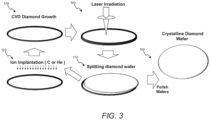
FIG. 3 provides perspective views of the seed wafer at various stages of theFIG. 1 process. -
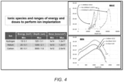
FIG. 4 depicts ionic species and respective energy ranges, dosage ranges, and depths at the depicted maximum and minimum dosages. -
FIG. 5 depicts ionic species and respective energy ranges, dosage ranges, damage in vacancies at the depicted maximum dosages. - The following discussion provides various examples of providing diamond wafers or films. Such examples are non-limiting, and the scope of the appended claims should not be limited to the particular examples disclosed. In the following discussion, the terms "example" and "e.g." are non-limiting.
- The figures illustrate the general manner of construction, and descriptions and details of well-known features and techniques may be omitted to avoid unnecessarily obscuring the present disclosure. In addition, elements in the drawing figures are not necessarily drawn to scale. For example, the dimensions of some of the elements in the figures may be exaggerated relative to other elements to help improve understanding of the examples discussed in the present disclosure. The same reference numerals in different figures denote the same elements.
- The term "and/or" means any one or more of the items in the list joined by "and/or". As an example, "x and/or y" means any element of the three-element set {(x), (y), (x, y)}. As another example, "x, y, and/or z" means any element of the seven-element set {(x), (y), (z), (x, y), (x, z), (y, z), (x, y, z)}.
- The terms "comprises," "comprising," "includes," and/or "including," are "open ended" terms and specify the presence of stated features, but do not preclude the presence or addition of one or more other features.
- The terms "first," "second," etc. may be used herein to describe various elements, and these elements should not be limited by these terms. These terms are only used to distinguish one element from another. Thus, for example, a first element discussed in this disclosure could be termed a second element without departing from the teachings of the present disclosure.
- Unless specified otherwise, the term "coupled" may be used to describe two elements directly contacting each other or describe two elements indirectly connected by one or more other elements. For example, if element A is coupled to element B, then element A can be directly contacting element B or indirectly connected to element B by an intervening element C. Similarly, the terms "over" or "on" may be used to describe two elements directly contacting each other or describe two elements indirectly connected by one or more other elements.
- Generally, aspects of the present disclosure are directed to processes for forming crystalline wafers or films. Such a process may include creating a damaged layer in a seed wafer at a depth from a seed wafer upper surface and forming a crystalline structure on the seed wafer upper surface. The method may also include applying light from a laser to the damaged layer to separate the formed crystalline structure from the seed wafer and obtain the wafer. More specifically, the seed wafer may include a diamond crystalline structure. The forming of the crystalline structure may include growing a diamond epitaxial layer on the seed wafer upper surface via a chemical vapor deposition (CVD) process. A growth temperature of the CVD process may convert the damaged layer into a graphitized interface between the seed wafer and the diamond epitaxial layer. Applying the light from the laser may separate the diamond epitaxial layer from the seed wafer to obtain a diamond wafer.
- Referring now to
FIGS. 1-3 , aprocess 100 of forming diamond wafers or films is shown. While theprocess 100 is shown and described below specifically in regard to forming diamond wafers or films, theprocess 100 may be used to form wafers or films of crystalline materials other than diamond. At 110, aseed wafer 10 is prepared for ion implantation. Theseed wafer 10 may comprise a seed waferupper surface 12, a seed waferlower surface 14, and a seed waferlateral surface 16 between the seed waferupper surface 12 and the seed waferlower surface 14. At 110, the seed waferupper surface 12 may be polished to remove surface defects in the diamond crystalline structure of theseed wafer 10. - At 120, a damaged
layer 20 may be created below the seed waferupper surface 12. To this end,ions 22 may be implanted to a desired depth D in theseed wafer 10 via the seed waferupper surface 12. Such implanting may damage the diamond crystalline structure and creating bond vacancies in the diamond crystalline structure of theseed wafer 10. Various ionic species may be implanted. In particular, hydrogen, helium, and/or carbon ions may be implanted via the seed waferupper surface 12 to a depth below the seed waferupper surface 12 that is dependent upon the ionic species and the implantation energy. - As shown in the table of
FIG. 4 , hydrogen ions may be implanted using an implant energy ranging from 20 kiloelectronvolts (keV) to 525 keV, which respectively correspond to a peak concentration implantation depth between 0.1 microns (µm) and 3.0 µm into the diamond crystalline structure of theseed wafer 10. Similarly, helium ions may be implanted using an implant energy ranging from 20 keV to 1220 keV, which respectively correspond to a peak concentration implantation depth of between 0.2 µm and 2.0 µm into the diamond crystalline structure of theseed wafer 10. Further, carbon ions may be implanted using an implant energy ranging from 80 keV to 1220 keV, which respectively correspond to a peak concentration implantation depth of between 0.1 µm and 1.6 µm into the diamond crystalline structure of theseed wafer 10. -
FIG. 4 further provides a first graph of concentration versus depth of the hydrogen, helium, and carbon ion species at their respective maximum ion implantation energies and maximum dosages noted in the table.FIG. 4 further provides a second graph of concentration versus depth of the hydrogen, helium, and carbon ion species at their respective minimum ion implantation energies and minimum dosages noted in the table. The graphs are based on simulation data. - As further shown in
FIG. 5 , the concentration of vacant bonds at the implantation depth is dependent upon the implantation dosage of the various ion species. In particular, hydrogen ions may be implanted at a dosage ranging between 1e14 ions/cm2 to 1.2e17 ions/cm2. Helium ions may be implanted at a dosage ranging between 1e13 ions/cm2 to 1.2e17. Carbon ions may be implanted at a dosage ranging between 1e12 and 2.0e16. The graph ofFIG. 5 depicts vacancies versus implantation depth for carbon ions and helium ions at their respective listed maximum implantation energies and dosages. As shown, implantation energies and dosages may result in peak vacancies of roughly 2.5e23 per cubic centimeter. Again, the graph is based on simulation data. - At 130, the
process 100 grows anepitaxial layer 30 on theseed wafer 10. To this end, theprocess 100 may use a crystal growth process suitable for growing anepitaxial layer 30 of diamond on the seed waferupper surface 12. Such growth may result in the formation of grains whose crystalline structure aligns with the crystalline structure ofseed wafer 10 and continues such crystalline structure beyond the seed waferupper surface 12. - In various embodiments, a chemical vapor deposition (CVD) process may be used to grow the
epitaxial layer 30. Such a CVD process may be conducted at growth temperatures (e.g., 1100-1150 °C) that are sufficient to anneal the damagedlayer 20 and convert the damagedlayer 20 into graphite. Such conversion to graphite effectively provides agraphitized interface 24 between the diamond crystalline structure of theseed wafer 10 and the diamond crystalline structure of theepitaxial layer 30. - After forming the
epitaxial layer 30 and forming thegraphitized interface 24, theprocess 100 at 140 may separate theepitaxial layer 30 from theseed wafer 10. To this end, theprocess 100 may include focusing light emitted from alaser 50 on thegraphitized interface 24 to break bonds of the graphitizedinterface 24 and separate theepitaxial layer 30 from theseed wafer 10. In various embodiments, thegraphitized interface 24 provides an opaque layer in the otherwise transparent structure. Due to the opaque nature of the graphitizedinterface 24, thelaser 50 may be absorbed by the graphitizedinterface 24 and break bonds of the graphitizedinterface 24. As such, the effects of thelaser 50 may be localized to the graphitizedinterface 24 and thus avoid further damaging the crystalline structure of theepitaxial layer 30 and/orseed wafer 10. - At 150, the
process 100 may output a new diamond wafer or film by finish processing of the separatedepitaxial layer 30. In particular, theprocess 100 may polish and/or etch a lower side of the separatedepitaxial layer 30 to remove remnants of the graphitizedinterface 24. Such polishing and/or etching may also remove and/or reduce defects along the graphitizedinterface 24. - As shown in
FIGS. 2 and3 , theprocess 100 may be repeated and theseed wafer 10 may be reused. - In the following, a set of aspects is disclosed. The aspects are numbered to facilitate referencing the features of one aspect in other aspects. The aspects form part of the disclosure of the present application and could be made subject to independent and/or dependent claims irrespective of what currently is claimed in the application. The aspects are:
- 1. A method of forming a wafer, the method comprising:
- creating a damaged layer in a seed wafer at a depth from a seed wafer upper surface;
- forming a crystalline structure on the seed wafer upper surface; and
- applying light from a laser to the damaged layer to separate the formed crystalline structure from the seed wafer and obtain the wafer.
- 2. The method of
aspect 1, wherein creating the damaged layer comprises implanting ions into the seed wafer via the seed wafer upper surface. - 3. The method of
aspect 1, wherein creating the damaged layer comprises implanting helium ions into the seed wafer via the seed wafer upper surface. - 4. The method of
aspect 1, wherein creating the damaged layer comprises implanting hydrogen ions into the seed wafer via the seed wafer upper surface. - 5. The method of
aspect 1, wherein creating the damaged layer comprises implanting carbon ions into the seed wafer via the seed wafer upper surface. - 6. The method of
aspect 1, wherein forming the crystalline structure comprising growing an epitaxial layer on the seed wafer upper surface. - 7. The method of aspect 6, wherein growing the epitaxial layer comprises using a chemical vapor deposition (CVD) process to grow the epitaxial layer.
- 8. The method of aspect 7, wherein a growth temperature of the CVD process anneals the damaged layer.
- 9. The method of aspect 7, wherein a growth temperature of the CVD process converts the damaged layer into graphite and forms a graphitized interface between the epitaxial layer and the seed wafer.
- 10. The method of
aspect 1, comprising removing remnants of the damaged layer from the wafer. - 11. The method of
aspect 1, comprising polishing a lower surface of the wafer. - 12. The method of
aspect 1, comprising etching a lower surface of the wafer. - 13. The method of
aspect 1, comprising reusing the seed wafer, after separating the wafer from the seed wafer, to form another wafer. - 14. The method of
aspect 1, wherein:- the seed wafer comprises a diamond crystalline structure; and
- the wafer separated from the seed wafer comprises a diamond crystalline structure.
- 15. A method of forming a diamond wafer, the method comprising:
- creating a damaged layer in a seed wafer at a depth from a seed wafer upper surface, wherein the seed wafer comprises a diamond crystalline structure;
- growing a diamond epitaxial layer on the seed wafer upper surface via a chemical vapor deposition (CVD) process, wherein a growth temperature of the CVD process converts the damaged layer into a graphitized interface between the seed wafer and the diamond epitaxial layer; and
- applying light from a laser to the graphitized interface to separate the diamond epitaxial layer from the seed wafer and obtain the diamond wafer.
- 16. The method of
aspect 15, wherein creating the damaged layer comprises implanting ions into the seed wafer via the seed wafer upper surface. - 17. The method of
aspect 16, wherein the ions include helium, hydrogen, and/or carbon ions. - 18. The method of
aspect 15, comprising removing remnants of the graphitized interface from the diamond wafer. - 19. The method of
aspect 15, comprising polishing a lower surface of the diamond wafer. - 20. The method of
aspect 15, comprising etching a lower surface of the diamond wafer. - Implementations as described herein may relate to the following: Methods of forming a crystalline wafers or films such as a diamond wafer or film. Such a method may include creating a damaged layer in a seed wafer at a depth from a seed wafer upper surface. The seed wafer may include a diamond crystalline structure. The method may also include growing a diamond epitaxial layer on the seed wafer upper surface via a chemical vapor deposition (CVD) process. A growth temperature of the CVD process may convert the damaged layer into a graphitized interface between the seed wafer and the diamond epitaxial layer. The method may further include applying light from a laser to the graphitized interface to separate the diamond epitaxial layer from the seed wafer and obtain the diamond wafer.
- The present application claims priority of
U.S. Patent Application No. 63/594,544, filed October 31, 2023 U.S. Patent Application No. 18/433,031, filed February 5, 2024 - The present disclosure includes reference to certain examples, however, it will be understood by those skilled in the art that various changes may be made and equivalents may be substituted without departing from the scope of the disclosure. In addition, modifications may be made to the disclosed examples without departing from the scope of the present disclosure. Therefore, it is intended that the present disclosure not be limited to the examples disclosed, but that the disclosure will include all examples falling within the scope of the appended claims.
Claims (15)
- A method of forming a wafer, the method comprising:creating a damaged layer in a seed wafer at a depth from a seed wafer upper surface;forming a crystalline structure on the seed wafer upper surface; andapplying light from a laser to the damaged layer to separate the formed crystalline structure from the seed wafer and obtain the wafer.
- The method of claim 1, wherein creating the damaged layer comprises implanting ions into the seed wafer via the seed wafer upper surface.
- The method of claim 1 or 2, wherein creating the damaged layer comprises implanting helium ions into the seed wafer via the seed wafer upper surface.
- The method of any one of claims 1 to 3, wherein creating the damaged layer comprises implanting hydrogen ions into the seed wafer via the seed wafer upper surface.
- The method of any one of claims 1 to 4, wherein creating the damaged layer comprises implanting carbon ions into the seed wafer via the seed wafer upper surface.
- The method of any one of claims 1 to 5, wherein forming the crystalline structure comprises growing an epitaxial layer on the seed wafer upper surface.
- The method of claim 6, wherein growing the epitaxial layer comprises using a chemical vapor deposition (CVD) process to grow the epitaxial layer.
- The method of claim 7, wherein a growth temperature of the CVD process anneals the damaged layer.
- The method of claim 7, wherein a growth temperature of the CVD process converts the damaged layer into graphite and forms a graphitized interface between the epitaxial layer and the seed wafer.
- The method of any one of claims 1 to 9, comprising removing remnants of the damaged layer from the wafer.
- The method of any one of claims 1 to 10, comprisinga) polishing a lower surface of the wafer, and/orb) comprising etching a lower surface of the wafer.
- The method of any one of claims 1 to 11, comprising reusing the seed wafer, after separating the wafer from the seed wafer, to form another wafer.
- The method of any one of claims 1 to 12, wherein:the seed wafer comprises a diamond crystalline structure; andthe wafer separated from the seed wafer comprises a diamond crystalline structure.
- A method of forming a diamond wafer, the method comprising:creating a damaged layer in a seed wafer at a depth from a seed wafer upper surface, wherein the seed wafer comprises a diamond crystalline structure;growing a diamond epitaxial layer on the seed wafer upper surface via a chemical vapor deposition (CVD) process, wherein a growth temperature of the CVD process converts the damaged layer into a graphitized interface between the seed wafer and the diamond epitaxial layer; andapplying light from a laser to the graphitized interface to separate the diamond epitaxial layer from the seed wafer and obtain the diamond wafer.
- The method of claim 14, whereina) creating the damaged layer comprises implanting ions into the seed wafer via the seed wafer upper surface, and optionally wherein the ions include helium, hydrogen, and/or carbon ions, and/or wherein the method further comprises:b) removing remnants of the graphitized interface from the diamond wafer, and/orc) polishing a lower surface of the diamond wafer, and/ord) etching a lower surface of the diamond wafer.
Applications Claiming Priority (2)
| Application Number | Priority Date | Filing Date | Title |
|---|---|---|---|
| US202363594544P | 2023-10-31 | 2023-10-31 | |
| US18/433,031 US12696692B2 (en) | 2023-10-31 | 2024-02-05 | Crystalline wafers and process for forming crystalline wafers |
Publications (1)
| Publication Number | Publication Date |
|---|---|
| EP4549637A1 true EP4549637A1 (en) | 2025-05-07 |
Family
ID=92538898
Family Applications (1)
| Application Number | Title | Priority Date | Filing Date |
|---|---|---|---|
| EP24196250.5A Pending EP4549637A1 (en) | 2023-10-31 | 2024-08-23 | Crystalline wafers and process for forming crystalline wafers |
Country Status (4)
| Country | Link |
|---|---|
| US (1) | US12696692B2 (en) |
| EP (1) | EP4549637A1 (en) |
| JP (1) | JP7787230B2 (en) |
| KR (1) | KR102996813B1 (en) |
Citations (1)
| Publication number | Priority date | Publication date | Assignee | Title |
|---|---|---|---|---|
| US20170233889A1 (en) * | 2014-08-08 | 2017-08-17 | Sumitomo Electric Industries, Ltd. | Method of manufacturing diamond, diamond, diamond composite substrate, diamond joined substrate, and tool |
Family Cites Families (12)
| Publication number | Priority date | Publication date | Assignee | Title |
|---|---|---|---|---|
| US5334283A (en) | 1992-08-31 | 1994-08-02 | The University Of North Carolina At Chapel Hill | Process for selectively etching diamond |
| GB0127263D0 (en) | 2001-11-13 | 2002-01-02 | Diamanx Products Ltd | Layered structures |
| JP4694144B2 (en) | 2004-05-14 | 2011-06-08 | 住友電気工業株式会社 | Method for growing SiC single crystal and SiC single crystal grown thereby |
| JP4873467B2 (en) | 2006-07-27 | 2012-02-08 | 独立行政法人産業技術総合研究所 | Method for manufacturing single crystal substrate having off-angle |
| US7943485B2 (en) * | 2007-01-22 | 2011-05-17 | Group4 Labs, Llc | Composite wafers having bulk-quality semiconductor layers and method of manufacturing thereof |
| JP4803464B2 (en) | 2008-07-04 | 2011-10-26 | 独立行政法人産業技術総合研究所 | Method for removing surface damage of single crystal diamond |
| KR101310546B1 (en) | 2008-08-29 | 2013-09-23 | 신닛테츠스미킨 카부시키카이샤 | Manufacturing method for silicon carbide monocrystals |
| US7968401B2 (en) * | 2009-01-26 | 2011-06-28 | Applied Materials, Inc. | Reducing photoresist layer degradation in plasma immersion ion implantation |
| JP5540296B2 (en) | 2010-10-13 | 2014-07-02 | 独立行政法人産業技術総合研究所 | Diamond electronic device and manufacturing method thereof |
| JP2012086988A (en) | 2010-10-15 | 2012-05-10 | Sumitomo Electric Ind Ltd | Process for exfoliating diamond |
| JP5382742B2 (en) | 2011-10-20 | 2014-01-08 | 独立行政法人産業技術総合研究所 | Method for manufacturing single crystal substrate having off-angle |
| CN107400871A (en) * | 2017-07-28 | 2017-11-28 | 西安交通大学 | A kind of preparation method of the diamond thin based on silicon substrate |
-
2024
- 2024-02-05 US US18/433,031 patent/US12696692B2/en active Active
- 2024-05-30 JP JP2024087912A patent/JP7787230B2/en active Active
- 2024-07-11 KR KR1020240091784A patent/KR102996813B1/en active Active
- 2024-08-23 EP EP24196250.5A patent/EP4549637A1/en active Pending
Patent Citations (1)
| Publication number | Priority date | Publication date | Assignee | Title |
|---|---|---|---|---|
| US20170233889A1 (en) * | 2014-08-08 | 2017-08-17 | Sumitomo Electric Industries, Ltd. | Method of manufacturing diamond, diamond, diamond composite substrate, diamond joined substrate, and tool |
Also Published As
| Publication number | Publication date |
|---|---|
| US12696692B2 (en) | 2026-07-28 |
| US20250140556A1 (en) | 2025-05-01 |
| JP2025076262A (en) | 2025-05-15 |
| KR20250063148A (en) | 2025-05-08 |
| KR102996813B1 (en) | 2026-07-29 |
| JP7787230B2 (en) | 2025-12-16 |
Similar Documents
| Publication | Publication Date | Title |
|---|---|---|
| US10683588B2 (en) | Shaped silicon ingot using layer transfer | |
| US7910458B2 (en) | Method and structure using selected implant angles using a linear accelerator process for manufacture of free standing films of materials | |
| EP2879176B1 (en) | Method for producing hybrid substrates, and hybrid substrate | |
| JP2005047792A (en) | Microstructure, in particular heteroepitaxial microstructure and method therefor | |
| US20170338143A1 (en) | A method of manufacturing high resistivity semiconductor-on-insulator wafers with charge trapping layers | |
| JP2010219566A (en) | Method for transferring thin layers of monocrystalline material onto desirable substrate | |
| TWI850519B (en) | PROCESS FOR MANUFACTURING A COMPOSITE STRUCTURE COMPRISING A THIN LAYER MADE OF MONOCRYSTALLINESIC ON A CARRIER SUBSTRATE MADE OF SiC | |
| US12476149B2 (en) | Crystal efficient SiC device wafer production | |
| CN1371434A (en) | Slicing of single-crystal films using ion implantation | |
| JP7594585B2 (en) | Process for producing a composite structure comprising a thin layer of monocrystalline SiC on a carrier substrate made of SiC | |
| EP2879177B1 (en) | Method for producing sos substrates, and sos substrate | |
| CN101809710B (en) | Method of manufacturing a structure comprising a substrate and a layer deposited on one surface of the substrate | |
| US20250140556A1 (en) | Crystalline wafers and process for forming crystalline wafers | |
| US10475696B2 (en) | Method of manufacture of a semiconductor on insulator structure | |
| EP1437764A1 (en) | A compliant substrate for a heteroepitaxy, a heteroepitaxial structure and a method for fabricating a compliant substrate | |
| CN119400756A (en) | A method for preparing semiconductor material and device | |
| EP4586304A1 (en) | Implantation process to mitigate bowing of wafers introduced by splitting process | |
| TWI861253B (en) | PROCESS FOR MANUFACTURING A COMPOSITE STRUCTURE COMPRISING A THIN LAYER OF MONOCRYSTALLINE SiC ON A CARRIER SUBSTRATE MADE OF SiC | |
| CN1796620A (en) | Internally gettered heteroepitaxial semiconductor wafers and methods of manufacturing such wafers | |
| TW202036657A (en) | A method to make membrane on a substrate |
Legal Events
| Date | Code | Title | Description |
|---|---|---|---|
| PUAI | Public reference made under article 153(3) epc to a published international application that has entered the european phase |
Free format text: ORIGINAL CODE: 0009012 |
|
| STAA | Information on the status of an ep patent application or granted ep patent |
Free format text: STATUS: REQUEST FOR EXAMINATION WAS MADE |
|
| 17P | Request for examination filed |
Effective date: 20240823 |
|
| AK | Designated contracting states |
Kind code of ref document: A1 Designated state(s): AL AT BE BG CH CY CZ DE DK EE ES FI FR GB GR HR HU IE IS IT LI LT LU LV MC ME MK MT NL NO PL PT RO RS SE SI SK SM TR |
|
| P01 | Opt-out of the competence of the unified patent court (upc) registered |
Free format text: CASE NUMBER: APP_22320/2025 Effective date: 20250512 |