EP4549372A1 - Micro-electro-mechanical device having contact pads that are protected against humidity and manufacturing process thereof - Google Patents
Micro-electro-mechanical device having contact pads that are protected against humidity and manufacturing process thereof Download PDFInfo
- Publication number
- EP4549372A1 EP4549372A1 EP24209213.8A EP24209213A EP4549372A1 EP 4549372 A1 EP4549372 A1 EP 4549372A1 EP 24209213 A EP24209213 A EP 24209213A EP 4549372 A1 EP4549372 A1 EP 4549372A1
- Authority
- EP
- European Patent Office
- Prior art keywords
- structural layer
- regions
- connection
- structures
- forming
- Prior art date
- Legal status (The legal status is an assumption and is not a legal conclusion. Google has not performed a legal analysis and makes no representation as to the accuracy of the status listed.)
- Pending
Links
Images


Classifications
-
- B—PERFORMING OPERATIONS; TRANSPORTING
- B81—MICROSTRUCTURAL TECHNOLOGY
- B81B—MICROSTRUCTURAL DEVICES OR SYSTEMS, e.g. MICROMECHANICAL DEVICES
- B81B7/00—Microstructural systems ; Auxiliary parts of microstructural devices or systems
- B81B7/0032—Packages or encapsulation
- B81B7/0035—Packages or encapsulation for maintaining a controlled atmosphere inside of the chamber containing the MEMS
- B81B7/0038—Packages or encapsulation for maintaining a controlled atmosphere inside of the chamber containing the MEMS using materials for controlling the level of pressure, contaminants or moisture inside of the package, e.g. getters
-
- B—PERFORMING OPERATIONS; TRANSPORTING
- B81—MICROSTRUCTURAL TECHNOLOGY
- B81B—MICROSTRUCTURAL DEVICES OR SYSTEMS, e.g. MICROMECHANICAL DEVICES
- B81B7/00—Microstructural systems ; Auxiliary parts of microstructural devices or systems
- B81B7/0032—Packages or encapsulation
- B81B7/007—Interconnections between the MEMS and external electrical signals
-
- B—PERFORMING OPERATIONS; TRANSPORTING
- B81—MICROSTRUCTURAL TECHNOLOGY
- B81B—MICROSTRUCTURAL DEVICES OR SYSTEMS, e.g. MICROMECHANICAL DEVICES
- B81B7/00—Microstructural systems ; Auxiliary parts of microstructural devices or systems
- B81B7/0032—Packages or encapsulation
- B81B7/0064—Packages or encapsulation for protecting against electromagnetic or electrostatic interferences
-
- B—PERFORMING OPERATIONS; TRANSPORTING
- B81—MICROSTRUCTURAL TECHNOLOGY
- B81C—PROCESSES OR APPARATUS SPECIALLY ADAPTED FOR THE MANUFACTURE OR TREATMENT OF MICROSTRUCTURAL DEVICES OR SYSTEMS
- B81C1/00—Manufacture or treatment of devices or systems in or on a substrate
- B81C1/00015—Manufacture or treatment of devices or systems in or on a substrate for manufacturing microsystems
- B81C1/00261—Processes for packaging MEMS devices
- B81C1/00277—Processes for packaging MEMS devices for maintaining a controlled atmosphere inside of the cavity containing the MEMS
- B81C1/00285—Processes for packaging MEMS devices for maintaining a controlled atmosphere inside of the cavity containing the MEMS using materials for controlling the level of pressure, contaminants or moisture inside of the package, e.g. getters
-
- B—PERFORMING OPERATIONS; TRANSPORTING
- B81—MICROSTRUCTURAL TECHNOLOGY
- B81B—MICROSTRUCTURAL DEVICES OR SYSTEMS, e.g. MICROMECHANICAL DEVICES
- B81B2201/00—Specific applications of microelectromechanical systems
- B81B2201/02—Sensors
- B81B2201/0228—Inertial sensors
- B81B2201/0235—Accelerometers
-
- B—PERFORMING OPERATIONS; TRANSPORTING
- B81—MICROSTRUCTURAL TECHNOLOGY
- B81B—MICROSTRUCTURAL DEVICES OR SYSTEMS, e.g. MICROMECHANICAL DEVICES
- B81B2201/00—Specific applications of microelectromechanical systems
- B81B2201/02—Sensors
- B81B2201/0228—Inertial sensors
- B81B2201/0242—Gyroscopes
-
- B—PERFORMING OPERATIONS; TRANSPORTING
- B81—MICROSTRUCTURAL TECHNOLOGY
- B81B—MICROSTRUCTURAL DEVICES OR SYSTEMS, e.g. MICROMECHANICAL DEVICES
- B81B2203/00—Basic microelectromechanical structures
- B81B2203/04—Electrodes
-
- B—PERFORMING OPERATIONS; TRANSPORTING
- B81—MICROSTRUCTURAL TECHNOLOGY
- B81B—MICROSTRUCTURAL DEVICES OR SYSTEMS, e.g. MICROMECHANICAL DEVICES
- B81B2207/00—Microstructural systems or auxiliary parts thereof
- B81B2207/07—Interconnects
-
- B—PERFORMING OPERATIONS; TRANSPORTING
- B81—MICROSTRUCTURAL TECHNOLOGY
- B81B—MICROSTRUCTURAL DEVICES OR SYSTEMS, e.g. MICROMECHANICAL DEVICES
- B81B2207/00—Microstructural systems or auxiliary parts thereof
- B81B2207/09—Packages
- B81B2207/091—Arrangements for connecting external electrical signals to mechanical structures inside the package
- B81B2207/097—Interconnects arranged on the substrate or the lid, and covered by the package seal
-
- B—PERFORMING OPERATIONS; TRANSPORTING
- B81—MICROSTRUCTURAL TECHNOLOGY
- B81C—PROCESSES OR APPARATUS SPECIALLY ADAPTED FOR THE MANUFACTURE OR TREATMENT OF MICROSTRUCTURAL DEVICES OR SYSTEMS
- B81C2201/00—Manufacture or treatment of microstructural devices or systems
- B81C2201/01—Manufacture or treatment of microstructural devices or systems in or on a substrate
- B81C2201/0101—Shaping material; Structuring the bulk substrate or layers on the substrate; Film patterning
- B81C2201/0102—Surface micromachining
- B81C2201/0105—Sacrificial layer
-
- B—PERFORMING OPERATIONS; TRANSPORTING
- B81—MICROSTRUCTURAL TECHNOLOGY
- B81C—PROCESSES OR APPARATUS SPECIALLY ADAPTED FOR THE MANUFACTURE OR TREATMENT OF MICROSTRUCTURAL DEVICES OR SYSTEMS
- B81C2201/00—Manufacture or treatment of microstructural devices or systems
- B81C2201/01—Manufacture or treatment of microstructural devices or systems in or on a substrate
- B81C2201/0101—Shaping material; Structuring the bulk substrate or layers on the substrate; Film patterning
- B81C2201/0118—Processes for the planarization of structures
- B81C2201/0123—Selective removal
-
- B—PERFORMING OPERATIONS; TRANSPORTING
- B81—MICROSTRUCTURAL TECHNOLOGY
- B81C—PROCESSES OR APPARATUS SPECIALLY ADAPTED FOR THE MANUFACTURE OR TREATMENT OF MICROSTRUCTURAL DEVICES OR SYSTEMS
- B81C2201/00—Manufacture or treatment of microstructural devices or systems
- B81C2201/01—Manufacture or treatment of microstructural devices or systems in or on a substrate
- B81C2201/0101—Shaping material; Structuring the bulk substrate or layers on the substrate; Film patterning
- B81C2201/0128—Processes for removing material
- B81C2201/013—Etching
- B81C2201/0132—Dry etching, i.e. plasma etching, barrel etching, reactive ion etching [RIE], sputter etching or ion milling
-
- B—PERFORMING OPERATIONS; TRANSPORTING
- B81—MICROSTRUCTURAL TECHNOLOGY
- B81C—PROCESSES OR APPARATUS SPECIALLY ADAPTED FOR THE MANUFACTURE OR TREATMENT OF MICROSTRUCTURAL DEVICES OR SYSTEMS
- B81C2201/00—Manufacture or treatment of microstructural devices or systems
- B81C2201/01—Manufacture or treatment of microstructural devices or systems in or on a substrate
- B81C2201/0101—Shaping material; Structuring the bulk substrate or layers on the substrate; Film patterning
- B81C2201/016—Passivation
Definitions
- the present invention relates to a micro-electromechanical device having contact pads protected against humidity and to the manufacturing process thereof.
- inertial-type MEMS devices of this type are increasingly used in consumer, automotive and industrial applications, they often integrate two or more inertial sensors in a same die and are packaged together with the related control circuits, generally formed in a separate die and forming an ASIC (Application Specific Integrated Circuit).
- ASIC Application Specific Integrated Circuit
- These devices are connected to the outside (for example to the ASIC and/or other external devices) through contact pads.
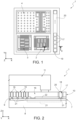
- Figure 1 shows, for example, an inertial-type MEMS device (hereinafter referred to as inertial device 1) forming a triaxial accelerometer, of capacitive type.
- inertial device 1 an inertial-type MEMS device (hereinafter referred to as inertial device 1) forming a triaxial accelerometer, of capacitive type.
- the inertial device 1 comprises a first sensitive portion 2, a second sensitive portion 3 and a third sensitive portion 4.
- the sensitive portions 2-4 include movable structures having a substantially planar extension, parallel to an XY plane of a Cartesian reference system XYZ.
- the first sensitive portion 2 is intended for detecting oscillations along a first horizontal axis X of the Cartesian reference system XYZ;
- the second sensitive portion 3 is intended for detecting oscillations along a second horizontal axis Y of the Cartesian reference system XYZ;
- the third sensitive portion 4 is intended for detecting oscillations along a vertical axis Z of the Cartesian reference system XYZ.
- the inertial MEMS device 2 may be formed in a die 7 of semiconductor material, comprising a substrate 8, for example of monocrystalline silicon; an insulating layer 9, superimposed on the substrate 7, for example of silicon oxide; a structural layer 10, superimposed on the insulating layer 9, for example of mono- or polycrystalline silicon; and a cap 11, for example of monocrystalline silicon, superimposed and attached to the structural layer 10.
- the structural layer 10 forms movable structures 15 (for example suspended masses and movable electrodes of the sensitive portions 2-4) and fixed structures 16 (for example fixed electrodes of the sensitive portions 2-4, a peripheral fixed structure and anchoring regions of the movable structures).
- movable structures 15 for example suspended masses and movable electrodes of the sensitive portions 2-4
- fixed structures 16 for example fixed electrodes of the sensitive portions 2-4, a peripheral fixed structure and anchoring regions of the movable structures.
- the movable structures 15 are suspended, at a distance, above the substrate 8 and the insulating layer 9 and extend at a distance from the cap 11 to be able to move freely or in a limited manner.
- connection structures 17 in a connection portion 19 ( Figure 1 ).
- the connection structures 17 are here columnar in shape, separated from each other and from the rest of the structural layer 10 by a trench 20, here shown empty, but which might be filled with material and layers that are at least partially insulating, so as to allow the electrical insulation thereof.
- Further conductive tracks may extend, at least in part, also on the structural layer 10, possibly electrically insulated therefrom by a dielectric layer, also not shown.
- Figure 2 further shows insulation regions 22 extending on the insulating layer 9, here in a peripheral region of the inertial device 1.
- the inertial device 1 After mounting on a connection support, for example a printed circuit board, and connecting the connection structures 17 to the external devices, lines and connectors, for example through wires not shown, the inertial device 1 is generally packaged in a protection housing, of insulating material, such as resin, in particular when they are intended to work in harsh environments.
- a protection housing of insulating material, such as resin, in particular when they are intended to work in harsh environments.
- the resin packages commonly used for the considered inertial devices are not completely hermetic and may allow passage of humidity, for example in presence of elaborate geometries and in proximity to the connection structures 17.
- the presence of humidity may affect the electrical characteristics of the devices and, above all, determine a variation thereof over time (drift phenomenon) which impacts the reliability of the inertial devices.
- connection structures 17 in particular between the structures connected to the movable masses (rotors) and the detection electrodes, affect the offset of the inertial device.
- these passive capacitances are calibrated during final test steps and the device parameters are trimmed to take into account the initial conditions.
- connection structures 17 in particular when manufactured using polycrystalline silicon deposition processes on sacrificial regions that are removed after the definition of the mechanical and electrical structures of the sensor, may cause penetration of humidity droplets during operation and considerably modify the electrical characteristics of the devices over time.
- Figure 3A also shows the packaging material, also called filler and indicated by 25, which covers the surface of the inertial device 1 and extends between the connection structures 17. Due to the current dimensions of the current structures (with structural layer 10 having a thickness of even 30 pm), the packaging material 25 may incorporate air or gas bubbles, indicated by 26 in Figure 3A . The air bubbles 26 prevent the filling material from completely filling the spaces between the connection structures 17 and may affect the resistivity and the capacitance between the connection structures 17, as represented schematically in Figure 3A by a resistance 27 and a capacitance 28.
- the packaging material 25 also called filler and indicated by 25
- the packaging material 25 may incorporate air or gas bubbles, indicated by 26 in Figure 3A .
- the air bubbles 26 prevent the filling material from completely filling the spaces between the connection structures 17 and may affect the resistivity and the capacitance between the connection structures 17, as represented schematically in Figure 3A by a resistance 27 and a capacitance 28.
- the inertial device 1 is calibrated so as to take into consideration the value of the resistance 27 and the capacitance 28.
- Figure 3B shows the presence of a water droplet 30 in contact with a connection structure 17.
- water drops may short-circuit two adjacent connection structures 17, especially in current devices wherein the structures are increasingly smaller and closer, and/or may cause current leakage, especially if they reach the conductive tracks 21.
- passivation structures may be created that completely surround the connection structures 17, for example by forming separate trenches that surround the individual connection structures 17, coating the trenches with a dielectric layer (for example a silicon oxide) and filling them with silicon.
- a dielectric layer for example a silicon oxide
- connection structures may be studied, with removal of the columnar regions formed in the structural layer, but this solution entails, in addition to additional manufacturing steps, lower flexibility in the design; therefore this solution is not always usable.
- DE102012200655B4 discloses a MEMS device having contact base formed by lower portions and upper portions that are mutually each other by trenches and protected at the top by an oxide layer.
- the aim of the present invention is to overcome the problem indicated above.
- a MEMS device a packaged device and a manufacturing process of a MEMS device are provided, as defined in the attached claims.
- a MEMS device comprising:
- connection portions of the connection structures may have a reduced height compared to prior art, so that it is less likely that air or gas bubbles, even of large dimensions, may touch two adjacent connection structures.
- any humidity that penetrates and infiltrates under any bubble that forms between two second connection portions cannot reach the conductive regions due to the height of the first connection portions.
- the lower height of the second connection portions with respect to the first connection portions of the connection structures causes the facing area of the second connection portions to be small, reducing the risk of electrical connection between adjacent second connection portions in case of humidity.
- FIG 4 shows a portion of a MEMS device 50.
- the MEMS device 50 is a generic device, for example the inertial device 1 of Figure 1 .
- the MEMS device 50 is a device made using two polycrystalline silicon layers and sacrificial material regions used for defining the device structures and selectively removed so as to free the movable structures, as described in Italian patent 102020000011755, filed on 5/20/2020 in the name of STMicroelectronics S.r.l, corresponding to the European patent application EP3912953A1 and the US patent application US210363000A1 .
- the MEMS device 50 is formed in a die 51 of semiconductor material, comprising a substrate 52, for example of monocrystalline silicon; an insulating layer 53, on the substrate 52, for example of silicon oxide; a first structural layer 54, on the insulating layer 53, of polycrystalline silicon; and a second structural layer 55, on the first structural layer 54, of polycrystalline silicon.
- a cap not shown for example of monocrystalline silicon, may be arranged on and attached to the second structural layer 54 in a zone thereof not visible in Figure 4 (see also the device of Figure 13 , where the cap is indicated by 87).
- the first and the second structural layers 54, 55 form movable structures and fixed structures, not shown, that form active structures (meaning therewith structures forming MEMS sensors/actuators).
- the structural layers 54, 55 form suspended masses, movable electrodes and fixed electrodes of the sensitive portions 2-4 of the inertial device 1 of Figure 1 (see also the device of Figure 13 , showing a first and a second sensitive portion 85, 86).
- the first structural layer 54 has a greater thickness than the second structural layer 55; for example, the first structural layer 54 may have a thickness comprised between 10 and 60 pm, in particular 20 ⁇ m, and the second structural layer 55 may have a thickness comprised between 5 and 20 pm, in particular of 8.4 ⁇ m.
- the first and the second structural layers 54, 55 also form a fixed peripheral region, including a connection portion 56 similar to the connection portion 19 of Figure 1 , wherein connection structures 57 shown in Figure 4 are formed (see also Figure 13 ).
- connection structure 57 (also referred to as pad) comprises a lower portion 57A, formed in/by the first structural layer 54, and an upper portion 57B, formed in/by the second structural layer 55.
- connection structures 57 Each lower portion 57A of the connection structures 57 is surrounded by an annular insulation region 58 of dielectric material, for example of silicon oxide, and are mutually separated by intermediate portions 59, also formed in/by the first structural layer 54.
- the intermediate portions 59 are therefore arranged between pairs of adjacent connection structures 57.
- the intermediate portions 59 are coupled here to the electrical ground of the device 50.
- Conductive regions 60 for example of doped polycrystalline silicon, extend above the insulating layer 53 and below the first structural layer 54, locally insulated therefrom by insulation portions 61.
- the conductive regions 60 are formed in a single layer and comprise here contact regions 60A, shielding regions 60B, first and second conductive tracks 60C' and 60C".
- the contact regions 60A are arranged below and in direct electrical contact with the lower portions 57A of the connection structures 57 at first contact areas 65.
- the contact regions 60A are formed in continuity and therefore electrically connected to the first conductive tracks 60C', as visible in Figure 5 .
- the first conductive tracks 60C' are connected to respective active structures (not shown) of the MEMS device 50, for example to suspended masses, rotors, movable electrodes or fixed electrodes of the sensitive portions (for example 85, 86 in Figure 13 ) and therefore form, with the connection structures 57, electrical connections of the active or MEMS structures 50 of the MEMS device 50 with the outside.
- the shielding regions 60B are arranged below and in direct electrical contact with the intermediate portions 59 of the first structural layer 54 at second contact areas 66 and are therefore also grounded. Furthermore, the shielding regions 60B are formed in continuity with and therefore electrically connected to the second conductive tracks 60C", as visible in Figure 5 .
- the second conductive tracks 60C are coupled with the parts connected to ground of the MEMS device 50 (for example, to the non-biased movable or fixed electrodes through the contact structures 57).
- one of the contact structures 57 might allow the ground of the device to be provided to the outside.
- the shielding regions 60B surround at a distance the contact regions 60A and are insulated therefrom by some of the insulation portions 61.
- the shielding regions 60B here have an open annular shape for the passage of the first conductive tracks 60C', as shown in Figure 5 .
- the shielding regions 60B are therefore electrically insulated with respect to the contact regions 60A and the first conductive tracks 60C' and shield the contact regions 60A, avoiding or at least limiting parasitic effects and leakage.
- the insulation portions 61 may be part of a sacrificial insulation layer, interrupted at the first and the second contact areas 65, 66.
- Figure 5 An embodiment of the conductive regions 60 is shown in Figure 5 , wherein the lower portions 57A of the connection structures 57 are not shown.
- Figure 5 shows the contact areas 65, 66, as well as the annular insulation region 58, and, with a dashed line, the boundaries of the contact regions 60A and the shielding regions 60B and part of the first and the second conductive tracks 60C' and 60C".
- the insulation layer forming the insulation portions 61 may be a first sacrificial layer used, during the manufacture of the MEMS device 50, for freeing suspended structures, as discussed in the aforementioned Italian patent 102020000011755 (removed for example in the sensitive portions 85 and 86 of Figure 13 ).
- a passivation layer 62 extends above the first structural layer 54.
- the passivation layer 62 also extends, in part, between the lower portion 57A and the upper portion 57B of each connection structure 57, as represented with a dashed line in Figure 6 , indicating the edge of an opening 88 of the passivation layer 62, wherein the first and the second structural layers 54, 55 are in direct contact.
- Soldering or welding regions 63 typically of metal such as aluminum Al, gold Au, copper Cu or aluminium-copper AlCu, extend above each connection structure 57, in direct contact with the upper portions 57B of the connection structures 57.
- connection structures 57 are mutually spaced, as also visible in the top-view of Figure 7 , showing a plurality of connection structures 57 and wherein, for ease of illustration, only the soldering regions 63 are shown with solid lines and the annular insulation regions 58, the contact regions 60A and the first conductive tracks 60C' of some connection structures 57 are shown with dashed lines.
- some packaging material 70 is molded, covers the connection structures 57 and fills the space between the upper portions 57B of the connection structures 57.
- connection structures 57 due to the reduced height of the second structural layer 55 and therefore of the upper portions 57B of the connection structures 57, compared to the structure of Figures 2 , 3A and 3B , it is less likely that air or gas bubbles 71, even of large dimensions, may touch two adjacent connection structures 57.
- the passivation layer 62, the annular insulation regions 58 and the insulation portions 61 form, as a whole, a tortuous, humidity stopping path.
- the lower height of the upper portions 57B with respect to the lower portions 57A of the connection structures 57 causes the facing area of the upper portions 57B to be smaller with respect to that of the lower portions 57A, reducing the risk of electrical connection in case of humidity.
- connection structures 57 that are grounded, form spacers which electrically separate the connection structures 57 from each other, avoiding parasitic couplings for most of their height and thus allowing to be placed very close to each other.
- the intermediate regions 59 avoid, during the packaging steps, an incomplete resin filling between the contact pads and therefore, as explained above, possible leakage between the contact pads in presence of humidity.
- connection structures 57 may be arranged so that their upper portions 57B and/or their lower portions 57A are distant at least 20 pm.
- the MEMS device 50 may be formed as shown in Figures 9-12 .
- Figure 9 shows a first wafer 80 of semiconductor material already subject to initial processing steps, as described in aforementioned Italian patent 102020000011755 .
- the first wafer 80 comprises the substrate 52, having the insulating layer 53 already formed thereon, for example thermally grown or deposited.
- the conductive regions 60 have been formed on the insulating layer 53, for example by deposition of a doped polycrystalline silicon layer and subsequent photolithographic definition.
- a first sacrificial layer (intended to form the insulation portions 61) of, for example, silicon oxide has been deposited and patterned above the conductive regions 60.
- the first sacrificial layer has been selectively removed above the conductive structures 60, where the contact areas 65, 66 are to be grown, as well as any other anchoring and electrical and/or mechanical connection portions where the electrical/mechanical connection is desired between the active structures of the MEMS device 50, formed in the first structural layer 54, and the substrate 50.
- the insulation portions 61 are therefore defined.
- the first structural layer 54 has already been grown, forming the contact areas 65, 66.
- the first structural layer 54 has already been etched, for example by dry etching, in the zones where for example the sensitive portions 85, 86 of Figure 13 are desired to be formed, forming trenches 68 which extend throughout the first structural layer 54 and define, i.a., the lower portions 57A of the connection structures 57 and the intermediate portions 59.
- a second sacrificial layer is deposited, forming also the passivation layer 62.
- the second sacrificial layer/passivation layer 62 is, for example, of TEOS (TetraEthylOrthoSilicate) having a thickness comprised, for example, between 0.1 ⁇ m and 5 ⁇ m.
- the second sacrificial layer/passivation layer 62 fills the trenches 68, forming, i.a., the annular insulation regions 58, is planarized and selectively removed, forming the passivation layer 62 and the openings 88.
- the second structural layer 55 is grown above the first structural layer 54 and the passivation layer 62.
- the second structural layer 54 is grown epitaxially and planarized, for example by CMP (Chemical Mechanical Polishing) so that, where the passivation layer 62 is not present (for example at the openings 88 in the connection portion 56), a structural layer is formed having a thickness equal to the sum of the thicknesses of the first and the second structural layers 54, 55.
- soldering regions 63 for example of AlCu, are formed.
- the soldering regions 63 may be formed by depositing and patterning a metal layer.
- the active structures of the MEMS device 50 formed by the sole second structural layer 55 or by both structural layers 54, 55 are defined, in particular for defining movable masses and fixed and movable electrodes of the sensitive portions 85, 96 of Figure 13 .
- the movable structures are released through selective removal of the first sacrificial layer 61, in a non-visible manner.
- a cap wafer is attached to the first wafer 80 through bonding regions 81 ( Figure 13 ); the first wafer 80 may be thinned, for example by lapping, so as to have a desired thickness; the cap wafer is cut, for example by dry etching, to open a window above the connection portion 56.
- Figure 12 again through a dry etching and using the soldering regions 63 as a mask, the second structural layer 55 is defined to form the upper portions 57B of the connection structures 57.
- the overall wafer is diced to form the inertial MEMS device 50.
- inertial MEMS device 50 thus obtainable is shown in Figure 13 , showing the connection portion 56 and an active portion 83 accommodating the first and the second sensitive portions 85, 86, similar to the sensitive portions 2 and 3 of Figure 1 .
- the first sensitive portion 85 is formed by the sole first structural layer 54 and the second sensitive portion 86 is formed by both structural layers 54, 55, but other active structures (meaning by this term structures forming MEMS sensors/actuators) might be formed in the sole second structural layer 55.
- Figure 13 shows the substrate 52; the first structural layer 54; the second structural layer 55; the passivation layer 62; the conductive regions 60; and the cap 87, covering the sensitive portions 85, 86 and bonded to the second structural layer 55.
- FIG. 13 Also shown in Figure 13 is a wire 90, soldered to one of the connection structures 57, and part of the packaging material 70, forming a packaged device 91.
- connection regions that may be reached, during use, by humidity and water droplets and might modify the electrical parameters of the same device in an undesired manner.
- the shielding regions 60B may be missing.
- the openings 88 above the lower portions 57A of the connection structures 57 may have a greater area than shown, for example approximately equal to that of the lower portions 57A, while maintaining electrical insulation between the upper portions 57B and the intermediate portions 59.
Landscapes
- Engineering & Computer Science (AREA)
- Microelectronics & Electronic Packaging (AREA)
- Computer Hardware Design (AREA)
- Manufacturing & Machinery (AREA)
- Physics & Mathematics (AREA)
- Electromagnetism (AREA)
- Micromachines (AREA)
Abstract
MEMS device (50) having a substrate (52) of semiconductor material; a first structural layer (54) of semiconductor material, on the substrate (52); a second structural layer (55) of semiconductor material, on the first structural layer (54); an active portion (83), accommodating active structures (85, 86) formed in the first structural layer (54) and/or in the second structural layer (55); a connection portion (56), accommodating a plurality of connection structures (57) and arranged laterally to the active portion (85, 86); and a plurality of conductive regions (60), arranged on the substrate (52) and extending between the active portion (85, 86) and the connection portion (56). Each connection structure (57) is formed by a first connection portion (57A), in electrical contact with a respective conductive region (60A) and formed in the first structural layer (54), and by a second connection portion (57B), on the first connection portion (57A) and in electrical continuity therewith, the second connection portion (57) formed in the second structural layer (55). The first connection portion (57A) has a greater thickness than the second connection portion (57B).
Description
- The present invention relates to a micro-electromechanical device having contact pads protected against humidity and to the manufacturing process thereof.
- In particular, the considered inertial MEMS device comprises one or more inertial sensors, such as an accelerometer and/or a gyroscope, formed in at least one silicon structural layer and defining at least one movable structure. The movable structure generally has main extension in an extension plane and is movable in-plane or out-of-plane.
- As known, inertial-type MEMS devices of this type are increasingly used in consumer, automotive and industrial applications, they often integrate two or more inertial sensors in a same die and are packaged together with the related control circuits, generally formed in a separate die and forming an ASIC (Application Specific Integrated Circuit).
- These devices are connected to the outside (for example to the ASIC and/or other external devices) through contact pads.
-
Figure 1 shows, for example, an inertial-type MEMS device (hereinafter referred to as inertial device 1) forming a triaxial accelerometer, of capacitive type. - The
inertial device 1 comprises a firstsensitive portion 2, a secondsensitive portion 3 and a thirdsensitive portion 4. The sensitive portions 2-4 include movable structures having a substantially planar extension, parallel to an XY plane of a Cartesian reference system XYZ. - In particular, in the shown
inertial device 1, the firstsensitive portion 2 is intended for detecting oscillations along a first horizontal axis X of the Cartesian reference system XYZ; the secondsensitive portion 3 is intended for detecting oscillations along a second horizontal axis Y of the Cartesian reference system XYZ; and the thirdsensitive portion 4 is intended for detecting oscillations along a vertical axis Z of the Cartesian reference system XYZ. - For example, as shown in the enlarged detail of
Figure 2 , theinertial MEMS device 2 may be formed in adie 7 of semiconductor material, comprising asubstrate 8, for example of monocrystalline silicon; aninsulating layer 9, superimposed on thesubstrate 7, for example of silicon oxide; astructural layer 10, superimposed on theinsulating layer 9, for example of mono- or polycrystalline silicon; and acap 11, for example of monocrystalline silicon, superimposed and attached to thestructural layer 10. - The
structural layer 10 forms movable structures 15 (for example suspended masses and movable electrodes of the sensitive portions 2-4) and fixed structures 16 (for example fixed electrodes of the sensitive portions 2-4, a peripheral fixed structure and anchoring regions of the movable structures). - The
movable structures 15 are suspended, at a distance, above thesubstrate 8 and theinsulating layer 9 and extend at a distance from thecap 11 to be able to move freely or in a limited manner. - The
structural layer 10 also formsconnection structures 17 in a connection portion 19 (Figure 1 ). The connection structures 17 (see alsoFigure 2 ) are here columnar in shape, separated from each other and from the rest of thestructural layer 10 by atrench 20, here shown empty, but which might be filled with material and layers that are at least partially insulating, so as to allow the electrical insulation thereof. - A
soldering layer 18, typically of metal such as aluminum Al, gold Au, copper Cu or aluminum-copper AlCu, extends on eachconnection structure 17. -
Conductive tracks 21, for example of doped polycrystalline silicon, extend above theinsulating layer 9, between thefixed structures 16 andrespective connection structures 17, for biasing the movable 15 andfixed structures 16 and for exchanging signals. - Further conductive tracks (not shown) may extend, at least in part, also on the
structural layer 10, possibly electrically insulated therefrom by a dielectric layer, also not shown. -
Figure 2 further showsinsulation regions 22 extending on theinsulating layer 9, here in a peripheral region of theinertial device 1. - After mounting on a connection support, for example a printed circuit board, and connecting the
connection structures 17 to the external devices, lines and connectors, for example through wires not shown, theinertial device 1 is generally packaged in a protection housing, of insulating material, such as resin, in particular when they are intended to work in harsh environments. - However, the resin packages commonly used for the considered inertial devices are not completely hermetic and may allow passage of humidity, for example in presence of elaborate geometries and in proximity to the
connection structures 17. However, the presence of humidity may affect the electrical characteristics of the devices and, above all, determine a variation thereof over time (drift phenomenon) which impacts the reliability of the inertial devices. - In fact, for example in accelerometers and in gyroscopes, the capacitances between the
connection structures 17, in particular between the structures connected to the movable masses (rotors) and the detection electrodes, affect the offset of the inertial device. - In these devices, these passive capacitances are calibrated during final test steps and the device parameters are trimmed to take into account the initial conditions.
- However, the current geometry and dimensions of the
connection structures 17, in particular when manufactured using polycrystalline silicon deposition processes on sacrificial regions that are removed after the definition of the mechanical and electrical structures of the sensor, may cause penetration of humidity droplets during operation and considerably modify the electrical characteristics of the devices over time. - For further understanding, reference be made to
Figure 3A , showing a section of theinertial device 1 in the zone of theconnection structures 17, through the same. -
Figure 3A also shows the packaging material, also called filler and indicated by 25, which covers the surface of theinertial device 1 and extends between theconnection structures 17. Due to the current dimensions of the current structures (withstructural layer 10 having a thickness of even 30 pm), thepackaging material 25 may incorporate air or gas bubbles, indicated by 26 inFigure 3A . Theair bubbles 26 prevent the filling material from completely filling the spaces between theconnection structures 17 and may affect the resistivity and the capacitance between theconnection structures 17, as represented schematically inFigure 3A by aresistance 27 and acapacitance 28. - As indicated, in the final test step, the
inertial device 1 is calibrated so as to take into consideration the value of theresistance 27 and thecapacitance 28. - However, during the life of the device, when exposed to humidity, tiny water droplets may penetrate inside the
packaging material 25, which is not hermetic, and modify the capacitance between twoconnection structures 17. - For example,
Figure 3B shows the presence of awater droplet 30 in contact with aconnection structure 17. - The presence of
water droplets 30 in the space between theconnection structures 17 not only modifies the capacitance between thesame connection structures 17, but may lead to catastrophic conditions for the device. - In fact, water drops may short-circuit two
adjacent connection structures 17, especially in current devices wherein the structures are increasingly smaller and closer, and/or may cause current leakage, especially if they reach theconductive tracks 21. - Since water drops cannot escape, this condition may only worsen over time, making inertial devices unreliable or even unusable.
- To overcome this issue, passivation structures may be created that completely surround the
connection structures 17, for example by forming separate trenches that surround theindividual connection structures 17, coating the trenches with a dielectric layer (for example a silicon oxide) and filling them with silicon. However, this solution entails an increase in the area necessary for theconnection structures 17, which clashes with the current trend to miniaturization. - Alternatively, in the final manufacturing step, different connection structures may be studied, with removal of the columnar regions formed in the structural layer, but this solution entails, in addition to additional manufacturing steps, lower flexibility in the design; therefore this solution is not always usable.
-
DE102012200655B4 discloses a MEMS device having contact base formed by lower portions and upper portions that are mutually each other by trenches and protected at the top by an oxide layer. - The aim of the present invention is to overcome the problem indicated above.
- According to the present invention, a MEMS device, a packaged device and a manufacturing process of a MEMS device are provided, as defined in the attached claims.
- In practice, a MEMS device is provided comprising:
- a substrate of semiconductor material;
- a first structural layer of semiconductor material, superimposed on the substrate and having a first thickness;
- a second structural layer of semiconductor material, superimposed on the first structural layer and having a second thickness;
- an active portion, accommodating active structures formed in the first structural layer and/or in the second structural layer;
- a connection portion, accommodating a plurality of connection structures and arranged laterally to the active portion; and
- a plurality of conductive regions, arranged above the substrate and extending between the active portion and the connection portion,
- wherein each connection structure comprises:
- a first connection portion, in electrical contact with a respective conductive region of the plurality of conductive regions and formed in the first structural layer; and
- a second connection portion, on the first connection portion and in electrical continuity therewith, the second connection portion formed in the second structural layer;
- the first connection portion having a greater thickness than the second connection portion.
- Thereby, the second connection portions of the connection structures may have a reduced height compared to prior art, so that it is less likely that air or gas bubbles, even of large dimensions, may touch two adjacent connection structures.
- In addition, any humidity that penetrates and infiltrates under any bubble that forms between two second connection portions cannot reach the conductive regions due to the height of the first connection portions.
- Furthermore, the lower height of the second connection portions with respect to the first connection portions of the connection structures causes the facing area of the second connection portions to be small, reducing the risk of electrical connection between adjacent second connection portions in case of humidity.
- For a better understanding of the present invention, embodiments thereof are now described, purely by way of nonlimiting example, with reference to the attached drawings, wherein:
-
Figure 1 is a top-plan view of a possible layout of an inertial MEMS device; -
Figure 2 is a cross-sectional view of a portion of the device ofFigure 1 , in the zone of the connection structures, taken along section line II-II ofFigure 1 ; -
Figures 3A and 3B show an enlarged detail of the zone of the connection structures ofFigure 2 , in presence of air bubbles and, respectively, water droplets; -
Figure 4 is a cross-sectional view of the present microelectromechanical device in the zone of the connection structures; -
Figure 5 is a cross-section taken along line V-V ofFigure 4 , illustrating the shape of a lower portion of a connection structure; -
Figure 6 is a top view of one of the connection structures ofFigure 4 ; -
Figure 7 is a top view of the zone of the connection structures of the microelectromechanical device ofFigure 4 ; -
Figure 8 is an enlarged cross-section of two connection structures of the microelectromechanical device ofFigure 4 , after packaging; -
Figures 9-12 are cross-sections, similar toFigure 8 , of a semiconductor wafer during successive manufacturing steps; and -
Figure 13 shows a cross-section of an embodiment of the present microelectromechanical device. - The following description refers to the arrangement shown; consequently, expressions such as "above", "below", "upper", "lower", "right", "left" relate to the attached figures and should not be interpreted in a limiting manner.
-
Figure 4 shows a portion of aMEMS device 50. TheMEMS device 50 is a generic device, for example theinertial device 1 ofFigure 1 . - The
MEMS device 50 is a device made using two polycrystalline silicon layers and sacrificial material regions used for defining the device structures and selectively removed so as to free the movable structures, as described inItalian patent 102020000011755, filed on 5/20/2020 EP3912953A1 and the US patent applicationUS210363000A1 . - In detail, the
MEMS device 50 is formed in adie 51 of semiconductor material, comprising asubstrate 52, for example of monocrystalline silicon; an insulatinglayer 53, on thesubstrate 52, for example of silicon oxide; a firststructural layer 54, on the insulatinglayer 53, of polycrystalline silicon; and a secondstructural layer 55, on the firststructural layer 54, of polycrystalline silicon. - A cap not shown, for example of monocrystalline silicon, may be arranged on and attached to the second
structural layer 54 in a zone thereof not visible inFigure 4 (see also the device ofFigure 13 , where the cap is indicated by 87). - The first and the second
structural layers structural layers inertial device 1 ofFigure 1 (see also the device ofFigure 13 , showing a first and a secondsensitive portion 85, 86). - The first
structural layer 54 has a greater thickness than the secondstructural layer 55; for example, the firststructural layer 54 may have a thickness comprised between 10 and 60 pm, in particular 20 µm, and the secondstructural layer 55 may have a thickness comprised between 5 and 20 pm, in particular of 8.4 µm. - The first and the second
structural layers connection portion 56 similar to theconnection portion 19 ofFigure 1 , whereinconnection structures 57 shown inFigure 4 are formed (see alsoFigure 13 ). - Each connection structure 57 (also referred to as pad) comprises a
lower portion 57A, formed in/by the firststructural layer 54, and anupper portion 57B, formed in/by the secondstructural layer 55. - Each
lower portion 57A of theconnection structures 57 is surrounded by anannular insulation region 58 of dielectric material, for example of silicon oxide, and are mutually separated byintermediate portions 59, also formed in/by the firststructural layer 54. Theintermediate portions 59 are therefore arranged between pairs ofadjacent connection structures 57. - The
intermediate portions 59 are coupled here to the electrical ground of thedevice 50. -
Conductive regions 60, for example of doped polycrystalline silicon, extend above the insulatinglayer 53 and below the firststructural layer 54, locally insulated therefrom byinsulation portions 61. - The
conductive regions 60 are formed in a single layer and comprise herecontact regions 60A, shieldingregions 60B, first and secondconductive tracks 60C' and 60C". - The
contact regions 60A are arranged below and in direct electrical contact with thelower portions 57A of theconnection structures 57 atfirst contact areas 65. - The
contact regions 60A are formed in continuity and therefore electrically connected to the firstconductive tracks 60C', as visible inFigure 5 . - The first
conductive tracks 60C', shown schematically inFigure 4 by dashed lines, are connected to respective active structures (not shown) of theMEMS device 50, for example to suspended masses, rotors, movable electrodes or fixed electrodes of the sensitive portions (for example 85, 86 inFigure 13 ) and therefore form, with theconnection structures 57, electrical connections of the active orMEMS structures 50 of theMEMS device 50 with the outside. - The shielding
regions 60B are arranged below and in direct electrical contact with theintermediate portions 59 of the firststructural layer 54 atsecond contact areas 66 and are therefore also grounded. Furthermore, the shieldingregions 60B are formed in continuity with and therefore electrically connected to the secondconductive tracks 60C", as visible inFigure 5 . - The second
conductive tracks 60C", shown schematically by dashed lines inFigure 4 , are coupled with the parts connected to ground of the MEMS device 50 (for example, to the non-biased movable or fixed electrodes through the contact structures 57). - Furthermore, one of the
contact structures 57 might allow the ground of the device to be provided to the outside. - The shielding
regions 60B surround at a distance thecontact regions 60A and are insulated therefrom by some of theinsulation portions 61. - The shielding
regions 60B here have an open annular shape for the passage of the firstconductive tracks 60C', as shown inFigure 5 . - The shielding
regions 60B are therefore electrically insulated with respect to thecontact regions 60A and the firstconductive tracks 60C' and shield thecontact regions 60A, avoiding or at least limiting parasitic effects and leakage. - For example, the
insulation portions 61 may be part of a sacrificial insulation layer, interrupted at the first and thesecond contact areas - An embodiment of the
conductive regions 60 is shown inFigure 5 , wherein thelower portions 57A of theconnection structures 57 are not shown. In particular,Figure 5 shows thecontact areas annular insulation region 58, and, with a dashed line, the boundaries of thecontact regions 60A and the shieldingregions 60B and part of the first and the secondconductive tracks 60C' and 60C". - With reference again to
Figure 4 , the insulation layer forming theinsulation portions 61 may be a first sacrificial layer used, during the manufacture of theMEMS device 50, for freeing suspended structures, as discussed in the aforementionedItalian patent 102020000011755 sensitive portions Figure 13 ). - A
passivation layer 62 extends above the firststructural layer 54. - Furthermore, here, the
passivation layer 62 also extends, in part, between thelower portion 57A and theupper portion 57B of eachconnection structure 57, as represented with a dashed line inFigure 6 , indicating the edge of anopening 88 of thepassivation layer 62, wherein the first and the secondstructural layers - In
Figure 4 , the portions of thepassivation layer 62 which extend between thelower portion 57A and theupper portion 57B of eachconnection structure 57 are indicated by 62A and contribute to preventing water or humidity droplets from reaching critical zones of thecontact structures 57, as explained hereinbelow. - Soldering or
welding regions 63, typically of metal such as aluminum Al, gold Au, copper Cu or aluminium-copper AlCu, extend above eachconnection structure 57, in direct contact with theupper portions 57B of theconnection structures 57. - The
upper portions 57B of theconnection structures 57 are mutually spaced, as also visible in the top-view ofFigure 7 , showing a plurality ofconnection structures 57 and wherein, for ease of illustration, only thesoldering regions 63 are shown with solid lines and theannular insulation regions 58, thecontact regions 60A and the firstconductive tracks 60C' of someconnection structures 57 are shown with dashed lines. - When the
MEMS device 50 is packaged, somepackaging material 70 is molded, covers theconnection structures 57 and fills the space between theupper portions 57B of theconnection structures 57. - In this situation, with reference to
Figure 8 , due to the reduced height of the secondstructural layer 55 and therefore of theupper portions 57B of theconnection structures 57, compared to the structure ofFigures 2 ,3A and 3B , it is less likely that air or gas bubbles 71, even of large dimensions, may touch twoadjacent connection structures 57. - In any case, any humidity that penetrates the
packaging material 70 and infiltrates under thebubble 71 formed between twoupper portions 57B, cannot reach theconductive regions 60, due to the height of the firststructural layer 54. - In addition, the
passivation layer 62, theannular insulation regions 58 and theinsulation portions 61 form, as a whole, a tortuous, humidity stopping path. - Furthermore, the lower height of the
upper portions 57B with respect to thelower portions 57A of theconnection structures 57 causes the facing area of theupper portions 57B to be smaller with respect to that of thelower portions 57A, reducing the risk of electrical connection in case of humidity. - The
intermediate regions 59 arranged betweenadjacent connection structures 57, that are grounded, form spacers which electrically separate theconnection structures 57 from each other, avoiding parasitic couplings for most of their height and thus allowing to be placed very close to each other. - Furthermore, the
intermediate regions 59 avoid, during the packaging steps, an incomplete resin filling between the contact pads and therefore, as explained above, possible leakage between the contact pads in presence of humidity. - For example, in this manner the
connection structures 57 may be arranged so that theirupper portions 57B and/or theirlower portions 57A are distant at least 20 pm. - The
MEMS device 50 may be formed as shown inFigures 9-12 . -
Figure 9 shows afirst wafer 80 of semiconductor material already subject to initial processing steps, as described in aforementionedItalian patent 102020000011755 - In particular, the
first wafer 80 comprises thesubstrate 52, having the insulatinglayer 53 already formed thereon, for example thermally grown or deposited. - The
conductive regions 60 have been formed on the insulatinglayer 53, for example by deposition of a doped polycrystalline silicon layer and subsequent photolithographic definition. - A first sacrificial layer (intended to form the insulation portions 61) of, for example, silicon oxide has been deposited and patterned above the
conductive regions 60. The first sacrificial layer has been selectively removed above theconductive structures 60, where thecontact areas MEMS device 50, formed in the firststructural layer 54, and thesubstrate 50. In this step, theinsulation portions 61 are therefore defined. - Furthermore, using an epitaxial growth process, the first
structural layer 54 has already been grown, forming thecontact areas - In
Figure 9 , the firststructural layer 54 has already been etched, for example by dry etching, in the zones where for example thesensitive portions Figure 13 are desired to be formed, formingtrenches 68 which extend throughout the firststructural layer 54 and define, i.a., thelower portions 57A of theconnection structures 57 and theintermediate portions 59. - In
Figure 10 , a second sacrificial layer is deposited, forming also thepassivation layer 62. The second sacrificial layer/passivation layer 62 is, for example, of TEOS (TetraEthylOrthoSilicate) having a thickness comprised, for example, between 0.1 µm and 5 µm. The second sacrificial layer/passivation layer 62 fills thetrenches 68, forming, i.a., theannular insulation regions 58, is planarized and selectively removed, forming thepassivation layer 62 and theopenings 88. - Then,
Figure 11 , the secondstructural layer 55 is grown above the firststructural layer 54 and thepassivation layer 62. The secondstructural layer 54 is grown epitaxially and planarized, for example by CMP (Chemical Mechanical Polishing) so that, where thepassivation layer 62 is not present (for example at theopenings 88 in the connection portion 56), a structural layer is formed having a thickness equal to the sum of the thicknesses of the first and the secondstructural layers - Then, the
soldering regions 63, for example of AlCu, are formed. - The
soldering regions 63 may be formed by depositing and patterning a metal layer. - Then, in a manner not shown, the active structures of the
MEMS device 50 formed by the sole secondstructural layer 55 or by bothstructural layers sensitive portions 85, 96 ofFigure 13 . - Subsequently, also in a manner not shown, the movable structures are released through selective removal of the first
sacrificial layer 61, in a non-visible manner. - Then, a cap wafer is attached to the
first wafer 80 through bonding regions 81 (Figure 13 ); thefirst wafer 80 may be thinned, for example by lapping, so as to have a desired thickness; the cap wafer is cut, for example by dry etching, to open a window above theconnection portion 56. In this step,Figure 12 , again through a dry etching and using thesoldering regions 63 as a mask, the secondstructural layer 55 is defined to form theupper portions 57B of theconnection structures 57. - Subsequently, the overall wafer is diced to form the
inertial MEMS device 50. - An example of
inertial MEMS device 50 thus obtainable is shown inFigure 13 , showing theconnection portion 56 and anactive portion 83 accommodating the first and the secondsensitive portions sensitive portions Figure 1 . Here, the firstsensitive portion 85 is formed by the sole firststructural layer 54 and the secondsensitive portion 86 is formed by bothstructural layers structural layer 55. - In detail,
Figure 13 shows thesubstrate 52; the firststructural layer 54; the secondstructural layer 55; thepassivation layer 62; theconductive regions 60; and thecap 87, covering thesensitive portions structural layer 55. - Also shown in
Figure 13 is awire 90, soldered to one of theconnection structures 57, and part of thepackaging material 70, forming a packageddevice 91. - Finally, it is clear that modifications and variations may be made to the device and the manufacturing process described and illustrated herein without thereby departing from the scope of the present invention, as defined in the attached claims.
- For example, although the description specifically refers to an inertial MEMS device, the described solution also applies to other types of MEMS devices provided with connection regions that may be reached, during use, by humidity and water droplets and might modify the electrical parameters of the same device in an undesired manner.
- The shielding
regions 60B may be missing. - The
openings 88 above thelower portions 57A of the connection structures 57 (see for exampleFigure 10 ) may have a greater area than shown, for example approximately equal to that of thelower portions 57A, while maintaining electrical insulation between theupper portions 57B and theintermediate portions 59.
Claims (14)
- A MEMS device (50) comprising:a substrate (52) of semiconductor material;a first structural layer (54) of semiconductor material, superimposed on the substrate (52) and having a first thickness;a second structural layer (55) of semiconductor material, superimposed on the first structural layer (54) and having a second thickness;an active portion (83), accommodating active structures (85, 86) formed in the first structural layer (54) and/or in the second structural layer (55);a connection portion (56), accommodating a plurality of connection structures (57) and arranged laterally to the active portion (85, 86); anda plurality of conductive regions (60), arranged above the substrate (52) and extending between the active portion (85, 86) and the connection portion (56),wherein each connection structure (57) comprises:a first connection portion (57A), in electrical contact with a respective conductive region (60A) of the plurality of conductive regions (60) and formed in the first structural layer (54); anda second connection portion (57B), on the first connection portion (57A) and in electrical continuity therewith, the second connection portion (57) formed in the second structural layer (55);the first connection portion (57A) having a greater thickness than the second connection portion (57B).
- The MEMS device according to the preceding claim, wherein the first connection portions (57A) of each connection structure (57) are surrounded by respective annular insulation regions (58) of dielectric material, wherein the annular insulation regions (58) have a height equal to the first thickness.
- The MEMS device according to the preceding claim, wherein intermediate regions (59), formed in the first structural layer (54), extend between adjacent connection structures (57), and are electrically insulated with respect to the connection structures (57) by the annular insulation regions (58).
- The MEMS device according to the preceding claim, wherein the intermediate regions (59) are coupled to a reference potential line (60C").
- The MEMS device according to claim 3 or 4, wherein the conductive regions (60) comprise contact regions (60A) in direct electrical contact with the connection structures (57); shielding regions (60B) in direct electrical contact with the intermediate regions (59) and conductive tracks (60C', 60C") electrically coupling the connection structures (57) and the intermediate regions (59) with the active structures (85, 86) in the active portion (83).
- The MEMS device according to the preceding claim, wherein the shielding regions (60B) surround at a distance respective contact regions (60A).
- The MEMS device according to any of claims 2-6, wherein a passivation layer (62) of dielectric material extends locally on the first structural layer (54) and partially between the first and the second connection portions (57A, 57B) of the connection structures (57) and is in direct contact with the annular insulation regions (58).
- The MEMS device according to any of the preceding claims, wherein the first thickness is comprised between 10 and 60 µm and the second thickness is comprised between 5 and 20 pm.
- The MEMS device according to any of the preceding claims, further comprising a metal region (63) superimposed on the second connection portion (57B).
- A packaged device (91) comprising the MEMS device (50) according to any of the preceding claims, further comprising a packaging material (70) covering the connection structures (57) and extending between the second connection portions (57B).
- A process for manufacturing a MEMS device according to any of claims 1-10, comprising:forming a plurality of conductive regions (60) on a substrate (52) of semiconductor material;forming a first structural layer (54) of semiconductor material (60), the first structural layer (54) having a first thickness;selectively removing the first structural layer (54), forming first connection portions (57A) on and in contact with at least some conductive regions (60);forming a second structural layer (55) of semiconductor material on the first structural layer (54), the second structural layer (55) having a second thickness and being in direct contact with the first connection portions (57A); andselectively removing the second structural layer (55) forming second connection portions (57B),wherein selectively removing the first structural layer (54) and/or the second structural layer (55) comprises defining active regions in an active portion of the MEMS device, andthe first connection portion (57A) has a greater thickness than the second connection portion (57B).
- The process according to the preceding claim, further comprising, before forming a second structural layer (55) :forming trenches (68) in the first structural layer (54), the trenches laterally delimiting the first connection portions (57A);filling the trenches (68) with dielectric material, forming annular insulation regions (58) surrounding the first connection portions (57A);forming a passivation layer (62) of dielectric material on the first structural layer (54); andpartially removing the passivation layer to form openings (88) above the first connection portions (57A) of the connection structures (57).
- The process according to claim 11 or 12, wherein selectively removing the second structural layer (55) comprises forming, on the second structural layer (54), metal regions (63) vertically aligned to the first connection portions (57A) and removing the second structural layer (55) where exposed.
- The process according to any of claims 11-13, wherein forming a plurality of conductive regions (60) comprises:forming contact regions (60A) below and in electrical contact with the connection structures (57);forming shielding regions (60B) below and in electrical contact with intermediate regions (59) of the first structural layer, the intermediate regions (59) being interposed between adjacent connection structures (57); andforming conductive tracks (60C', 60C") electrically coupling the connection structures (57) and the intermediate regions (59) with the active regions.
Applications Claiming Priority (1)
| Application Number | Priority Date | Filing Date | Title |
|---|---|---|---|
| IT102023000023175A IT202300023175A1 (en) | 2023-11-03 | 2023-11-03 | MICRO-ELECTRO-MECHANICAL DEVICE HAVING MOISTURE-PROOF CONTACT PADS AND RELATED MANUFACTURING PROCESS |
Publications (1)
| Publication Number | Publication Date |
|---|---|
| EP4549372A1 true EP4549372A1 (en) | 2025-05-07 |
Family
ID=89427225
Family Applications (1)
| Application Number | Title | Priority Date | Filing Date |
|---|---|---|---|
| EP24209213.8A Pending EP4549372A1 (en) | 2023-11-03 | 2024-10-28 | Micro-electro-mechanical device having contact pads that are protected against humidity and manufacturing process thereof |
Country Status (3)
| Country | Link |
|---|---|
| US (1) | US20250145453A1 (en) |
| EP (1) | EP4549372A1 (en) |
| IT (1) | IT202300023175A1 (en) |
Citations (4)
| Publication number | Priority date | Publication date | Assignee | Title |
|---|---|---|---|---|
| US5756901A (en) * | 1995-10-11 | 1998-05-26 | Robert Bosch Gmbh | Sensor and method for manufacturing a sensor |
| WO2019141908A1 (en) * | 2018-01-22 | 2019-07-25 | Tikitin Oy | Packaged microelectronic component and method of manufacturing thereof |
| DE102012200655B4 (en) | 2012-01-18 | 2020-10-01 | Robert Bosch Gmbh | Method for producing a micromechanical arrangement and micromechanical arrangement |
| IT202000011755A1 (en) | 2020-05-20 | 2021-11-20 | St Microelectronics Srl | MANUFACTURING PROCESS OF A MICRO-ELECTRO-MECHANICAL DEVICE, IN PARTICULAR MOVEMENT SENSOR WITH CAPACITIVE COMMAND/DETECTION, AND RELATED MEMS DEVICE |
-
2023
- 2023-11-03 IT IT102023000023175A patent/IT202300023175A1/en unknown
-
2024
- 2024-10-24 US US18/925,494 patent/US20250145453A1/en active Pending
- 2024-10-28 EP EP24209213.8A patent/EP4549372A1/en active Pending
Patent Citations (6)
| Publication number | Priority date | Publication date | Assignee | Title |
|---|---|---|---|---|
| US5756901A (en) * | 1995-10-11 | 1998-05-26 | Robert Bosch Gmbh | Sensor and method for manufacturing a sensor |
| DE102012200655B4 (en) | 2012-01-18 | 2020-10-01 | Robert Bosch Gmbh | Method for producing a micromechanical arrangement and micromechanical arrangement |
| WO2019141908A1 (en) * | 2018-01-22 | 2019-07-25 | Tikitin Oy | Packaged microelectronic component and method of manufacturing thereof |
| IT202000011755A1 (en) | 2020-05-20 | 2021-11-20 | St Microelectronics Srl | MANUFACTURING PROCESS OF A MICRO-ELECTRO-MECHANICAL DEVICE, IN PARTICULAR MOVEMENT SENSOR WITH CAPACITIVE COMMAND/DETECTION, AND RELATED MEMS DEVICE |
| EP3912953A1 (en) | 2020-05-20 | 2021-11-24 | STMicroelectronics S.r.l. | Process for manufacturing a micro-electro-mechanical device, in particular a movement sensor with capacitive control/detection, and mems device |
| US20210363000A1 (en) | 2020-05-20 | 2021-11-25 | Stmicroelectronics S.R.L. | Process for manufacturing a micro-electro-mechanical device, and mems device |
Also Published As
| Publication number | Publication date |
|---|---|
| US20250145453A1 (en) | 2025-05-08 |
| IT202300023175A1 (en) | 2025-05-03 |
Similar Documents
| Publication | Publication Date | Title |
|---|---|---|
| US8941229B2 (en) | Semiconductor device and method of manufacturing the same | |
| EP3912953B1 (en) | Process for manufacturing a micro-electro-mechanical device, in particular a movement sensor with capacitive control/detection, and mems device | |
| US8836053B2 (en) | Hybrid integrated component and method for the manufacture thereof | |
| US9518877B2 (en) | Micromechanical component for a capacitive sensor device, and manufacturing method for a micromechanical component for a capacitive sensor device | |
| US8809972B2 (en) | Apparatus integrating microelectromechanical system device with circuit chip and methods for fabricating the same | |
| US8169082B2 (en) | Semiconductor device and method for manufacturing the same | |
| US8866238B2 (en) | Hybrid integrated component and method for the manufacture thereof | |
| US10131538B2 (en) | Mechanically isolated MEMS device | |
| US11767216B2 (en) | Semiconductor MEMS structure | |
| US9586812B2 (en) | Device with vertically integrated sensors and method of fabrication | |
| US8252695B2 (en) | Method for manufacturing a micro-electromechanical structure | |
| EP3092499B1 (en) | Robust inertial sensors | |
| EP3281911B1 (en) | Process for manufacturing a semiconductor device including a microelectromechanical structure and an associated integrated electronic circuit | |
| CN101130426A (en) | Micro-electromechanical system component and method of manufacturing the same | |
| US9650236B2 (en) | Micromechanical sensor device | |
| US20240308841A1 (en) | Mems device and manufacturing method for mems device | |
| EP2725334B1 (en) | A pressure sensor having a membrane and a method for fabricating the same | |
| EP2790214B1 (en) | Device with a micro- or nanoscale structure | |
| US20250145453A1 (en) | Micro-electro-mechanical device having contact pads that are protected against humidity and manufacturing process thereof | |
| US12202724B2 (en) | Micro electro mechanical system (MEMs) device having metal sealing on necking portion of vent hole | |
| CN119929732A (en) | Micro-electromechanical device with moisture-proof contact pad and method for manufacturing the same | |
| JP2008241482A (en) | Sensor device | |
| US20040081809A1 (en) | Microstructured component and method for its manufacture | |
| KR102409479B1 (en) | Wafer level hermetic package manufacturing method |
Legal Events
| Date | Code | Title | Description |
|---|---|---|---|
| PUAI | Public reference made under article 153(3) epc to a published international application that has entered the european phase |
Free format text: ORIGINAL CODE: 0009012 |
|
| STAA | Information on the status of an ep patent application or granted ep patent |
Free format text: STATUS: THE APPLICATION HAS BEEN PUBLISHED |
|
| AK | Designated contracting states |
Kind code of ref document: A1 Designated state(s): AL AT BE BG CH CY CZ DE DK EE ES FI FR GB GR HR HU IE IS IT LI LT LU LV MC ME MK MT NL NO PL PT RO RS SE SI SK SM TR |
|
| STAA | Information on the status of an ep patent application or granted ep patent |
Free format text: STATUS: REQUEST FOR EXAMINATION WAS MADE |
|
| 17P | Request for examination filed |
Effective date: 20251106 |