EP4546974A1 - Power semiconductor devices and methods - Google Patents
Power semiconductor devices and methods Download PDFInfo
- Publication number
- EP4546974A1 EP4546974A1 EP24198189.3A EP24198189A EP4546974A1 EP 4546974 A1 EP4546974 A1 EP 4546974A1 EP 24198189 A EP24198189 A EP 24198189A EP 4546974 A1 EP4546974 A1 EP 4546974A1
- Authority
- EP
- European Patent Office
- Prior art keywords
- well
- region
- conductivity type
- power semiconductor
- stepped
- Prior art date
- Legal status (The legal status is an assumption and is not a legal conclusion. Google has not performed a legal analysis and makes no representation as to the accuracy of the status listed.)
- Pending
Links
Images




Classifications
-
- H—ELECTRICITY
- H10—SEMICONDUCTOR DEVICES; ELECTRIC SOLID-STATE DEVICES NOT OTHERWISE PROVIDED FOR
- H10D—INORGANIC ELECTRIC SEMICONDUCTOR DEVICES
- H10D62/00—Semiconductor bodies, or regions thereof, of devices having potential barriers
- H10D62/10—Shapes, relative sizes or dispositions of the regions of the semiconductor bodies; Shapes of the semiconductor bodies
- H10D62/17—Semiconductor regions connected to electrodes not carrying current to be rectified, amplified or switched, e.g. channel regions
- H10D62/393—Body regions of DMOS transistors or IGBTs
-
- H—ELECTRICITY
- H10—SEMICONDUCTOR DEVICES; ELECTRIC SOLID-STATE DEVICES NOT OTHERWISE PROVIDED FOR
- H10D—INORGANIC ELECTRIC SEMICONDUCTOR DEVICES
- H10D30/00—Field-effect transistors [FET]
- H10D30/60—Insulated-gate field-effect transistors [IGFET]
- H10D30/64—Double-diffused metal-oxide semiconductor [DMOS] FETs
- H10D30/66—Vertical DMOS [VDMOS] FETs
- H10D30/662—Vertical DMOS [VDMOS] FETs having a drift region having a doping concentration that is higher between adjacent body regions relative to other parts of the drift region
-
- H—ELECTRICITY
- H10—SEMICONDUCTOR DEVICES; ELECTRIC SOLID-STATE DEVICES NOT OTHERWISE PROVIDED FOR
- H10D—INORGANIC ELECTRIC SEMICONDUCTOR DEVICES
- H10D12/00—Bipolar devices controlled by the field effect, e.g. insulated-gate bipolar transistors [IGBT]
- H10D12/01—Manufacture or treatment
- H10D12/031—Manufacture or treatment of IGBTs
-
- H—ELECTRICITY
- H10—SEMICONDUCTOR DEVICES; ELECTRIC SOLID-STATE DEVICES NOT OTHERWISE PROVIDED FOR
- H10D—INORGANIC ELECTRIC SEMICONDUCTOR DEVICES
- H10D30/00—Field-effect transistors [FET]
- H10D30/01—Manufacture or treatment
- H10D30/021—Manufacture or treatment of FETs having insulated gates [IGFET]
- H10D30/028—Manufacture or treatment of FETs having insulated gates [IGFET] of double-diffused metal oxide semiconductor [DMOS] FETs
- H10D30/0291—Manufacture or treatment of FETs having insulated gates [IGFET] of double-diffused metal oxide semiconductor [DMOS] FETs of vertical DMOS [VDMOS] FETs
-
- H—ELECTRICITY
- H10—SEMICONDUCTOR DEVICES; ELECTRIC SOLID-STATE DEVICES NOT OTHERWISE PROVIDED FOR
- H10D—INORGANIC ELECTRIC SEMICONDUCTOR DEVICES
- H10D30/00—Field-effect transistors [FET]
- H10D30/60—Insulated-gate field-effect transistors [IGFET]
- H10D30/64—Double-diffused metal-oxide semiconductor [DMOS] FETs
- H10D30/66—Vertical DMOS [VDMOS] FETs
-
- H—ELECTRICITY
- H10—SEMICONDUCTOR DEVICES; ELECTRIC SOLID-STATE DEVICES NOT OTHERWISE PROVIDED FOR
- H10D—INORGANIC ELECTRIC SEMICONDUCTOR DEVICES
- H10D62/00—Semiconductor bodies, or regions thereof, of devices having potential barriers
- H10D62/10—Shapes, relative sizes or dispositions of the regions of the semiconductor bodies; Shapes of the semiconductor bodies
- H10D62/102—Constructional design considerations for preventing surface leakage or controlling electric field concentration
- H10D62/103—Constructional design considerations for preventing surface leakage or controlling electric field concentration for increasing or controlling the breakdown voltage of reverse-biased devices
- H10D62/105—Constructional design considerations for preventing surface leakage or controlling electric field concentration for increasing or controlling the breakdown voltage of reverse-biased devices by having particular doping profiles, shapes or arrangements of PN junctions; by having supplementary regions, e.g. junction termination extension [JTE]
- H10D62/106—Constructional design considerations for preventing surface leakage or controlling electric field concentration for increasing or controlling the breakdown voltage of reverse-biased devices by having particular doping profiles, shapes or arrangements of PN junctions; by having supplementary regions, e.g. junction termination extension [JTE] having supplementary regions doped oppositely to or in rectifying contact with regions of the semiconductor bodies, e.g. guard rings with PN or Schottky junctions
- H10D62/107—Buried supplementary regions, e.g. buried guard rings
-
- H—ELECTRICITY
- H10—SEMICONDUCTOR DEVICES; ELECTRIC SOLID-STATE DEVICES NOT OTHERWISE PROVIDED FOR
- H10D—INORGANIC ELECTRIC SEMICONDUCTOR DEVICES
- H10D62/00—Semiconductor bodies, or regions thereof, of devices having potential barriers
- H10D62/10—Shapes, relative sizes or dispositions of the regions of the semiconductor bodies; Shapes of the semiconductor bodies
- H10D62/113—Isolations within a component, i.e. internal isolations
- H10D62/115—Dielectric isolations, e.g. air gaps
- H10D62/116—Dielectric isolations, e.g. air gaps adjoining the input or output regions of field-effect devices, e.g. adjoining source or drain regions
-
- H—ELECTRICITY
- H10—SEMICONDUCTOR DEVICES; ELECTRIC SOLID-STATE DEVICES NOT OTHERWISE PROVIDED FOR
- H10D—INORGANIC ELECTRIC SEMICONDUCTOR DEVICES
- H10D62/00—Semiconductor bodies, or regions thereof, of devices having potential barriers
- H10D62/10—Shapes, relative sizes or dispositions of the regions of the semiconductor bodies; Shapes of the semiconductor bodies
- H10D62/124—Shapes, relative sizes or dispositions of the regions of semiconductor bodies or of junctions between the regions
- H10D62/126—Top-view geometrical layouts of the regions or the junctions
-
- H—ELECTRICITY
- H10—SEMICONDUCTOR DEVICES; ELECTRIC SOLID-STATE DEVICES NOT OTHERWISE PROVIDED FOR
- H10D—INORGANIC ELECTRIC SEMICONDUCTOR DEVICES
- H10D62/00—Semiconductor bodies, or regions thereof, of devices having potential barriers
- H10D62/10—Shapes, relative sizes or dispositions of the regions of the semiconductor bodies; Shapes of the semiconductor bodies
- H10D62/124—Shapes, relative sizes or dispositions of the regions of semiconductor bodies or of junctions between the regions
- H10D62/126—Top-view geometrical layouts of the regions or the junctions
- H10D62/127—Top-view geometrical layouts of the regions or the junctions of cellular field-effect devices, e.g. multicellular DMOS transistors or IGBTs
-
- H—ELECTRICITY
- H10—SEMICONDUCTOR DEVICES; ELECTRIC SOLID-STATE DEVICES NOT OTHERWISE PROVIDED FOR
- H10D—INORGANIC ELECTRIC SEMICONDUCTOR DEVICES
- H10D62/00—Semiconductor bodies, or regions thereof, of devices having potential barriers
- H10D62/10—Shapes, relative sizes or dispositions of the regions of the semiconductor bodies; Shapes of the semiconductor bodies
- H10D62/13—Semiconductor regions connected to electrodes carrying current to be rectified, amplified or switched, e.g. source or drain regions
- H10D62/149—Source or drain regions of field-effect devices
- H10D62/151—Source or drain regions of field-effect devices of IGFETs
- H10D62/152—Source regions of DMOS transistors
- H10D62/155—Shapes
-
- H—ELECTRICITY
- H10—SEMICONDUCTOR DEVICES; ELECTRIC SOLID-STATE DEVICES NOT OTHERWISE PROVIDED FOR
- H10D—INORGANIC ELECTRIC SEMICONDUCTOR DEVICES
- H10D62/00—Semiconductor bodies, or regions thereof, of devices having potential barriers
- H10D62/80—Semiconductor bodies, or regions thereof, of devices having potential barriers characterised by the materials
- H10D62/83—Semiconductor bodies, or regions thereof, of devices having potential barriers characterised by the materials being Group IV materials, e.g. B-doped Si or undoped Ge
- H10D62/832—Semiconductor bodies, or regions thereof, of devices having potential barriers characterised by the materials being Group IV materials, e.g. B-doped Si or undoped Ge being Group IV materials comprising two or more elements, e.g. SiGe
- H10D62/8325—Silicon carbide
-
- H—ELECTRICITY
- H10—SEMICONDUCTOR DEVICES; ELECTRIC SOLID-STATE DEVICES NOT OTHERWISE PROVIDED FOR
- H10P—GENERIC PROCESSES OR APPARATUS FOR THE MANUFACTURE OR TREATMENT OF DEVICES COVERED BY CLASS H10
- H10P30/00—Ion implantation into wafers, substrates or parts of devices
- H10P30/20—Ion implantation into wafers, substrates or parts of devices into semiconductor materials, e.g. for doping
- H10P30/202—Ion implantation into wafers, substrates or parts of devices into semiconductor materials, e.g. for doping characterised by the semiconductor materials
- H10P30/204—Ion implantation into wafers, substrates or parts of devices into semiconductor materials, e.g. for doping characterised by the semiconductor materials into Group IV semiconductors
-
- H—ELECTRICITY
- H10—SEMICONDUCTOR DEVICES; ELECTRIC SOLID-STATE DEVICES NOT OTHERWISE PROVIDED FOR
- H10P—GENERIC PROCESSES OR APPARATUS FOR THE MANUFACTURE OR TREATMENT OF DEVICES COVERED BY CLASS H10
- H10P30/00—Ion implantation into wafers, substrates or parts of devices
- H10P30/20—Ion implantation into wafers, substrates or parts of devices into semiconductor materials, e.g. for doping
- H10P30/208—Ion implantation into wafers, substrates or parts of devices into semiconductor materials, e.g. for doping of electrically inactive species
Definitions
- the embodiments relate to semiconductor devices and manufacture, and in particular, to a power semiconductor module and a power converter including the same.
- Power semiconductors are one of the key factors that determine the efficiency, speed, durability and reliability of power electronic systems.
- WBG Wide Bandgap
- SiC silicon carbide
- GaN gallium nitride
- WBG power semiconductor devices have bandgap energy about 3 times that of Si power semiconductor devices, resulting in low intrinsic carrier concentration, high dielectric breakdown field (about 4 to 20 times), and high thermal conductivity (about 3 to 13 times) and a large electron saturation rate (about 2 to 2.5 times).
- GaN gallium nitride
- SiC silicon carbide
- a SiC MOSFET of power semiconductor device may be denoted as VDMOSFET (Vertical Diffused MOSFET) with a vertical diffused structure, or may be simply denoted as DMOSFET (Double Diffused MOSFET) with a double-diffused structure.
- SiC MOSFET can be classified into a Planar MOSFET and a Trench MOSFET according to the channel direction.
- the SiC VDMOSFET of the related art includes a shallow P-well structure for ease of fabrication in the line where withstand voltage can be secured.
- This shallow P-well structure has an effect of reducing R JFET compared to Deep P-well structure.
- JFET refers to a pair of P-well region gaps located below the gate electrode.
- SCWT short circuit withstand time
- conventional SiC VDMOSFET shows superiority in electrical characteristics compared to Si MOSFET due to high breakdown voltage and low Ron characteristics, but the SCWT of the conventional SiC VDMOSFET is relatively short so a robustness of the conventional SiC VDMOSFET is weak.
- Embodiments described herein may address one or more of these challenges.
- a power semiconductor device a power semiconductor module including the same, and a power converter that solve the problem that the SCWT is short are provided.
- a power semiconductor device may have a substrate and a stepped well.
- the stepped well may have a first region, a second region, and an insulating layer in the first region.
- the first region may have a width W1
- the second region may have a width W3
- the width W1 may be greater than the width W3.
- the second region may be located below the first region.
- the embodiments may have a source region.
- the source region may have a first portion and a second portion.
- the first and second portions of the source region may be separated by the insulating layer.
- At least the second region of the stepped well may be formed in a first conductivity type epitaxial layer on the substrate.
- Both the first and second regions of the stepped well may have a second conductivity type and the source region may have the first conductivity type.
- At least one of the substrate or the epitaxial layer may have silicon carbide (SiC).
- a doping concentration of the second region of the stepped well may be less than or equal to the doping concentration of the first region of the stepped well.
- the embodiments may have a gate insulating layer disposed on the stepped well, a gate disposed on the gate insulating layer, an interlayer insulating layer disposed on the gate and a source electrode disposed on a source region of the device.
- the embodiments may have an ion implantation region disposed on at least one side of the stepped well.
- a width of a contact region of the source electrode may be greater than a width of the ion implantation region.
- a contact area of the source electrode may be in contact with the source region and the ion implantation region.
- embodiments may have a plurality of stepped wells.
- a first of the plurality of stepped wells may be separated from a second of the plurality of stepped wells by an ion implantation region.
- a power converter according to the embodiments may have at least one power semiconductor device as described above.
- a method for manufacturing a semiconductor device may have the step of forming, on a substrate, a first epitaxial layer and a first well, wherein the first epitaxial layer has a first conductivity type and the first well has a second conductivity type, forming a source region in the first well, wherein the source region has the first conductivity type; forming an ion implantation region) in the first well and through the source region, wherein the ion implantation region has the second conductivity type and extends deeper into the first well than the source region, forming one or more junction field effect (JFET) regions on either side of the ion implantation region, forming a trench in the first well and forming a stepped-well structure comprising the first well and a second well below the first well.
- JFET junction field effect
- the embodiments may have a step of applying an insulating layer in the trench.
- the forming the stepped-well structure may have a step of performing an ion implantation on a bottom of the trench to generate the second well.
- the forming the stepped-well structure may have a step of performing a plurality of ion implementation steps and performing an activation process.
- the performing a plurality of ion implementation steps may have a step of performing ion implantation with tilt and rotation of 90° on each of four side surfaces of the trench, respectively, and at least one ion implantation on the bottom surface.
- a second conductivity type dopant concentration in the second well may be equal or less than that in the first well.
- a width of the second well may be smaller than a width of the first well in the stepped-well structure.
- the forming the trench may create a first portion of the source region and a second portion of the source region, the insulating layer may be applied between the first and second portions, and the first epitaxial layer in a region below the first well may not be exposed by formation of the trench.
- the power semiconductor device a power semiconductor module, and a power converter including the same of the embodiment, there are technical effects of improving SCWT characteristics while minimizing Ron increase by a stepped second conductivity type well designed to be deeply located.
- a stepped second conductivity type well can include a second conductivity type second-first well disposed on an upper side and a second conductivity type second-second well disposed on a lower side.
- a width of the second conductivity type second-second well disposed on the lower side can be controlled to be smaller than that of the second conductivity type second-first well disposed on the upper side.
- the JFET region can be designed to be further spaced apart in a depth direction of the substrate. Therefore, there is a special technical effect that can improve a loss of the Ron characteristic by preventing the increase of the R JFET by maintaining a high withstand voltage characteristic.
- a physical distance between the channel and a bottom surface of the second conductive type well can be increased by the stepped second conductivity type well including deeply located second conductivity type second-second well such that concentration of the electric field in a channel can be reduced. So, there is a technical effect of reducing a channel resistance by improving a short channel effect.
- the stepped second conductivity type well can include the second conductivity type second-first well and the second conductivity type second-second well disposed there below with a narrow width, there is a special technical effect that can enhance the SCWT characteristics by designing the second conductivity type second-second well to be deeply located.
- the embodiment has a special technical effect capable of providing a power semiconductor device, a power semiconductor module including the same, and a power converter capable of increasing the robustness by enhancing the SCWT characteristics.
- module and “unit” for the elements used in the following description are simply given in consideration of ease of writing this specification, and do not themselves give a particularly important meaning or role. Accordingly, the “module” and “unit” can be used interchangeably.
- a power converter 1000 is provided according to one or more embodiments.
- the power converter 1000 according to the embodiment can receive DC power from a battery or fuel cell, convert it into AC power, and supply AC power to a predetermined load.
- the power converter 1000 according to the embodiment can include an inverter, which receives DC power from a battery, converts DC power into 3-phase AC power, and supplies 3-phase AC power to a motor M.
- motor M can provide power to electric vehicles or fuel cell vehicles.
- a power converter 1000 is provided according to one or more embodiments.
- the power converter 1000 can include one or more power semiconductor devices 100.
- the power semiconductor device 100 can be, for example, a Metal Oxide Semiconductor Field Effect Transistor (MOSFET), but is not limited thereto. For instance, it could be an Insulated Gate Bipolar Transistor (IGBT) in some embodiments.
- MOSFETs such as SiC MOSFETS, can have various structures. Examples include a trench structure MOSFET, a vertical doubly implanted structure MOSFET (DIMOSFETs), or a lateral diffused structure MOSFET, etc.
- the power converter 1000 can include a plurality of power semiconductor devices 100a, 100b, 100c, 100d, 100e, and 100f.
- the power converter 1000 may also have a plurality of diodes (not shown).
- each of the plurality of diodes can be internally incorporated in each of the power semiconductor devices 100a, 100b, 100c, 100d, 100e, and 100f in the form of an internal diode, but is not limited thereto, and can be disposed separately.
- DC power can be converted into AC power through on-off control of the plurality of power semiconductor devices 100a to 100f.
- the first power semiconductor device 100a can be turned on and the second power semiconductor device 100b can be turned off in a first time period of one cycle to supply positive polarity power to the motor M.
- the first power semiconductor device 100a can be turned off and the second power semiconductor device 100b can be turned on to supply negative polarity power to the motor M.
- a group of power semiconductor devices disposed in series in a high voltage line and a low voltage line of an input side can be referred to as an arm.
- the first power semiconductor device 100a and the second power semiconductor device 100b can constitute a first arm
- the third power semiconductor device 100c and the fourth power semiconductor device 100d can constitute a second arm
- the fifth power semiconductor device 100e and the sixth power semiconductor device 100f can constitute a third arm.
- an upper side power semiconductor device and a lower side power semiconductor device can be controlled not to turn on at the same time.
- the first power semiconductor device 100a and the second power semiconductor device 100b do not simultaneously turn on, but can turn on and off alternately.
- each of the power semiconductor devices 100a to 100f can receive high power in an off state.
- the input voltage can be applied to the second power semiconductor device 100b as it is.
- the voltage input to the second power semiconductor device 100b can be a relatively high voltage, and a withstand voltage of each power semiconductor device 100a to 100f can be designed to have a high level to withstand such a high voltage.
- each of the power semiconductor devices 100a to 100f can conduct a high current in a turn on state.
- the motor M can be driven with a relatively high current, and this high current can be supplied to the motor M through a power semiconductor that is turned on.
- a high voltage applied to each of the power semiconductor devices 100a to 100f can cause a high switching loss.
- a high current conducting the power semiconductor devices 100a to 100f can cause a high conduction loss.
- the power semiconductor devices 100a to 100f can be packaged as a power semiconductor module including a heat dissipation means.
- the power semiconductor device 100 can be a silicon carbide (SiC) power semiconductor device. In certain aspects, it can operate in a high-temperature, high-voltage environment, and can have a high switching speed and low switching loss.
- SiC silicon carbide
- the power converter 1000 according to the embodiment can include a plurality of power semiconductor modules.
- the plurality of power semiconductor devices 100a to 100f shown in FIG. 1 can be packaged into one power semiconductor module, or the power semiconductor devices constituting each arm can be packaged into one power semiconductor module.
- the first power semiconductor device 100a, the second power semiconductor device 100b, the third power semiconductor device 100c, the fourth power semiconductor device 100d, and the fifth power semiconductor device 100e and the sixth power semiconductor device 100f shown in FIG. 1 can be packaged into one power semiconductor module.
- the number of power semiconductor devices included in the power semiconductor module can be greater than six.
- the power converter 1000 can include a diode-type power semiconductor device in addition to the transistor-type power semiconductor devices 100a to 100f.
- a first diode (not shown) can be disposed in parallel with the first power semiconductor device 100a
- a second diode (not shown) can be disposed in parallel with the second power semiconductor device 100b.
- these diodes can be packaged together in one power semiconductor module.
- the diode can be disposed in the form of an internal diode in each power semiconductor device.
- the power semiconductor devices constituting each arm can be packaged into one power semiconductor module.
- the first power semiconductor device 100a and the second power semiconductor device 100b constituting the first arm can be packaged as a first power semiconductor module.
- the third power semiconductor device 100c and the fourth power semiconductor device 100d constituting the second arm can be packaged into a second power semiconductor module.
- the fifth power semiconductor device 100e and the sixth power semiconductor device 100f constituting the third arm can be packaged into a third power semiconductor module.
- each power semiconductor module can include additional power semiconductor devices arranged in parallel with each power semiconductor device 100a to 100f to increase a current capacity.
- the number of power semiconductor devices included in each power semiconductor module can be more than two.
- each arm can include a diode-type power semiconductor device (not shown) in addition to the transistor-type power semiconductor devices 100a to 100f, and these diodes can also be packaged together in one power semiconductor module.
- the diode can be disposed in a form of an internal diode in each power semiconductor device.
- FIG. 2 illustrates a cross-sectional view of a power semiconductor device, such as device 100, according to embodiments.
- this device may be used in a circuit or other module, such as a power converter 1000 as described in connection with FIG. 1 .
- the power semiconductor device 100 such as a MOSFET, according to embodiments can include a source electrode 190 disposed above a semiconductor epitaxial layer 120, a gate electrode 175, and a drain electrode 105 disposed below the semiconductor epitaxial layer 120.
- the source electrode 190 or the gate electrode 175 can include an Al-based metal
- the drain electrode 105 can include Ti/Ni/Ag metal including a Ti layer, a Ni layer, or an Ag layer, or NiV/Ag, V(vanadium)/Ni/Ag, or the like, but is not limited thereto.
- FIG. 3A is a cross-sectional view of a power semiconductor device 100 according to embodiments
- FIG. 3B is a detailed cross-sectional view of the power semiconductor device 100 according to the example shown in FIG. 3A .
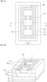
- FIG. 4A is a plan view of a power semiconductor device 100 according to embodiments
- FIG. 4B is a partial three-dimensional cross-sectional view of the power semiconductor device 100 according to the example shown in FIG. 4A along the line A-A'.
- the power semiconductor device 100 can include one or more of a substrate 110, a first conductivity type epitaxial layer 120, a stepped second conductive well 130, a buried insulating layer 150, a first conductivity type source region 140, a gate insulating layer 160, a junction electric field region 122, a second conductivity type ion implantation region 135 (see FIG. 4B ), a gate 170, a interlayer insulating layer 180, and/or a source electrode 190.
- the stepped second conductivity type well 130 can include a second conductivity type second-first well 131 and a second conductivity type second-second well 132.
- the first conductivity type can be N-type
- the second conductivity type can be P-type, but is not limited thereto.
- the substrate 110 and the first conductivity type epitaxial layer 120 can include silicon carbide (SiC), but is not limited thereto.
- the power semiconductor device 100 can include a substrate 110, a first conductivity type epitaxial layer 120 disposed on the substrate 110, a stepped second conductivity type well 130 disposed on the first conductivity type epitaxial layer 120 and a source region 140 disposed to be partially spaced apart from a first region of the stepped second conductivity type well 130 and spaced apart from each other, a buried insulating layer 150 disposed in a second region of the second conductivity type well 130 between the source regions 140 and a second conductivity type ion implantation region 135 disposed on one side of the stepped second conductivity type well 130.
- the power semiconductor device 100 can include a gate insulating layer 160 disposed on the stepped second conductivity type well 130 and a gate 170 disposed on the gate insulating layer 160. and an interlayer insulating layer 180 disposed on the gate 170 and a source electrode 190 disposed on the source region 140.
- SiC Silicon Carbide
- ion implantation must be performed with an energy of at least about 650 KeV.
- the second conductivity type second-first well 131 can be formed, and a part of the second conductivity type second-first well 131 can be removed to form a trench structure.
- the second conductivity type second-second well 132 can be formed by using the ion implantation with the trench structure such that the stepped second conductivity type well 130 can be formed. Therefore, the power semiconductor device according to the embodiment can enhance the SCWT characteristics by the stepped second conductivity type well 130.
- the stepped second conductivity type well 130 can include the second conductivity type second-first well 131 having a first width W1 and a second conductivity type second-second well 132 having a third width W3 narrower than the first width W1 and disposed under the second conductivity type second-first well 131.
- the buried insulating layer 150 can be disposed in a region of the second conductivity type well 130 between the source regions 140 and can have a second width W2 less than the third width W3 of the second conductivity type second-second well 132.
- the stepped type second conductivity type well 130 can include the second conductivity type second-first well 131 having a first width W1 and the second conductivity type second-second well 132 having a third width W3 less than the first width W1 and disposed below the second conductivity type second-first well, there is a technical effect that can enhance the SCWT characteristics.
- the SCWT of VDMOSFET was about 2.4 ⁇ s level, and when this invention according to the embodiment was applied, the SCWT has be significantly improved to about 6.8 ⁇ s level.
- the JFET region can be designed to be further spaced apart in a depth direction of the substrate. So, there is a special technical effect that can improve a loss of the Ron characteristic by preventing the increase of the R JFET by maintaining a high withstand voltage characteristic.
- a spacing between a pair of second conductivity type second-second wells 132 (about twice the size of JW2) can be controlled be wider than the spacing between a pair of second conductivity type second-first wells 131(about twice that of JW1). So, there is a special technical effect that can improve the Ron characteristics by preventing the increase of R JFET .
- FIG. 4A is a plan view of the power semiconductor device 100 according to embodiments
- FIG. 4B is a partial three-dimensional cross-sectional view taken along line A-A' of the power semiconductor device 100 according to the example shown in FIG. 4A (the buried insulating layer 150 is omitted).
- the power semiconductor device 100 can include a substrate 110, a first conductivity type epitaxial layer 120 disposed on the substrate 110, and a stepped second conductivity type well 130 disposed on the epitaxial layer 120, the source region 140 disposed to be partially spaced apart and at a first region of the stepped second conductivity type well 130, a buried insulating layer 150 disposed in the second conductivity type well 130 between the spaced apart source regions 140 and a second conductivity type ion implantation region 135 disposed on one side of the stepped second conductivity type well 130.
- the power semiconductor device 100 can include a source electrode 190 disposed on the source region 140 and the second conductivity type ion implantation region 135.
- the horizontal width Ws of the contact region 190C of the source electrode can be greater than the horizontal width of the second conductivity type ion implantation region 135, and can be in contact with the source region 140 and the second conductivity type ion implantation region 135.
- the width of the second conductivity type second-second well 132 disposed on the lower side can be controlled to be smaller than the width of the second conductivity type second-first well 131 disposed on the upper side.
- the stepped second conductivity type well 130 including the second conductivity type second-first well 131 and the second conductivity type second-second well 132 arranged in a narrow width can be deeply formed.
- the embodiment has a special technical effect capable of providing a power semiconductor device, a power semiconductor module, and a power converter which is capable of increasing the robustness by enhancing the short circuit withstand time (SCWT) properties.
- SCWT short circuit withstand time
- a substrate 110 including a first conductivity type epitaxial layer 120 can be prepared, and a second conductivity type second-first well 131 can be formed on the first conductivity type epitaxial layer 120.
- the substrate 110 and the first conductivity type epitaxial layer 120 can include a 4H-SiC material, but are not limited thereto.
- the substrate 110 and the first conductivity type epitaxial layer 120 can include 3C-SiC or 6H-SiC.
- the first conductivity type epitaxial layer 120 can be an N-type drift region, but is not limited thereto.
- the second conductivity type second-first well 131 can be ion-implanted with a P-type dopant at a concentration of about 1 ⁇ 10 16 cm -3 to about 1 ⁇ 10 19 cm -3 .
- a P-type dopant at a concentration of about 1 ⁇ 10 16 cm -3 to about 1 ⁇ 10 19 cm -3 .
- Al or boron can be implanted, but is not limited thereto.
- a first conductivity type source region 140 can be formed in the second conductivity type second-first well 131.
- the first conductivity type source region 140 can be formed by ion-implanting an N-type dopant such as nitrogen or phosphorus at a concentration of about 1 ⁇ 10 17 cm -3 to about 2 ⁇ 10 20 cm -3 .
- a second conductivity type ion implantation region 135 can be formed.
- Al or boron can be implanted into the second conductivity type second-first well 131 at a deeper location through the first conductivity type source region 140 to form the second conductivity type ion implantation region 135.
- a junction electric field regions 122 can be formed on both sides of the second conductivity type ion implantation region 135.
- the junction field region 122 can be referred to as a JFET region.
- the junction electric field region 122 can be formed through ion implantation of a P-type dopant such as phosphorus, and characteristics of Vth, saturation current, and on-resistance can be improved.
- a trench T can be formed in the second conductivity type second-first well 131.
- a trench T can be formed to remove portions of the source region 140, the second conductivity type ion implantation region 135, and the second conductivity type second-first well 131 by etching.
- the first conductivity type epitaxial layer 120 cannot be exposed by the trench T.
- the second conductivity type second-second well 132 can be formed on a bottom and sidewalls of the trench T through an ion implantation process to form a step difference such that the type second conductivity type well 130 can be manufactured.
- the stepped second conductivity type Well 130 can be formed.
- the second conductivity type second-second well 132 can be formed through an activation process after performing ion implantation four times with tilt and rotation of 90° on each four side surfaces respectively and one ion implantation on the bottom surface.
- the width of the second conductivity type second-second well 132 is controlled to be smaller than that of the second conductivity type second-first well 131, there is a special technical effect that can improve the loss of Ron characteristics by preventing an increase of R JFET by maintaining high withstand voltage characteristics by controlling JFET region to be further spaced apart in the depth direction of the substrate.
- a buried insulating layer 150 can be formed in the second conductive type well 130 between the source regions 140 separated by the trench.
- the buried insulating layer 150 can be formed of oxide or nitride.
- a gate insulating layer 160 can be formed on the stepped second conductivity type well 130, a gate 170 can be formed on the gate insulating layer 160. And an interlayer insulating layer 180 can be formed on the gate 170, and a source electrode 190 can be formed on the source region 140 after partially opening the interlayer insulating layer 180.
- the gate insulating layer 160 can be a thermal oxide layer or a deposition oxide layer, but is not limited thereto.
- the gate 170 can be formed of polysilicon, but is not limited thereto.
- the interlayer insulating layer 180 can be formed of an oxide film or a nitride film, but is not limited thereto.
- the source electrode 190 can be formed of Al or the like, but is not limited thereto.
- the power semiconductor device the power semiconductor module, and the power converter including the same of the embodiment, there are technical effects of improving SCWT characteristics while minimizing Ron increase by the stepped second conductivity type well 130 designed to be deeply located.
- MOSFET devices for power semiconductors with a high-power switching function can have a higher robustness as SCWT (Short Circuit Withstand Time) increases as explained above.
- SCWT Short Circuit Withstand Time
- SiC VDMOSFET for example
- a shallow P-well structure for ease manufacturing within the line where withstand voltage can be secured may see the robustness of the power semiconductor device weakened due to a shortening of the SCWT.
- One of the technical objects of embodiments described herein is to provide a power semiconductor device and a power converter including the same that addresses this issue.
- One approach to solving the issue is by a stepped second conductivity type well designed to be deeply located.
- a stepped second conductivity type well 130 can include a second conductivity type second-first well 131 disposed on an upper side and a second conductivity type second-second well 132 disposed on a lower side.
- a width of the second conductivity type second-second well 132 disposed on the lower side can be controlled to be smaller than that of the second conductivity type second-first well 131 disposed on the upper side.
- the JFET region can be designed to be further spaced apart in a depth direction of the substrate. Therefore, there is a special technical effect that can improve a loss of the Ron characteristic by preventing the increase of the R JFET by maintaining a high withstand voltage characteristic.
- a power semiconductor device can include a substrate, a first conductivity type epitaxial layer disposed on the substrate, a stepped second conductivity type well disposed on the first conductivity type epitaxial layer, a source region partially spaced apart from a first region of the stepped second conductivity type well, a buried insulating layer disposed in a second region of the second conductive type well between the spaced apart source regions, a gate insulating layer disposed on the stepped second conductivity type well, a gate disposed on the gate insulating layer, an interlayer insulating layer disposed on the gate and a source electrode disposed on the source region.
- the stepped second conductivity type well can include a second conductivity type second-first well having a first width, and a second conductivity type second-second well having a third width narrower than the first width and disposed under the second conductivity type second-first well.
- the buried insulating layer can be disposed in a region of the second conductivity type well between the spaced apart source regions.
- a horizontal width of the buried insulating layer can be a second width smaller than the third width of the second conductivity type second-second well.
- a doping concentration of the second conductivity type second-second well can be equal or less than that of the second conductivity type second-first well.
- the power semiconductor device can include a second conductivity type ion implantation region disposed on one side of the stepped second conductivity type well.
- a horizontal width of a contact region of the source electrode can be greater than that of the second conductivity type ion implantation region.
- the contact area of the source electrode can be contact with the source region and the second conductivity type ion implantation region.
- a power converter according to the embodiment can include at least one of the power semiconductor devices as above.
- the stepped second conductivity type well 130 can include the second conductivity type second-first well 131 and the second conductivity type second-second well 132 disposed there below with a narrow width, there is a special technical effect that can enhance the SCWT characteristics by designing the second conductivity type second-second well 132 to be deeply located.
Landscapes
- Electrodes Of Semiconductors (AREA)
- Metal-Oxide And Bipolar Metal-Oxide Semiconductor Integrated Circuits (AREA)
Abstract
A power semiconductor device, a power semiconductor module including the same, a power converter, and methods of manufacture are provided. The power semiconductor device can include a substrate, a first conductivity type epitaxial layer disposed on the substrate, and a stepped well structure, where the width of a lower region of the stepped well structure is narrower than an upper region, but wider than an insulating or trench region.
Description
- The embodiments relate to semiconductor devices and manufacture, and in particular, to a power semiconductor module and a power converter including the same.
- Power semiconductors are one of the key factors that determine the efficiency, speed, durability and reliability of power electronic systems.
- With the recent development of the power electronics industry, as the previously used silicon (Si) power semiconductors reach their physical limits, research on WBG (Wide Bandgap) power semiconductors such as silicon carbide (SiC) and gallium nitride (GaN) to replace Si power semiconductors is being actively conducted.
- WBG power semiconductor devices have bandgap energy about 3 times that of Si power semiconductor devices, resulting in low intrinsic carrier concentration, high dielectric breakdown field (about 4 to 20 times), and high thermal conductivity (about 3 to 13 times) and a large electron saturation rate (about 2 to 2.5 times).
- Due to these characteristics, it can operate in a high-temperature, high-voltage environment and has high switching speed and low switching loss. Among them, a gallium nitride (GaN) power semiconductor device can be used for a low voltage system, and a silicon carbide (SiC) power semiconductor device can be used for a high voltage system.
- A SiC MOSFET of power semiconductor device may be denoted as VDMOSFET (Vertical Diffused MOSFET) with a vertical diffused structure, or may be simply denoted as DMOSFET (Double Diffused MOSFET) with a double-diffused structure. Also, SiC MOSFET can be classified into a Planar MOSFET and a Trench MOSFET according to the channel direction.
- However, there remains a need for improved power semiconductor devices, circuits or other modules incorporating power semiconductor devices, and methods of manufacture for power semiconductor devices.
- For instance, the SiC VDMOSFET of the related art includes a shallow P-well structure for ease of fabrication in the line where withstand voltage can be secured. This shallow P-well structure has an effect of reducing RJFET compared to Deep P-well structure. JFET refers to a pair of P-well region gaps located below the gate electrode. On the other hand, in the MOSFET device for power semiconductors having a high-power switching function, a robustness of the MOSFET device increases as a short circuit withstand time (SCWT) of the MOSFET device increases. The SCWT refers to a time that the MOSFET device can operate reliably when exposed to a short-circuit current.
- However, conventional SiC VDMOSFET shows superiority in electrical characteristics compared to Si MOSFET due to high breakdown voltage and low Ron characteristics, but the SCWT of the conventional SiC VDMOSFET is relatively short so a robustness of the conventional SiC VDMOSFET is weak.
- Embodiments described herein may address one or more of these challenges. According to some embodiments, a power semiconductor device, a power semiconductor module including the same, and a power converter that solve the problem that the SCWT is short are provided.
- The object is solved by the features of the independent claims. Preferred embodiments are given in the dependent claims.
- A power semiconductor device according to the embodiments may have a substrate and a stepped well.
- The stepped well may have a first region, a second region, and an insulating layer in the first region.
- The first region may have a width W1, the second region may have a width W3, and the width W1 may be greater than the width W3.
- The second region may be located below the first region.
- The insulating layer may be a buried insulating layer having a width W2, and the width W3 may be greater than the width W2.
- Further, the embodiments may have a source region.
- The source region may have a first portion and a second portion.
- The first and second portions of the source region may be separated by the insulating layer.
- At least the second region of the stepped well may be formed in a first conductivity type epitaxial layer on the substrate.
- Both the first and second regions of the stepped well may have a second conductivity type and the source region may have the first conductivity type.
- At least one of the substrate or the epitaxial layer may have silicon carbide (SiC).
- A doping concentration of the second region of the stepped well may be less than or equal to the doping concentration of the first region of the stepped well.
- Further, the embodiments may have a gate insulating layer disposed on the stepped well, a gate disposed on the gate insulating layer, an interlayer insulating layer disposed on the gate and a source electrode disposed on a source region of the device.
- Further, the embodiments may have an ion implantation region disposed on at least one side of the stepped well.
- A width of a contact region of the source electrode may be greater than a width of the ion implantation region.
- A contact area of the source electrode may be in contact with the source region and the ion implantation region.
- Further, the embodiments may have a plurality of stepped wells.
- A first of the plurality of stepped wells may be separated from a second of the plurality of stepped wells by an ion implantation region.
- A power converter according to the embodiments may have at least one power semiconductor device as described above.
- A method for manufacturing a semiconductor device according to the embodiments may have the step of forming, on a substrate, a first epitaxial layer and a first well, wherein the first epitaxial layer has a first conductivity type and the first well has a second conductivity type, forming a source region in the first well, wherein the source region has the first conductivity type; forming an ion implantation region) in the first well and through the source region, wherein the ion implantation region has the second conductivity type and extends deeper into the first well than the source region, forming one or more junction field effect (JFET) regions on either side of the ion implantation region, forming a trench in the first well and forming a stepped-well structure comprising the first well and a second well below the first well.
- Further, the embodiments may have a step of applying an insulating layer in the trench.
- The forming the stepped-well structure may have a step of performing an ion implantation on a bottom of the trench to generate the second well.
- The forming the stepped-well structure may have a step of performing a plurality of ion implementation steps and performing an activation process.
- The performing a plurality of ion implementation steps may have a step of performing ion implantation with tilt and rotation of 90° on each of four side surfaces of the trench, respectively, and at least one ion implantation on the bottom surface.
- A second conductivity type dopant concentration in the second well may be equal or less than that in the first well.
- A width of the second well may be smaller than a width of the first well in the stepped-well structure.
- The forming the trench may create a first portion of the source region and a second portion of the source region, the insulating layer may be applied between the first and second portions, and the first epitaxial layer in a region below the first well may not be exposed by formation of the trench.
- According to the power semiconductor device, a power semiconductor module, and a power converter including the same of the embodiment, there are technical effects of improving SCWT characteristics while minimizing Ron increase by a stepped second conductivity type well designed to be deeply located.
- For example, according to the embodiment, a stepped second conductivity type well can include a second conductivity type second-first well disposed on an upper side and a second conductivity type second-second well disposed on a lower side. In this case, a width of the second conductivity type second-second well disposed on the lower side can be controlled to be smaller than that of the second conductivity type second-first well disposed on the upper side. Accordingly, the JFET region can be designed to be further spaced apart in a depth direction of the substrate. Therefore, there is a special technical effect that can improve a loss of the Ron characteristic by preventing the increase of the RJFET by maintaining a high withstand voltage characteristic.
- Further, according to the embodiment, a physical distance between the channel and a bottom surface of the second conductive type well can be increased by the stepped second conductivity type well including deeply located second conductivity type second-second well such that concentration of the electric field in a channel can be reduced. So, there is a technical effect of reducing a channel resistance by improving a short channel effect.
- In addition, according to the embodiment, the stepped second conductivity type well can include the second conductivity type second-first well and the second conductivity type second-second well disposed there below with a narrow width, there is a special technical effect that can enhance the SCWT characteristics by designing the second conductivity type second-second well to be deeply located.
- Through this, the embodiment has a special technical effect capable of providing a power semiconductor device, a power semiconductor module including the same, and a power converter capable of increasing the robustness by enhancing the SCWT characteristics.
- The technical effects of the embodiments are not limited to those described in this section, but include those that can be understood through the description of the invention.
- The accompanying drawings, which are incorporated herein and form part of the specification, illustrate various, non-limiting embodiments of the present invention. In the drawings, like reference numbers indicate identical or functionally similar elements.
-
FIG. 1 illustrates a power converter according to embodiments. -
FIG. 2 illustrates a cross-sectional view of a power semiconductor device of embodiments. -
FIG. 3A, 3B illustrate cross-sectional views of a power semiconductor device of embodiments. -
FIG. 4A illustrates a plan view of a power semiconductor device according to embodiments. -
FIG. 4B illustrates a partial cross-sectional view of a power semiconductor device of embodiments. -
FIGS. 5A to 5I illustrate cross-sectional views of a manufacturing process of a power semiconductor device according to embodiments. - Hereinafter, embodiments are described in detail with reference to the drawings.
- The suffixes "module" and "unit" for the elements used in the following description are simply given in consideration of ease of writing this specification, and do not themselves give a particularly important meaning or role. Accordingly, the "module" and "unit" can be used interchangeably.
- Terms including ordinal numbers, such as first and second, can be used to describe various elements, but the elements are not limited by the terms. These terms are only used for the purpose of distinguishing one element from another.
- Singular expressions include plural expressions unless the context clearly dictates otherwise.
- In this application, terms such as "comprise", "have" or "include" are intended to designate that there is a feature, number, step, operation, component, part, or combination thereof described in the specification, and it is not precluded from being excluded one or other features, numbers, steps, operations, components, parts, or combinations thereof, or any combination thereof.
- Referring now to
FIG. 1 , apower converter 1000 is provided according to one or more embodiments. - The
power converter 1000 according to the embodiment can receive DC power from a battery or fuel cell, convert it into AC power, and supply AC power to a predetermined load. For example, thepower converter 1000 according to the embodiment can include an inverter, which receives DC power from a battery, converts DC power into 3-phase AC power, and supplies 3-phase AC power to a motor M. In certain aspects, motor M can provide power to electric vehicles or fuel cell vehicles. - Referring now to
FIG. 1 , apower converter 1000 is provided according to one or more embodiments. - The
power converter 1000 according to embodiments can include one or morepower semiconductor devices 100. Thepower semiconductor device 100 can be, for example, a Metal Oxide Semiconductor Field Effect Transistor (MOSFET), but is not limited thereto. For instance, it could be an Insulated Gate Bipolar Transistor (IGBT) in some embodiments. According to embodiments, MOSFETs, such as SiC MOSFETS, can have various structures. Examples include a trench structure MOSFET, a vertical doubly implanted structure MOSFET (DIMOSFETs), or a lateral diffused structure MOSFET, etc. - In some embodiments, the
power converter 1000 can include a plurality ofpower semiconductor devices power converter 1000 may also have a plurality of diodes (not shown). In certain aspects, each of the plurality of diodes can be internally incorporated in each of thepower semiconductor devices - In the example of
FIG. 1 , DC power can be converted into AC power through on-off control of the plurality ofpower semiconductor devices 100a to 100f. For instance, in thepower converter 1000 according to embodiments, the firstpower semiconductor device 100a can be turned on and the secondpower semiconductor device 100b can be turned off in a first time period of one cycle to supply positive polarity power to the motor M. In addition, in the second time period of one cycle, the firstpower semiconductor device 100a can be turned off and the secondpower semiconductor device 100b can be turned on to supply negative polarity power to the motor M. - A group of power semiconductor devices disposed in series in a high voltage line and a low voltage line of an input side can be referred to as an arm. For example, the first
power semiconductor device 100a and the secondpower semiconductor device 100b can constitute a first arm, and the thirdpower semiconductor device 100c and the fourthpower semiconductor device 100d can constitute a second arm. And the fifthpower semiconductor device 100e and the sixthpower semiconductor device 100f can constitute a third arm. - In the arm, an upper side power semiconductor device and a lower side power semiconductor device can be controlled not to turn on at the same time. For example, in the first arm, the first
power semiconductor device 100a and the secondpower semiconductor device 100b do not simultaneously turn on, but can turn on and off alternately. - In some embodiments, each of the
power semiconductor devices 100a to 100f can receive high power in an off state. For example, when the secondpower semiconductor device 100b is turned off while the firstpower semiconductor device 100a is turned on, the input voltage can be applied to the secondpower semiconductor device 100b as it is. The voltage input to the secondpower semiconductor device 100b can be a relatively high voltage, and a withstand voltage of eachpower semiconductor device 100a to 100f can be designed to have a high level to withstand such a high voltage. - Additionally, and in certain aspects, each of the
power semiconductor devices 100a to 100f can conduct a high current in a turn on state. The motor M can be driven with a relatively high current, and this high current can be supplied to the motor M through a power semiconductor that is turned on. - A high voltage applied to each of the
power semiconductor devices 100a to 100f can cause a high switching loss. A high current conducting thepower semiconductor devices 100a to 100f can cause a high conduction loss. In order to dissipate heat generated by such switching loss or conduction loss, thepower semiconductor devices 100a to 100f can be packaged as a power semiconductor module including a heat dissipation means. - In some embodiments, the
power semiconductor device 100 can be a silicon carbide (SiC) power semiconductor device. In certain aspects, it can operate in a high-temperature, high-voltage environment, and can have a high switching speed and low switching loss. - In some embodiments, the
power converter 1000 according to the embodiment can include a plurality of power semiconductor modules. - For example, the plurality of
power semiconductor devices 100a to 100f shown inFIG. 1 can be packaged into one power semiconductor module, or the power semiconductor devices constituting each arm can be packaged into one power semiconductor module. - As another example, the first
power semiconductor device 100a, the secondpower semiconductor device 100b, the thirdpower semiconductor device 100c, the fourthpower semiconductor device 100d, and the fifthpower semiconductor device 100e and the sixthpower semiconductor device 100f shown inFIG. 1 can be packaged into one power semiconductor module. - In addition, there can be additional power semiconductor devices disposed in parallel with each of the
power semiconductor devices 100a to 100f to increase a current capacity. In this case, the number of power semiconductor devices included in the power semiconductor module can be greater than six. - The
power converter 1000 according to embodiments can include a diode-type power semiconductor device in addition to the transistor-typepower semiconductor devices 100a to 100f. For example, a first diode (not shown) can be disposed in parallel with the firstpower semiconductor device 100a, and a second diode (not shown) can be disposed in parallel with the secondpower semiconductor device 100b. Also, these diodes can be packaged together in one power semiconductor module. In addition, the diode can be disposed in the form of an internal diode in each power semiconductor device. - In some embodiments, the power semiconductor devices constituting each arm can be packaged into one power semiconductor module. For example, the first
power semiconductor device 100a and the secondpower semiconductor device 100b constituting the first arm can be packaged as a first power semiconductor module. The thirdpower semiconductor device 100c and the fourthpower semiconductor device 100d constituting the second arm can be packaged into a second power semiconductor module. And the fifthpower semiconductor device 100e and the sixthpower semiconductor device 100f constituting the third arm can be packaged into a third power semiconductor module. - In addition, there can be additional power semiconductor devices arranged in parallel with each
power semiconductor device 100a to 100f to increase a current capacity. In this case, the number of power semiconductor devices included in each power semiconductor module can be more than two. Also, each arm can include a diode-type power semiconductor device (not shown) in addition to the transistor-typepower semiconductor devices 100a to 100f, and these diodes can also be packaged together in one power semiconductor module. In addition, the diode can be disposed in a form of an internal diode in each power semiconductor device. -
FIG. 2 illustrates a cross-sectional view of a power semiconductor device, such asdevice 100, according to embodiments. In certain aspects, this device may be used in a circuit or other module, such as apower converter 1000 as described in connection withFIG. 1 . - The
power semiconductor device 100, such as a MOSFET, according to embodiments can include asource electrode 190 disposed above asemiconductor epitaxial layer 120, agate electrode 175, and adrain electrode 105 disposed below thesemiconductor epitaxial layer 120. - In embodiments, the
source electrode 190 or thegate electrode 175 can include an Al-based metal, and thedrain electrode 105 can include Ti/Ni/Ag metal including a Ti layer, a Ni layer, or an Ag layer, or NiV/Ag, V(vanadium)/Ni/Ag, or the like, but is not limited thereto. -
FIG. 3A is a cross-sectional view of apower semiconductor device 100 according to embodiments, andFIG. 3B is a detailed cross-sectional view of thepower semiconductor device 100 according to the example shown inFIG. 3A . -
FIG. 4A is a plan view of apower semiconductor device 100 according to embodiments, andFIG. 4B is a partial three-dimensional cross-sectional view of thepower semiconductor device 100 according to the example shown inFIG. 4A along the line A-A'. - Referring to
FIG. 3A , thepower semiconductor device 100 according to the embodiment can include one or more of asubstrate 110, a first conductivitytype epitaxial layer 120, a stepped second conductive well 130, a buried insulatinglayer 150, a first conductivitytype source region 140, agate insulating layer 160, a junctionelectric field region 122, a second conductivity type ion implantation region 135 (seeFIG. 4B ), agate 170, ainterlayer insulating layer 180, and/or asource electrode 190. - According to embodiments, the stepped second conductivity type well 130 can include a second conductivity type second-
first well 131 and a second conductivity type second-second well 132. The first conductivity type can be N-type, and the second conductivity type can be P-type, but is not limited thereto. Further, thesubstrate 110 and the first conductivitytype epitaxial layer 120 can include silicon carbide (SiC), but is not limited thereto. - Specifically, referring to
FIG. 3A , thepower semiconductor device 100 according to the embodiment can include asubstrate 110, a first conductivitytype epitaxial layer 120 disposed on thesubstrate 110, a stepped second conductivity type well 130 disposed on the first conductivitytype epitaxial layer 120 and asource region 140 disposed to be partially spaced apart from a first region of the stepped second conductivity type well 130 and spaced apart from each other, a buried insulatinglayer 150 disposed in a second region of the second conductivity type well 130 between thesource regions 140 and a second conductivity typeion implantation region 135 disposed on one side of the stepped second conductivity type well 130. - In addition, the
power semiconductor device 100 according to embodiments can include agate insulating layer 160 disposed on the stepped second conductivity type well 130 and agate 170 disposed on thegate insulating layer 160. and an interlayer insulatinglayer 180 disposed on thegate 170 and asource electrode 190 disposed on thesource region 140. - It may be difficult to ion implant into SiC (Silicon Carbide), which may be employed in some embodiments, due to the nature of the material. For example, in order to form a p-well of about 1 µm, ion implantation must be performed with an energy of at least about 650 KeV. Thus, there are technical difficulties in a mass production process for forming wells having a deep depth of 2 µm to 3 µm by ion implantation.
- However, one or more of the embodiments described herein can provide power semiconductor devices that address these technical difficulties. According to some embodiments, the second conductivity type second-
first well 131 can be formed, and a part of the second conductivity type second-first well 131 can be removed to form a trench structure. - Additionally, the second conductivity type second-second well 132 can be formed by using the ion implantation with the trench structure such that the stepped second conductivity type well 130 can be formed. Therefore, the power semiconductor device according to the embodiment can enhance the SCWT characteristics by the stepped second conductivity type well 130.
- Referring to
FIG. 3B , the stepped second conductivity type well 130 can include the second conductivity type second-first well 131 having a first width W1 and a second conductivity type second-second well 132 having a third width W3 narrower than the first width W1 and disposed under the second conductivity type second-first well 131. - Also, the buried insulating
layer 150 can be disposed in a region of the second conductivity type well 130 between thesource regions 140 and can have a second width W2 less than the third width W3 of the second conductivity type second-second well 132. - Therefore, according to the embodiment, since the stepped type second conductivity type well 130 can include the second conductivity type second-
first well 131 having a first width W1 and the second conductivity type second-second well 132 having a third width W3 less than the first width W1 and disposed below the second conductivity type second-first well, there is a technical effect that can enhance the SCWT characteristics. In the internal technology, the SCWT of VDMOSFET was about 2.4 µs level, and when this invention according to the embodiment was applied, the SCWT has be significantly improved to about 6.8 µs level. - In particular, since the third width of the second conductivity type second-second well 132 disposed on the lower side can be controlled to be less than that of the second conductivity type second-
first well 131 disposed on the upper side, the JFET region can be designed to be further spaced apart in a depth direction of the substrate. So, there is a special technical effect that can improve a loss of the Ron characteristic by preventing the increase of the RJFET by maintaining a high withstand voltage characteristic. - For example, a spacing between a pair of second conductivity type second-second wells 132 (about twice the size of JW2) can be controlled be wider than the spacing between a pair of second conductivity type second-first wells 131(about twice that of JW1). So, there is a special technical effect that can improve the Ron characteristics by preventing the increase of RJFET.
- Next,
FIG. 4A is a plan view of thepower semiconductor device 100 according to embodiments, andFIG. 4B is a partial three-dimensional cross-sectional view taken along line A-A' of thepower semiconductor device 100 according to the example shown inFIG. 4A (the buried insulatinglayer 150 is omitted). - Referring to
FIGS. 4A and 4B , thepower semiconductor device 100 according to the embodiment can include asubstrate 110, a first conductivitytype epitaxial layer 120 disposed on thesubstrate 110, and a stepped second conductivity type well 130 disposed on theepitaxial layer 120, thesource region 140 disposed to be partially spaced apart and at a first region of the stepped second conductivity type well 130, a buried insulatinglayer 150 disposed in the second conductivity type well 130 between the spaced apartsource regions 140 and a second conductivity typeion implantation region 135 disposed on one side of the stepped second conductivity type well 130. - Referring to
FIG. 4B , thepower semiconductor device 100 according to the embodiment can include asource electrode 190 disposed on thesource region 140 and the second conductivity typeion implantation region 135. The horizontal width Ws of thecontact region 190C of the source electrode can be greater than the horizontal width of the second conductivity typeion implantation region 135, and can be in contact with thesource region 140 and the second conductivity typeion implantation region 135. - Referring to
FIG. 4B , in an embodiment, the width of the second conductivity type second-second well 132 disposed on the lower side can be controlled to be smaller than the width of the second conductivity type second-first well 131 disposed on the upper side. By designing the JFET area to be further spaced apart in the depth direction of the substrate, there is a special technical effect that can improve the loss of Ron characteristics by maintaining high withstand voltage characteristics and preventing the increase of RJFET. - In addition, according to the embodiment, the stepped second conductivity type well 130 including the second conductivity type second-
first well 131 and the second conductivity type second-second well 132 arranged in a narrow width can be deeply formed. - There is a special technical effect that can enhance the SCWT characteristics by controlling second conductivity type second-second well 132 be deeply located. Through this, the embodiment has a special technical effect capable of providing a power semiconductor device, a power semiconductor module, and a power converter which is capable of increasing the robustness by enhancing the short circuit withstand time (SCWT) properties.
- Next, a manufacturing process of a
power semiconductor device 100 according to embodiments will be described with reference toFIGS. 5A to 5I . - Referring to
FIG. 5A , asubstrate 110 including a first conductivitytype epitaxial layer 120 can be prepared, and a second conductivity type second-first well 131 can be formed on the first conductivitytype epitaxial layer 120. - The
substrate 110 and the first conductivitytype epitaxial layer 120 can include a 4H-SiC material, but are not limited thereto. For example, thesubstrate 110 and the first conductivitytype epitaxial layer 120 can include 3C-SiC or 6H-SiC. The first conductivitytype epitaxial layer 120 can be an N-type drift region, but is not limited thereto. - The second conductivity type second-
first well 131 can be ion-implanted with a P-type dopant at a concentration of about 1×1016 cm-3 to about 1×1019 cm-3. For example, Al or boron can be implanted, but is not limited thereto. - Next, referring to
FIG. 5B , a first conductivitytype source region 140 can be formed in the second conductivity type second-first well 131. For example, the first conductivitytype source region 140 can be formed by ion-implanting an N-type dopant such as nitrogen or phosphorus at a concentration of about 1×1017 cm-3 to about 2×1020 cm-3. - Next, referring to
FIG. 5C , a second conductivity typeion implantation region 135 can be formed. For example, Al or boron can be implanted into the second conductivity type second-first well 131 at a deeper location through the first conductivitytype source region 140 to form the second conductivity typeion implantation region 135. - Next, referring to
FIG. 5D , a junctionelectric field regions 122 can be formed on both sides of the second conductivity typeion implantation region 135. Thejunction field region 122 can be referred to as a JFET region. The junctionelectric field region 122 can be formed through ion implantation of a P-type dopant such as phosphorus, and characteristics of Vth, saturation current, and on-resistance can be improved. - Referring to
FIG. 5E , a trench T can be formed in the second conductivity type second-first well 131. For example, a trench T can be formed to remove portions of thesource region 140, the second conductivity typeion implantation region 135, and the second conductivity type second-first well 131 by etching. The first conductivitytype epitaxial layer 120 cannot be exposed by the trench T. - Next, referring to
FIGS. 5F and 5G (FIG. 5G is a three-dimensional cross-sectional view ofFIG. 5F ), the second conductivity type second-second well 132 can be formed on a bottom and sidewalls of the trench T through an ion implantation process to form a step difference such that the type second conductivity type well 130 can be manufactured. - For example, by forming the second conductivity type second-second well 132 through ion implantation on the sidewall and bottom of the trench T of the second conductivity type second-
first well 131, the stepped secondconductivity type Well 130 can be formed. For example, the second conductivity type second-second well 132 can be formed through an activation process after performing ion implantation four times with tilt and rotation of 90° on each four side surfaces respectively and one ion implantation on the bottom surface. - In addition, according to the embodiment, since the width of the second conductivity type second-
second well 132 is controlled to be smaller than that of the second conductivity type second-first well 131, there is a special technical effect that can improve the loss of Ron characteristics by preventing an increase of RJFET by maintaining high withstand voltage characteristics by controlling JFET region to be further spaced apart in the depth direction of the substrate. - Next, referring to
FIG. 5H , a buried insulatinglayer 150 can be formed in the second conductive type well 130 between thesource regions 140 separated by the trench. The buried insulatinglayer 150 can be formed of oxide or nitride. - Next, referring to
FIG. 5I , agate insulating layer 160 can be formed on the stepped second conductivity type well 130, agate 170 can be formed on thegate insulating layer 160. And an interlayer insulatinglayer 180 can be formed on thegate 170, and asource electrode 190 can be formed on thesource region 140 after partially opening theinterlayer insulating layer 180. - The
gate insulating layer 160 can be a thermal oxide layer or a deposition oxide layer, but is not limited thereto. Thegate 170 can be formed of polysilicon, but is not limited thereto. The interlayer insulatinglayer 180 can be formed of an oxide film or a nitride film, but is not limited thereto. The source electrode 190 can be formed of Al or the like, but is not limited thereto. - According to the power semiconductor device, the power semiconductor module, and the power converter including the same of the embodiment, there are technical effects of improving SCWT characteristics while minimizing Ron increase by the stepped second conductivity type well 130 designed to be deeply located.
- The design and manufacture of power semiconductor devices can introduce competing, and often contradictory, challenges for optimal performance.
- For instance, MOSFET devices for power semiconductors with a high-power switching function can have a higher robustness as SCWT (Short Circuit Withstand Time) increases as explained above.
- However, a SiC VDMOSFET (for example) that employs a shallow P-well structure for ease manufacturing within the line where withstand voltage can be secured may see the robustness of the power semiconductor device weakened due to a shortening of the SCWT.
- One of the technical objects of embodiments described herein is to provide a power semiconductor device and a power converter including the same that addresses this issue. One approach to solving the issue is by a stepped second conductivity type well designed to be deeply located.
- According to some embodiments, a stepped second conductivity type well 130 can include a second conductivity type second-
first well 131 disposed on an upper side and a second conductivity type second-second well 132 disposed on a lower side. In this case, a width of the second conductivity type second-second well 132 disposed on the lower side can be controlled to be smaller than that of the second conductivity type second-first well 131 disposed on the upper side. Accordingly, the JFET region can be designed to be further spaced apart in a depth direction of the substrate. Therefore, there is a special technical effect that can improve a loss of the Ron characteristic by preventing the increase of the RJFET by maintaining a high withstand voltage characteristic. - According to some embodiments, a power semiconductor device can include a substrate, a first conductivity type epitaxial layer disposed on the substrate, a stepped second conductivity type well disposed on the first conductivity type epitaxial layer, a source region partially spaced apart from a first region of the stepped second conductivity type well, a buried insulating layer disposed in a second region of the second conductive type well between the spaced apart source regions, a gate insulating layer disposed on the stepped second conductivity type well, a gate disposed on the gate insulating layer, an interlayer insulating layer disposed on the gate and a source electrode disposed on the source region.
- In certain aspects, the stepped second conductivity type well can include a second conductivity type second-first well having a first width, and a second conductivity type second-second well having a third width narrower than the first width and disposed under the second conductivity type second-first well.
- The buried insulating layer can be disposed in a region of the second conductivity type well between the spaced apart source regions.
- A horizontal width of the buried insulating layer can be a second width smaller than the third width of the second conductivity type second-second well.
- A doping concentration of the second conductivity type second-second well can be equal or less than that of the second conductivity type second-first well.
- Further, the power semiconductor device according to embodiments can include a second conductivity type ion implantation region disposed on one side of the stepped second conductivity type well.
- A horizontal width of a contact region of the source electrode can be greater than that of the second conductivity type ion implantation region.
- The contact area of the source electrode can be contact with the source region and the second conductivity type ion implantation region.
- A power converter according to the embodiment can include at least one of the power semiconductor devices as above.
- In addition, according to the embodiment, the stepped second conductivity type well 130 can include the second conductivity type second-
first well 131 and the second conductivity type second-second well 132 disposed there below with a narrow width, there is a special technical effect that can enhance the SCWT characteristics by designing the second conductivity type second-second well 132 to be deeply located. - While various aspects are described herein, it should be understood that they have been presented by way of example only, and not limitation. Thus, the breadth and scope of this disclosure should not be limited by any of the above-described exemplary aspects. Moreover, any combination of the above-described elements in all possible variations thereof is encompassed by the disclosure unless otherwise indicated herein or otherwise clearly contradicted by context.
- Additionally, while the processes described above as a sequence of steps, this was done solely for the sake of description. Accordingly, it is contemplated that some steps may be added, some steps may be omitted, the order of the steps may be re-arranged, and some steps may be performed in parallel.
Claims (15)
- A power semiconductor device (100), comprising:a substrate (110); anda stepped well (130), wherein the stepped well (130) comprises a first region, a second region, and an insulating layer (150) in the first region.
- The device of claim 1, wherein the first region has a width W1, the second region has a width W3, and the width W1 is greater than the width W3.
- The device of claim 2, wherein the second region is located below the first region.
- The device of claim 2 or 3, wherein the insulating layer (150) is a buried insulating layer having a width W2, and the width W3 is greater than the width W2.
- The device of any one of the preceding claims, further comprising a source region (140), wherein the source region (140) comprises a first portion and a second portion, and wherein the first and second portions of the source region (140) are separated by the insulating layer (150).
- The device of claim 5, wherein:(i) at least the second region of the stepped well (130) is formed in a first conductivity type epitaxial layer (120) on the substrate (110),(ii) both the first and second regions of the stepped well (130) have a second conductivity type, and(iii) the source region (140) has the first conductivity type.
- The device of claim 6, wherein at least one of the substrate (110) or the epitaxial layer (120) comprise silicon carbide (SiC).
- The device of any one of the preceding claims, wherein a doping concentration of the second region of the stepped well (130) is less than or equal to the doping concentration of the first region of the stepped well (130).
- The device of any one of the preceding claims, further comprising:a gate insulating layer (160) disposed on the stepped well (130);a gate (170) disposed on the gate insulating layer (160);an interlayer insulating layer (180) disposed on the gate (170); anda source electrode (190) disposed on a source region (140) of the device.
- The device of claim 9, further comprising:an ion implantation region (135) disposed on at least one side of the stepped well (130),wherein a width of a contact region of the source electrode (190) is greater than a width of the ion implantation region (135), andwherein a contact area of the source electrode (190) is in contact with the source region (140) and the ion implantation region (135).
- The device of any one of the preceding claims, comprising a plurality of stepped wells (130), wherein a first of the plurality of stepped wells (130) is separated from a second of the plurality of stepped wells (130) by an ion implantation region (135).
- A power converter (1000) comprising at least one power semiconductor device (100) according to any one of claims 1 to 11.
- A method for manufacturing a semiconductor device, comprising:forming, on a substrate (110), a first epitaxial layer (120) and a first well (131), wherein the first epitaxial layer (120) has a first conductivity type and the first well (131) has a second conductivity type;forming a source region (140) in the first well (131), wherein the source region (140) has the first conductivity type;forming an ion implantation region (135) in the first well (131) and through the source region (140), wherein the ion implantation region (135) has the second conductivity type and extends deeper into the first well (131) than the source region (140);forming one or more junction field effect (JFET) regions (122) on either side of the ion implantation region (135) ;forming a trench (T) in the first well (131); andforming a stepped-well structure comprising the first well (131) and a second well (132) below the first well (131).
- The method of claim 13, further comprising applying an insulating layer (150) in the trench (T).
- The method of claim 13, wherein forming the stepped-well structure comprises performing an ion implantation on a bottom of the trench (T) to generate the second well (132).
Applications Claiming Priority (1)
| Application Number | Priority Date | Filing Date | Title |
|---|---|---|---|
| KR1020230141832A KR20250058278A (en) | 2023-10-23 | 2023-10-23 | Power semiconductor device, power converter including the same and A method for manufacturing a semiconductor device |
Publications (1)
| Publication Number | Publication Date |
|---|---|
| EP4546974A1 true EP4546974A1 (en) | 2025-04-30 |
Family
ID=92672214
Family Applications (1)
| Application Number | Title | Priority Date | Filing Date |
|---|---|---|---|
| EP24198189.3A Pending EP4546974A1 (en) | 2023-10-23 | 2024-09-03 | Power semiconductor devices and methods |
Country Status (6)
| Country | Link |
|---|---|
| US (1) | US20250133768A1 (en) |
| EP (1) | EP4546974A1 (en) |
| JP (1) | JP2025071772A (en) |
| KR (1) | KR20250058278A (en) |
| CN (1) | CN119907281A (en) |
| TW (1) | TW202519032A (en) |
Citations (5)
| Publication number | Priority date | Publication date | Assignee | Title |
|---|---|---|---|---|
| US20030201483A1 (en) * | 2002-04-30 | 2003-10-30 | Nec Electronics Corporation | Vertical type MOSFET and manufacturing method thereof |
| US9070763B1 (en) * | 2014-03-26 | 2015-06-30 | Vanguard International Semiconductor Corporation | Semiconductor device layout structure |
| EP2966690A1 (en) * | 2008-03-26 | 2016-01-13 | Rohm Co., Ltd. | Semiconductor device, and method for manufacturing the same |
| US20220045213A1 (en) * | 2018-12-21 | 2022-02-10 | Abb Power Grids Switzerland Ag | Silicon Carbide Power Device with MOS Structure and Stressor |
| US20220069138A1 (en) * | 2020-08-27 | 2022-03-03 | Cree, Inc. | Power silicon carbide based semiconductor devices with improved short circuit capabilities and methods of making such devices |
-
2023
- 2023-10-23 KR KR1020230141832A patent/KR20250058278A/en active Pending
-
2024
- 2024-07-29 JP JP2024122312A patent/JP2025071772A/en active Pending
- 2024-08-14 US US18/804,562 patent/US20250133768A1/en active Pending
- 2024-09-03 EP EP24198189.3A patent/EP4546974A1/en active Pending
- 2024-09-04 TW TW113133544A patent/TW202519032A/en unknown
- 2024-09-23 CN CN202411324610.7A patent/CN119907281A/en active Pending
Patent Citations (5)
| Publication number | Priority date | Publication date | Assignee | Title |
|---|---|---|---|---|
| US20030201483A1 (en) * | 2002-04-30 | 2003-10-30 | Nec Electronics Corporation | Vertical type MOSFET and manufacturing method thereof |
| EP2966690A1 (en) * | 2008-03-26 | 2016-01-13 | Rohm Co., Ltd. | Semiconductor device, and method for manufacturing the same |
| US9070763B1 (en) * | 2014-03-26 | 2015-06-30 | Vanguard International Semiconductor Corporation | Semiconductor device layout structure |
| US20220045213A1 (en) * | 2018-12-21 | 2022-02-10 | Abb Power Grids Switzerland Ag | Silicon Carbide Power Device with MOS Structure and Stressor |
| US20220069138A1 (en) * | 2020-08-27 | 2022-03-03 | Cree, Inc. | Power silicon carbide based semiconductor devices with improved short circuit capabilities and methods of making such devices |
Also Published As
| Publication number | Publication date |
|---|---|
| TW202519032A (en) | 2025-05-01 |
| KR20250058278A (en) | 2025-04-30 |
| JP2025071772A (en) | 2025-05-08 |
| US20250133768A1 (en) | 2025-04-24 |
| CN119907281A (en) | 2025-04-29 |
Similar Documents
| Publication | Publication Date | Title |
|---|---|---|
| WO2018106326A1 (en) | Power semiconductor devices having gate trenches and buried termination structures and related methods | |
| KR20210019127A (en) | Power semiconductor devices having gate trenches with implanted sidewalls and related methods | |
| EP4521882A1 (en) | Power semiconductor device and power converter including the same | |
| US20250194145A1 (en) | Power semiconductor devices and power converter including the same | |
| EP4492470A1 (en) | Power semiconductor device, power semiconductor module, power converter including same, and manufacturing method thereof | |
| JP7841095B2 (en) | Semiconductor device, power converter, and method for manufacturing a semiconductor device | |
| US20250133768A1 (en) | Power semiconductor devices and methods | |
| EP4529386A1 (en) | A power semiconductor device and a power converter including the same | |
| EP4637294A1 (en) | Power semiconductor device and power converter including the same, and manufacturing method of power semiconductor device | |
| EP4572562A1 (en) | Power semiconductor device and power converter including the same | |
| US20250203926A1 (en) | Power semiconductor device and power converter including the same | |
| US20250203971A1 (en) | Power semiconductor device and power converter including the same | |
| KR20250109921A (en) | Power semiconductor devices and power conversion devices containing the same | |
| KR20250163252A (en) | Power semiconductor device and power converter including the same | |
| KR20250095466A (en) | Power semiconductor device and Power converter including the same |
Legal Events
| Date | Code | Title | Description |
|---|---|---|---|
| PUAI | Public reference made under article 153(3) epc to a published international application that has entered the european phase |
Free format text: ORIGINAL CODE: 0009012 |
|
| STAA | Information on the status of an ep patent application or granted ep patent |
Free format text: STATUS: THE APPLICATION HAS BEEN PUBLISHED |
|
| AK | Designated contracting states |
Kind code of ref document: A1 Designated state(s): AL AT BE BG CH CY CZ DE DK EE ES FI FR GB GR HR HU IE IS IT LI LT LU LV MC ME MK MT NL NO PL PT RO RS SE SI SK SM TR |
|
| STAA | Information on the status of an ep patent application or granted ep patent |
Free format text: STATUS: REQUEST FOR EXAMINATION WAS MADE |
|
| 17P | Request for examination filed |
Effective date: 20251014 |