EP4546657A1 - Multilevel coil array with inductive coupling for an electronic module - Google Patents
Multilevel coil array with inductive coupling for an electronic module Download PDFInfo
- Publication number
- EP4546657A1 EP4546657A1 EP24207787.3A EP24207787A EP4546657A1 EP 4546657 A1 EP4546657 A1 EP 4546657A1 EP 24207787 A EP24207787 A EP 24207787A EP 4546657 A1 EP4546657 A1 EP 4546657A1
- Authority
- EP
- European Patent Office
- Prior art keywords
- inductive coupling
- coil
- coils
- electronic module
- planar
- Prior art date
- Legal status (The legal status is an assumption and is not a legal conclusion. Google has not performed a legal analysis and makes no representation as to the accuracy of the status listed.)
- Pending
Links
Images


Classifications
-
- H—ELECTRICITY
- H04—ELECTRIC COMMUNICATION TECHNIQUE
- H04B—TRANSMISSION
- H04B5/00—Near-field transmission systems, e.g. inductive or capacitive transmission systems
- H04B5/20—Near-field transmission systems, e.g. inductive or capacitive transmission systems characterised by the transmission technique; characterised by the transmission medium
- H04B5/24—Inductive coupling
- H04B5/26—Inductive coupling using coils
- H04B5/263—Multiple coils at either side
-
- H—ELECTRICITY
- H04—ELECTRIC COMMUNICATION TECHNIQUE
- H04B—TRANSMISSION
- H04B5/00—Near-field transmission systems, e.g. inductive or capacitive transmission systems
- H04B5/20—Near-field transmission systems, e.g. inductive or capacitive transmission systems characterised by the transmission technique; characterised by the transmission medium
- H04B5/24—Inductive coupling
- H04B5/26—Inductive coupling using coils
-
- H—ELECTRICITY
- H01—ELECTRIC ELEMENTS
- H01F—MAGNETS; INDUCTANCES; TRANSFORMERS; SELECTION OF MATERIALS FOR THEIR MAGNETIC PROPERTIES
- H01F5/00—Coils
-
- H—ELECTRICITY
- H02—GENERATION; CONVERSION OR DISTRIBUTION OF ELECTRIC POWER
- H02J—ELECTRIC POWER NETWORKS; CIRCUIT ARRANGEMENTS OR SYSTEMS FOR SUPPLYING OR DISTRIBUTING ELECTRIC POWER; SYSTEMS FOR STORING ELECTRIC ENERGY
- H02J50/00—Circuit arrangements or systems for wireless supply or distribution of electric power
- H02J50/10—Circuit arrangements or systems for wireless supply or distribution of electric power using inductive coupling
-
- H—ELECTRICITY
- H02—GENERATION; CONVERSION OR DISTRIBUTION OF ELECTRIC POWER
- H02J—ELECTRIC POWER NETWORKS; CIRCUIT ARRANGEMENTS OR SYSTEMS FOR SUPPLYING OR DISTRIBUTING ELECTRIC POWER; SYSTEMS FOR STORING ELECTRIC ENERGY
- H02J50/00—Circuit arrangements or systems for wireless supply or distribution of electric power
- H02J50/20—Circuit arrangements or systems for wireless supply or distribution of electric power using microwaves or radio frequency waves
-
- H—ELECTRICITY
- H04—ELECTRIC COMMUNICATION TECHNIQUE
- H04B—TRANSMISSION
- H04B5/00—Near-field transmission systems, e.g. inductive or capacitive transmission systems
- H04B5/40—Near-field transmission systems, e.g. inductive or capacitive transmission systems characterised by components specially adapted for near-field transmission
- H04B5/43—Antennas
-
- H—ELECTRICITY
- H04—ELECTRIC COMMUNICATION TECHNIQUE
- H04B—TRANSMISSION
- H04B5/00—Near-field transmission systems, e.g. inductive or capacitive transmission systems
- H04B5/40—Near-field transmission systems, e.g. inductive or capacitive transmission systems characterised by components specially adapted for near-field transmission
- H04B5/48—Transceivers
-
- H—ELECTRICITY
- H04—ELECTRIC COMMUNICATION TECHNIQUE
- H04B—TRANSMISSION
- H04B5/00—Near-field transmission systems, e.g. inductive or capacitive transmission systems
- H04B5/70—Near-field transmission systems, e.g. inductive or capacitive transmission systems specially adapted for specific purposes
- H04B5/79—Near-field transmission systems, e.g. inductive or capacitive transmission systems specially adapted for specific purposes for data transfer in combination with power transfer
-
- H—ELECTRICITY
- H01—ELECTRIC ELEMENTS
- H01F—MAGNETS; INDUCTANCES; TRANSFORMERS; SELECTION OF MATERIALS FOR THEIR MAGNETIC PROPERTIES
- H01F38/00—Adaptations of transformers or inductances for specific applications or functions
- H01F38/14—Inductive couplings
Definitions
- the subject matter disclosed herein relates to inductive coupling coils for near field communication and, in particular, to a multi-plane inductive coupling coil array for an electronic module.
- NFC Near Field Communication
- ISO/IEC International Organization for Standardization/International Electrotechnical Commission
- NFC functionality is built into many devices such as mobile phones, NFC cards, badge readers, payment interfaces, wireless chargers, and Digital Key readers.
- NFC antennae are typically designed as wire loops or looped traces on rigid or flexible printed circuit board (PCB) substrates. The antennae are connected via an impedance matching network to an analog front-end integrated circuit which is typically connected to a microcontroller via a serial peripheral interface (SPI), inter-integrated circuit (I 2 C), or other communication protocol.
- SPI serial peripheral interface
- I 2 C inter-integrated circuit
- the microcontroller executes software or firmware that controls the analog front-end integrated circuit and implements the NFC protocol.
- the microcontroller may also connect to another interface for other interaction with external electronics modules or with the end user directly.
- the NFC antenna and its connected electronics circuitry are typically mounted in a housing made of material that does not attenuate the NFC radio communication.
- NFC has a carrier frequency of 13.56 MHz.
- the NFC antenna is designed as a loop in a 2D plane and mounted just inside one flat face of a module housing, such that the operating volume (or the area external to the module where devices may connect and communicate with the module) extends above the housing face.
- the active NFC antenna generates a magnetic field by passing alternating current through the conductive loop.
- the magnetic field produces an operating volume as shown in FIG. 2 .
- This magnetic field can inductively couple with similar antennae found in other devices that are placed within the operating volume.
- the antennae in these other devices may be connected to active or passive circuitry. Passive devices draw energy from the field generated by the active NFC antenna and communicate with the active NFC antenna by switching in a small load according to NFC protocol, thereby modulating the carrier frequency.
- CCC Digital Key is an international standard developed by Car Connectivity Consortium (CCC) for enabling the use of radio frequency identification (RFID) cards, NFC cards, mobile phones, or other electronics devices (key devices) as secure keys for unlocking and starting an automobile or other vehicle.
- RFID radio frequency identification
- NFC cards NFC cards
- mobile phones mobile phones
- key devices electronic devices
- the Digital Key standard utilizes three radio technologies to facilitate the wireless connection between the vehicle and the key device. These are (in order of communication range from farthest to closest): Bluetooth Low Energy (BLE, developed by Bluetooth Special Interest Group), Ultra-wideband (UWB), and NFC. Digital Key devices can utilize a subset of these technologies.
- BLE Bluetooth Low Energy
- UWB Ultra-wideband
- NFC Digital Key devices can utilize a subset of these technologies.
- NFC has the shortest range and works even if the battery is fully depleted in the Digital Key device.
- Automotive OEMs may provide Digital Key "cards" as passive NFC cards about the size of a credit card
- Wireless charging modules may utilize NFC functionality for the purposes of RFID/NFC tag detection and protection (these passive devices can potentially be damaged by the wireless charging field if not detected before the wireless charging field is initiated). Additionally, WCM integrated into automotive vehicles may also use NFC for Bluetooth pairing or other automated actions between the mobile device and vehicle. Due to increasing adoption of WCM in vehicles, and increasing demand for Digital Key, WCM are potential applications of Digital Key functionality via NFC.
- the NFC antenna is located above a user accessible face of WCM, e.g., the same face that a phone is placed near for wireless charging.
- the NFC antenna is built into a printed circuit board mounted near the inside of this face of the module.
- the techniques described herein relate to an electronic module.
- the electronic module includes a plurality of planar inductive coupling coils configured to interface with a corresponding inductive coupling coil, each inductive coupling coil in the plurality of planar inductive coupling coils being arranged in a different plane than other inductive coupling coils in the plurality of planar inductive coupling coils.
- the techniques described herein relate to a wireless communication module.
- the wireless communication module includes a first inductive coupling coil configured to generate a first magnetic field having a first axis; and a second inductive coupling coil configured to generate a second magnetic field having a second axis non-coaxial with the first axis.
- the WCM 200 includes an inductive wireless charging coil which is configured to transfer at least one watt of electrical power to a corresponding inductive wireless charging coil in the consumer device.
- FIG. 3 shows an exploded view of the WCM 200.
- the WCM 200 includes a cap 302 enclosing an array of alignment magnets 304 and a magnet holder 306.
- the cap 302 may provide a surface for charging a consumer device, such as a cellular telephone.
- the cap may also be configured to retain the alignment magnets 304 and the magnet holder 306 within a tower 308 of an upper housing 310.
- the WCM 200 also includes a plurality of planar inductive coils, hereafter referred to as the coils 312. The structure and the function of the coils 312 will be explained in greater detail below.
- the charging coil 314 is formed of Litz wire and is located within the tower 308 of the upper housing 310.
- the charging coil 314 is located adjacent to a ferrite 316.
- a circuit board 322 containing the electronic circuitry of the WCM 200 is disposed between an inner housing 324 and a bottom housing 326, the upper housing 310 being attached to the lower housing 326.
- the coils 312 are contained in or on a single substrate 402.
- the coils 312 are configured for near field communication and are adapted to interface with one or more corresponding inductive coupling coil(s) 610 (see FIG. 6 ), hereafter referred to as the corresponding coil(s), by establishing near field inductive coupling with the corresponding coil(s) sufficient to support near field communication.
- the corresponding coils may be contained in the consumer device being wirelessly charged by the WCM and/or a Digital Key device as described above in the BACKGROUND section of this disclosure above.
- each of the coils 312A, 312B, and 312C is arranged in a different plane than other inductive coupling coils in the plurality of planar inductive coupling coils.
- the coils 312 are configured to support the near field communication in a frequency range of 13.767 MHz to 15.553 MHz and conforms with ISO/IEC Standard 18092:2023.
- the substrate 402 may be formed of a rigid dielectric material, such as FR4, a flexible dielectric material, such as a flexible printed circuit, a hybrid substrate containing both rigid and flexible dielectric materials, or the substrate 402 may be a stamped copper circuit.
- the coils may be connected to a transceiver by a pigtail 404 extending from the substrate 402 as shown in FIG. 4 .
- a first coil 312A is configured to be located in the tower 308 above the charging coil 314 (as shown in FIG. 3 ) and is arranged in a first plane 502 that is substantially parallel and offset relative to a second plane 504 of a second coil 312B.
- the first coil 312A may be used primarily to establish communication with the consumer device.
- the first coil 312A may also or alternatively be used to communicate with another device, such as a Digital Key device.
- the second coil 312B is configured to be located on a surface adjacent to the tower 308 and may be used primarily to establish communication with a Digital Key device.
- the second coil 312B may also or alternatively be used to communicate with another device, such as the consumer device being wirelessly charged by the WDM.
- a third coil 312C is arranged in a third plane 506 that is substantially perpendicular relative to first and second planes 502, 504 and may be used primarily to establish communication with a Digital Key device.
- a slot 602 designed to hold a Digital Key 604 is provided near a side surface 606 of the WCM 200 adjacent to the third coil 312C as shown in FIG. 6 .
- the consumer device 608 is also shown in FIG. 6 positioned near the tower 308 above the charging coil 314.
- FIGs. 7 and 8 show top and bottom views of the substrate 402 with a stiffening material 702, such as polyimide, metal, or FR4.
- the stiffening material 702 contains no electrical circuitry, but only provides mechanical support to the substrate 402 where needed, e.g., where components are placed to prevent damage to solder joints during flexing or near a connector interface to provide rigidity for mating and meeting thickness requirements of the connector.
- the coils 312A, 312B may be advantageous to design the coils 312A, 312B that are on parallel faces, such that they have the same polarity shown by the arrows indicated current flow. In this way, the magnetic fields created by the coils 312A 312B couple together/are additive, thereby strengthening the magnetic fields generated by the coils 312A, 312B and enhancing the detection performance in the area near where the faces are parallel. As further shown in FIG. 9 , it may also be advantageous to design the coils 312B, 312C that are on adjacent faces, such that they have opposite polarity shown by the arrows indicated current flow. In this way, the magnetic fields created by the coils 312B 312C couple together/are additive, thereby strengthening the magnetic fields generated by the coils 312B, 312C and enhancing the detection performance in the area near where the faces are adjoined.
- the first coil 312A generates a first magnetic field having a first axis 1002 which provides a first operating volume 1004
- the second coil 312B generates a second magnetic field having a second axis 1006 which is non-coaxial with the first axis and provides a second operating volume 1008
- the third coil 312C generates a third magnetic field having a third axis 1010 which is perpendicular to the first and second axes 1002, 1006 and provides a third operating volume 1012.
- the second operating volume 1008 is laterally offset from the first operating volume 1004.
- any one of the coils 312A, 312B, and/or 312C may be configured to transmit up to one watt of electrical power.
- a near field antenna array on multiple faces of a module is shown here in the context an automotive wireless charging module, but other embodiments may be envisioned for other type of electronic modules that contains an NFC antenna where it would be advantageous to have operating volumes above more than one face of the module (e.g., payment kiosk, stand-alone digital key reader module, etc.).
- the techniques described herein relate to an electronic module.
- the electronic module includes a plurality of planar inductive coupling coils configured to interface with a corresponding inductive coupling coil, each inductive coupling coil in the plurality of planar inductive coupling coils being arranged in a different plane than other inductive coupling coils in the plurality of planar inductive coupling coils.
- the electronic module of the preceding paragraph can optionally include, additionally and/or alternatively any, one or more of the following features, configurations and/or additional components.
- the techniques described herein relate to an electronic module, wherein the plurality of planar inductive coupling coils is configured to establish inductive coupling with the corresponding coil sufficient to support near field communication.
- the techniques described herein relate to an electronic module, wherein the plurality of planar inductive coupling coils is configured to establish inductive coupling with the corresponding coil sufficient to support the near field communication in a frequency range of 13.767 MHz to 15.553 MHz.
- the techniques described herein relate to an electronic module, wherein the near field communication conforms with ISO/IEC Standard 18092:2023.
- the techniques described herein relate to an electronic module, wherein at least one of the coils in the plurality of planar inductive coupling coils and the corresponding coil are configured to establish inductive coupling sufficient to support the near field communication at a distance up to four centimeters.
- the techniques described herein relate to an electronic module, wherein a single substrate includes the plurality of planar inductive coupling coils.
- the techniques described herein relate to an electronic module, wherein the single substrate is formed of a flexible dielectric material.
- the techniques described herein relate to an electronic module, wherein the plurality of planar inductive coupling coils is formed by a stamped copper circuit.
- the techniques described herein relate to an electronic module, further including an inductive charging transmitter coil configured to transmit more than one watt of electrical power to an inductive charging receiver coil.
- the techniques described herein relate to an electronic module, wherein one inductive coupling coil in the plurality of planar inductive coupling coils is arranged in a plane that is substantially perpendicular relative to planes of other inductive coupling coils in the plurality of planar inductive coupling coils.
- the techniques described herein relate to an electronic module, wherein one inductive coupling coil in the plurality of planar inductive coupling coils is arranged in a plane that is substantially parallel and offset relative to planes of other inductive coupling coils in the plurality of planar inductive coupling coils.
- the techniques described herein relate to a wireless communication module.
- the wireless communication module includes a first inductive coupling coil configured to generate a first magnetic field having a first axis; and a second inductive coupling coil configured to generate a second magnetic field having a second axis non-coaxial with the first axis.
- the wireless communication module of the preceding paragraph can optionally include, additionally and/or alternatively any, one or more of the following features, configurations and/or additional components.
- the techniques described herein relate to a wireless communication module, wherein the second axis of the second coil is laterally offset from the first axis of the first coil.
- the techniques described herein relate to a wireless communication module, wherein the first axis of the first coil is substantially perpendicular to the second axis of the second coil.
- the techniques described herein relate to a wireless communication module, wherein at least one of the first and second inductive coupling coils are configured to transmit up to one watt of electrical power.
- the techniques described herein relate to a wireless communication module, wherein a single substrate includes the first and second inductive coupling coils.
- the techniques described herein relate to a wireless communication module, further including a third inductive coupling coil configured to generate a third magnetic field having a third axis laterally offset from the first axis of the first coil and substantially perpendicular to the second axis of the second coil.
- the techniques described herein relate to a wireless communication module, further including a third inductive coupling coil configured to generate a third magnetic field having a third axis coaxial with the first axis of the first coil.
- the techniques described herein relate to a wireless communication module, wherein the first and second inductive coupling coils are contained in a single substrate.
Landscapes
- Engineering & Computer Science (AREA)
- Computer Networks & Wireless Communication (AREA)
- Signal Processing (AREA)
- Power Engineering (AREA)
- Near-Field Transmission Systems (AREA)
Abstract
The present document discloses an electronic module (200) featuring a plurality of planar inductive coupling coils (312A, 312B, 312C) designed to interact with corresponding inductive coupling coils (610). Each inductive coupling coil (312A, 312B, 312C) within the plurality is positioned in a distinct plane from the other coils, enabling efficient and reliable interfacing between the electronic module (200) and external electronic devices (604, 608). This innovative configuration enhances the versatility and performance of the electronic module (200) by facilitating seamless communication and power transfer through inductive coupling technology in multiple planes.
Description
- The subject matter disclosed herein relates to inductive coupling coils for near field communication and, in particular, to a multi-plane inductive coupling coil array for an electronic module.
- Near Field Communication (NFC) is an international standard for close-range radio frequency (RF) communication between electronic devices contained in ISO/IEC (International Organization for Standardization/International Electrotechnical Commission) Standard 18092. NFC functionality is built into many devices such as mobile phones, NFC cards, badge readers, payment interfaces, wireless chargers, and Digital Key readers. NFC antennae are typically designed as wire loops or looped traces on rigid or flexible printed circuit board (PCB) substrates. The antennae are connected via an impedance matching network to an analog front-end integrated circuit which is typically connected to a microcontroller via a serial peripheral interface (SPI), inter-integrated circuit (I2C), or other communication protocol. The microcontroller executes software or firmware that controls the analog front-end integrated circuit and implements the NFC protocol. The microcontroller may also connect to another interface for other interaction with external electronics modules or with the end user directly. The NFC antenna and its connected electronics circuitry are typically mounted in a housing made of material that does not attenuate the NFC radio communication. NFC has a carrier frequency of 13.56 MHz.
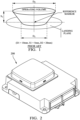
- Typically, the NFC antenna is designed as a loop in a 2D plane and mounted just inside one flat face of a module housing, such that the operating volume (or the area external to the module where devices may connect and communicate with the module) extends above the housing face. The active NFC antenna generates a magnetic field by passing alternating current through the conductive loop. The magnetic field produces an operating volume as shown in
FIG. 2 . This magnetic field can inductively couple with similar antennae found in other devices that are placed within the operating volume. The antennae in these other devices may be connected to active or passive circuitry. Passive devices draw energy from the field generated by the active NFC antenna and communicate with the active NFC antenna by switching in a small load according to NFC protocol, thereby modulating the carrier frequency. - CCC Digital Key is an international standard developed by Car Connectivity Consortium (CCC) for enabling the use of radio frequency identification (RFID) cards, NFC cards, mobile phones, or other electronics devices (key devices) as secure keys for unlocking and starting an automobile or other vehicle. The Digital Key standard utilizes three radio technologies to facilitate the wireless connection between the vehicle and the key device. These are (in order of communication range from farthest to closest): Bluetooth Low Energy (BLE, developed by Bluetooth Special Interest Group), Ultra-wideband (UWB), and NFC. Digital Key devices can utilize a subset of these technologies. NFC has the shortest range and works even if the battery is fully depleted in the Digital Key device. Automotive OEMs may provide Digital Key "cards" as passive NFC cards about the size of a credit card.
- Wireless charging modules (WCM) may utilize NFC functionality for the purposes of RFID/NFC tag detection and protection (these passive devices can potentially be damaged by the wireless charging field if not detected before the wireless charging field is initiated). Additionally, WCM integrated into automotive vehicles may also use NFC for Bluetooth pairing or other automated actions between the mobile device and vehicle. Due to increasing adoption of WCM in vehicles, and increasing demand for Digital Key, WCM are potential applications of Digital Key functionality via NFC. Typically, the NFC antenna is located above a user accessible face of WCM, e.g., the same face that a phone is placed near for wireless charging. Typically, the NFC antenna is built into a printed circuit board mounted near the inside of this face of the module.
- In some aspects, the techniques described herein relate to an electronic module. The electronic module includes a plurality of planar inductive coupling coils configured to interface with a corresponding inductive coupling coil, each inductive coupling coil in the plurality of planar inductive coupling coils being arranged in a different plane than other inductive coupling coils in the plurality of planar inductive coupling coils.
- In some aspects, the techniques described herein relate to a wireless communication module. The wireless communication module includes a first inductive coupling coil configured to generate a first magnetic field having a first axis; and a second inductive coupling coil configured to generate a second magnetic field having a second axis non-coaxial with the first axis.
- The disclosure can be further understood by reference to the following detailed description when considered in connection with the accompanying drawings wherein:
-
FIG. 1 shows an isometric view of an example operating volume of a near field communication (NFC) antenna as defined by the NFC Forum according to the prior art. -
FIG. 2 shows an isometric view of a wireless charging module (WCM) according to some embodiments. -
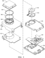
FIG. 3 shows an exploded view of a wireless charging module (WCM) ofFIG. 2 according to some embodiments. -
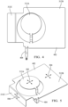
FIG. 4 shows a top view of an NFC antenna array of the WCM ofFIG. 2 in an unfolded form according to some embodiments. -
FIG. 5 shows a top isometric view of the NFC antenna array ofFIG. 4 in a folded form according to some embodiments. -
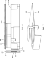
FIG. 6 shows a side view of the WCM ofFIG. 2 with NFC antenna array ofFIG. 5 covering three non-coplanar faces of the WCM according to some embodiments. -
FIG. 7 shows a top isometric view of the folded FPC antenna ofFIG. 6 including a stiffener material on two faces according to some embodiments. -
FIG. 8 shows a bottom isometric view of an FPC antenna ofFIG. 7 according to some embodiments. -
FIG. 9 shows an ideal polarity of two adjacent antennae of the FPC antenna ofFIG. 6 so that the various magnetic fields are additive according to some embodiments. -
FIGs. 10A, 10B, and 10C show side, top, and front views respectively of three distinct regions of operating volume of multiple NFC antennae in the WCM ofFIG. 2 . - Rather than having a single operating volume for a near field communication antenna as shown in
FIG. 1 , it may be advantageous to have multiple operating volumes on multiple faces of a housing of an electronic module. - One non-limiting example of an application of multiple operating volume above multiple faces of a module is incorporated an automotive wireless charging module shown in
FIG. 2 , hereafter referred to as WCM 200. The WCM 200 includes an inductive wireless charging coil which is configured to transfer at least one watt of electrical power to a corresponding inductive wireless charging coil in the consumer device. -
FIG. 3 shows an exploded view of the WCM 200. The WCM 200 includes acap 302 enclosing an array ofalignment magnets 304 and amagnet holder 306. Thecap 302 may provide a surface for charging a consumer device, such as a cellular telephone. The cap may also be configured to retain thealignment magnets 304 and themagnet holder 306 within atower 308 of anupper housing 310. The WCM 200 also includes a plurality of planar inductive coils, hereafter referred to as thecoils 312. The structure and the function of thecoils 312 will be explained in greater detail below. In this example, thecharging coil 314 is formed of Litz wire and is located within thetower 308 of theupper housing 310. Thecharging coil 314 is located adjacent to aferrite 316. Acircuit board 322 containing the electronic circuitry of theWCM 200 is disposed between aninner housing 324 and abottom housing 326, theupper housing 310 being attached to thelower housing 326. - As further shown in
FIG. 4 , thecoils 312 are contained in or on asingle substrate 402. Thecoils 312 are configured for near field communication and are adapted to interface with one or more corresponding inductive coupling coil(s) 610 (seeFIG. 6 ), hereafter referred to as the corresponding coil(s), by establishing near field inductive coupling with the corresponding coil(s) sufficient to support near field communication. For example, the corresponding coils may be contained in the consumer device being wirelessly charged by the WCM and/or a Digital Key device as described above in the BACKGROUND section of this disclosure above. - As shown in
FIG. 4 , each of thecoils coils 312 are configured to support the near field communication in a frequency range of 13.767 MHz to 15.553 MHz and conforms with ISO/IEC Standard 18092:2023. Thesubstrate 402 may be formed of a rigid dielectric material, such as FR4, a flexible dielectric material, such as a flexible printed circuit, a hybrid substrate containing both rigid and flexible dielectric materials, or thesubstrate 402 may be a stamped copper circuit. The coils may be connected to a transceiver by apigtail 404 extending from thesubstrate 402 as shown inFIG. 4 . - As shown in
FIG. 5 , afirst coil 312A is configured to be located in thetower 308 above the charging coil 314 (as shown inFIG. 3 ) and is arranged in afirst plane 502 that is substantially parallel and offset relative to asecond plane 504 of asecond coil 312B. Thefirst coil 312A may be used primarily to establish communication with the consumer device. Thefirst coil 312A may also or alternatively be used to communicate with another device, such as a Digital Key device. Thesecond coil 312B is configured to be located on a surface adjacent to thetower 308 and may be used primarily to establish communication with a Digital Key device. Thesecond coil 312B may also or alternatively be used to communicate with another device, such as the consumer device being wirelessly charged by the WDM. As further shown inFIG. 5 , athird coil 312C is arranged in athird plane 506 that is substantially perpendicular relative to first andsecond planes slot 602 designed to hold aDigital Key 604 is provided near aside surface 606 of theWCM 200 adjacent to thethird coil 312C as shown inFIG. 6 . Theconsumer device 608 is also shown inFIG. 6 positioned near thetower 308 above the chargingcoil 314. -
FIGs. 7 and8 show top and bottom views of thesubstrate 402 with a stiffeningmaterial 702, such as polyimide, metal, or FR4. The stiffeningmaterial 702 contains no electrical circuitry, but only provides mechanical support to thesubstrate 402 where needed, e.g., where components are placed to prevent damage to solder joints during flexing or near a connector interface to provide rigidity for mating and meeting thickness requirements of the connector. - As shown in
FIG. 9 , it may be advantageous to design thecoils coils 312Acoils FIG. 9 , it may also be advantageous to design thecoils coils 312Bcoils - As shown in
FIGs. 10A, 10B, and 10C , thefirst coil 312A generates a first magnetic field having afirst axis 1002 which provides afirst operating volume 1004, thesecond coil 312B generates a second magnetic field having asecond axis 1006 which is non-coaxial with the first axis and provides asecond operating volume 1008, and thethird coil 312C generates a third magnetic field having athird axis 1010 which is perpendicular to the first andsecond axes third operating volume 1012. Thesecond operating volume 1008 is laterally offset from thefirst operating volume 1004. - In alternative embodiments, any one of the
coils - The example of a near field antenna array on multiple faces of a module is shown here in the context an automotive wireless charging module, but other embodiments may be envisioned for other type of electronic modules that contains an NFC antenna where it would be advantageous to have operating volumes above more than one face of the module (e.g., payment kiosk, stand-alone digital key reader module, etc.).
- The following are non-exclusive descriptions of possible embodiments of the present invention.
- In some aspects, the techniques described herein relate to an electronic module. The electronic module includes a plurality of planar inductive coupling coils configured to interface with a corresponding inductive coupling coil, each inductive coupling coil in the plurality of planar inductive coupling coils being arranged in a different plane than other inductive coupling coils in the plurality of planar inductive coupling coils.
- The electronic module of the preceding paragraph can optionally include, additionally and/or alternatively any, one or more of the following features, configurations and/or additional components.
- In some aspects, the techniques described herein relate to an electronic module, wherein the plurality of planar inductive coupling coils is configured to establish inductive coupling with the corresponding coil sufficient to support near field communication.
- In some aspects, the techniques described herein relate to an electronic module, wherein the plurality of planar inductive coupling coils is configured to establish inductive coupling with the corresponding coil sufficient to support the near field communication in a frequency range of 13.767 MHz to 15.553 MHz.
- In some aspects, the techniques described herein relate to an electronic module, wherein the near field communication conforms with ISO/IEC Standard 18092:2023.
- In some aspects, the techniques described herein relate to an electronic module, wherein at least one of the coils in the plurality of planar inductive coupling coils and the corresponding coil are configured to establish inductive coupling sufficient to support the near field communication at a distance up to four centimeters.
- In some aspects, the techniques described herein relate to an electronic module, wherein a single substrate includes the plurality of planar inductive coupling coils.
- In some aspects, the techniques described herein relate to an electronic module, wherein the single substrate is formed of a flexible dielectric material.
- In some aspects, the techniques described herein relate to an electronic module, wherein the plurality of planar inductive coupling coils is formed by a stamped copper circuit.
- In some aspects, the techniques described herein relate to an electronic module, further including an inductive charging transmitter coil configured to transmit more than one watt of electrical power to an inductive charging receiver coil.
- In some aspects, the techniques described herein relate to an electronic module, wherein one inductive coupling coil in the plurality of planar inductive coupling coils is arranged in a plane that is substantially perpendicular relative to planes of other inductive coupling coils in the plurality of planar inductive coupling coils.
- In some aspects, the techniques described herein relate to an electronic module, wherein one inductive coupling coil in the plurality of planar inductive coupling coils is arranged in a plane that is substantially parallel and offset relative to planes of other inductive coupling coils in the plurality of planar inductive coupling coils.
- In some aspects, the techniques described herein relate to a wireless communication module. The wireless communication module includes a first inductive coupling coil configured to generate a first magnetic field having a first axis; and a second inductive coupling coil configured to generate a second magnetic field having a second axis non-coaxial with the first axis.
- The wireless communication module of the preceding paragraph can optionally include, additionally and/or alternatively any, one or more of the following features, configurations and/or additional components.
- In some aspects, the techniques described herein relate to a wireless communication module, wherein the second axis of the second coil is laterally offset from the first axis of the first coil.
- In some aspects, the techniques described herein relate to a wireless communication module, wherein the first axis of the first coil is substantially perpendicular to the second axis of the second coil.
- In some aspects, the techniques described herein relate to a wireless communication module, wherein at least one of the first and second inductive coupling coils are configured to transmit up to one watt of electrical power.
- In some aspects, the techniques described herein relate to a wireless communication module, wherein a single substrate includes the first and second inductive coupling coils.
- In some aspects, the techniques described herein relate to a wireless communication module, further including a third inductive coupling coil configured to generate a third magnetic field having a third axis laterally offset from the first axis of the first coil and substantially perpendicular to the second axis of the second coil.
- In some aspects, the techniques described herein relate to a wireless communication module, further including a third inductive coupling coil configured to generate a third magnetic field having a third axis coaxial with the first axis of the first coil.
- In some aspects, the techniques described herein relate to a wireless communication module, wherein the third coil is configured to transmit more than one watt of electrical power.
- In some aspects, the techniques described herein relate to a wireless communication module, wherein the first and second inductive coupling coils are contained in a single substrate.
- While the invention has been described with reference to an exemplary embodiment(s), it will be understood by those skilled in the art that various changes may be made, and equivalents may be substituted for elements thereof without departing from the scope of the invention. In addition, many modifications may be made to adapt a particular situation or material to the teachings of the invention without departing from the essential scope thereof. Therefore, it is intended that the invention is not limited to the disclosed embodiment(s), but that the invention will include all embodiments falling within the scope of the appended claims.
- As used herein, 'one or more' includes a function being performed by one element, a function being performed by more than one element, e.g., in a distributed fashion, several functions being performed by one element, several functions being performed by several elements, or any combination of the above.
- It will also be understood that, although the terms first, second, etc. are, in some instances, used herein to describe various elements, these elements should not be limited by these terms. These terms are only used to distinguish one element from another. For example, a first contact could be termed a second contact, and, similarly, a second contact could be termed a first contact, without departing from the scope of the various described embodiments. The first contact and the second contact are both contacts, but they are not the same contact.
- The terminology used in the description of the various described embodiments herein is for the purpose of describing particular embodiments only and is not intended to be limiting. As used in the description of the various described embodiments and the appended claims, the singular forms "a", "an" and "the" are intended to include the plural forms as well, unless the context clearly indicates otherwise. It will also be understood that the term "and/or" as used herein refers to and encompasses any and all possible combinations of one or more of the associated listed items. It will be further understood that the terms "includes," "including," "comprises," and/or "comprising," when used in this specification, specify the presence of stated features, integers, steps, operations, elements, and/or components, but do not preclude the presence or addition of one or more other features, integers, steps, operations, elements, components, and/or groups thereof.
- As used herein, the term "if' is, optionally, construed to mean "when" or "upon" or "in response to determining" or "in response to detecting," depending on the context. Similarly, the phrase "if it is determined" or "if [a stated condition or event] is detected" is, optionally, construed to mean "upon determining" or "in response to determining" or "upon detecting [the stated condition or event]" or "in response to detecting [the stated condition or event]," depending on the context.
- Additionally, while terms of ordinance or orientation may be used herein these elements should not be limited by these terms. All terms of ordinance or orientation, unless stated otherwise, are used for purposes distinguishing one element from another, and do not denote any particular order, order of operations, direction or orientation unless stated otherwise.
Claims (15)
- An electronic module (200), comprising:
a plurality of planar inductive coupling coils (312A, 312B, 312C) configured to interface with a corresponding inductive coupling coil (610), each planar inductive coupling coil in the plurality of planar inductive coupling coils (312A, 312B, 312C) being arranged in a different plane than other planar inductive coupling coils (312A, 312B, 312C) in the plurality of planar inductive coupling coils (312A, 312B, 312C). - The electronic module (200) according to claim 1, wherein the plurality of planar inductive coupling coils (312A, 312B, 312C) is configured to establish inductive coupling with the corresponding coil (610) sufficient to support near field communication.
- The electronic module (200) according to claim 2, wherein the plurality of planar inductive coupling coils (312A, 312B, 312C) is configured to establish inductive coupling with the corresponding coil (610) sufficient to support the near field communication in a frequency range of 13.767 MHz to 15.553 MHz.
- The electronic module (200) according to claim 2 or 3, wherein the near field communication conforms with ISO/IEC Standard 18092:2023.
- The electronic module (200) according to any one of claims 2 to 4, wherein at least one of the coils (312A, 312B, 312C) in the plurality of planar inductive coupling coils (312A, 312B, 312C) and the corresponding coil (610) are configured to establish inductive coupling sufficient to support the near field communication at a distance up to four centimeters.
- The electronic module (200) according to any one of the preceding claims, wherein a single substrate (402) comprises the plurality of planar inductive coupling coils (312A, 312B, 312C).
- The electronic module (200) according to claim 6, wherein the single substrate (402) is formed of a flexible dielectric material.
- The electronic module (200) according to any one of the preceding claims, further comprising an inductive wireless charging coil (314) configured to transmit more than one watt of electrical power to a corresponding inductive wireless charging coil.
- The electronic module (200) according to any one of the preceding claims, wherein one inductive coupling coil (312C) in the plurality of planar inductive coupling coils (312A, 312B, 312C) is arranged in a plane that is substantially perpendicular relative to planes of other inductive coupling coils (312A, 312B) in the plurality of planar inductive coupling coils (312A, 312B, 312C).
- The electronic module (200) according to any one of the preceding claims, wherein one inductive coupling coil in the plurality of planar inductive coupling coils (312A) is arranged in a plane that is substantially parallel and offset relative to planes of other inductive coupling coils (312B) in the plurality of planar inductive coupling coils (312A, 312B, 312C).
- A wireless communication module (200), comprising:a first inductive coupling coil (312A) configured to generate a first magnetic field (1004) having a first axis (1002); anda second inductive coupling coil (312B, 312C) configured to generate a second magnetic field (1008, 1012) having a second axis (1006, 1010) non-coaxial with the first axis (1002).
- The wireless communication module (200) according to claim 11, wherein the second axis (1006) of the second coil (312B) is laterally offset from the first axis (1002) of the first inductive coupling coil (312A).
- The wireless communication module (200) according to claim 11 or 12, wherein the first axis (1002) of the first coil (312A) is substantially perpendicular to the second axis (1010) of the second coil (312C).
- The wireless communication module (200) according to any one of claims 11 to 13, wherein at least one of the first and second inductive coupling coils (312A, 312B, 312C) are configured to transmit up to one watt of electrical power.
- The wireless communication module (200) according to any one of claims 11 to 14, wherein a single substrate (402) comprises the first and second inductive coupling coils (312A, 312B, 312C).
Applications Claiming Priority (2)
| Application Number | Priority Date | Filing Date | Title |
|---|---|---|---|
| US202363545791P | 2023-10-26 | 2023-10-26 | |
| US18/905,306 US20250141495A1 (en) | 2023-10-26 | 2024-10-03 | Multi-plane inductive coupling coil array for electronic module |
Publications (1)
| Publication Number | Publication Date |
|---|---|
| EP4546657A1 true EP4546657A1 (en) | 2025-04-30 |
Family
ID=93213776
Family Applications (1)
| Application Number | Title | Priority Date | Filing Date |
|---|---|---|---|
| EP24207787.3A Pending EP4546657A1 (en) | 2023-10-26 | 2024-10-21 | Multilevel coil array with inductive coupling for an electronic module |
Country Status (3)
| Country | Link |
|---|---|
| US (1) | US20250141495A1 (en) |
| EP (1) | EP4546657A1 (en) |
| CN (1) | CN119906458A (en) |
Citations (4)
| Publication number | Priority date | Publication date | Assignee | Title |
|---|---|---|---|---|
| US20110306296A1 (en) * | 2010-06-11 | 2011-12-15 | Sony Corporation | Communication device |
| US20160142866A1 (en) * | 2014-11-13 | 2016-05-19 | Yo-Han JANG | Near field communication chip embedded in a wearable electronic device and wearable electronic device |
| US20190028149A1 (en) * | 2015-12-23 | 2019-01-24 | Datalogic Ip Tech S.R.L. | Coexistence of wireless charging and near field communication in a portable data terminal |
| EP3667631A1 (en) * | 2018-12-12 | 2020-06-17 | Graphene Security Limited | High-frequency-nfc-based product traceability and anti-counterfeiting tag |
-
2024
- 2024-10-03 US US18/905,306 patent/US20250141495A1/en active Pending
- 2024-10-18 CN CN202411459994.3A patent/CN119906458A/en active Pending
- 2024-10-21 EP EP24207787.3A patent/EP4546657A1/en active Pending
Patent Citations (4)
| Publication number | Priority date | Publication date | Assignee | Title |
|---|---|---|---|---|
| US20110306296A1 (en) * | 2010-06-11 | 2011-12-15 | Sony Corporation | Communication device |
| US20160142866A1 (en) * | 2014-11-13 | 2016-05-19 | Yo-Han JANG | Near field communication chip embedded in a wearable electronic device and wearable electronic device |
| US20190028149A1 (en) * | 2015-12-23 | 2019-01-24 | Datalogic Ip Tech S.R.L. | Coexistence of wireless charging and near field communication in a portable data terminal |
| EP3667631A1 (en) * | 2018-12-12 | 2020-06-17 | Graphene Security Limited | High-frequency-nfc-based product traceability and anti-counterfeiting tag |
Also Published As
| Publication number | Publication date |
|---|---|
| CN119906458A (en) | 2025-04-29 |
| US20250141495A1 (en) | 2025-05-01 |
Similar Documents
| Publication | Publication Date | Title |
|---|---|---|
| US10367267B2 (en) | Flexible printed circuit board for dual mode antennas, dual mode antenna and user device | |
| KR101488607B1 (en) | Antenna structure for near field communication | |
| US9692128B2 (en) | Antenna device and wireless communication device | |
| EP1500167B1 (en) | Energy source communication employing slot antenna | |
| CN101719558B (en) | Battery pack and information processing apparatus | |
| KR101052115B1 (en) | NFC Antenna Using Double Resonance | |
| US9865913B2 (en) | Communication terminal and card antenna module | |
| US20100093412A1 (en) | Protective envelope for a handheld electronic device | |
| EP3576248B1 (en) | Nfc reader | |
| CN103814477B (en) | Antenna device and communication device | |
| KR102194806B1 (en) | Wireless antenna for wireless charging and nfc communication, and wireless device having the same | |
| EP2302568A2 (en) | Antenna device | |
| US20120182128A1 (en) | Communication terminal and information processing system | |
| US20140320355A1 (en) | Antenna apparatus and communication apparatus | |
| CN109755728A (en) | NFC antenna equipment in metal environment | |
| US9837700B2 (en) | Antenna device and portable electronic device | |
| KR20140134238A (en) | Nfc antenna module and portable terminal device having the same | |
| US20250141495A1 (en) | Multi-plane inductive coupling coil array for electronic module | |
| WO2009030986A1 (en) | Sim connector with ferrite | |
| CN216120746U (en) | NFC coupling antenna | |
| US20240039342A1 (en) | Wireless charging device with nfc function | |
| EP3709524A1 (en) | Antenna device and associated apparatus |
Legal Events
| Date | Code | Title | Description |
|---|---|---|---|
| PUAI | Public reference made under article 153(3) epc to a published international application that has entered the european phase |
Free format text: ORIGINAL CODE: 0009012 |
|
| STAA | Information on the status of an ep patent application or granted ep patent |
Free format text: STATUS: THE APPLICATION HAS BEEN PUBLISHED |
|
| AK | Designated contracting states |
Kind code of ref document: A1 Designated state(s): AL AT BE BG CH CY CZ DE DK EE ES FI FR GB GR HR HU IE IS IT LI LT LU LV MC ME MK MT NL NO PL PT RO RS SE SI SK SM TR |
|
| STAA | Information on the status of an ep patent application or granted ep patent |
Free format text: STATUS: REQUEST FOR EXAMINATION WAS MADE |
|
| 17P | Request for examination filed |
Effective date: 20250822 |