EP4546656A2 - Electronic apparatus - Google Patents
Electronic apparatus Download PDFInfo
- Publication number
- EP4546656A2 EP4546656A2 EP24197233.0A EP24197233A EP4546656A2 EP 4546656 A2 EP4546656 A2 EP 4546656A2 EP 24197233 A EP24197233 A EP 24197233A EP 4546656 A2 EP4546656 A2 EP 4546656A2
- Authority
- EP
- European Patent Office
- Prior art keywords
- circuit board
- field communication
- antenna
- communication antenna
- printed circuit
- Prior art date
- Legal status (The legal status is an assumption and is not a legal conclusion. Google has not performed a legal analysis and makes no representation as to the accuracy of the status listed.)
- Pending
Links
Images







Classifications
-
- H—ELECTRICITY
- H01—ELECTRIC ELEMENTS
- H01Q—ANTENNAS, i.e. RADIO AERIALS
- H01Q1/00—Details of, or arrangements associated with, antennas
- H01Q1/12—Supports; Mounting means
- H01Q1/22—Supports; Mounting means by structural association with other equipment or articles
- H01Q1/24—Supports; Mounting means by structural association with other equipment or articles with receiving set
- H01Q1/241—Supports; Mounting means by structural association with other equipment or articles with receiving set used in mobile communications, e.g. GSM
- H01Q1/242—Supports; Mounting means by structural association with other equipment or articles with receiving set used in mobile communications, e.g. GSM specially adapted for hand-held use
- H01Q1/243—Supports; Mounting means by structural association with other equipment or articles with receiving set used in mobile communications, e.g. GSM specially adapted for hand-held use with built-in antennas
-
- H—ELECTRICITY
- H04—ELECTRIC COMMUNICATION TECHNIQUE
- H04B—TRANSMISSION
- H04B5/00—Near-field transmission systems, e.g. inductive or capacitive transmission systems
- H04B5/20—Near-field transmission systems, e.g. inductive or capacitive transmission systems characterised by the transmission technique; characterised by the transmission medium
- H04B5/24—Inductive coupling
- H04B5/26—Inductive coupling using coils
-
- H—ELECTRICITY
- H01—ELECTRIC ELEMENTS
- H01Q—ANTENNAS, i.e. RADIO AERIALS
- H01Q1/00—Details of, or arrangements associated with, antennas
- H01Q1/36—Structural form of radiating elements, e.g. cone, spiral, umbrella; Particular materials used therewith
- H01Q1/38—Structural form of radiating elements, e.g. cone, spiral, umbrella; Particular materials used therewith formed by a conductive layer on an insulating support
-
- G—PHYSICS
- G04—HOROLOGY
- G04G—ELECTRONIC TIME-PIECES
- G04G17/00—Structural details; Housings
- G04G17/02—Component assemblies
-
- G—PHYSICS
- G04—HOROLOGY
- G04G—ELECTRONIC TIME-PIECES
- G04G17/00—Structural details; Housings
- G04G17/02—Component assemblies
- G04G17/04—Mounting of electronic components
-
- G—PHYSICS
- G04—HOROLOGY
- G04G—ELECTRONIC TIME-PIECES
- G04G17/00—Structural details; Housings
- G04G17/02—Component assemblies
- G04G17/04—Mounting of electronic components
- G04G17/045—Mounting of the display
-
- G—PHYSICS
- G04—HOROLOGY
- G04R—RADIO-CONTROLLED TIME-PIECES
- G04R60/00—Constructional details
- G04R60/06—Antennas attached to or integrated in clock or watch bodies
-
- G—PHYSICS
- G04—HOROLOGY
- G04R—RADIO-CONTROLLED TIME-PIECES
- G04R60/00—Constructional details
- G04R60/06—Antennas attached to or integrated in clock or watch bodies
- G04R60/10—Antennas attached to or integrated in clock or watch bodies inside cases
-
- H—ELECTRICITY
- H01—ELECTRIC ELEMENTS
- H01Q—ANTENNAS, i.e. RADIO AERIALS
- H01Q1/00—Details of, or arrangements associated with, antennas
- H01Q1/12—Supports; Mounting means
- H01Q1/22—Supports; Mounting means by structural association with other equipment or articles
-
- H—ELECTRICITY
- H01—ELECTRIC ELEMENTS
- H01Q—ANTENNAS, i.e. RADIO AERIALS
- H01Q1/00—Details of, or arrangements associated with, antennas
- H01Q1/27—Adaptation for use in or on movable bodies
- H01Q1/273—Adaptation for carrying or wearing by persons or animals
-
- H—ELECTRICITY
- H01—ELECTRIC ELEMENTS
- H01Q—ANTENNAS, i.e. RADIO AERIALS
- H01Q7/00—Loop antennas with a substantially uniform current distribution around the loop and having a directional radiation pattern in a plane perpendicular to the plane of the loop
-
- H—ELECTRICITY
- H04—ELECTRIC COMMUNICATION TECHNIQUE
- H04B—TRANSMISSION
- H04B5/00—Near-field transmission systems, e.g. inductive or capacitive transmission systems
- H04B5/40—Near-field transmission systems, e.g. inductive or capacitive transmission systems characterised by components specially adapted for near-field transmission
- H04B5/43—Antennas
-
- H—ELECTRICITY
- H05—ELECTRIC TECHNIQUES NOT OTHERWISE PROVIDED FOR
- H05K—PRINTED CIRCUITS; CASINGS OR CONSTRUCTIONAL DETAILS OF ELECTRIC APPARATUS; MANUFACTURE OF ASSEMBLAGES OF ELECTRICAL COMPONENTS
- H05K1/00—Printed circuits
- H05K1/02—Details
- H05K1/14—Structural association of two or more printed circuits
- H05K1/147—Structural association of two or more printed circuits at least one of the printed circuits being bent or folded, e.g. by using a flexible printed circuit
-
- H—ELECTRICITY
- H05—ELECTRIC TECHNIQUES NOT OTHERWISE PROVIDED FOR
- H05K—PRINTED CIRCUITS; CASINGS OR CONSTRUCTIONAL DETAILS OF ELECTRIC APPARATUS; MANUFACTURE OF ASSEMBLAGES OF ELECTRICAL COMPONENTS
- H05K1/00—Printed circuits
- H05K1/16—Printed circuits incorporating printed electric components, e.g. printed resistors, capacitors or inductors
- H05K1/165—Printed circuits incorporating printed electric components, e.g. printed resistors, capacitors or inductors incorporating printed inductors
-
- H—ELECTRICITY
- H05—ELECTRIC TECHNIQUES NOT OTHERWISE PROVIDED FOR
- H05K—PRINTED CIRCUITS; CASINGS OR CONSTRUCTIONAL DETAILS OF ELECTRIC APPARATUS; MANUFACTURE OF ASSEMBLAGES OF ELECTRICAL COMPONENTS
- H05K1/00—Printed circuits
- H05K1/18—Printed circuits structurally associated with non-printed electric components
-
- H—ELECTRICITY
- H05—ELECTRIC TECHNIQUES NOT OTHERWISE PROVIDED FOR
- H05K—PRINTED CIRCUITS; CASINGS OR CONSTRUCTIONAL DETAILS OF ELECTRIC APPARATUS; MANUFACTURE OF ASSEMBLAGES OF ELECTRICAL COMPONENTS
- H05K1/00—Printed circuits
- H05K1/18—Printed circuits structurally associated with non-printed electric components
- H05K1/189—Printed circuits structurally associated with non-printed electric components characterised by the use of flexible or folded printed circuits
-
- H—ELECTRICITY
- H05—ELECTRIC TECHNIQUES NOT OTHERWISE PROVIDED FOR
- H05K—PRINTED CIRCUITS; CASINGS OR CONSTRUCTIONAL DETAILS OF ELECTRIC APPARATUS; MANUFACTURE OF ASSEMBLAGES OF ELECTRICAL COMPONENTS
- H05K2201/00—Indexing scheme relating to printed circuits covered by H05K1/00
- H05K2201/10—Details of components or other objects attached to or integrated in a printed circuit board
- H05K2201/10007—Types of components
- H05K2201/10098—Components for radio transmission, e.g. radio frequency identification [RFID] tag, printed or non-printed antennas
-
- H—ELECTRICITY
- H05—ELECTRIC TECHNIQUES NOT OTHERWISE PROVIDED FOR
- H05K—PRINTED CIRCUITS; CASINGS OR CONSTRUCTIONAL DETAILS OF ELECTRIC APPARATUS; MANUFACTURE OF ASSEMBLAGES OF ELECTRICAL COMPONENTS
- H05K2201/00—Indexing scheme relating to printed circuits covered by H05K1/00
- H05K2201/10—Details of components or other objects attached to or integrated in a printed circuit board
- H05K2201/10007—Types of components
- H05K2201/10128—Display
-
- H—ELECTRICITY
- H05—ELECTRIC TECHNIQUES NOT OTHERWISE PROVIDED FOR
- H05K—PRINTED CIRCUITS; CASINGS OR CONSTRUCTIONAL DETAILS OF ELECTRIC APPARATUS; MANUFACTURE OF ASSEMBLAGES OF ELECTRICAL COMPONENTS
- H05K2201/00—Indexing scheme relating to printed circuits covered by H05K1/00
- H05K2201/10—Details of components or other objects attached to or integrated in a printed circuit board
- H05K2201/10007—Types of components
- H05K2201/10189—Non-printed connector
Definitions
- One or more embodiments relate to an electronic apparatus, and more particularly, to an electronic apparatus having a simple structure and capable of near-field communication.
- an electronic apparatus such as a smartwatch or a smartphone includes a display panel.
- the electronic apparatus also includes a wireless communication antenna to communicate wirelessly with external devices.
- a wireless communication antenna to communicate wirelessly with external devices.
- an increasing number of electronic apparatuses include an antenna for near-field communication.
- the electronic apparatus includes a flexible printed circuit board for generating or transmitting electrical signals to be applied to the display panel.
- one or more embodiments include an electronic apparatus having a simplified or streamlined structure and capable of near-field communication.
- an electronic apparatus having a simplified or streamlined structure and capable of near-field communication.
- such a technical problem is an example, and one or more embodiments are not limited thereto.
- an electronic apparatus includes a light-transmitting window, a display panel disposed over the light-transmitting window, a printed circuit board electrically connected to the display panel, disposed over a side of the display panel to face away from the light-transmitting window, and including wires and a near-field communication antenna, and a main circuit board electrically connected to the printed circuit board and disposed over a side of the printed circuit board to face away from the display panel.
- the printed circuit board may include an antenna area and a peripheral area outside the antenna area, and the near-field communication antenna may be disposed in the antenna area.
- the wires may not be disposed in the antenna area except for one or more of the wires electrically connected to the near-field communication antenna.
- wires other than one or more of the wires electrically connected to the near-field communication antenna may be in the peripheral area.
- the electronic apparatus may further include a cover panel between the display panel and the printed circuit board.
- the cover panel may include a cushion layer and a metal layer, and the metal layer may include a transmissive opening.
- the transmissive opening When viewed in a direction perpendicular to the display panel, the transmissive opening may overlap the antenna area.
- an area of the transmissive opening When viewed in the direction perpendicular to the display panel, an area of the transmissive opening may be substantially equal to or greater than an area of the antenna area.
- the printed circuit board may include a first connector electrically connected to at least one of the wires and the near-field communication antenna, and the main circuit board may include a first main connector electrically connected to the first connector.
- the printed circuit board may include a first connector electrically connected to at least one of the wires and a second connector electrically connected to the near-field communication antenna, and the main circuit board may include a first main connector electrically connected to the first connector and a second main connector electrically connected to the second connector.
- the electronic apparatus may further include a first terminal electrically connected to an end of the near-field communication antenna, the first terminal and the near-field communication antenna being disposed on a same layer, and a second terminal electrically connected to another end of the near-field communication antenna, the second terminal and the near-field communication antenna being disposed on different layers.
- the first terminal and the near-field communication antenna may be integral with each other.
- the electronic apparatus may further include a first terminal disposed on a layer electrically connected to an end of the near-field communication antenna, the first terminal and the near-field communication antenna being disposed on a same layer, an additional antenna having an end electrically connected to another end of the near-field communication antenna, the additional antenna and the near-field communication antenna being disposed on different layers, and a second terminal electrically connected to another end of the additional antenna.
- the first terminal and the near-field communication antenna may be integral with each other.
- the second terminal and the first terminal may be disposed on a same layer.
- an electronic apparatus includes a light-transmitting window, a display panel disposed over the light-transmitting window, a printed circuit board electrically connected to the display panel, disposed over a side of the display panel to face away from the light-transmitting window, and including wires that transmit an electrical signal to be applied to the display panel, and a main circuit board electrically connected to the printed circuit board, disposed over a side of the printed circuit board to face away from the display panel, and including wires and a near-field communication antenna.
- the main circuit board may include an antenna area and a peripheral area outside the antenna area, and the near-field communication antenna may be disposed in the antenna area.
- the wires may not be disposed in the antenna area except for one or more of the wires electrically connected to the near-field communication antenna.
- wires other than one or more of the wires electrically connected to the near-field communication antenna may be in the peripheral area.
- the electronic apparatus may further include a cover panel between the display panel and the printed circuit board and including a cushion layer and a metal layer, wherein the metal layer may include a transmissive opening.
- the transmissive opening When viewed in a direction perpendicular to the display panel, the transmissive opening may overlap the antenna area, and the wires in the printed circuit board may overlap the peripheral area.
- an area of the transmissive opening When viewed in the direction perpendicular to the display panel, an area of the transmissive opening may be substantially equal to or greater than an area of the antenna area.
- the phrase "at least one of A and B" may be construed as A only, B only, or any combination of A and B.
- “at least one of X, Y, and Z” and “at least one selected from the group consisting of X, Y, and Z” may be construed as X only, Y only, Z only, or any combination of two or more of X, Y, and Z.
- the x-axis, the y-axis, and the z-axis are not limited to three axes of the rectangular coordinate system and may be interpreted in a broader sense.
- the x-axis, the y-axis, and the z-axis may be perpendicular to one another or may represent different directions that are not perpendicular to one another.
- layers, regions, or elements when layers, regions, or elements are referred to as being connected to each other, they may be directly connected to each other or may be indirectly connected to each other with intervening layers, regions, or elements therebetween.
- layers, regions, or elements when layers, regions, or elements are referred to as being electrically connected to each other, they may be directly electrically connected to each other or may be indirectly electrically connected to each other with intervening layers, regions, or elements therebetween.
- FIG. 1 is a schematic exploded perspective view of a portion of an electronic apparatus according to an embodiment.
- FIG. 2 is a perspective view schematically showing some elements shown in FIG. 1 which are stacked on each other.
- FIG. 3 is a perspective view schematically showing some elements shown in FIG. 2 which are bent.
- the electronic apparatus may include a window 10, a display panel 30, a printed circuit board 40, and/or a main circuit board 60.
- the electronic apparatus may further include various elements as shown in FIG. 1 .
- the electronic apparatus may further include a cover panel 50 disposed between the display panel 30 and the printed circuit board 40.
- the electronic apparatus may further include a back cover (not shown) coupled to the window 10 to allow various elements to be positioned inside.
- Examples of the electronic apparatus may include various electronics such as a smartwatch, a smartphone, and/or a tablet.
- the window 10 may be formed of a light-transmitting material and may include glass or polymer resin.
- the window 10 may include, for example, polymer resin such as polyethersulfone, polyacrylate, polyetherimide, polyethylene naphthalate, polyethylene terephthalate, polyphenylene sulfide, polyarylate, polyimide, polycarbonate, or cellulose acetate propionate.
- the window 10 may include a base 11 and an edge portion 13.
- the base 11 may determine the overall appearance of the window 10 and transmit light.
- the edge portion 13 may protrude from a first virtual plane on (or in) which the base 11 is located.
- FIG. 1 shows that the base 11 may be located on the first virtual plane that is approximately parallel to an x-y plane and the edge portion 13 may protrude from an edge of the base 11 approximately in a direction (e.g., +z direction) perpendicular to the x-y plane.
- the base 11 and the edge portion 13 may include a same material and may be integrally formed as a single body (or integral with each other), but one or more embodiments are not limited thereto.
- the edge portion 13 may be a separate element from the base 11 and may be coupled to the edge of the base 11. In this case, the edge portion 13 may be non-transmissive, unlike the light-transmitting base 11.
- the base 11 may be located in the first virtual plane, and the first plane may be curved.
- the base 11 included in the window 10 may have a flat shape as a whole, but an outer surface of the base 11 opposite to the display panel 30 (i.e., the outer surface in -z direction) may include a portion that is microscopically curved.
- the display panel 30 may be disposed on the base 11 of the window 10.
- the display panel 30 may include a circuit that includes an electronic device such as a thin-film transistor on a substrate, and a display element such as an organic or inorganic light-emitting diode electrically connected to the circuit.
- an electronic device such as a thin-film transistor on a substrate
- a display element such as an organic or inorganic light-emitting diode electrically connected to the circuit.
- the display panel 30 may include various display elements such as a liquid crystal device instead of the organic light-emitting diode.
- the printed circuit board 40 may be flexible.
- the printed circuit board 40 may be electrically connected to the display panel 30.
- a portion of the printed circuit board 40 may be attached onto and/or electrically connected onto a surface of the display panel 30 in a direction toward the window 10.
- wires or pads of the printed circuit board 40 may be electrically connected to pads positioned on the surface of the display panel 30 in a direction toward the window 10 through an anisotropic conductive film, etc.
- the printed circuit board 40 may include a body portion 41, a neck portion 43 protruding from the body portion 41, and/or a first connecting portion 45 protruding from the body portion 41.
- the neck portion 43 may be in contact with the display panel 30 as described above.
- the body portion 41 may have an area greater than that of the neck portion 43, and an electronic device such as an integrated circuit may be attached to the body portion 41 of the printed circuit board 40 through an anisotropic conductive film, etc.
- Pads electrically connected to an electronic device may be positioned in the body portion 41, and wires extending to the neck portion 43 and/or the first connecting portion 45 may also be positioned in the body portion 41. Electrical signals to be applied to the display panel 30 may be transmitted through the wires.
- a near-field communication antenna ATN (refer to FIG. 5 ) may be positioned at the body portion 41.
- a first connector 40c1 may be positioned at the first connecting portion 45, and wires extending from the body portion 41 may be electrically connected to the first connector 40c 1.
- the cover panel 50 may be disposed between the display panel 30 and the printed circuit board 40. A detailed description of the cover panel 50 is given below.
- the display panel 30 and the cover panel 50 may be on the window 10 as shown in FIG. 2 .
- the display panel 30 and the cover panel 50 may be positioned inside a space defined by the base 11 and the edge portion 13 of the window 10.
- the printed circuit board 40 electrically connected to the display panel 30 may be bent at the neck portion 43 as shown in FIG. 3 , and thus, the body portion 41 may be placed on the cover panel 50.
- the printed circuit board 40 may be flexible as described above, the neck portion 43 may be flexible and may be bent as shown in FIGS. 2 and 3 , and the body portion 41 may be placed on the cover panel 50. In some cases, the body portion 41 may also be flexible. In this case, the neck portion 43 may be more flexible than the body portion 41.
- the printed circuit board 40 having the neck portion 43 electrically connected to the display panel 30 as described above may be bent at the neck portion 43, and the body portion 41 may be disposed over a side of the display panel 30 to face away from the window 10 (e.g., may be disposed in the +z direction from the display panel 30). It may be understood as describing that the printed circuit board 40 is opposite to the window 10 (in the +z direction) with respect to the display panel 30.
- the main circuit board 60 may be on the printed circuit board 40 having the neck portion 43 bent.
- the main circuit board 60 may be electrically connected to the printed circuit board 40 and may be disposed over a side of the printed circuit board 40 to face away from the display panel 30 (e.g., may be disposed in the +z direction from the printed circuit board 40).
- Electronic elements such as an application processor (AP) or a central processing unit (CPU) of an electronic apparatus may be on the main circuit board 60, and wires configured to transmit an electrical signal from those electronic elements or an electrical signal to those electronic elements may also be on the main circuit board 60.
- the main circuit board 60 may not be flexible unlike the printed circuit board 40.
- the main circuit board 60 may include a first main connector 60c1, and the first connector 40c1 of the printed circuit board 40 may be fastened to the first main connector 60c 1 of the main circuit board 60 to electrically connect the printed circuit board 40 to the main circuit board 60.
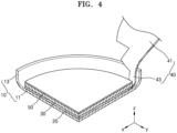
- FIG. 4 is a perspective view schematically showing a shape of a portion of the electronic apparatus of FIG. 1 during a process of manufacturing the electronic apparatus of FIG. 1 .
- the display panel 30 and the cover panel 50 are placed in a space defined by the base 11 and the edge portion 13 of the window 10, and then, the printed circuit board 40 is bent at the neck portion 43 to place the body portion 41 of the printed circuit board 40 on the display panel 30 and the cover panel 50.
- FIG. 4 may be understood as showing a process of placing the display panel 30 and the cover panel 50 in a space defined by the base 11 and the edge portion 13 of the window 10 during a process of manufacturing the electronic apparatus.
- a light-transmitting adhesive layer 20 may be disposed between the window 10 and the display panel 30 to bond the window 10 and the display panel 30.
- FIG. 5 is a schematic plan view of the printed circuit board 40 of the electronic apparatus of FIG. 1 .
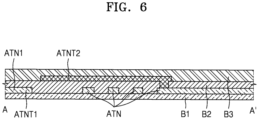
- FIG. 6 is a schematic cross-sectional view of the printed circuit board 40 of FIG. 5 , taken along a line A-A' of FIG. 5 .
- the printed circuit board 40 includes the near-field communication antenna ATN.
- the printed circuit board 40 may have an antenna area 41a and a peripheral area outside the antenna area 41a.
- the near-field communication antenna ATN may be in the antenna area 41a.
- the antenna area 41a may be positioned at the body portion 41 of the printed circuit board 40.
- the near-field communication antenna ATN may be arranged in a form of a coil in a plane (e.g., the x-y plane) where the printed circuit board 40 is disposed.
- the near-field communication antenna ATN is illustrated as having a shape like a wire extending from the outside to the inside while rotating clockwise.
- embodiments are not limited thereto, and the near-field communication antenna ATN may have different shapes within the scope of the disclosure.
- a first terminal ATNT1 may be electrically connected to an end of the near-field communication antenna ATN, and a second terminal ATNT2 may be electrically connected to another end of the near-field communication antenna ATN.
- Each of the first terminal ATNT1 and the second terminal ATNT2 may be, for example, a portion of a wire.
- FIGS. 5 and 6 show that the first terminal ATNT1 may be disposed on a layer on which the near-field communication antenna ATN may be disposed such that the first terminal ATNT1 and the near-field communication antenna ATN are integrally formed as a single body, and the second terminal ATNT2 may be disposed on a layer different from the layer on which the near-field communication antenna ATN may be disposed.
- the printed circuit board 40 may have a structure in which a first base B1, a second base B2, and a third base B3, which are insulating layers including a resin (e.g., polyimide or a similar resin), are sequentially stacked on one another, and the near-field communication antenna ATN and the first terminal ATNT1 may be disposed between the first base B1 and the second base B2, and the second terminal ATNT2 may be disposed between the second base B2 and the third base B3 and may be in contact with the another end of the near-field communication antenna ATN through a contact hole defined in the second base B2.
- a resin e.g., polyimide or a similar resin
- the printed circuit board 40 may include the near-field communication antenna ATN, and accordingly, an electronic apparatus capable of near-field communication and having a simple structure compared to a case where the near-field communication antenna ATN is provided as a separate element distinct from the printed circuit board 40 may be implemented.
- wires may be arranged at the printed circuit board 40 to transmit an electrical signal to be applied to the display panel 30 etc. through those wires.
- the wires may be omitted in FIG. 5 for convenience of illustration.
- the near-field communication antenna ATN may be in the antenna area 41a.
- other wires may not be in the antenna area 41a but in the peripheral area.
- the near-field communication antenna ATN may sense an ambient signal. If a wire including metal is in the antenna area 41a, sensitivity of the near-field communication antenna ATN may be degraded. Accordingly, except wires connected to the near-field communication antenna ATN, for example, except the first terminal ATNT1 and the second terminal ATNT2, other wires may not be in the antenna area 41a but in the peripheral area. For reference, as shown in FIG.
- the printed circuit board 40 may have a multi-layer structure, and the first terminal ATNT1 may be disposed on a layer different from a layer on which the second terminal ATNT2 is disposed. Similarly, some of wires included in the printed circuit board 40 may be between the first base B1 and the second base B2, and some may be between the second base B2 and the third base B3. In any case, those wires may not be in the antenna area 41a.
- the cover panel 50 may be disposed between the display panel 30 and the printed circuit board 40.
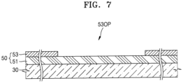
- FIG. 7 is a schematic cross-sectional view of the display panel 30 and the cover panel 50.
- the cover panel 50 may include a cushion layer 51 and a metal layer 53.
- the cushion layer 51 may be attached to the display panel 30 through an adhesive.
- the metal layer 53 may include, for example, copper.
- the cover panel 50 may be disposed over a side of the display panel 30 to face away from the window 10 (i.e., may be disposed in the +z direction from the display panel 30) to shield the display panel 30 from external electrical signals or electromagnetic waves.
- the metal layer 53 of the cover panel 50 may have a transmissive opening 53OP.
- sensitivity of the near-field communication antenna ATN may be degraded.
- the metal layer 53 of the cover panel 50 may have the transmissive opening 53OP, and thus, the degradation of sensitivity of the near-field communication antenna ATN may be effectively prevented.
- the transmissive opening 53OP in the metal layer 53 may overlap the antenna area 41a of the printed circuit board 40, and thus, high sensitivity of the near-field communication antenna ATN may be maintained.
- an area of the transmissive opening 53OP of the metal layer 53 may be substantially equal to or greater than that of the antenna area 41a of the printed circuit board 40, and thus, high sensitivity of the near-field communication antenna ATN may be reliably maintained.
- the electronic apparatus is a smartwatch or smartphone
- a user may place the display panel 30 and the window 10 adjacent to a near-field communication device. Accordingly, electromagnetic waves from the near-field communication device may pass through the window 10, the display panel 30, and the cover panel 50 and reach the near-field communication antenna ATN of the printed circuit board 40.
- the metal layer 53 included in the cover panel 50 may have the transmissive opening 53OP, and accordingly, even in case that a user uses the electronic apparatus in such a way, near-field communication may be performed smoothly.
- An electrical signal received or generated by the near-field communication antenna ATN may be transmitted to the main circuit board 60.
- the first connector 40c1 may be disposed on the printed circuit board 40, the first connector 40c1 may be electrically connected to at least one of the wires of the printed circuit board 40 and the near-field communication antenna ATN. Accordingly, the electrical signal received or generated by the near-field communication antenna ATN may be transmitted to the main circuit board 60 through the first connector 40c1 of the printed circuit board 40 and the first main connector 60c 1 of the main circuit board 60.
- FIG. 8 is a schematic plan view of a portion of the printed circuit board 40 of the electronic apparatus of FIG. 1 .
- FIG. 9 is a schematic cross-sectional view of the portion of the printed circuit board 40 of FIG. 8 , taken along a line B-B' of FIG. 8 .
- the near-field communication antenna ATN included in the electronic apparatus according to the embodiment may include a first antenna ATN1 and a second antenna ATN2. Because the first antenna ATN1 may correspond to the near-field communication antenna ATN described above with reference to FIG. 5 , the second antenna ATN2 may be referred to as an additional antenna from this perspective.
- the near-field communication antenna ATN includes the first antenna ATN1 and the second antenna ATN2.
- the near-field communication antenna ATN may be arranged in the form of a coil in a plane (e.g., the x-y plane) where the printed circuit board 40 is disposed.
- the first antenna ATN1 is illustrated as having a shape like a wire extending from the outside to the inside while rotating clockwise.
- the second antenna ATN2 is illustrated as having a shape like a wire extending from the inside to the outside while rotating counterclockwise.
- embodiments are not limited thereto, and the first antenna ATN1 and the second antenna ATN2 may have different shapes within the scope of the disclosure.
- the first terminal ATNT1 may be electrically connected to an end of the first antenna ATN1.
- An end of the second antenna ATN2 may be electrically connected to another end of the first antenna ATN 1.
- the second terminal ATNT2 may be electrically connected to another end of the second antenna ATN2.
- an induced current corresponding to an hourly change in magnetic flux density passing through the near-field communication antenna ATN may be induced in the near-field communication antenna ATN.
- the near-field communication antenna ATN may include the second antenna ATN2 in addition to the first antenna ATN1, thereby reacting to such a change in magnetic flux density more sensitively.
- the first terminal ATNT1 and the first antenna ATN1 may be on a same layer.
- the first terminal ATNT1 and the first antenna ATN1 may be disposed between the first base B1 and the second base B2.
- the first terminal ATNT1 and the first antenna ATN1 may be integrally formed as a single body.
- the second antenna ATN2 may be between the second base B2 and the third base B3, and an end thereof may be in contact with another end of the first antenna ATN1 through a contact hole defined in the second base B2.
- the second terminal ATNT2 and the first terminal ATNT1 may be on a same layer. Accordingly, another end of the second antenna ATN2 may be in contact with the second terminal ATNT2 through a contact hole defined in the second base B2.
- an electrical signal received or generated by the near-field communication antenna ATN may be transmitted to the main circuit board 60 through the first connector 40c1 of the printed circuit board 40 and the first main connector 60c 1 of the main circuit board 60.
- the printed circuit board 40 may include the first connector 40c1 and a second connector 40c2
- the main circuit board 60 may include the first main connector 60c1 and a second main connector 60c2.
- the printed circuit board 40 may include a second connecting portion 47 protruding from the body portion 41 in addition to the first connecting portion 45 protruding from the body portion 41, the first connector 40c1 may be on the first connecting portion 45, and the second connector 40c2 may be on the second connecting portion 47.
- the first connector 40c1 of the printed circuit board 40 may be electrically connected to at least one of the wires of the printed circuit board 40, and the second connector 40c2 may be connected to wires electrically connected to the near-field communication antenna ATN.
- the first main connector 60c 1 of the main circuit board 60 may be electrically connected to the first connector 40c 1
- the second main connector 60c2 of the main circuit board 60 may be electrically connected to the second connector 40c2.
- an electrical signal to be applied to the display panel 30 may be transmitted to the display panel 30 through the first main connector 60c1 and the first connector 40c1, and an electrical signal from the near-field communication antenna ATN or an electrical signal to the near-field communication antenna ATN may be transmitted through the second main connector 60c2 and the second connector 40c2.
- the main circuit board 60 may include the near-field communication antenna ATN.
- FIG. 12 is an exploded perspective view schematically showing a portion of an electronic apparatus according to an embodiment.
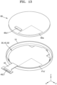
- FIG. 13 is a perspective view schematically showing some elements shown in FIG. 12 which are stacked on each other or bent and shows a case where the main circuit board 60 has an antenna area 60a.
- the printed circuit board 40 may have a transmissive area 41a' corresponding to the antenna area 60a of the main circuit board 60.
- a description of the electronic apparatus according to the previous embodiment may also apply to the electronic apparatus according to the embodiment, except for the antenna area 60a and the transmissive area 41a'.
- the main circuit board 60 may have the antenna area 60a and a peripheral area outside the antenna area 60a, and the near-field communication antenna ATN may be in the antenna area 60a.
- an induced current corresponding to an hourly change in magnetic flux density passing through the near-field communication antenna ATN may be induced in the near-field communication antenna ATN.
- the near-field communication antenna ATN may be arranged in the form of a coil in a plane (e.g., the x-y plane) where the main circuit board 60 is disposed.
- a first terminal may be electrically connected to an end of the near-field communication antenna ATN, and a second terminal may be electrically connected to another end of the near-field communication antenna ATN.
- Each of the first terminal and the second terminal may be, for example, a portion of a wire.
- the first terminal may be disposed on a layer on which the near-field communication antenna ATN may be disposed and thus the first terminal and the near-field communication antenna ATN may be integrally formed as a single body, and the second terminal may be on a layer different from the layer on which the near-field communication antenna ATN may be disposed and may be in contact with the near-field communication antenna ATN through a contact hole.
- the main circuit board 60 may have a structure in which one or more insulating layers may be sequentially stacked on one another, and the near-field communication antenna ATN and the first terminal may be disposed between a first insulating layer and a second insulating layer, and the second terminal may be disposed between the second insulating layer and a third insulating layer and may be in contact with another end of the near-field communication antenna ATN through a contact hole defined in the second insulating layer.
- the main circuit board 60 may have a cross-sectional shape similar to that of the printed circuit board 40 shown in FIG. 6 .
- the main circuit board 60 may include the near-field communication antenna ATN, and accordingly, an electronic apparatus capable of near-field communication and having a simple structure compared to a case where the near-field communication antenna ATN is provided as a separate element distinct from the main circuit board 60 may be implemented.
- wires may be arranged at the main circuit board 60 to transmit an electrical signal to be applied to the printed circuit board 40 through those wires.
- the near-field communication antenna ATN may be in the antenna area 60a.
- wires connected to the near-field communication antenna ATN for example, except the first terminal and the second terminal, other wires may not be in the antenna area 60a but in the peripheral area.
- the cover panel 50 may be disposed between the display panel 30 and the printed circuit board 40. Even in this case, the cover panel 50 may have a structure as shown in FIG. 7 .
- the cover panel 50 may include the cushion layer 51 and the metal layer 53.
- the cushion layer 51 may be attached to the display panel 30 through an adhesive.
- the metal layer 53 may include, for example, copper.
- the cover panel 50 may be disposed over a side of the display panel 30 to face away from the window 10 (i.e., may be disposed in +z direction from the display panel 30) to shield the display panel 30 from external electrical signals or electromagnetic waves.
- the metal layer 53 of the cover panel 50 may have the transmissive opening 53OP.
- sensitivity of the near-field communication antenna ATN may be degraded.
- the metal layer 53 of the cover panel 50 may have the transmissive opening 53OP, and thus, the degradation of sensitivity of the near-field communication antenna ATN may be effectively prevented.
- the transmissive opening 53OP in the metal layer 53 may overlap the antenna area 60a of the main circuit board 60, and thus, high sensitivity of the near-field communication antenna ATN may be maintained.
- an area of the transmissive opening 53OP of the metal layer 53 may be substantially equal to or greater than that of the antenna area 60a of the main circuit board 60, and thus, high sensitivity of the near-field communication antenna ATN may be reliably maintained.
- wires included in the printed circuit board 40 may overlap the peripheral area outside the antenna area 60a of the main circuit board 60.
- the transmissive area 41a' of the printed circuit board 40 may overlap the antenna area 60a of the main circuit board 60, thereby maintaining high sensitivity of the near-field communication antenna ATN.
- an area of the transmissive area 41a' of the printed circuit board 40 may be substantially equal to or greater than that of the antenna area 60a of the main circuit board 60, and thus, high sensitivity of the near-field communication antenna ATN may be reliably maintained.
- the near-field communication antenna ATN may have the structure shown in FIGS. 8 and 9 .
- a description of the structure of the near-field communication antenna ATN including the first antenna ATN1 and the second antenna ATN2, described above with reference to FIGS. 8 and 9 may also apply to a case where not the printed circuit board 40 but the main circuit board 60 includes the near-field communication antenna ATN.
- the first antenna ATN1 may have a shape like a wire extending from the outside to the inside while rotating clockwise
- the second antenna ATN2 may have a shape like a wire extending from the inside to the outside while rotating counterclockwise.
- the first terminal ATNT 1 may be electrically connected to an end of the first antenna ATN1
- an end of the second antenna ATN2 may be electrically connected to another end of the first antenna ATN1
- the second terminal ATNT2 may be electrically connected to another end of the second antenna ATN2.
- the first terminal ATNT1 and the first antenna ATN1 may be on a same layer, and the first terminal ATNT1 and the first antenna ATN1 may be integrally formed as a single body.
- the second antenna ATN2 may be disposed on a layer different from the layer on which the first antenna ATN1 may be disposed, and an end thereof may be in contact with another end of the first antenna ATN1 through a contact hole.
- the second terminal ATNT2 and the first terminal ATNT 1 may be on a same layer. Accordingly, another end of the second antenna ATN2 may be in contact with the second terminal ATNT2 through a contact hole.
- an electrical signal from the near-field communication antenna ATN or an electrical signal to the near-field communication antenna ATN may be transmitted to or from a central processing unit, etc., mounted on the main circuit board 60 through wires of the main circuit board 60.
- an electronic apparatus having a simple structure and capable of near-field communication may be implemented.
- one or more embodiments are not limited by such an effect.
Landscapes
- Engineering & Computer Science (AREA)
- Microelectronics & Electronic Packaging (AREA)
- Physics & Mathematics (AREA)
- General Physics & Mathematics (AREA)
- Computer Networks & Wireless Communication (AREA)
- Signal Processing (AREA)
- Telephone Set Structure (AREA)
- Details Of Aerials (AREA)
- Support Of Aerials (AREA)
- Electric Clocks (AREA)
- Transceivers (AREA)
Abstract
Description
- One or more embodiments relate to an electronic apparatus, and more particularly, to an electronic apparatus having a simple structure and capable of near-field communication.
- In general, an electronic apparatus such as a smartwatch or a smartphone includes a display panel. The electronic apparatus also includes a wireless communication antenna to communicate wirelessly with external devices. Particularly, in recent years, an increasing number of electronic apparatuses include an antenna for near-field communication. In addition, the electronic apparatus includes a flexible printed circuit board for generating or transmitting electrical signals to be applied to the display panel. These various configurations of the electronic apparatus are placed in a case that forms the overall appearance of the electronic apparatus.
- However, an electronic apparatus of the related art is complex to manufacture due to the presence of various elements.
- To solve various problems including the above problem, one or more embodiments include an electronic apparatus having a simplified or streamlined structure and capable of near-field communication. However, such a technical problem is an example, and one or more embodiments are not limited thereto.
- Additional aspects will be set forth in part in the description which follows and, in part, will be apparent from the description, or may be learned by practice of the presented embodiments of the disclosure.
- According to one or more embodiments, an electronic apparatus includes a light-transmitting window, a display panel disposed over the light-transmitting window, a printed circuit board electrically connected to the display panel, disposed over a side of the display panel to face away from the light-transmitting window, and including wires and a near-field communication antenna, and a main circuit board electrically connected to the printed circuit board and disposed over a side of the printed circuit board to face away from the display panel.
- The printed circuit board may include an antenna area and a peripheral area outside the antenna area, and the near-field communication antenna may be disposed in the antenna area.
- In the printed circuit board, the wires may not be disposed in the antenna area except for one or more of the wires electrically connected to the near-field communication antenna.
- Among the wires in the printed circuit board, wires other than one or more of the wires electrically connected to the near-field communication antenna may be in the peripheral area.
- The electronic apparatus may further include a cover panel between the display panel and the printed circuit board.
- The cover panel may include a cushion layer and a metal layer, and the metal layer may include a transmissive opening.
- When viewed in a direction perpendicular to the display panel, the transmissive opening may overlap the antenna area.
- When viewed in the direction perpendicular to the display panel, an area of the transmissive opening may be substantially equal to or greater than an area of the antenna area.
- The printed circuit board may include a first connector electrically connected to at least one of the wires and the near-field communication antenna, and the main circuit board may include a first main connector electrically connected to the first connector.
- The printed circuit board may include a first connector electrically connected to at least one of the wires and a second connector electrically connected to the near-field communication antenna, and the main circuit board may include a first main connector electrically connected to the first connector and a second main connector electrically connected to the second connector.
- The electronic apparatus may further include a first terminal electrically connected to an end of the near-field communication antenna, the first terminal and the near-field communication antenna being disposed on a same layer, and a second terminal electrically connected to another end of the near-field communication antenna, the second terminal and the near-field communication antenna being disposed on different layers.
- The first terminal and the near-field communication antenna may be integral with each other.
- The electronic apparatus may further include a first terminal disposed on a layer electrically connected to an end of the near-field communication antenna, the first terminal and the near-field communication antenna being disposed on a same layer, an additional antenna having an end electrically connected to another end of the near-field communication antenna, the additional antenna and the near-field communication antenna being disposed on different layers, and a second terminal electrically connected to another end of the additional antenna.
- The first terminal and the near-field communication antenna may be integral with each other.
- The second terminal and the first terminal may be disposed on a same layer.
- According to one or more embodiments, an electronic apparatus includes a light-transmitting window, a display panel disposed over the light-transmitting window, a printed circuit board electrically connected to the display panel, disposed over a side of the display panel to face away from the light-transmitting window, and including wires that transmit an electrical signal to be applied to the display panel, and a main circuit board electrically connected to the printed circuit board, disposed over a side of the printed circuit board to face away from the display panel, and including wires and a near-field communication antenna.
- The main circuit board may include an antenna area and a peripheral area outside the antenna area, and the near-field communication antenna may be disposed in the antenna area.
- In the main circuit board, the wires may not be disposed in the antenna area except for one or more of the wires electrically connected to the near-field communication antenna.
- Among the wires in the main circuit board, wires other than one or more of the wires electrically connected to the near-field communication antenna may be in the peripheral area.
- The electronic apparatus may further include a cover panel between the display panel and the printed circuit board and including a cushion layer and a metal layer, wherein the metal layer may include a transmissive opening.
- When viewed in a direction perpendicular to the display panel, the transmissive opening may overlap the antenna area, and the wires in the printed circuit board may overlap the peripheral area.
- When viewed in the direction perpendicular to the display panel, an area of the transmissive opening may be substantially equal to or greater than an area of the antenna area.
- At least some of the above and other features of the invention are set out in the claims.
- The above and other aspects, features, and advantages of certain embodiments of the disclosure will be more apparent from the following description taken in conjunction with the accompanying drawings, in which:
-
FIG. 1 is a schematic exploded perspective view of a portion of an electronic apparatus according to an embodiment; -
FIG. 2 is a perspective view schematically showing some elements shown inFIG. 1 which are stacked on each other; -
FIG. 3 is a perspective view schematically showing some elements shown inFIG. 2 which are bent; -
FIG. 4 is a perspective view schematically showing a shape of a portion of the electronic apparatus ofFIG. 1 during a process of manufacturing the electronic apparatus ofFIG. 1 ; -
FIG. 5 is a schematic plan view of a printed circuit board of the electronic apparatus ofFIG. 1 ; -
FIG. 6 is a schematic cross-sectional view of the printed circuit board ofFIG. 5 , taken along line A-A' ofFIG. 5 ; -
FIG. 7 is a schematic cross-sectional view of a cover panel included in the electronic apparatus ofFIG. 1 ; -
FIG. 8 is a schematic plan view of a portion of the printed circuit board of the electronic apparatus ofFIG. 1 ; -
FIG. 9 is a schematic cross-sectional view of the portion of the printed circuit board ofFIG. 8 , taken along line B-B' ofFIG. 8 ; -
FIG. 10 is an exploded perspective view schematically showing a portion of an electronic apparatus according to an embodiment; -
FIG. 11 is a perspective view schematically showing some elements shown inFIG. 10 being stacked on each other and some elements being bent; -
FIG. 12 is an exploded perspective view schematically showing a portion of an electronic apparatus according to an embodiment; and -
FIG. 13 is a perspective view schematically showing some elements shown inFIG. 12 which are stacked on each other or bent. - Reference will now be made in detail to embodiments, examples of which are illustrated in the accompanying drawings. In this regard, the embodiments may have different forms and should not be construed as being limited to the descriptions set forth herein. Accordingly, the embodiments are merely described below, by referring to the figures, to explain aspects of the description.
- The term "and/or" includes all combinations of one or more of which associated configurations may define. For example, "A and/or B" may be understood to mean "A, B, or A and B."
- For the purposes of this disclosure, the phrase "at least one of A and B" may be construed as A only, B only, or any combination of A and B. Also, "at least one of X, Y, and Z" and "at least one selected from the group consisting of X, Y, and Z" may be construed as X only, Y only, Z only, or any combination of two or more of X, Y, and Z.
- As the description allows for various changes and numerous embodiments, certain embodiments will be illustrated in the drawings and described in the written description. Effects and features of one or more embodiments and methods of accomplishing the same will become apparent from the following detailed description of the one or more embodiments, taken in conjunction with the accompanying drawings. However, the embodiments may have different forms and should not be construed as being limited to the descriptions set forth herein.
- One or more embodiments will be described below in more detail with reference to the accompanying drawings. Those elements that are the same or are in correspondence with each other are rendered the same reference numeral or character regardless of the figure number, and redundant descriptions thereof may be omitted.
- It will be understood that, when an element, such as a layer, a film, a region, or a plate, is referred to as being "on" another element, it may be "directly on" the other element, or intervening elements may be present therebetween. In addition, sizes of elements in the drawings may be exaggerated or reduced for convenience of explanation. For example, since sizes and thicknesses of elements in the drawings may be arbitrarily illustrated for convenience of explanation, the following embodiments are not limited thereto.
- The x-axis, the y-axis, and the z-axis are not limited to three axes of the rectangular coordinate system and may be interpreted in a broader sense. For example, the x-axis, the y-axis, and the z-axis may be perpendicular to one another or may represent different directions that are not perpendicular to one another.
- While such terms as "first" and "second" may be used to describe various elements, such elements must not be limited to the above terms. The above terms are used only to distinguish one element from another.
- It will be further understood that the terms "include," "comprise," and "have" as used herein specify the presence of stated features or elements but do not preclude the addition of one or more other features or elements.
- It will be further understood that, when layers, regions, or elements are referred to as being connected to each other, they may be directly connected to each other or may be indirectly connected to each other with intervening layers, regions, or elements therebetween. For example, when layers, regions, or elements are referred to as being electrically connected to each other, they may be directly electrically connected to each other or may be indirectly electrically connected to each other with intervening layers, regions, or elements therebetween.
- Unless otherwise defined or implied herein, all terms (including technical and scientific terms) used herein have the same meaning as commonly understood by those skilled in the art to which this disclosure pertains. It will be further understood that terms, such as those defined in commonly used dictionaries, should be interpreted as having a meaning that is consistent with their meaning in the context of the relevant art and the disclosure, and should not be interpreted in an ideal or excessively formal sense unless clearly so defined herein.
-
FIG. 1 is a schematic exploded perspective view of a portion of an electronic apparatus according to an embodiment.FIG. 2 is a perspective view schematically showing some elements shown inFIG. 1 which are stacked on each other.FIG. 3 is a perspective view schematically showing some elements shown inFIG. 2 which are bent. - The electronic apparatus according to the embodiment may include a
window 10, adisplay panel 30, a printedcircuit board 40, and/or amain circuit board 60. In some cases, the electronic apparatus may further include various elements as shown inFIG. 1 . For example, the electronic apparatus may further include acover panel 50 disposed between thedisplay panel 30 and the printedcircuit board 40. The electronic apparatus may further include a back cover (not shown) coupled to thewindow 10 to allow various elements to be positioned inside. - Examples of the electronic apparatus may include various electronics such as a smartwatch, a smartphone, and/or a tablet.
- The
window 10 may be formed of a light-transmitting material and may include glass or polymer resin. Thewindow 10 may include, for example, polymer resin such as polyethersulfone, polyacrylate, polyetherimide, polyethylene naphthalate, polyethylene terephthalate, polyphenylene sulfide, polyarylate, polyimide, polycarbonate, or cellulose acetate propionate. - The
window 10 may include abase 11 and anedge portion 13. The base 11 may determine the overall appearance of thewindow 10 and transmit light. Theedge portion 13 may protrude from a first virtual plane on (or in) which thebase 11 is located.FIG. 1 shows that the base 11 may be located on the first virtual plane that is approximately parallel to an x-y plane and theedge portion 13 may protrude from an edge of the base 11 approximately in a direction (e.g., +z direction) perpendicular to the x-y plane. Thebase 11 and theedge portion 13 may include a same material and may be integrally formed as a single body (or integral with each other), but one or more embodiments are not limited thereto. For example, theedge portion 13 may be a separate element from thebase 11 and may be coupled to the edge of thebase 11. In this case, theedge portion 13 may be non-transmissive, unlike the light-transmittingbase 11. - The base 11 may be located in the first virtual plane, and the first plane may be curved. For example, in case that the electronic apparatus is a smartwatch, the base 11 included in the
window 10 may have a flat shape as a whole, but an outer surface of the base 11 opposite to the display panel 30 (i.e., the outer surface in -z direction) may include a portion that is microscopically curved. - The
display panel 30 may be disposed on thebase 11 of thewindow 10. Thedisplay panel 30 may include a circuit that includes an electronic device such as a thin-film transistor on a substrate, and a display element such as an organic or inorganic light-emitting diode electrically connected to the circuit. However, one or more embodiments are not limited thereto, and thedisplay panel 30 may include various display elements such as a liquid crystal device instead of the organic light-emitting diode. - The printed
circuit board 40 may be flexible. The printedcircuit board 40 may be electrically connected to thedisplay panel 30. For example, as shown inFIG. 1 , a portion of the printedcircuit board 40 may be attached onto and/or electrically connected onto a surface of thedisplay panel 30 in a direction toward thewindow 10. In this case, wires or pads of the printedcircuit board 40 may be electrically connected to pads positioned on the surface of thedisplay panel 30 in a direction toward thewindow 10 through an anisotropic conductive film, etc. - The printed
circuit board 40 may include abody portion 41, aneck portion 43 protruding from thebody portion 41, and/or a first connectingportion 45 protruding from thebody portion 41. Theneck portion 43 may be in contact with thedisplay panel 30 as described above. Thebody portion 41 may have an area greater than that of theneck portion 43, and an electronic device such as an integrated circuit may be attached to thebody portion 41 of the printedcircuit board 40 through an anisotropic conductive film, etc. Pads electrically connected to an electronic device may be positioned in thebody portion 41, and wires extending to theneck portion 43 and/or the first connectingportion 45 may also be positioned in thebody portion 41. Electrical signals to be applied to thedisplay panel 30 may be transmitted through the wires. Further, as will be described below, a near-field communication antenna ATN (refer toFIG. 5 ) may be positioned at thebody portion 41. A first connector 40c1 may be positioned at the first connectingportion 45, and wires extending from thebody portion 41 may be electrically connected to thefirst connector 40c 1. - The
cover panel 50 may be disposed between thedisplay panel 30 and the printedcircuit board 40. A detailed description of thecover panel 50 is given below. - The
display panel 30 and thecover panel 50 may be on thewindow 10 as shown inFIG. 2 . For example, thedisplay panel 30 and thecover panel 50 may be positioned inside a space defined by thebase 11 and theedge portion 13 of thewindow 10. The printedcircuit board 40 electrically connected to thedisplay panel 30 may be bent at theneck portion 43 as shown inFIG. 3 , and thus, thebody portion 41 may be placed on thecover panel 50. The printedcircuit board 40 may be flexible as described above, theneck portion 43 may be flexible and may be bent as shown inFIGS. 2 and3 , and thebody portion 41 may be placed on thecover panel 50. In some cases, thebody portion 41 may also be flexible. In this case, theneck portion 43 may be more flexible than thebody portion 41. - The printed
circuit board 40 having theneck portion 43 electrically connected to thedisplay panel 30 as described above may be bent at theneck portion 43, and thebody portion 41 may be disposed over a side of thedisplay panel 30 to face away from the window 10 (e.g., may be disposed in the +z direction from the display panel 30). It may be understood as describing that the printedcircuit board 40 is opposite to the window 10 (in the +z direction) with respect to thedisplay panel 30. - As shown in
FIG. 3 , themain circuit board 60 may be on the printedcircuit board 40 having theneck portion 43 bent. Themain circuit board 60 may be electrically connected to the printedcircuit board 40 and may be disposed over a side of the printedcircuit board 40 to face away from the display panel 30 (e.g., may be disposed in the +z direction from the printed circuit board 40). Electronic elements such as an application processor (AP) or a central processing unit (CPU) of an electronic apparatus may be on themain circuit board 60, and wires configured to transmit an electrical signal from those electronic elements or an electrical signal to those electronic elements may also be on themain circuit board 60. Themain circuit board 60 may not be flexible unlike the printedcircuit board 40. Themain circuit board 60 may include a first main connector 60c1, and the first connector 40c1 of the printedcircuit board 40 may be fastened to the firstmain connector 60c 1 of themain circuit board 60 to electrically connect the printedcircuit board 40 to themain circuit board 60. -
FIG. 4 is a perspective view schematically showing a shape of a portion of the electronic apparatus ofFIG. 1 during a process of manufacturing the electronic apparatus ofFIG. 1 . As shown inFIG. 4 , during a process of manufacturing the electronic apparatus, thedisplay panel 30 and thecover panel 50 are placed in a space defined by thebase 11 and theedge portion 13 of thewindow 10, and then, the printedcircuit board 40 is bent at theneck portion 43 to place thebody portion 41 of the printedcircuit board 40 on thedisplay panel 30 and thecover panel 50.FIG. 4 may be understood as showing a process of placing thedisplay panel 30 and thecover panel 50 in a space defined by thebase 11 and theedge portion 13 of thewindow 10 during a process of manufacturing the electronic apparatus. A light-transmittingadhesive layer 20 may be disposed between thewindow 10 and thedisplay panel 30 to bond thewindow 10 and thedisplay panel 30. -
FIG. 5 is a schematic plan view of the printedcircuit board 40 of the electronic apparatus ofFIG. 1 .FIG. 6 is a schematic cross-sectional view of the printedcircuit board 40 ofFIG. 5 , taken along a line A-A' ofFIG. 5 . As described above, the printedcircuit board 40 includes the near-field communication antenna ATN. The printedcircuit board 40 may have anantenna area 41a and a peripheral area outside theantenna area 41a. The near-field communication antenna ATN may be in theantenna area 41a. As shown inFIG. 5 , theantenna area 41a may be positioned at thebody portion 41 of the printedcircuit board 40. - An induced current corresponding to an hourly change in magnetic flux density passing through the near-field communication antenna ATN may be induced in the near-field communication antenna ATN. To react to such a change in magnetic flux density sensitively, as shown in
FIG. 5 , the near-field communication antenna ATN may be arranged in a form of a coil in a plane (e.g., the x-y plane) where the printedcircuit board 40 is disposed. InFIG. 5 , the near-field communication antenna ATN is illustrated as having a shape like a wire extending from the outside to the inside while rotating clockwise. However, embodiments are not limited thereto, and the near-field communication antenna ATN may have different shapes within the scope of the disclosure. - A first terminal ATNT1 may be electrically connected to an end of the near-field communication antenna ATN, and a second terminal ATNT2 may be electrically connected to another end of the near-field communication antenna ATN. Each of the first terminal ATNT1 and the second terminal ATNT2 may be, for example, a portion of a wire.
FIGS. 5 and6 show that the first terminal ATNT1 may be disposed on a layer on which the near-field communication antenna ATN may be disposed such that the first terminal ATNT1 and the near-field communication antenna ATN are integrally formed as a single body, and the second terminal ATNT2 may be disposed on a layer different from the layer on which the near-field communication antenna ATN may be disposed. For example, the printedcircuit board 40 may have a structure in which a first base B1, a second base B2, and a third base B3, which are insulating layers including a resin (e.g., polyimide or a similar resin), are sequentially stacked on one another, and the near-field communication antenna ATN and the first terminal ATNT1 may be disposed between the first base B1 and the second base B2, and the second terminal ATNT2 may be disposed between the second base B2 and the third base B3 and may be in contact with the another end of the near-field communication antenna ATN through a contact hole defined in the second base B2. - In the above case of the electronic apparatus according to the embodiment, the printed
circuit board 40 may include the near-field communication antenna ATN, and accordingly, an electronic apparatus capable of near-field communication and having a simple structure compared to a case where the near-field communication antenna ATN is provided as a separate element distinct from the printedcircuit board 40 may be implemented. - As described above, wires may be arranged at the printed
circuit board 40 to transmit an electrical signal to be applied to thedisplay panel 30 etc. through those wires. The wires may be omitted inFIG. 5 for convenience of illustration. As described above, the near-field communication antenna ATN may be in theantenna area 41a. On the other hand, except wires connected to the near-field communication antenna ATN, for example, except the first terminal ATNT1 and the second terminal ATNT2, other wires may not be in theantenna area 41a but in the peripheral area. For example, in the printedcircuit board 40, there may be no wires in theantenna area 41a, other than a wire or wires connected to the near-field communication antenna ATN. - As described above, because an induced current corresponding to an hourly change in magnetic flux density passing through the near-field communication antenna ATN may be induced in the near-field communication antenna ATN, the near-field communication antenna ATN may sense an ambient signal. If a wire including metal is in the
antenna area 41a, sensitivity of the near-field communication antenna ATN may be degraded. Accordingly, except wires connected to the near-field communication antenna ATN, for example, except the first terminal ATNT1 and the second terminal ATNT2, other wires may not be in theantenna area 41a but in the peripheral area. For reference, as shown inFIG. 6 , the printedcircuit board 40 may have a multi-layer structure, and the first terminal ATNT1 may be disposed on a layer different from a layer on which the second terminal ATNT2 is disposed. Similarly, some of wires included in the printedcircuit board 40 may be between the first base B1 and the second base B2, and some may be between the second base B2 and the third base B3. In any case, those wires may not be in theantenna area 41a. - As described above, the
cover panel 50 may be disposed between thedisplay panel 30 and the printedcircuit board 40.FIG. 7 is a schematic cross-sectional view of thedisplay panel 30 and thecover panel 50. As shown inFIG. 7 , thecover panel 50 may include acushion layer 51 and ametal layer 53. In some cases, thecushion layer 51 may be attached to thedisplay panel 30 through an adhesive. Themetal layer 53 may include, for example, copper. Thecover panel 50 may be disposed over a side of thedisplay panel 30 to face away from the window 10 (i.e., may be disposed in the +z direction from the display panel 30) to shield thedisplay panel 30 from external electrical signals or electromagnetic waves. - As shown in
FIG. 7 , themetal layer 53 of thecover panel 50 may have a transmissive opening 53OP. As described above, in case that a wire including metal is in theantenna area 41a, sensitivity of the near-field communication antenna ATN may be degraded. Even in case that themetal layer 53 of thecover panel 50 overlaps theantenna area 41a, sensitivity of the near-field communication antenna ATN may be degraded. Accordingly, themetal layer 53 of thecover panel 50 may have the transmissive opening 53OP, and thus, the degradation of sensitivity of the near-field communication antenna ATN may be effectively prevented. Particularly, when viewed in a direction (the z-axis direction) perpendicular to the display panel 30 (i.e., in a plan view), the transmissive opening 53OP in themetal layer 53 may overlap theantenna area 41a of the printedcircuit board 40, and thus, high sensitivity of the near-field communication antenna ATN may be maintained. In this regard, when viewed in the direction (the z-axis direction) perpendicular to thedisplay panel 30, an area of the transmissive opening 53OP of themetal layer 53 may be substantially equal to or greater than that of theantenna area 41a of the printedcircuit board 40, and thus, high sensitivity of the near-field communication antenna ATN may be reliably maintained. - For reference, in case that the electronic apparatus according to the embodiment is a smartwatch or smartphone, a user may place the
display panel 30 and thewindow 10 adjacent to a near-field communication device. Accordingly, electromagnetic waves from the near-field communication device may pass through thewindow 10, thedisplay panel 30, and thecover panel 50 and reach the near-field communication antenna ATN of the printedcircuit board 40. In the electronic apparatus according to the embodiment, themetal layer 53 included in thecover panel 50 may have the transmissive opening 53OP, and accordingly, even in case that a user uses the electronic apparatus in such a way, near-field communication may be performed smoothly. - An electrical signal received or generated by the near-field communication antenna ATN may be transmitted to the
main circuit board 60. As described above, because the first connector 40c1 may be disposed on the printedcircuit board 40, the first connector 40c1 may be electrically connected to at least one of the wires of the printedcircuit board 40 and the near-field communication antenna ATN. Accordingly, the electrical signal received or generated by the near-field communication antenna ATN may be transmitted to themain circuit board 60 through the first connector 40c1 of the printedcircuit board 40 and the firstmain connector 60c 1 of themain circuit board 60. -
FIG. 8 is a schematic plan view of a portion of the printedcircuit board 40 of the electronic apparatus ofFIG. 1 .FIG. 9 is a schematic cross-sectional view of the portion of the printedcircuit board 40 ofFIG. 8 , taken along a line B-B' ofFIG. 8 . As shown inFIG. 8 , the near-field communication antenna ATN included in the electronic apparatus according to the embodiment may include a first antenna ATN1 and a second antenna ATN2. Because the first antenna ATN1 may correspond to the near-field communication antenna ATN described above with reference toFIG. 5 , the second antenna ATN2 may be referred to as an additional antenna from this perspective. Hereinafter, it is assumed for convenience of description that the near-field communication antenna ATN includes the first antenna ATN1 and the second antenna ATN2. - As shown in
FIG. 8 , the near-field communication antenna ATN may be arranged in the form of a coil in a plane (e.g., the x-y plane) where the printedcircuit board 40 is disposed. InFIG. 8 , the first antenna ATN1 is illustrated as having a shape like a wire extending from the outside to the inside while rotating clockwise. The second antenna ATN2 is illustrated as having a shape like a wire extending from the inside to the outside while rotating counterclockwise. However, embodiments are not limited thereto, and the first antenna ATN1 and the second antenna ATN2 may have different shapes within the scope of the disclosure. - The first terminal ATNT1 may be electrically connected to an end of the first antenna ATN1. An end of the second antenna ATN2 may be electrically connected to another end of the
first antenna ATN 1. The second terminal ATNT2 may be electrically connected to another end of the second antenna ATN2. As described above, an induced current corresponding to an hourly change in magnetic flux density passing through the near-field communication antenna ATN may be induced in the near-field communication antenna ATN. The near-field communication antenna ATN may include the second antenna ATN2 in addition to the first antenna ATN1, thereby reacting to such a change in magnetic flux density more sensitively. - The first terminal ATNT1 and the first antenna ATN1 may be on a same layer. For example, the first terminal ATNT1 and the first antenna ATN1 may be disposed between the first base B1 and the second base B2. Accordingly, the first terminal ATNT1 and the first antenna ATN1 may be integrally formed as a single body. The second antenna ATN2 may be between the second base B2 and the third base B3, and an end thereof may be in contact with another end of the first antenna ATN1 through a contact hole defined in the second base B2. The second terminal ATNT2 and the first terminal ATNT1 may be on a same layer. Accordingly, another end of the second antenna ATN2 may be in contact with the second terminal ATNT2 through a contact hole defined in the second base B2.
- It has been described thus far that an electrical signal received or generated by the near-field communication antenna ATN may be transmitted to the
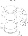
main circuit board 60 through the first connector 40c1 of the printedcircuit board 40 and the firstmain connector 60c 1 of themain circuit board 60. However, one or more embodiments are not limited thereto. For example, as shown inFIG. 10 , which is an exploded perspective view schematically showing a portion of an electronic apparatus according to an embodiment, andFIG. 11 , which is a perspective view schematically showing some elements shown inFIG. 10 being stacked on each other and some elements being bent, the printedcircuit board 40 may include the first connector 40c1 and a second connector 40c2, and themain circuit board 60 may include the first main connector 60c1 and a second main connector 60c2. - For example, the printed
circuit board 40 may include a second connectingportion 47 protruding from thebody portion 41 in addition to the first connectingportion 45 protruding from thebody portion 41, the first connector 40c1 may be on the first connectingportion 45, and the second connector 40c2 may be on the second connectingportion 47. - In this case, the first connector 40c1 of the printed
circuit board 40 may be electrically connected to at least one of the wires of the printedcircuit board 40, and the second connector 40c2 may be connected to wires electrically connected to the near-field communication antenna ATN. The firstmain connector 60c 1 of themain circuit board 60 may be electrically connected to thefirst connector 40c 1, and the second main connector 60c2 of themain circuit board 60 may be electrically connected to the second connector 40c2. Thus, an electrical signal to be applied to thedisplay panel 30 may be transmitted to thedisplay panel 30 through the first main connector 60c1 and the first connector 40c1, and an electrical signal from the near-field communication antenna ATN or an electrical signal to the near-field communication antenna ATN may be transmitted through the second main connector 60c2 and the second connector 40c2. - Although a case where the printed
circuit board 40 includes the near-field communication antenna ATN has been described thus far, one or more embodiments are not limited thereto. For example, themain circuit board 60 may include the near-field communication antenna ATN.FIG. 12 is an exploded perspective view schematically showing a portion of an electronic apparatus according to an embodiment.FIG. 13 is a perspective view schematically showing some elements shown inFIG. 12 which are stacked on each other or bent and shows a case where themain circuit board 60 has anantenna area 60a. The printedcircuit board 40 may have atransmissive area 41a' corresponding to theantenna area 60a of themain circuit board 60. A description of the electronic apparatus according to the previous embodiment may also apply to the electronic apparatus according to the embodiment, except for theantenna area 60a and thetransmissive area 41a'. - The
main circuit board 60 may have theantenna area 60a and a peripheral area outside theantenna area 60a, and the near-field communication antenna ATN may be in theantenna area 60a. - An induced current corresponding to an hourly change in magnetic flux density passing through the near-field communication antenna ATN may be induced in the near-field communication antenna ATN. To react to such a change in magnetic flux density sensitively, the near-field communication antenna ATN may be arranged in the form of a coil in a plane (e.g., the x-y plane) where the
main circuit board 60 is disposed. - A first terminal may be electrically connected to an end of the near-field communication antenna ATN, and a second terminal may be electrically connected to another end of the near-field communication antenna ATN. Each of the first terminal and the second terminal may be, for example, a portion of a wire. The first terminal may be disposed on a layer on which the near-field communication antenna ATN may be disposed and thus the first terminal and the near-field communication antenna ATN may be integrally formed as a single body, and the second terminal may be on a layer different from the layer on which the near-field communication antenna ATN may be disposed and may be in contact with the near-field communication antenna ATN through a contact hole. For example, the
main circuit board 60 may have a structure in which one or more insulating layers may be sequentially stacked on one another, and the near-field communication antenna ATN and the first terminal may be disposed between a first insulating layer and a second insulating layer, and the second terminal may be disposed between the second insulating layer and a third insulating layer and may be in contact with another end of the near-field communication antenna ATN through a contact hole defined in the second insulating layer. For example, themain circuit board 60 may have a cross-sectional shape similar to that of the printedcircuit board 40 shown inFIG. 6 . - In the above case of the electronic apparatus according to the embodiment, the
main circuit board 60 may include the near-field communication antenna ATN, and accordingly, an electronic apparatus capable of near-field communication and having a simple structure compared to a case where the near-field communication antenna ATN is provided as a separate element distinct from themain circuit board 60 may be implemented. - As described above, wires may be arranged at the
main circuit board 60 to transmit an electrical signal to be applied to the printedcircuit board 40 through those wires. As described above, the near-field communication antenna ATN may be in theantenna area 60a. On the other hand, except wires connected to the near-field communication antenna ATN, for example, except the first terminal and the second terminal, other wires may not be in theantenna area 60a but in the peripheral area. For example, in themain circuit board 60, there may be no wires in theantenna area 60a, other than a wire or wires connected to the near-field communication antenna ATN. - Even in the electronic apparatus according to the embodiment, the
cover panel 50 may be disposed between thedisplay panel 30 and the printedcircuit board 40. Even in this case, thecover panel 50 may have a structure as shown inFIG. 7 . For example, thecover panel 50 may include thecushion layer 51 and themetal layer 53. In some cases, thecushion layer 51 may be attached to thedisplay panel 30 through an adhesive. Themetal layer 53 may include, for example, copper. Thecover panel 50 may be disposed over a side of thedisplay panel 30 to face away from the window 10 (i.e., may be disposed in +z direction from the display panel 30) to shield thedisplay panel 30 from external electrical signals or electromagnetic waves. - As shown in
FIG. 7 , themetal layer 53 of thecover panel 50 may have the transmissive opening 53OP. As described above, in case that a wire including metal is in theantenna area 60a, sensitivity of the near-field communication antenna ATN may be degraded. Even in case that themetal layer 53 of thecover panel 50 overlaps theantenna area 60a, sensitivity of the near-field communication antenna ATN may be degraded. Accordingly, themetal layer 53 of thecover panel 50 may have the transmissive opening 53OP, and thus, the degradation of sensitivity of the near-field communication antenna ATN may be effectively prevented. Particularly, when viewed in the direction (the z-axis direction) perpendicular to thedisplay panel 30, the transmissive opening 53OP in themetal layer 53 may overlap theantenna area 60a of themain circuit board 60, and thus, high sensitivity of the near-field communication antenna ATN may be maintained. In this regard, when viewed in the direction (the z-axis direction) perpendicular to thedisplay panel 30, an area of the transmissive opening 53OP of themetal layer 53 may be substantially equal to or greater than that of theantenna area 60a of themain circuit board 60, and thus, high sensitivity of the near-field communication antenna ATN may be reliably maintained. - Similarly, when viewed in the direction (the z-axis direction) perpendicular to the
display panel 30, wires included in the printedcircuit board 40 may overlap the peripheral area outside theantenna area 60a of themain circuit board 60. For example, there may be no wires of the printedcircuit board 40 in thetransmissive area 41a' of the printedcircuit board 40, and when viewed in the direction (the z-axis direction) perpendicular to thedisplay panel 30, thetransmissive area 41a' of the printedcircuit board 40 may overlap theantenna area 60a of themain circuit board 60, thereby maintaining high sensitivity of the near-field communication antenna ATN. In this regard, when viewed in the direction (the z-axis direction) perpendicular to thedisplay panel 30, an area of thetransmissive area 41a' of the printedcircuit board 40 may be substantially equal to or greater than that of theantenna area 60a of themain circuit board 60, and thus, high sensitivity of the near-field communication antenna ATN may be reliably maintained. - Even in case that the
main circuit board 60 includes the near-field communication antenna ATN, the near-field communication antenna ATN may have the structure shown inFIGS. 8 and9 . For example, a description of the structure of the near-field communication antenna ATN including the first antenna ATN1 and the second antenna ATN2, described above with reference toFIGS. 8 and9 , may also apply to a case where not the printedcircuit board 40 but themain circuit board 60 includes the near-field communication antenna ATN. - For example, the first antenna ATN1 may have a shape like a wire extending from the outside to the inside while rotating clockwise, and the second antenna ATN2 may have a shape like a wire extending from the inside to the outside while rotating counterclockwise. The
first terminal ATNT 1 may be electrically connected to an end of the first antenna ATN1, an end of the second antenna ATN2 may be electrically connected to another end of the first antenna ATN1, and the second terminal ATNT2 may be electrically connected to another end of the second antenna ATN2. The first terminal ATNT1 and the first antenna ATN1 may be on a same layer, and the first terminal ATNT1 and the first antenna ATN1 may be integrally formed as a single body. The second antenna ATN2 may be disposed on a layer different from the layer on which the first antenna ATN1 may be disposed, and an end thereof may be in contact with another end of the first antenna ATN1 through a contact hole. The second terminal ATNT2 and thefirst terminal ATNT 1 may be on a same layer. Accordingly, another end of the second antenna ATN2 may be in contact with the second terminal ATNT2 through a contact hole. - For reference, in case that the
main circuit board 60 includes the near-field communication antenna ATN as described above, an electrical signal from the near-field communication antenna ATN or an electrical signal to the near-field communication antenna ATN may be transmitted to or from a central processing unit, etc., mounted on themain circuit board 60 through wires of themain circuit board 60. - According to one or more of the above embodiments, an electronic apparatus having a simple structure and capable of near-field communication may be implemented. However, one or more embodiments are not limited by such an effect.
- It should be understood that embodiments described herein should be considered in a descriptive sense only and not for purposes of limitation. Descriptions of features or aspects within each embodiment should typically be considered as available for other similar features or aspects in other embodiments. While one or more embodiments have been described with reference to the figures, it will be understood by those of ordinary skill in the art that various changes in form and details may be made therein without departing from the scope as defined by the following claims.
Claims (15)
- An electronic apparatus comprising:a light-transmitting window;a display panel disposed over the light-transmitting window;a printed circuit board electrically connected to the display panel, disposed over a side of the display panel to face away from the light-transmitting window, and comprising wires and a near-field communication antenna; anda main circuit board electrically connected to the printed circuit board and disposed over a side of the printed circuit board to face away from the display panel.
- The electronic apparatus of claim 1, whereinthe printed circuit board comprises an antenna area and a peripheral area outside the antenna area, andthe near-field communication antenna is disposed in the antenna area.
- The electronic apparatus of claim 2, wherein, in the printed circuit board, the wires are not disposed in the antenna area except for one or more of the wires electrically connected to the near-field communication antenna.
- The electronic apparatus of claim 2 or 3, wherein, among the wires in the printed circuit board, wires other than one or more of the wires electrically connected to the near-field communication antenna are in the peripheral area.
- The electronic apparatus of any preceding claim, further comprising:
a cover panel between the display panel and the printed circuit board. - The electronic apparatus of claim 5, whereinthe cover panel comprises a cushion layer and a metal layer, andthe metal layer comprises a transmissive opening, and optionallywhen viewed in a direction perpendicular to the display panel, the transmissive opening overlaps an antenna area, and optionallywhen viewed in the direction perpendicular to the display panel, an area of the transmissive opening is substantially equal to or greater than an area of the antenna area.
- The electronic apparatus of any preceding claim, whereinthe printed circuit board comprises a first connector electrically connected to at least one of the wires and the near-field communication antenna, andthe main circuit board comprises a first main connector electrically connected to the first connector.
- The electronic apparatus of any one of claims 1 to 6, whereinthe printed circuit board comprises:a first connector electrically connected to at least one of the wires; anda second connector electrically connected to the near-field communication antenna, andthe main circuit board comprises:a first main connector electrically connected to the first connector; anda second main connector electrically connected to the second connector.
- The electronic apparatus of any preceding claim, further comprising:a first terminal electrically connected to an end of the near-field communication antenna, the first terminal and the near-field communication antenna being disposed on a same layer; anda second terminal electrically connected to another end of the near-field communication antenna, the second terminal and the near-field communication antenna being disposed on different layers, and optionallywherein the first terminal and the near-field communication antenna are integral with each other.
- The electronic apparatus of any one of claims 1 to 8, further comprising:a first terminal disposed on a layer electrically connected to an end of the near-field communication antenna, the first terminal and the near-field communication antenna being disposed on a same layer;an additional antenna having an end electrically connected to another end of the near-field communication antenna, the additional antenna and the near-field communication antenna being disposed on different layers; anda second terminal electrically connected to another end of the additional antenna, and optionallywherein the first terminal and the near-field communication antenna are integral with each other, and/orwherein the second terminal and the first terminal are disposed on a same layer.
- An electronic apparatus comprising:a light-transmitting window;a display panel disposed over the light-transmitting window;a printed circuit board electrically connected to the display panel, disposed over a side of the display panel to face away from the light-transmitting window, and comprising wires that are configured to transmit an electrical signal to be applied to the display panel; anda main circuit board electrically connected to the printed circuit board, disposed over a side of the printed circuit board to face away from the display panel, and comprising wires and a near-field communication antenna.
- The electronic apparatus of claim 11, whereinthe main circuit board comprises an antenna area and a peripheral area outside the antenna area, andthe near-field communication antenna is disposed in the antenna area.
- The electronic apparatus of claim 12, wherein, in the main circuit board, the wires are not disposed in the antenna area except for one or more of the wires electrically connected to the near-field communication antenna.
- The electronic apparatus of claim 12 or 13, wherein, among the wires in the main circuit board, wires other than one or more of the wires electrically connected to the near-field communication antenna are in the peripheral area.
- The electronic apparatus of any one of claims 12 to 14, further comprising:a cover panel between the display panel and the printed circuit board and comprising a cushion layer and a metal layer,wherein the metal layer comprises a transmissive opening, and optionallywhen viewed in a direction perpendicular to the display panel, the transmissive opening overlaps the antenna area, and the wires in the printed circuit board overlap the peripheral area, and optionallywhen viewed in the direction perpendicular to the display panel, an area of the transmissive opening is substantially equal to or greater than an area of the antenna area.
Applications Claiming Priority (1)
| Application Number | Priority Date | Filing Date | Title |
|---|---|---|---|
| KR1020230142348A KR20250058841A (en) | 2023-10-23 | 2023-10-23 | Electronic apparatus |
Publications (2)
| Publication Number | Publication Date |
|---|---|
| EP4546656A2 true EP4546656A2 (en) | 2025-04-30 |
| EP4546656A3 EP4546656A3 (en) | 2025-07-02 |
Family
ID=92627392
Family Applications (1)
| Application Number | Title | Priority Date | Filing Date |
|---|---|---|---|
| EP24197233.0A Pending EP4546656A3 (en) | 2023-10-23 | 2024-08-29 | Electronic apparatus |
Country Status (5)
| Country | Link |
|---|---|
| US (1) | US20250132485A1 (en) |
| EP (1) | EP4546656A3 (en) |
| JP (1) | JP2025071807A (en) |
| KR (1) | KR20250058841A (en) |
| CN (1) | CN119890680A (en) |
Family Cites Families (7)
| Publication number | Priority date | Publication date | Assignee | Title |
|---|---|---|---|---|
| US9246214B2 (en) * | 2012-03-08 | 2016-01-26 | Apple Inc. | Electronic device antenna structures with ferrite layers |
| KR101859575B1 (en) * | 2012-03-21 | 2018-05-18 | 삼성전자 주식회사 | Antenna device for near field wireless communication and electric device having the same |
| US9620843B2 (en) * | 2013-01-31 | 2017-04-11 | Hewlett-Packard Development Company, L.P. | Display panel for front-side wireless communication |
| CN205646168U (en) * | 2016-05-30 | 2016-10-12 | 昆山维信诺科技有限公司 | NFC antenna module and terminal equipment |
| JP7271162B2 (en) * | 2018-12-19 | 2023-05-11 | 株式会社ジャパンディスプレイ | Electronics |
| CN110082976B (en) * | 2019-05-14 | 2022-08-02 | 上海天马微电子有限公司 | Display module and display device |
| KR102682559B1 (en) * | 2019-06-26 | 2024-07-08 | 삼성전자주식회사 | Electronic device including antena structure for narrow space |
-
2023
- 2023-10-23 KR KR1020230142348A patent/KR20250058841A/en active Pending
-
2024
- 2024-05-17 US US18/667,257 patent/US20250132485A1/en active Pending
- 2024-08-29 EP EP24197233.0A patent/EP4546656A3/en active Pending
- 2024-10-08 CN CN202411394480.4A patent/CN119890680A/en active Pending
- 2024-10-22 JP JP2024186202A patent/JP2025071807A/en active Pending
Also Published As
| Publication number | Publication date |
|---|---|
| CN119890680A (en) | 2025-04-25 |
| US20250132485A1 (en) | 2025-04-24 |
| KR20250058841A (en) | 2025-05-02 |
| JP2025071807A (en) | 2025-05-08 |
| EP4546656A3 (en) | 2025-07-02 |
Similar Documents
| Publication | Publication Date | Title |
|---|---|---|
| US12100884B2 (en) | Antenna having single non-conductive portion and electronic device including the same | |
| CN111328193B (en) | Flexible printed circuit board, flexible display module and electronic device | |
| JP5682739B2 (en) | Interface and communication device | |
| KR20180079422A (en) | Display device having NFC communication function | |
| US20140328084A1 (en) | Electronic Device and Display Module with Sensing Antenna | |
| US11114392B2 (en) | Wireless communication device | |
| US9991599B2 (en) | Antenna device, electronic apparatus, and method of mounting antenna device | |
| WO2008004359A1 (en) | Antenna coil to be mounted on substrate and antenna device | |
| CN113196674B (en) | Electronic equipment | |
| CN110554526A (en) | Liquid crystal display with built-in antenna coil | |
| CN110941113A (en) | Display device and manufacturing method thereof | |
| US11877384B2 (en) | Flexible circuit board, manufacturing method thereof and display panel | |
| CN116053782A (en) | an electronic device | |
| US20110210929A1 (en) | Touch panel-attached display device and antistatic structure | |
| US12032404B2 (en) | Display device having a display panel including a member for inducing a magnetic field | |
| CN116075045B (en) | Electronic devices | |
| CN109445213A (en) | Display panel and display device | |
| US20250132485A1 (en) | Electronic apparatus | |
| JP2003142875A (en) | Flexible substrate with shield and display device using the same | |
| EP4142049A1 (en) | Antenna apparatus and electronic device | |
| KR20220110397A (en) | Electronic apparatus | |
| US12284759B2 (en) | Display module and display device | |
| US12119547B2 (en) | High reliability portable device | |
| KR102823728B1 (en) | Electronic device including interposer | |
| US11764527B2 (en) | Connector |
Legal Events
| Date | Code | Title | Description |
|---|---|---|---|
| PUAI | Public reference made under article 153(3) epc to a published international application that has entered the european phase |
Free format text: ORIGINAL CODE: 0009012 |
|
| STAA | Information on the status of an ep patent application or granted ep patent |
Free format text: STATUS: THE APPLICATION HAS BEEN PUBLISHED |
|
| AK | Designated contracting states |
Kind code of ref document: A2 Designated state(s): AL AT BE BG CH CY CZ DE DK EE ES FI FR GB GR HR HU IE IS IT LI LT LU LV MC ME MK MT NL NO PL PT RO RS SE SI SK SM TR |
|
| PUAL | Search report despatched |
Free format text: ORIGINAL CODE: 0009013 |
|
| AK | Designated contracting states |
Kind code of ref document: A3 Designated state(s): AL AT BE BG CH CY CZ DE DK EE ES FI FR GB GR HR HU IE IS IT LI LT LU LV MC ME MK MT NL NO PL PT RO RS SE SI SK SM TR |
|
| RIC1 | Information provided on ipc code assigned before grant |
Ipc: G04G 17/02 20060101ALI20250526BHEP Ipc: G04R 60/06 20130101ALI20250526BHEP Ipc: G04R 60/10 20130101ALI20250526BHEP Ipc: H01Q 1/24 20060101ALI20250526BHEP Ipc: H01Q 7/00 20060101ALI20250526BHEP Ipc: H05K 1/02 20060101ALI20250526BHEP Ipc: G04G 17/04 20060101ALI20250526BHEP Ipc: H01Q 1/27 20060101ALI20250526BHEP Ipc: H04B 5/43 20240101ALI20250526BHEP Ipc: H01Q 1/22 20060101ALI20250526BHEP Ipc: H04B 5/26 20240101AFI20250526BHEP |
|
| STAA | Information on the status of an ep patent application or granted ep patent |
Free format text: STATUS: REQUEST FOR EXAMINATION WAS MADE |
|
| 17P | Request for examination filed |
Effective date: 20260102 |
|
| P01 | Opt-out of the competence of the unified patent court (upc) registered |
Free format text: CASE NUMBER: UPC_APP_0007454_4546656/2026 Effective date: 20260226 |