EP4546501A1 - Protection circuit module and battery pack including the same - Google Patents
Protection circuit module and battery pack including the same Download PDFInfo
- Publication number
- EP4546501A1 EP4546501A1 EP24160413.1A EP24160413A EP4546501A1 EP 4546501 A1 EP4546501 A1 EP 4546501A1 EP 24160413 A EP24160413 A EP 24160413A EP 4546501 A1 EP4546501 A1 EP 4546501A1
- Authority
- EP
- European Patent Office
- Prior art keywords
- disposed
- circuit module
- electrically connected
- protection circuit
- substrate
- Prior art date
- Legal status (The legal status is an assumption and is not a legal conclusion. Google has not performed a legal analysis and makes no representation as to the accuracy of the status listed.)
- Pending
Links
Images



Classifications
-
- H—ELECTRICITY
- H02—GENERATION; CONVERSION OR DISTRIBUTION OF ELECTRIC POWER
- H02H—EMERGENCY PROTECTIVE CIRCUIT ARRANGEMENTS
- H02H9/00—Emergency protective circuit arrangements for limiting excess current or voltage without disconnection
- H02H9/04—Emergency protective circuit arrangements for limiting excess current or voltage without disconnection responsive to excess voltage
- H02H9/044—Physical layout, materials not provided for elsewhere
-
- H—ELECTRICITY
- H02—GENERATION; CONVERSION OR DISTRIBUTION OF ELECTRIC POWER
- H02J—ELECTRIC POWER NETWORKS; CIRCUIT ARRANGEMENTS OR SYSTEMS FOR SUPPLYING OR DISTRIBUTING ELECTRIC POWER; SYSTEMS FOR STORING ELECTRIC ENERGY
- H02J7/00—Circuit arrangements for charging or discharging batteries or for supplying loads from batteries
- H02J7/60—Circuit arrangements for charging or discharging batteries or for supplying loads from batteries including safety or protection arrangements
- H02J7/64—Circuit arrangements for charging or discharging batteries or for supplying loads from batteries including safety or protection arrangements against overvoltage
-
- H—ELECTRICITY
- H05—ELECTRIC TECHNIQUES NOT OTHERWISE PROVIDED FOR
- H05K—PRINTED CIRCUITS; CASINGS OR CONSTRUCTIONAL DETAILS OF ELECTRIC APPARATUS; MANUFACTURE OF ASSEMBLAGES OF ELECTRICAL COMPONENTS
- H05K1/00—Printed circuits
- H05K1/02—Details
- H05K1/0213—Electrical arrangements not otherwise provided for
- H05K1/0254—High voltage adaptations; Electrical insulation details; Overvoltage or electrostatic discharge protection ; Arrangements for regulating voltages or for using plural voltages
- H05K1/0257—Overvoltage protection
-
- H—ELECTRICITY
- H01—ELECTRIC ELEMENTS
- H01M—PROCESSES OR MEANS, e.g. BATTERIES, FOR THE DIRECT CONVERSION OF CHEMICAL ENERGY INTO ELECTRICAL ENERGY
- H01M10/00—Secondary cells; Manufacture thereof
- H01M10/42—Methods or arrangements for servicing or maintenance of secondary cells or secondary half-cells
- H01M10/425—Structural combination with electronic components, e.g. electronic circuits integrated to the outside of the casing
-
- H—ELECTRICITY
- H01—ELECTRIC ELEMENTS
- H01M—PROCESSES OR MEANS, e.g. BATTERIES, FOR THE DIRECT CONVERSION OF CHEMICAL ENERGY INTO ELECTRICAL ENERGY
- H01M50/00—Constructional details or processes of manufacture of the non-active parts of electrochemical cells other than fuel cells, e.g. hybrid cells
- H01M50/20—Mountings; Secondary casings or frames; Racks, modules or packs; Suspension devices; Shock absorbers; Transport or carrying devices; Holders
- H01M50/284—Mountings; Secondary casings or frames; Racks, modules or packs; Suspension devices; Shock absorbers; Transport or carrying devices; Holders with incorporated circuit boards, e.g. printed circuit boards [PCB]
-
- H—ELECTRICITY
- H01—ELECTRIC ELEMENTS
- H01M—PROCESSES OR MEANS, e.g. BATTERIES, FOR THE DIRECT CONVERSION OF CHEMICAL ENERGY INTO ELECTRICAL ENERGY
- H01M50/00—Constructional details or processes of manufacture of the non-active parts of electrochemical cells other than fuel cells, e.g. hybrid cells
- H01M50/50—Current conducting connections for cells or batteries
- H01M50/572—Means for preventing undesired use or discharge
- H01M50/574—Devices or arrangements for the interruption of current
-
- H—ELECTRICITY
- H01—ELECTRIC ELEMENTS
- H01M—PROCESSES OR MEANS, e.g. BATTERIES, FOR THE DIRECT CONVERSION OF CHEMICAL ENERGY INTO ELECTRICAL ENERGY
- H01M50/00—Constructional details or processes of manufacture of the non-active parts of electrochemical cells other than fuel cells, e.g. hybrid cells
- H01M50/50—Current conducting connections for cells or batteries
- H01M50/572—Means for preventing undesired use or discharge
- H01M50/574—Devices or arrangements for the interruption of current
- H01M50/583—Devices or arrangements for the interruption of current in response to current, e.g. fuses
-
- H—ELECTRICITY
- H02—GENERATION; CONVERSION OR DISTRIBUTION OF ELECTRIC POWER
- H02H—EMERGENCY PROTECTIVE CIRCUIT ARRANGEMENTS
- H02H3/00—Emergency protective circuit arrangements for automatic disconnection directly responsive to an undesired change from normal electric working condition with or without subsequent reconnection ; integrated protection
- H02H3/08—Emergency protective circuit arrangements for automatic disconnection directly responsive to an undesired change from normal electric working condition with or without subsequent reconnection ; integrated protection responsive to excess current
-
- H—ELECTRICITY
- H02—GENERATION; CONVERSION OR DISTRIBUTION OF ELECTRIC POWER
- H02H—EMERGENCY PROTECTIVE CIRCUIT ARRANGEMENTS
- H02H7/00—Emergency protective circuit arrangements specially adapted for specific types of electric machines or apparatus or for sectionalised protection of cable or line systems, and effecting automatic switching in the event of an undesired change from normal working conditions
- H02H7/18—Emergency protective circuit arrangements specially adapted for specific types of electric machines or apparatus or for sectionalised protection of cable or line systems, and effecting automatic switching in the event of an undesired change from normal working conditions for batteries; for accumulators
-
- H—ELECTRICITY
- H02—GENERATION; CONVERSION OR DISTRIBUTION OF ELECTRIC POWER
- H02H—EMERGENCY PROTECTIVE CIRCUIT ARRANGEMENTS
- H02H7/00—Emergency protective circuit arrangements specially adapted for specific types of electric machines or apparatus or for sectionalised protection of cable or line systems, and effecting automatic switching in the event of an undesired change from normal working conditions
- H02H7/20—Emergency protective circuit arrangements specially adapted for specific types of electric machines or apparatus or for sectionalised protection of cable or line systems, and effecting automatic switching in the event of an undesired change from normal working conditions for electronic equipment
-
- H—ELECTRICITY
- H02—GENERATION; CONVERSION OR DISTRIBUTION OF ELECTRIC POWER
- H02H—EMERGENCY PROTECTIVE CIRCUIT ARRANGEMENTS
- H02H9/00—Emergency protective circuit arrangements for limiting excess current or voltage without disconnection
- H02H9/04—Emergency protective circuit arrangements for limiting excess current or voltage without disconnection responsive to excess voltage
- H02H9/045—Emergency protective circuit arrangements for limiting excess current or voltage without disconnection responsive to excess voltage adapted to a particular application and not provided for elsewhere
- H02H9/046—Emergency protective circuit arrangements for limiting excess current or voltage without disconnection responsive to excess voltage adapted to a particular application and not provided for elsewhere responsive to excess voltage appearing at terminals of integrated circuits
-
- H—ELECTRICITY
- H05—ELECTRIC TECHNIQUES NOT OTHERWISE PROVIDED FOR
- H05K—PRINTED CIRCUITS; CASINGS OR CONSTRUCTIONAL DETAILS OF ELECTRIC APPARATUS; MANUFACTURE OF ASSEMBLAGES OF ELECTRICAL COMPONENTS
- H05K1/00—Printed circuits
- H05K1/18—Printed circuits structurally associated with non-printed electric components
- H05K1/181—Printed circuits structurally associated with non-printed electric components associated with surface mounted components
-
- H—ELECTRICITY
- H01—ELECTRIC ELEMENTS
- H01M—PROCESSES OR MEANS, e.g. BATTERIES, FOR THE DIRECT CONVERSION OF CHEMICAL ENERGY INTO ELECTRICAL ENERGY
- H01M10/00—Secondary cells; Manufacture thereof
- H01M10/42—Methods or arrangements for servicing or maintenance of secondary cells or secondary half-cells
- H01M10/48—Accumulators combined with arrangements for measuring, testing or indicating the condition of cells, e.g. the level or density of the electrolyte
-
- H—ELECTRICITY
- H01—ELECTRIC ELEMENTS
- H01M—PROCESSES OR MEANS, e.g. BATTERIES, FOR THE DIRECT CONVERSION OF CHEMICAL ENERGY INTO ELECTRICAL ENERGY
- H01M2200/00—Safety devices for primary or secondary batteries
- H01M2200/10—Temperature sensitive devices
- H01M2200/103—Fuse
-
- H—ELECTRICITY
- H05—ELECTRIC TECHNIQUES NOT OTHERWISE PROVIDED FOR
- H05K—PRINTED CIRCUITS; CASINGS OR CONSTRUCTIONAL DETAILS OF ELECTRIC APPARATUS; MANUFACTURE OF ASSEMBLAGES OF ELECTRICAL COMPONENTS
- H05K1/00—Printed circuits
- H05K1/02—Details
- H05K1/0213—Electrical arrangements not otherwise provided for
- H05K1/0216—Reduction of cross-talk, noise or electromagnetic interference
- H05K1/0218—Reduction of cross-talk, noise or electromagnetic interference by printed shielding conductors, ground planes or power plane
-
- H—ELECTRICITY
- H05—ELECTRIC TECHNIQUES NOT OTHERWISE PROVIDED FOR
- H05K—PRINTED CIRCUITS; CASINGS OR CONSTRUCTIONAL DETAILS OF ELECTRIC APPARATUS; MANUFACTURE OF ASSEMBLAGES OF ELECTRICAL COMPONENTS
- H05K1/00—Printed circuits
- H05K1/02—Details
- H05K1/0213—Electrical arrangements not otherwise provided for
- H05K1/0254—High voltage adaptations; Electrical insulation details; Overvoltage or electrostatic discharge protection ; Arrangements for regulating voltages or for using plural voltages
- H05K1/0257—Overvoltage protection
- H05K1/0259—Electrostatic discharge [ESD] protection
-
- H—ELECTRICITY
- H05—ELECTRIC TECHNIQUES NOT OTHERWISE PROVIDED FOR
- H05K—PRINTED CIRCUITS; CASINGS OR CONSTRUCTIONAL DETAILS OF ELECTRIC APPARATUS; MANUFACTURE OF ASSEMBLAGES OF ELECTRICAL COMPONENTS
- H05K1/00—Printed circuits
- H05K1/02—Details
- H05K1/11—Printed elements for providing electric connections to or between printed circuits
- H05K1/117—Pads along the edge of rigid circuit boards, e.g. for pluggable connectors
-
- H—ELECTRICITY
- H05—ELECTRIC TECHNIQUES NOT OTHERWISE PROVIDED FOR
- H05K—PRINTED CIRCUITS; CASINGS OR CONSTRUCTIONAL DETAILS OF ELECTRIC APPARATUS; MANUFACTURE OF ASSEMBLAGES OF ELECTRICAL COMPONENTS
- H05K2201/00—Indexing scheme relating to printed circuits covered by H05K1/00
- H05K2201/09—Shape and layout
- H05K2201/09209—Shape and layout details of conductors
- H05K2201/09372—Pads and lands
- H05K2201/09481—Via in pad; Pad over filled via
-
- H—ELECTRICITY
- H05—ELECTRIC TECHNIQUES NOT OTHERWISE PROVIDED FOR
- H05K—PRINTED CIRCUITS; CASINGS OR CONSTRUCTIONAL DETAILS OF ELECTRIC APPARATUS; MANUFACTURE OF ASSEMBLAGES OF ELECTRICAL COMPONENTS
- H05K2201/00—Indexing scheme relating to printed circuits covered by H05K1/00
- H05K2201/10—Details of components or other objects attached to or integrated in a printed circuit board
- H05K2201/10007—Types of components
- H05K2201/10037—Printed or non-printed battery
-
- H—ELECTRICITY
- H05—ELECTRIC TECHNIQUES NOT OTHERWISE PROVIDED FOR
- H05K—PRINTED CIRCUITS; CASINGS OR CONSTRUCTIONAL DETAILS OF ELECTRIC APPARATUS; MANUFACTURE OF ASSEMBLAGES OF ELECTRICAL COMPONENTS
- H05K2201/00—Indexing scheme relating to printed circuits covered by H05K1/00
- H05K2201/10—Details of components or other objects attached to or integrated in a printed circuit board
- H05K2201/10007—Types of components
- H05K2201/10181—Fuse
-
- H—ELECTRICITY
- H05—ELECTRIC TECHNIQUES NOT OTHERWISE PROVIDED FOR
- H05K—PRINTED CIRCUITS; CASINGS OR CONSTRUCTIONAL DETAILS OF ELECTRIC APPARATUS; MANUFACTURE OF ASSEMBLAGES OF ELECTRICAL COMPONENTS
- H05K2201/00—Indexing scheme relating to printed circuits covered by H05K1/00
- H05K2201/10—Details of components or other objects attached to or integrated in a printed circuit board
- H05K2201/10431—Details of mounted components
- H05K2201/10507—Involving several components
- H05K2201/10545—Related components mounted on both sides of the PCB
-
- Y—GENERAL TAGGING OF NEW TECHNOLOGICAL DEVELOPMENTS; GENERAL TAGGING OF CROSS-SECTIONAL TECHNOLOGIES SPANNING OVER SEVERAL SECTIONS OF THE IPC; TECHNICAL SUBJECTS COVERED BY FORMER USPC CROSS-REFERENCE ART COLLECTIONS [XRACs] AND DIGESTS
- Y02—TECHNOLOGIES OR APPLICATIONS FOR MITIGATION OR ADAPTATION AGAINST CLIMATE CHANGE
- Y02E—REDUCTION OF GREENHOUSE GAS [GHG] EMISSIONS, RELATED TO ENERGY GENERATION, TRANSMISSION OR DISTRIBUTION
- Y02E60/00—Enabling technologies; Technologies with a potential or indirect contribution to GHG emissions mitigation
- Y02E60/10—Energy storage using batteries
Definitions
- aspects of embodiments of the present disclosure relate to a protection circuit module that enables protection of a battery management device against electrostatic discharge, and a battery pack including the same.
- a battery pack typically consists of a plurality of battery cells connected in series. It is necessary to periodically monitor current, voltage, temperature, and the like of each of the plurality of battery cells constituting the battery pack in order to ensure that the battery pack is functioning properly. To monitor each of the plurality of battery cells, the battery pack is provided with sensing lines. These sensing lines are connected to a protection circuit module through connectors.
- the protection circuit module may be connected to the sensing lines to protect ICs monitoring each of the plurality of battery cells from hazards, such as overvoltage, overcurrent, and the like.
- the protection circuit module may include a number of passive elements, such as overvoltage protection elements, fuses, and resistors, to increase robustness against electrostatic discharge (ESD).
- a distance between the connector and the overvoltage protection element increases.
- the increased distance between the connector and the overvoltage protection element can cause degradation in performance of the protection circuit module.
- Embodiments of the present disclosure provide a protection circuit module that enables effective protection of a battery management device (e.g., an analog front end integrated circuit, AFE IC) from electrostatic discharge, and a battery pack including the same.
- a battery management device e.g., an analog front end integrated circuit, AFE IC
- a protection circuit module includes a connector and a fuse disposed on a first surface of a substrate, and an overvoltage protection element disposed on a second surface of the substrate, wherein the overvoltage protection element is electrically connected the connector and the fuse through conductive vias.
- the connector may be electrically connected to the first conductive via.
- the overvoltage protection element may be electrically connected to the first conductive line.
- the substrate may further comprise a ground region disposed on the second surface and the overvoltage protection element may be electrically connected to the ground region.
- the fuse may be electrically connected to the second conductive line.
- the protection circuit module may further comprise an analog front end integrated circuit disposed on the first surface and electrically connected to the fuse.
- the overvoltage protection element may comprise a transient voltage suppressor.
- a battery pack includes a battery cell; an analog front end integrated circuit (AFE IC); and a protection circuit module electrically connecting the battery cell to the AFE IC and protecting the AFE IC from electrostatic discharge, wherein the protection circuit comprises a substrate having a first surface and a second surface; a connector disposed on the first surface and electrically connected to a battery cell; an overvoltage protection element disposed on the second surface and electrically connected to the connector; and a fuse disposed on the first surface and electrically connected to the overvoltage protection element.
- AFE IC analog front end integrated circuit
- the substrate may further comprise first and second conductive vias extending through the first surface and the second surface; a first conductive line may be disposed on the second surface and electrically connected to the first and second conductive vias; and a second conductive line may be disposed on the first surface and electrically connected to the second conductive vias.
- the connector may be electrically connected to the first conductive via.
- the overvoltage protection element may be electrically connected to the first conductive line.
- the substrate may further comprise a ground region disposed on the second surface and the overvoltage protection element may be electrically connected to the ground region.
- the fuse may be electrically connected to the second conductive line.
- the overvoltage protection element may comprise a transient voltage suppressor.
- a protection circuit module has a circuit configuration in the order of the connector, the fuse, and the overvoltage protection element to reduce an inductance component of the protection circuit module, thereby achieving an improvement in overvoltage protection performance of the protection circuit module.
- references to two compared elements, features, etc. as being “the same,” may mean that they are “substantially the same.”
- the phrase “substantially the same” may include a case having a deviation that is considered low in the art, for example, a deviation of 5% or less.
- a certain parameter when referred to as being uniform in a given region, it may mean that it is uniform in terms of an average.
- first, second, third, etc. may be used herein to describe various elements, components, regions, layers, and/or sections, these elements, components, regions, layers, and/or sections should not be limited by these terms. These terms are used to distinguish one element, component, region, layer, or section from another element, component, region, layer, or section. Thus, a first element, component, region, layer, or section discussed below could be termed a second element, component, region, layer, or section without departing from the teachings of example embodiments.
- an arbitrary element When an arbitrary element is referred to as being disposed (or located or positioned) “above” (or “below”) or “on” (or “under”) a component, it may mean that the arbitrary element is placed in contact with the upper (or lower) surface of the component and may also mean that another component may be interposed between the component and any arbitrary element disposed (or located or positioned) on (or under) the component.
- a protection circuit module 100 may include a substrate 110, a connector 120, at least one overvoltage protection element 130, and at least one fuse 140.
- the protection circuit module 100 may include as many overvoltage protection elements 130 and fuses 140 as battery cells connected to the connector 120. For example, assuming that the number of battery cells connected to the connector 120 is five, the protection circuit module 100 may include five overvoltage protection elements 130 and five fuses 140.
- the substrate 110 may have at least one electronic component mounted thereon.
- the substrate 110 may be a hard printed circuit board or a flexible printed circuit board.
- the substrate 110 may be a double-sided printed circuit board or a multilayer printed circuit board.
- the substrate 110 may include a plurality of layers.
- the plurality of layers may include a first outer layer formed on a first surface 110A of the substrate 110, and a second outer layer formed on a second surface 110B of the substrate 110 opposite the first surface 110A of the substrate 110.
- the first surface 110A may be an upper surface of the substrate 110.
- the second surface 110B may be a lower side of the substrate 110.
- the plurality of layers may include at least one inner layer disposed between the first outer layer and the second outer layer.
- the substrate 110 may include at least one insulating layer.
- the insulating layer may be disposed between layers having conductive regions formed therein to prevent or substantially reduce interlayer current from flowing in regions other than the conductive vias.
- the insulating layer may be formed of an insulating material.
- the substrate 110 may include a conductive region 150.
- the conductive region 150 may be disposed in at least one of the plurality of layers included in the substrate 110.
- the conductive region 150 may be disposed in at least one of the first outer layer, the second outer layer, and the inner layer.
- the conductive regions 150 may electrically connect the electronic components mounted on the substrate 110 to each other.
- the conductive region 150 may electrically connect at least one electronic component mounted on the substrate 110 to external electronic components.
- the conductive region 150 may be formed of copper, aluminum, silver, tin, gold, nickel, lead, titanium, or an alloy thereof.
- the material for the conductive region 150 is not limited thereto and the conductive region 150 may be formed of a variety of conductive materials.
- the conductive region 150 may include at least one first conductive via 151, at least one second conductive via 152, at least one first conductive line 153, at least one second conductive line 154, and at least one third conductive line 155.
- the substrate 110 may include as many first conductive vias 151, second conductive vias 152, first conductive lines 153, second conductive lines 154, and third conductive lines 155 as the battery cells connected to the connector 120. For example, assuming that the number of battery cells connected to the connector 120 is five, the substrate 110 may include five of each of the first conductive via 151, the second conductive via 152, the first conductive line 153, the second conductive line 154, and the third conductive line 155.
- the first conductive via 151 may be formed to extend through the first surface 110A and the second surface 110B of the substrate 110.
- the first conductive via 151 may be formed in a region under or around the region where the connector 120 is disposed.
- the first conductive via 151 may be connected to the connector 120.
- the second conductive via 152 may be formed to extend through the first surface 110A and the second surface 110B of the substrate 110.
- the second conductive via 152 may be formed at a location spaced apart from the first conductive via 151 by a predetermined distance in a longitudinal direction of the substrate 110.
- the first conductive line 153 may be disposed on the second surface 110B of the substrate 110.
- the first conductive line 153 may be disposed on the second outer layer of the substrate 110.
- the first conductive line 153 may also be disposed on the inner layer of the substrate 110.
- the first conductive line 153 may be connected at one end thereof to the first conductive via 151 and at the other end thereof to the second conductive via 152.
- the first conductive line 153 may be connected to the overvoltage protection element 130.
- the second conductive line 154 may be disposed on the first surface 110A of the substrate 110.
- the second conductive line 154 may be disposed on the first outer layer of the substrate 110.
- the second conductive line 154 may also be disposed on the inner layer of the substrate 110.
- the second conductive line 154 may be connected at one end thereof to the second conductive via 152 and at the other end thereof to the fuse 140.
- the third conductive line 155 may be disposed on the first surface 110A of the substrate 110.
- the third conductive line 155 may be disposed on the first outer layer of the substrate 110.
- the third conductive line 155 may also be disposed on the inner layer of the substrate 110.
- the third conductive line 155 may be connected at one end thereof to the fuse 140 and at the other end thereof to an analog front end integrated circuit (AFE IC) 200.
- the AFE IC 200 may detect at least one of temperature, voltage, and current of each of the battery cells connected to the connector 120, and may output a detection result to an external device (for example, a controller of a battery management device).
- the substrate 110 may include a ground region (ground) 160.
- the ground region 160 may be disposed on the second surface 110B of the substrate 110.
- the ground region 160 may be disposed on the second outer layer of the substrate 110.
- the ground region 160 may also be disposed on the inner layer of the substrate 110.
- the ground region 160 may be formed at a location spaced apart from the first conductive line by a predetermined distance in the longitudinal direction of the substrate 110.
- the connector 120 may be disposed on the first surface 110A of the substrate 110.
- the connector 120 may be disposed on the first outer layer.
- the connector 120 may be a device for connecting at least one battery cell to the AFE IC 200.
- the connector 120 may electrically connect at least one battery cell to the AFE IC 200.
- the connector 120 may include at least one terminal configured to be connected to the battery cell.
- the terminal may be connected to the battery cell via a wire or a bus.
- the connector 120 may include a terminal configured to be connected to a B+ high current line and a terminal configured to be connected to a B- high current line.
- the connector 120 may be connected to the first conductive via 151.
- the overvoltage protection element 130 may be disposed on the second surface 110B.
- the overvoltage protection element 130 may be disposed on the second outer layer.
- the overvoltage protection element 130 may include a transient voltage suppressor (TVS) diode.
- TVS transient voltage suppressor
- the overvoltage protection element 130 is not limited thereto and various devices capable of limiting voltage applied to the connector 120 may be employed as the overvoltage protection element 130.
- the overvoltage protection element 130 may be conducted when a voltage of a preset magnitude or more is applied. Depending on conduction of the overvoltage protection element 130, part of the voltage applied to the connector 120 may be absorbed by the overvoltage protection element 130, thereby preventing or substantially reducing excessive voltage from being applied to the AFE IC 200.
- the overvoltage protection element 130 may be connected at one end thereof to the first conductive line 153 and at the other end thereof to the ground region 160.
- the fuse 140 may be disposed on the first surface 110A.
- the fuse 140 may be disposed on the first outer layer.
- a current exceeding a preset threshold is applied thereto (i.e., upon occurrence of overcurrent)
- the fuse 140 may be melted and disconnected to protect the AFE IC 200 from the overcurrent.
- the fuse 140 may be connected at one end thereof to the second conductive line 154 and connected at the other end thereof to the third conductive line 155.
- FIG. 4 is a circuit diagram including an overvoltage protection element according to an embodiment of the present invention.
- V ESD V BR _ TVS + R DYN _ TVS I ESD + L dI ESD dt .
- V ESD is the voltage (voltage at node A) applied to the AFE IC 430 due to electrostatic discharge
- V BR_TVS is the breakdown voltage of the overvoltage protection element 420 (voltage at which the overvoltage protection element 420 starts to clamp)
- R DYN_TVS is the internal resistance of the overvoltage protection element 420
- I ESD is the current flowing in the overvoltage protection element 420
- L may mean inductance of the overall circuit.
- Equation 1 it can be seen from Equation 1 that, when inductance components L 1 , L 3 of the protection circuit module 400 increase, the voltage V ESD applied to the AFE IC 430 during electrostatic discharge increases. Thus, in order to reduce the voltage applied to the AFE IC 430 upon electrostatic discharge, it is necessary to reduce the inductance components L 1 and L 3 of the protection circuit module 400.
- FIG. 5 is a circuit diagram of a conventional protection circuit module.
- a protection circuit module 500 in which a connector 510, a fuse 520, and an overvoltage protection element 530 are all disposed on the upper surface of the substrate, has a circuit configuration in the order of the connector 510, the fuse 520, the overvoltage protection element 530, and the AFE IC 540.
- the protection circuit module 500 has a significant distance between the connector 510 and the overvoltage protection element 530, causing increase in inductance component L 1 of the circuit.
- Table 1 shows voltages measured at the AFE IC 540 when an electrostatic discharge voltage of 27 kV is applied to the protection circuit module 500. From Table 1, it can be seen that, when an electrostatic discharge voltage of 27 kV is applied to three terminals included in the connector 510, a maximum of 2247 V is applied to the AFE IC 540 in the protection circuit module 500.
- FIG. 6 is a circuit diagram of a protection circuit module according to an embodiment of the present invention.
- a protection circuit module 600 in which a connector 610 and a fuse 630 are disposed on the upper surface of the substrate and an overvoltage protection element 620 is disposed on the lower surface of the substrate, has a circuit configuration in the order of the connector 610, the overvoltage protection element 620, the fuse 630, and the AFE IC 640, as shown in FIG. 6 .
- the protection circuit module 600 can reduce the distance between the connector 610 and the overvoltage protection element 620, thereby reducing the inductance component L 1 of the circuit, as compared to a typical conventional circuit.
- the protection circuit module 600 does not require a separate conductive via to connect the overvoltage protection element 620 to the ground region, whereby the inductance component L 3 of the circuit can be reduced. As such, by reducing the inductance component of the protection circuit module 600, the protection circuit module 600 can reduce the voltage applied to the AFE IC 640 in the event of electrostatic discharge.
- Table 2 Application of first channel ESD Application of second channel ESD Application of third channel ESD First channel voltage 1841 V 1727 V 1720 V Second channel voltage 1772 V 1887 V 1768 V Third channel voltage 1718 V 1732 V 1895 V
- Table 2 shows voltages measured at the AFE IC 640 when an electrostatic discharge voltage of 27 kV is applied to the protection circuit module 600 according to this embodiment. From Table 2, it can be seen that, when an electrostatic discharge voltage of 27 kV is applied to the three terminals included in the connector 610, a maximum of 1895 V is applied to AFE IC 640 in the protection circuit module 600.
- FIG. 7 is a block diagram of a battery pack.
- a battery pack 700 according to an embodiment of the present invention has a structure that can be electrically connected to an external device through a cathode connection terminal P(+) and an anode connection terminal P(-).
- the battery pack 700 is discharged by acting as a power source to provide power to the load.
- the external device operating as a load may be, for example, an electronic device, a mobile vehicle, or an energy storage system (ESS).
- the mobile vehicle may be, for example, an electric vehicle, a hybrid vehicle, or a smart mobility device.
- the battery pack 700 may include a plurality of battery cells 710, a protection circuit module 720, and an AFE IC 730. Obviously, in various embodiments, the battery pack 700 may further include other components.
- the plurality of battery cells 710 may be connected to each other in series or in parallel to constitute at least one battery module.
- the battery module may include a plurality of battery cells 710 and a module housing.
- the battery modules may be connected to each other in series or in parallel.
- the battery cells 710 may be stacked and received in the module housing.
- the battery cells 710 may include cathode leads and anode leads.
- the battery cells 710 may be round, prismatic, or pouch type battery cells depending on the shape of the battery.
- the battery pack 700 may include a single stack of cells stacked to form a single module instead of the battery modules.
- the cell stack may be received in an accommodation space of the pack housing, or in an accommodation space partitioned by a frame, a partition wall, or the like.
- the battery cell 710 may generate a large amount of heat during charging/discharging.
- the generated heat may be accumulated in the battery cell 710 to promote degradation of the battery cell 710.
- the battery pack 700 may further include a cooling member to inhibit degradation of the battery cell 710.
- the cooling member may be disposed at a lower portion of the accommodation space which receives the battery cells 710.
- the cooling member may be disposed at an upper portion or a side surface thereof depending on the battery pack.
- Exhaust gas generated inside the battery cell 710 due to an abnormal operating condition also known as thermal runaway or thermal events in the battery cell 710, may be discharged from the battery cell 710.
- the battery pack 700 or the battery module may include an exhaust vent or the like for discharging the exhaust gas to suppress damage to the battery pack 700 or module due to the exhaust gas.
- the protection circuit module 720 may be a device for protecting the AFE IC 730 from hazards, such as overvoltage, overcurrent, and the like.
- the protection circuit module 720 may be electrically connected to the plurality of battery cells 710.
- the protection circuit module 720 may be electrically connected to the AFE IC 730.
- the protection circuit module 720 may be disposed in a path connecting the plurality of battery cells 710 and the AFE IC 730.
- the AFE IC 730 may detect at least one of temperature, voltage, and current for each of the battery cells 710 connected to the connector, and may output a detection result to an external source (for example, a battery management device).
- the AFE IC 730 may correspond to components constituting a battery management device.
- the AFE IC 730 may transmit information about the results of detecting at least one of temperature, voltage, and current of each of the battery cells 710 to other components of the battery management device (for example, a balancing device, a control device).
- the AFE IC 730 may be electrically connected to the protection circuit module 720.
- the battery pack 700 may include a battery and a battery management system (BMS) for managing the battery.
- BMS battery management system
- the battery management device may include a detection device, a balancing device, and a control device.
- the detection device may sense a state (for example, voltage, current, temperature, etc.) of the battery and detect state information indicative of the state of the battery.
- the AFE IC 730 may correspond to the detection device.
- the detection device may detect a voltage of each cell or each battery module constituting the battery.
- the detection device may also detect a current flowing in the battery module or in each of the battery modules constituting the battery pack 700.
- the detection device may detect a cell, module and/or ambient temperature at at least one point of the battery.
- the balancing device may perform a balancing operation of the battery modules and/or cells constituting the battery.
- the control device may receive the state information (for example, voltage, current, temperature, etc.) of the battery modules from the detection device.
- the control device may monitor and calculate a state (for example, voltage, current, temperature, state of charge (SOC), state of health (SOH), etc.) of the battery module based on the state information received from the detection device.
- the control device may perform a control function (for example, temperature control, balancing control, charge/discharge control, etc.), a protection function (for example, over-discharge protection, over-charge protection, over-current protection, short circuit protection, fire extinguishing, and the like), and the like.
- a control function for example, temperature control, balancing control, charge/discharge control, etc.
- a protection function for example, over-discharge protection, over-charge protection, over-current protection, short circuit protection, fire extinguishing, and
- the control unit may perform a wired or wireless communication function with external devices of the battery pack 700 (for example, a higher-level controller or vehicle, a charger, PCS, or the like.).
- the control device may also control a charge/discharge operation and/or a protection operation of the battery.
- the battery management device is a system that monitors battery states, performs diagnostics and control, communication and protection functions, and may calculate a charge/discharge state, calculate battery life or state of health (SOH), cut off battery power as needed (relay control), control thermal management (cooling, heating, etc.), perform high-voltage interlock functions, and detect insulation and short circuit conditions.
- the relay control may be a function to cut off power supply from the battery in the event of a problem with a vehicle and a battery system.
- Each of the cathode and the anode may be provided with one or more relays and pre-charge relays.
- the high-voltage interlock function may be a function that forces the relay to open when there is an opening in the entire loop.
- the protection circuit module has a circuit configuration in the order of the connector, the fuse, and the overvoltage protection element to reduce inductance components of the protection circuit module, thereby improving overvoltage protection performance of the protection circuit module.
- the embodiments described herein may be implemented, for example, as a method or process, a device, a software program, a data stream, or a signal. Although discussed in the context of a single type of implementation (for example, discussed only as a method), features discussed herein may also be implemented in other forms (for example, a device or a program).
- the device may be implemented by suitable hardware, software, firmware, and the like.
- the method may be implemented on a device, such as a processor that generally refers to a processing device including a computer, a microprocessor, an integrated circuit, a programmable logic device, etc.
- the processor includes a communication device such as a computer, a cell phone, a personal digital assistant (PDA), and other devices that facilitate communication of information between the device and end-users.
- PDA personal digital assistant
Landscapes
- Engineering & Computer Science (AREA)
- Chemical & Material Sciences (AREA)
- Chemical Kinetics & Catalysis (AREA)
- Electrochemistry (AREA)
- General Chemical & Material Sciences (AREA)
- Microelectronics & Electronic Packaging (AREA)
- Power Engineering (AREA)
- Manufacturing & Machinery (AREA)
- Emergency Protection Circuit Devices (AREA)
- Battery Mounting, Suspending (AREA)
- Connection Of Batteries Or Terminals (AREA)
Abstract
The present invention relates to a protection circuit module (100, 400, 500, 600, 720) and a battery pack (700) including the same. The protection circuit module (100, 400, 500, 600, 720) includes a substrate (110) having a first surface (110A) and a second surface (110B), a connector (120, 410, 510, 610) disposed on the first surface (110A) and electrically connected to a battery cell (710), an overvoltage protection element (130, 420, 530, 620) disposed on the second surface (110B) and electrically connected to the connector (120, 410, 510, 610), and a fuse (140, 520, 630) disposed on the first surface (110A) and electrically connected to the overvoltage protection element (130, 420, 530, 620). The protection circuit module (100, 400, 500, 600, 720) may effectively protect a battery management device (e.g., an analog front end integrated circuit, AFE IC) from electrostatic discharge.
Description
- Aspects of embodiments of the present disclosure relate to a protection circuit module that enables protection of a battery management device against electrostatic discharge, and a battery pack including the same.
- A battery pack typically consists of a plurality of battery cells connected in series. It is necessary to periodically monitor current, voltage, temperature, and the like of each of the plurality of battery cells constituting the battery pack in order to ensure that the battery pack is functioning properly. To monitor each of the plurality of battery cells, the battery pack is provided with sensing lines. These sensing lines are connected to a protection circuit module through connectors.
- The protection circuit module may be connected to the sensing lines to protect ICs monitoring each of the plurality of battery cells from hazards, such as overvoltage, overcurrent, and the like. The protection circuit module may include a number of passive elements, such as overvoltage protection elements, fuses, and resistors, to increase robustness against electrostatic discharge (ESD).
- On the other hand, as a number of passive elements are arranged on a board of the protection circuit module, a distance between the connector and the overvoltage protection element increases. The increased distance between the connector and the overvoltage protection element can cause degradation in performance of the protection circuit module.
- This section is intended only to provide a better understanding of the background of the invention and thus may include information which is not necessarily prior art.
- Embodiments of the present disclosure provide a protection circuit module that enables effective protection of a battery management device (e.g., an analog front end integrated circuit, AFE IC) from electrostatic discharge, and a battery pack including the same.
- The above and other aspects and features of the present invention will become apparent from the following description of embodiments of the present invention.
- In accordance with an aspect of the present disclosure, a protection circuit module includes a connector and a fuse disposed on a first surface of a substrate, and an overvoltage protection element disposed on a second surface of the substrate, wherein the overvoltage protection element is electrically connected the connector and the fuse through conductive vias.
- The connector may be electrically connected to the first conductive via.
- The overvoltage protection element may be electrically connected to the first conductive line.
- The substrate may further comprise a ground region disposed on the second surface and the overvoltage protection element may be electrically connected to the ground region.
- The fuse may be electrically connected to the second conductive line.
- The protection circuit module may further comprise an analog front end integrated circuit disposed on the first surface and electrically connected to the fuse.
- The overvoltage protection element may comprise a transient voltage suppressor.
- In accordance with another aspect of the present disclosure, a battery pack includes a battery cell; an analog front end integrated circuit (AFE IC); and a protection circuit module electrically connecting the battery cell to the AFE IC and protecting the AFE IC from electrostatic discharge, wherein the protection circuit comprises a substrate having a first surface and a second surface; a connector disposed on the first surface and electrically connected to a battery cell; an overvoltage protection element disposed on the second surface and electrically connected to the connector; and a fuse disposed on the first surface and electrically connected to the overvoltage protection element.
- The substrate may further comprise first and second conductive vias extending through the first surface and the second surface; a first conductive line may be disposed on the second surface and electrically connected to the first and second conductive vias; and a second conductive line may be disposed on the first surface and electrically connected to the second conductive vias.
- The connector may be electrically connected to the first conductive via.
- The overvoltage protection element may be electrically connected to the first conductive line.
- The substrate may further comprise a ground region disposed on the second surface and the overvoltage protection element may be electrically connected to the ground region.
- The fuse may be electrically connected to the second conductive line.
- The overvoltage protection element may comprise a transient voltage suppressor.
- According to embodiments of the present disclosure, a protection circuit module has a circuit configuration in the order of the connector, the fuse, and the overvoltage protection element to reduce an inductance component of the protection circuit module, thereby achieving an improvement in overvoltage protection performance of the protection circuit module.
- However, aspects and features of the present invention are not limited to the above and other aspects and features not mentioned will be clearly understood by those skilled in the art from the detailed description given below.
- All embodiments described in this specification may be advantageously combined with one another to the extent that their respective features are compatible. In particular, the expressions "according to an embodiment," "in an embodiment," "an embodiment of the invention provides" etc. mean that the respective features may or may not be part of specific embodiments of the present invention.
- The following drawings attached to this specification illustrate embodiments of the present invention, and further describe aspects and features of the present invention together with the detailed description of the present invention. Thus, the present invention should not be construed as being limited to the drawings:
-
FIG. 1 is a side view of a protection circuit module according to an embodiment of the present invention; -
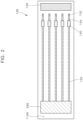
FIG. 2 is a top view of the protection circuit module according to the embodiment of the present invention; -
FIG. 3 is a bottom view of the protection circuit module according to the embodiment of the present invention; -
FIG. 4 is a circuit diagram including an overvoltage protection element according to an embodiment of the present invention; -
FIG. 5 is a circuit diagram of a conventional protection circuit module; -
FIG. 6 is a circuit diagram of a protection circuit module according to an embodiment of the present invention; and -
FIG. 7 is a block diagram of a battery pack according to an embodiment of the present invention. - Hereinafter, exemplary embodiments of the present invention will be described, in detail, with reference to the accompanying drawings. The terms or words used in this specification and claims should not be construed as being limited to the usual or dictionary meaning and should be interpreted as having meanings and concepts consistent with the technical idea of the present invention based on the principle that the inventor can be his/her own lexicographer to appropriately define the concept of the term to explain his/her invention in the best way. The embodiments described in this specification and the configurations shown in the drawings are only some of the embodiments of the present invention and may not represent all of the technical ideas, aspects, and features of the present invention. Accordingly, it should be understood that there may be various equivalents and modifications that can replace or modify the embodiments described herein at the time of filing this application. It will be further understood that the terms "includes," "including," "comprises," and/or "comprising," when used in this specification, specify the presence of stated features, integers, steps, operations, elements, and/or components but do not preclude the presence or addition of one or more other features, integers, steps, operations, elements, components, and/or groups thereof. Further, the use of "may" when describing embodiments of the present invention relates to "one or more embodiments of the present invention."
- In the figures, dimensions of the various elements, layers, etc. may be exaggerated for clarity of illustration. The same reference numerals designate the same elements.
- References to two compared elements, features, etc. as being "the same," may mean that they are "substantially the same." Thus, the phrase "substantially the same" may include a case having a deviation that is considered low in the art, for example, a deviation of 5% or less. In addition, when a certain parameter is referred to as being uniform in a given region, it may mean that it is uniform in terms of an average.
- It will be understood that, although the terms first, second, third, etc. may be used herein to describe various elements, components, regions, layers, and/or sections, these elements, components, regions, layers, and/or sections should not be limited by these terms. These terms are used to distinguish one element, component, region, layer, or section from another element, component, region, layer, or section. Thus, a first element, component, region, layer, or section discussed below could be termed a second element, component, region, layer, or section without departing from the teachings of example embodiments.
- Throughout the specification, unless otherwise stated, each element may be singular or plural.
- When an arbitrary element is referred to as being disposed (or located or positioned) "above" (or "below") or "on" (or "under") a component, it may mean that the arbitrary element is placed in contact with the upper (or lower) surface of the component and may also mean that another component may be interposed between the component and any arbitrary element disposed (or located or positioned) on (or under) the component.
- In addition, it will be understood that, when an element is referred to as being "coupled," "linked" or "connected" to another element, the elements may be directly "coupled," "linked" or "connected" to each other, or an intervening element may be present therebetween, through which the element may be "coupled," "linked" or "connected" to another element. In addition, when a part is referred to as being "electrically coupled" to another part, the part can be directly connected to another part or an intervening part may be present therebetween such that the part and another part are indirectly connected to each other.
- Throughout the specification, when "A and/or B" is stated, it means A, B or A and B, unless otherwise stated. That is, "and/or" includes any or all combinations of a plurality of items enumerated. When "C to D" is stated, it means C or more and D or less, unless otherwise specified.
- Referring to
FIG. 1 to FIG. 3 , aprotection circuit module 100 according to an embodiment of the present invention may include asubstrate 110, aconnector 120, at least oneovervoltage protection element 130, and at least onefuse 140. Theprotection circuit module 100 may include as manyovervoltage protection elements 130 and fuses 140 as battery cells connected to theconnector 120. For example, assuming that the number of battery cells connected to theconnector 120 is five, theprotection circuit module 100 may include fiveovervoltage protection elements 130 and five fuses 140. - The
substrate 110 may have at least one electronic component mounted thereon. According to an embodiment, thesubstrate 110 may be a hard printed circuit board or a flexible printed circuit board. According to an embodiment, thesubstrate 110 may be a double-sided printed circuit board or a multilayer printed circuit board. - The
substrate 110 may include a plurality of layers. The plurality of layers may include a first outer layer formed on afirst surface 110A of thesubstrate 110, and a second outer layer formed on asecond surface 110B of thesubstrate 110 opposite thefirst surface 110A of thesubstrate 110. Thefirst surface 110A may be an upper surface of thesubstrate 110. Thesecond surface 110B may be a lower side of thesubstrate 110. The plurality of layers may include at least one inner layer disposed between the first outer layer and the second outer layer. - The
substrate 110 may include at least one insulating layer. The insulating layer may be disposed between layers having conductive regions formed therein to prevent or substantially reduce interlayer current from flowing in regions other than the conductive vias. The insulating layer may be formed of an insulating material. - The
substrate 110 may include a conductive region 150. The conductive region 150 may be disposed in at least one of the plurality of layers included in thesubstrate 110. The conductive region 150 may be disposed in at least one of the first outer layer, the second outer layer, and the inner layer. The conductive regions 150 may electrically connect the electronic components mounted on thesubstrate 110 to each other. The conductive region 150 may electrically connect at least one electronic component mounted on thesubstrate 110 to external electronic components. - According to an embodiment, the conductive region 150 may be formed of copper, aluminum, silver, tin, gold, nickel, lead, titanium, or an alloy thereof. However, it should be understood that the material for the conductive region 150 is not limited thereto and the conductive region 150 may be formed of a variety of conductive materials.
- According to an embodiment, the conductive region 150 may include at least one first conductive via 151, at least one second conductive via 152, at least one first
conductive line 153, at least one secondconductive line 154, and at least one thirdconductive line 155. Thesubstrate 110 may include as many firstconductive vias 151, secondconductive vias 152, firstconductive lines 153, secondconductive lines 154, and thirdconductive lines 155 as the battery cells connected to theconnector 120. For example, assuming that the number of battery cells connected to theconnector 120 is five, thesubstrate 110 may include five of each of the first conductive via 151, the second conductive via 152, the firstconductive line 153, the secondconductive line 154, and the thirdconductive line 155. - The first conductive via 151 may be formed to extend through the
first surface 110A and thesecond surface 110B of thesubstrate 110. The first conductive via 151 may be formed in a region under or around the region where theconnector 120 is disposed. The first conductive via 151 may be connected to theconnector 120. - The second conductive via 152 may be formed to extend through the
first surface 110A and thesecond surface 110B of thesubstrate 110. The second conductive via 152 may be formed at a location spaced apart from the first conductive via 151 by a predetermined distance in a longitudinal direction of thesubstrate 110. - The first
conductive line 153 may be disposed on thesecond surface 110B of thesubstrate 110. The firstconductive line 153 may be disposed on the second outer layer of thesubstrate 110. The firstconductive line 153 may also be disposed on the inner layer of thesubstrate 110. The firstconductive line 153 may be connected at one end thereof to the first conductive via 151 and at the other end thereof to the second conductive via 152. The firstconductive line 153 may be connected to theovervoltage protection element 130. - The second
conductive line 154 may be disposed on thefirst surface 110A of thesubstrate 110. The secondconductive line 154 may be disposed on the first outer layer of thesubstrate 110. The secondconductive line 154 may also be disposed on the inner layer of thesubstrate 110. The secondconductive line 154 may be connected at one end thereof to the second conductive via 152 and at the other end thereof to thefuse 140. - The third
conductive line 155 may be disposed on thefirst surface 110A of thesubstrate 110. The thirdconductive line 155 may be disposed on the first outer layer of thesubstrate 110. The thirdconductive line 155 may also be disposed on the inner layer of thesubstrate 110. The thirdconductive line 155 may be connected at one end thereof to thefuse 140 and at the other end thereof to an analog front end integrated circuit (AFE IC) 200. TheAFE IC 200 may detect at least one of temperature, voltage, and current of each of the battery cells connected to theconnector 120, and may output a detection result to an external device (for example, a controller of a battery management device). - The
substrate 110 may include a ground region (ground) 160. Theground region 160 may be disposed on thesecond surface 110B of thesubstrate 110. Theground region 160 may be disposed on the second outer layer of thesubstrate 110. Theground region 160 may also be disposed on the inner layer of thesubstrate 110. According to an embodiment, theground region 160 may be formed at a location spaced apart from the first conductive line by a predetermined distance in the longitudinal direction of thesubstrate 110. - The
connector 120 may be disposed on thefirst surface 110A of thesubstrate 110. Theconnector 120 may be disposed on the first outer layer. Theconnector 120 may be a device for connecting at least one battery cell to theAFE IC 200. Theconnector 120 may electrically connect at least one battery cell to theAFE IC 200. Theconnector 120 may include at least one terminal configured to be connected to the battery cell. The terminal may be connected to the battery cell via a wire or a bus. Theconnector 120 may include a terminal configured to be connected to a B+ high current line and a terminal configured to be connected to a B- high current line. Theconnector 120 may be connected to the first conductive via 151. - The
overvoltage protection element 130 may be disposed on thesecond surface 110B. Theovervoltage protection element 130 may be disposed on the second outer layer. According to an embodiment, theovervoltage protection element 130 may include a transient voltage suppressor (TVS) diode. However, it should be understood that theovervoltage protection element 130 is not limited thereto and various devices capable of limiting voltage applied to theconnector 120 may be employed as theovervoltage protection element 130. - The
overvoltage protection element 130 may be conducted when a voltage of a preset magnitude or more is applied. Depending on conduction of theovervoltage protection element 130, part of the voltage applied to theconnector 120 may be absorbed by theovervoltage protection element 130, thereby preventing or substantially reducing excessive voltage from being applied to theAFE IC 200. Theovervoltage protection element 130 may be connected at one end thereof to the firstconductive line 153 and at the other end thereof to theground region 160. - The
fuse 140 may be disposed on thefirst surface 110A. Thefuse 140 may be disposed on the first outer layer. When a current exceeding a preset threshold is applied thereto (i.e., upon occurrence of overcurrent), thefuse 140 may be melted and disconnected to protect theAFE IC 200 from the overcurrent. Thefuse 140 may be connected at one end thereof to the secondconductive line 154 and connected at the other end thereof to the thirdconductive line 155. -
FIG. 4 is a circuit diagram including an overvoltage protection element according to an embodiment of the present invention. - Referring to
FIG. 4 , in a circuit in which anovervoltage protection element 420 is connected between aconnector 410 and anAFE IC 430, if a voltage due to electrostatic discharge (ESD) is applied to theconnector 410, the voltage (voltage at node A) applied to theAFE IC 430 may be defined by Equation 1:
- Here, VESD is the voltage (voltage at node A) applied to the
AFE IC 430 due to electrostatic discharge, VBR_TVS is the breakdown voltage of the overvoltage protection element 420 (voltage at which theovervoltage protection element 420 starts to clamp), RDYN_TVS is the internal resistance of theovervoltage protection element 420, IESD is the current flowing in theovervoltage protection element 420, and L may mean inductance of the overall circuit. - It can be seen from Equation 1 that, when inductance components L1 , L3 of the protection circuit module 400 increase, the voltage VESD applied to the
AFE IC 430 during electrostatic discharge increases. Thus, in order to reduce the voltage applied to theAFE IC 430 upon electrostatic discharge, it is necessary to reduce the inductance components L1 and L3 of the protection circuit module 400. -
FIG. 5 is a circuit diagram of a conventional protection circuit module. Referring toFIG. 5 , a protection circuit module 500, in which aconnector 510, afuse 520, and anovervoltage protection element 530 are all disposed on the upper surface of the substrate, has a circuit configuration in the order of theconnector 510, thefuse 520, theovervoltage protection element 530, and theAFE IC 540. With the circuit configuration shown inFIG. 5 , the protection circuit module 500 has a significant distance between theconnector 510 and theovervoltage protection element 530, causing increase in inductance component L1 of the circuit. In addition, the protection circuit module 500 having the circuit configuration shown inFIG. 5 requires a separate conductive via to connect theovervoltage protection element 530 disposed on the upper surface of the substrate to the ground region disposed on the lower surface of the substrate, thereby increasing the inductance component L3 of the circuit.Table 1 Application of first channel ESD Application of second channel ESD Application of third channel ESD First channel voltage 2216 V 1953 V 2034 V Second channel voltage 2007 V 2091 V 2039 V Third channel voltage 2004 V 1960 V 2247 V - Table 1 shows voltages measured at the
AFE IC 540 when an electrostatic discharge voltage of 27 kV is applied to the protection circuit module 500. From Table 1, it can be seen that, when an electrostatic discharge voltage of 27 kV is applied to three terminals included in theconnector 510, a maximum of 2247 V is applied to theAFE IC 540 in the protection circuit module 500. -
FIG. 6 is a circuit diagram of a protection circuit module according to an embodiment of the present invention. A protection circuit module 600, in which aconnector 610 and afuse 630 are disposed on the upper surface of the substrate and anovervoltage protection element 620 is disposed on the lower surface of the substrate, has a circuit configuration in the order of theconnector 610, theovervoltage protection element 620, thefuse 630, and theAFE IC 640, as shown inFIG. 6 . The protection circuit module 600 can reduce the distance between theconnector 610 and theovervoltage protection element 620, thereby reducing the inductance component L1 of the circuit, as compared to a typical conventional circuit. Further, since both theovervoltage protection element 620 and the ground region are disposed on the lower surface of the substrate, the protection circuit module 600 does not require a separate conductive via to connect theovervoltage protection element 620 to the ground region, whereby the inductance component L3 of the circuit can be reduced. As such, by reducing the inductance component of the protection circuit module 600, the protection circuit module 600 can reduce the voltage applied to theAFE IC 640 in the event of electrostatic discharge.Table 2 Application of first channel ESD Application of second channel ESD Application of third channel ESD First channel voltage 1841 V 1727 V 1720 V Second channel voltage 1772 V 1887 V 1768 V Third channel voltage 1718 V 1732 V 1895 V - Table 2 shows voltages measured at the
AFE IC 640 when an electrostatic discharge voltage of 27 kV is applied to the protection circuit module 600 according to this embodiment. From Table 2, it can be seen that, when an electrostatic discharge voltage of 27 kV is applied to the three terminals included in theconnector 610, a maximum of 1895 V is applied toAFE IC 640 in the protection circuit module 600. -
FIG. 7 is a block diagram of a battery pack. Referring toFIG. 7 , abattery pack 700 according to an embodiment of the present invention has a structure that can be electrically connected to an external device through a cathode connection terminal P(+) and an anode connection terminal P(-). When the external device is a load, thebattery pack 700 is discharged by acting as a power source to provide power to the load. The external device operating as a load may be, for example, an electronic device, a mobile vehicle, or an energy storage system (ESS). Here, the mobile vehicle may be, for example, an electric vehicle, a hybrid vehicle, or a smart mobility device. - The
battery pack 700 may include a plurality ofbattery cells 710, aprotection circuit module 720, and anAFE IC 730. Obviously, in various embodiments, thebattery pack 700 may further include other components. - The plurality of
battery cells 710 may be connected to each other in series or in parallel to constitute at least one battery module. The battery module may include a plurality ofbattery cells 710 and a module housing. The battery modules may be connected to each other in series or in parallel. - The
battery cells 710 may be stacked and received in the module housing. Thebattery cells 710 may include cathode leads and anode leads. Thebattery cells 710 may be round, prismatic, or pouch type battery cells depending on the shape of the battery. - The
battery pack 700 may include a single stack of cells stacked to form a single module instead of the battery modules. The cell stack may be received in an accommodation space of the pack housing, or in an accommodation space partitioned by a frame, a partition wall, or the like. - The
battery cell 710 may generate a large amount of heat during charging/discharging. The generated heat may be accumulated in thebattery cell 710 to promote degradation of thebattery cell 710. Accordingly, thebattery pack 700 may further include a cooling member to inhibit degradation of thebattery cell 710. The cooling member may be disposed at a lower portion of the accommodation space which receives thebattery cells 710. Alternatively, the cooling member may be disposed at an upper portion or a side surface thereof depending on the battery pack. - Exhaust gas generated inside the
battery cell 710 due to an abnormal operating condition, also known as thermal runaway or thermal events in thebattery cell 710, may be discharged from thebattery cell 710. Thebattery pack 700 or the battery module may include an exhaust vent or the like for discharging the exhaust gas to suppress damage to thebattery pack 700 or module due to the exhaust gas. - The
protection circuit module 720 may be a device for protecting theAFE IC 730 from hazards, such as overvoltage, overcurrent, and the like. Theprotection circuit module 720 may be electrically connected to the plurality ofbattery cells 710. Theprotection circuit module 720 may be electrically connected to theAFE IC 730. Theprotection circuit module 720 may be disposed in a path connecting the plurality ofbattery cells 710 and theAFE IC 730. - The
AFE IC 730 may detect at least one of temperature, voltage, and current for each of thebattery cells 710 connected to the connector, and may output a detection result to an external source (for example, a battery management device). TheAFE IC 730 may correspond to components constituting a battery management device. TheAFE IC 730 may transmit information about the results of detecting at least one of temperature, voltage, and current of each of thebattery cells 710 to other components of the battery management device (for example, a balancing device, a control device). TheAFE IC 730 may be electrically connected to theprotection circuit module 720. - The
battery pack 700 may include a battery and a battery management system (BMS) for managing the battery. The battery management device may include a detection device, a balancing device, and a control device. - The detection device may sense a state (for example, voltage, current, temperature, etc.) of the battery and detect state information indicative of the state of the battery. The
AFE IC 730 may correspond to the detection device. The detection device may detect a voltage of each cell or each battery module constituting the battery. The detection device may also detect a current flowing in the battery module or in each of the battery modules constituting thebattery pack 700. The detection device may detect a cell, module and/or ambient temperature at at least one point of the battery. - The balancing device may perform a balancing operation of the battery modules and/or cells constituting the battery. The control device may receive the state information (for example, voltage, current, temperature, etc.) of the battery modules from the detection device. The control device may monitor and calculate a state (for example, voltage, current, temperature, state of charge (SOC), state of health (SOH), etc.) of the battery module based on the state information received from the detection device. Based on the state monitoring results, the control device may perform a control function (for example, temperature control, balancing control, charge/discharge control, etc.), a protection function (for example, over-discharge protection, over-charge protection, over-current protection, short circuit protection, fire extinguishing, and the like), and the like.
- The control unit may perform a wired or wireless communication function with external devices of the battery pack 700 (for example, a higher-level controller or vehicle, a charger, PCS, or the like.). The control device may also control a charge/discharge operation and/or a protection operation of the battery.
- The battery management device is a system that monitors battery states, performs diagnostics and control, communication and protection functions, and may calculate a charge/discharge state, calculate battery life or state of health (SOH), cut off battery power as needed (relay control), control thermal management (cooling, heating, etc.), perform high-voltage interlock functions, and detect insulation and short circuit conditions.
- Here, the relay control may be a function to cut off power supply from the battery in the event of a problem with a vehicle and a battery system. Each of the cathode and the anode may be provided with one or more relays and pre-charge relays. The high-voltage interlock function may be a function that forces the relay to open when there is an opening in the entire loop.
- As described above, according to the present invention, the protection circuit module has a circuit configuration in the order of the connector, the fuse, and the overvoltage protection element to reduce inductance components of the protection circuit module, thereby improving overvoltage protection performance of the protection circuit module.
- Herein, the embodiments described herein may be implemented, for example, as a method or process, a device, a software program, a data stream, or a signal. Although discussed in the context of a single type of implementation (for example, discussed only as a method), features discussed herein may also be implemented in other forms (for example, a device or a program). The device may be implemented by suitable hardware, software, firmware, and the like. The method may be implemented on a device, such as a processor that generally refers to a processing device including a computer, a microprocessor, an integrated circuit, a programmable logic device, etc. The processor includes a communication device such as a computer, a cell phone, a personal digital assistant (PDA), and other devices that facilitate communication of information between the device and end-users.
- Although the present invention has been described with reference to some embodiments and drawings illustrating aspects thereof, the present invention is not limited thereto. Various modifications and variations can be made by a person skilled in the art to which the present invention belongs within the scope of the technical features of the invention as set forth by the appended claims.
Claims (15)
- A protection circuit module (100, 400, 500, 600, 720) comprising:a substrate (110) having a first surface (110A) and a second surface (110B);a connector (120, 410, 510, 610) disposed on the first surface (110A) and electrically connected to a battery cell (710);an overvoltage protection element (130, 420, 530, 620) disposed on the second surface (110B) and electrically connected to the connector (120, 410, 510, 610); anda fuse (140, 520, 630) disposed on the first surface (110A) and electrically connected to the overvoltage protection element (130, 420, 530, 620).
- The protection circuit module (100, 400, 500, 600, 720) according to claim 1, wherein the substrate (110) comprises a first and second conductive via (151, 152) extending through the first surface (110A) and the second surface (110B); a first conductive line (153) disposed on the second surface (110B) and electrically connected to the first and second conductive via (151, 152); and a second conductive line (154) disposed on the first surface (110A) and electrically connected to the second conductive via (152).
- The protection circuit module (100, 400, 500, 600, 720) according to claim 2, wherein the connector (120, 410, 510, 610) is electrically connected to the first conductive via (151).
- The protection circuit module (100, 400, 500, 600, 720) according to claim 2 or 3, wherein the overvoltage protection element (130, 420, 530, 620) is electrically connected to the first conductive line (153).
- The protection circuit module (100, 400, 500, 600, 720) according to any one of claims 2 to 4, wherein the substrate (110) further comprises a ground region (160) disposed on the second surface (110B) and the overvoltage protection element (130, 420, 530, 620) is electrically connected to the ground region (160).
- The protection circuit module (100, 400, 500, 600, 720) according to any one of claims 2 to 5, wherein the fuse (140, 520, 630) is electrically connected to the second conductive line (154).
- The protection circuit module (100, 400, 500, 600, 720) according to any one of the preceding claims, further comprising:
an analog front end integrated circuit, AFE IC, (200, 430, 540, 640, 730) disposed on the first surface (110A) and electrically connected to the fuse (140, 520, 630). - The protection circuit module (100, 400, 500, 600, 720) according to any one of the preceding claims, wherein the overvoltage protection element (130, 420, 530, 620) comprises a transient voltage suppressor, TVS.
- A battery pack (700) comprising:a battery cell (710);an analog front end integrated circuit, AFE IC (200, 430, 540, 640, 730); anda protection circuit module (100, 400, 500, 600, 720) electrically connecting the battery cell (710) to the AFE IC (200, 430, 540, 640, 730) and protecting the AFE IC (200, 430, 540, 640, 730) from electrostatic discharge,wherein the protection circuit module (100, 400, 500, 600, 720) comprises:a substrate (110) having a first surface (110A) and a second surface (110B);a connector (120, 410, 510, 610) disposed on the first surface (110A) and electrically connected to a battery cell (710);an overvoltage protection element (130, 420, 530, 620) disposed on the second surface (110B) and electrically connected to the connector (120, 410, 510, 610); anda fuse (140, 520, 630) disposed on the first surface (110A) and electrically connected to the overvoltage protection element (130, 420, 530, 620).
- The battery pack (700) according to claim 9, wherein the substrate (110) comprises a first and second conductive via (151, 152) extending through the first surface (110A) and the second surface (110B); a first conductive line (153) disposed on the second surface (110B) and electrically connected to the first and second conductive via (151, 152); and a second conductive line (154) disposed on the first surface (110A) and electrically connected to the second conductive via (152).
- The battery pack (700) according to claim 10, wherein the connector (120, 410, 510, 610) is electrically connected to the first conductive via (151).
- The battery pack (700) according to claim 10 or 11, wherein the overvoltage protection element (130, 420, 530, 620) is electrically connected to the first conductive line (153).
- The battery pack (700) according to any one of claims 10 to 12, wherein the substrate (110) further comprises a ground region (160) disposed on the second surface (110B) and the overvoltage protection element (130, 420, 530, 620) is electrically connected to the ground region (160).
- The battery pack (700) according to any one of claims 10 to 13, wherein the fuse (140, 520, 630) is electrically connected to the second conductive line (154).
- The battery pack (700) according to any one of claims 9 to 14, wherein the overvoltage protection element (130, 420, 530, 620) comprises a transient voltage suppressor, TVS.
Applications Claiming Priority (1)
| Application Number | Priority Date | Filing Date | Title |
|---|---|---|---|
| KR1020230143778A KR20250059806A (en) | 2023-10-25 | 2023-10-25 | Protection circuit module and battery pack comprising the same |
Publications (1)
| Publication Number | Publication Date |
|---|---|
| EP4546501A1 true EP4546501A1 (en) | 2025-04-30 |
Family
ID=90123749
Family Applications (1)
| Application Number | Title | Priority Date | Filing Date |
|---|---|---|---|
| EP24160413.1A Pending EP4546501A1 (en) | 2023-10-25 | 2024-02-29 | Protection circuit module and battery pack including the same |
Country Status (5)
| Country | Link |
|---|---|
| US (1) | US12603492B2 (en) |
| EP (1) | EP4546501A1 (en) |
| JP (1) | JP2025073042A (en) |
| KR (1) | KR20250059806A (en) |
| CN (1) | CN119891423A (en) |
Citations (3)
| Publication number | Priority date | Publication date | Assignee | Title |
|---|---|---|---|---|
| EP2955848A1 (en) * | 2014-04-23 | 2015-12-16 | NGK Spark Plug Co., Ltd. | Control apparatus |
| US20220094109A1 (en) * | 2019-09-11 | 2022-03-24 | Lg Energy Solution, Ltd. | Connector Integrated With Protection Element |
| WO2022163478A1 (en) * | 2021-01-29 | 2022-08-04 | 三洋電機株式会社 | Power source device and method for manufacturing same |
Family Cites Families (4)
| Publication number | Priority date | Publication date | Assignee | Title |
|---|---|---|---|---|
| US7083425B2 (en) * | 2004-08-27 | 2006-08-01 | Micron Technology, Inc. | Slanted vias for electrical circuits on circuit boards and other substrates |
| US10021784B1 (en) * | 2017-12-19 | 2018-07-10 | Powertech Technology Inc. | Electronic device and electronic circuit board thereof |
| TWI845799B (en) * | 2020-12-28 | 2024-06-21 | 方略電子股份有限公司 | Substrate structure and electronic device |
| AU2022212078A1 (en) | 2021-01-29 | 2023-09-14 | Aak Ab | Cheese-analogue composition |
-
2023
- 2023-10-25 KR KR1020230143778A patent/KR20250059806A/en active Pending
-
2024
- 2024-01-19 US US18/417,218 patent/US12603492B2/en active Active
- 2024-02-08 JP JP2024017814A patent/JP2025073042A/en active Pending
- 2024-02-29 EP EP24160413.1A patent/EP4546501A1/en active Pending
- 2024-04-10 CN CN202410426623.9A patent/CN119891423A/en active Pending
Patent Citations (4)
| Publication number | Priority date | Publication date | Assignee | Title |
|---|---|---|---|---|
| EP2955848A1 (en) * | 2014-04-23 | 2015-12-16 | NGK Spark Plug Co., Ltd. | Control apparatus |
| US20220094109A1 (en) * | 2019-09-11 | 2022-03-24 | Lg Energy Solution, Ltd. | Connector Integrated With Protection Element |
| WO2022163478A1 (en) * | 2021-01-29 | 2022-08-04 | 三洋電機株式会社 | Power source device and method for manufacturing same |
| EP4287352A1 (en) * | 2021-01-29 | 2023-12-06 | Panasonic Energy Co., Ltd. | Power source device and method for manufacturing same |
Also Published As
| Publication number | Publication date |
|---|---|
| US12603492B2 (en) | 2026-04-14 |
| JP2025073042A (en) | 2025-05-12 |
| US20250141212A1 (en) | 2025-05-01 |
| KR20250059806A (en) | 2025-05-07 |
| CN119891423A (en) | 2025-04-25 |
Similar Documents
| Publication | Publication Date | Title |
|---|---|---|
| US10381633B2 (en) | Busbar | |
| US6713210B1 (en) | Secondary cell protection circuit device and secondary cell assembly | |
| US20060076923A1 (en) | Methods and systems for assembling batteries | |
| EP2293361A2 (en) | Middle or large-sized battery pack with improved safety | |
| KR20150121518A (en) | Battery module and battery pack for guarantee at safety for short circuit | |
| KR20150121519A (en) | Battery Module and Battery Pack having welding structure for guarantee at safety for short circuit | |
| CN220138652U (en) | Battery pack and electric equipment | |
| US20140272492A1 (en) | Safety device for a galvanic cell | |
| US12603492B2 (en) | Protection circuit module and battery pack including the same | |
| EP4621932A1 (en) | Charging control method and apparatus for battery | |
| US20220029427A1 (en) | Pre-charge unit for charging a dc link capacitor and battery system including the same | |
| CN103620821A (en) | Connector for producing an electrically conductive connection between at least three terminals of battery cells | |
| KR20040037547A (en) | Secondary battery pack | |
| CN207542296U (en) | A kind of battery modules | |
| EP4664659A1 (en) | Battery system including improved electrical connecting elements | |
| KR20070108758A (en) | Battery pack manufacturing device | |
| US20250118869A1 (en) | Battery module | |
| EP4607668A1 (en) | Battery cells and battery modules | |
| US11108119B2 (en) | Fusible link design for lithium-ion 18650 cells | |
| CN107742685B (en) | Battery module | |
| EP4557446A2 (en) | Rechargeable battery and rechargeable battery module | |
| TWM673691U (en) | Active thermal runaway protection for lithium-ion battery modules | |
| US20250286208A1 (en) | Secondary battery and secondary battery module including the same | |
| EP4648182A1 (en) | Battery module | |
| CN210778876U (en) | Battery package protection plate and battery package |
Legal Events
| Date | Code | Title | Description |
|---|---|---|---|
| PUAI | Public reference made under article 153(3) epc to a published international application that has entered the european phase |
Free format text: ORIGINAL CODE: 0009012 |
|
| STAA | Information on the status of an ep patent application or granted ep patent |
Free format text: STATUS: REQUEST FOR EXAMINATION WAS MADE |
|
| 17P | Request for examination filed |
Effective date: 20240229 |
|
| AK | Designated contracting states |
Kind code of ref document: A1 Designated state(s): AL AT BE BG CH CY CZ DE DK EE ES FI FR GB GR HR HU IE IS IT LI LT LU LV MC ME MK MT NL NO PL PT RO RS SE SI SK SM TR |