EP4546394A1 - Electron microscopy detector - Google Patents
Electron microscopy detector Download PDFInfo
- Publication number
- EP4546394A1 EP4546394A1 EP23206066.5A EP23206066A EP4546394A1 EP 4546394 A1 EP4546394 A1 EP 4546394A1 EP 23206066 A EP23206066 A EP 23206066A EP 4546394 A1 EP4546394 A1 EP 4546394A1
- Authority
- EP
- European Patent Office
- Prior art keywords
- detector modules
- detection unit
- imaging device
- module
- configuration
- Prior art date
- Legal status (The legal status is an assumption and is not a legal conclusion. Google has not performed a legal analysis and makes no representation as to the accuracy of the status listed.)
- Granted
Links
Images





Classifications
-
- H—ELECTRICITY
- H01—ELECTRIC ELEMENTS
- H01J—ELECTRIC DISCHARGE TUBES OR DISCHARGE LAMPS
- H01J37/00—Discharge tubes with provision for introducing objects or material to be exposed to the discharge, e.g. for the purpose of examination or processing thereof
- H01J37/02—Details
- H01J37/244—Detectors; Associated components or circuits therefor
-
- H—ELECTRICITY
- H01—ELECTRIC ELEMENTS
- H01J—ELECTRIC DISCHARGE TUBES OR DISCHARGE LAMPS
- H01J37/00—Discharge tubes with provision for introducing objects or material to be exposed to the discharge, e.g. for the purpose of examination or processing thereof
- H01J37/02—Details
- H01J37/023—Means for mechanically adjusting components not otherwise provided for
-
- H—ELECTRICITY
- H01—ELECTRIC ELEMENTS
- H01J—ELECTRIC DISCHARGE TUBES OR DISCHARGE LAMPS
- H01J37/00—Discharge tubes with provision for introducing objects or material to be exposed to the discharge, e.g. for the purpose of examination or processing thereof
- H01J37/26—Electron or ion microscopes; Electron or ion diffraction tubes
- H01J37/28—Electron or ion microscopes; Electron or ion diffraction tubes with scanning beams
-
- H—ELECTRICITY
- H01—ELECTRIC ELEMENTS
- H01J—ELECTRIC DISCHARGE TUBES OR DISCHARGE LAMPS
- H01J2237/00—Discharge tubes exposing object to beam, e.g. for analysis treatment, etching, imaging
- H01J2237/05—Arrangements for energy or mass analysis
-
- H—ELECTRICITY
- H01—ELECTRIC ELEMENTS
- H01J—ELECTRIC DISCHARGE TUBES OR DISCHARGE LAMPS
- H01J2237/00—Discharge tubes exposing object to beam, e.g. for analysis treatment, etching, imaging
- H01J2237/244—Detection characterized by the detecting means
- H01J2237/24455—Transmitted particle detectors
-
- H—ELECTRICITY
- H01—ELECTRIC ELEMENTS
- H01J—ELECTRIC DISCHARGE TUBES OR DISCHARGE LAMPS
- H01J2237/00—Discharge tubes exposing object to beam, e.g. for analysis treatment, etching, imaging
- H01J2237/244—Detection characterized by the detecting means
- H01J2237/2446—Position sensitive detectors
-
- H—ELECTRICITY
- H01—ELECTRIC ELEMENTS
- H01J—ELECTRIC DISCHARGE TUBES OR DISCHARGE LAMPS
- H01J2237/00—Discharge tubes exposing object to beam, e.g. for analysis treatment, etching, imaging
- H01J2237/244—Detection characterized by the detecting means
- H01J2237/2446—Position sensitive detectors
- H01J2237/24465—Sectored detectors, e.g. quadrants
-
- H—ELECTRICITY
- H01—ELECTRIC ELEMENTS
- H01J—ELECTRIC DISCHARGE TUBES OR DISCHARGE LAMPS
- H01J2237/00—Discharge tubes exposing object to beam, e.g. for analysis treatment, etching, imaging
- H01J2237/26—Electron or ion microscopes
- H01J2237/28—Scanning microscopes
- H01J2237/2802—Transmission microscopes
Definitions
- the invention relates but is not limited to imaging devices for a scanning transmission electron microscope.
- the invention also relates to corresponding method for operating such an imaging devices.
- a conventional STEM may comprise a pixelated detection unit (for example, a unit of 128x128 pixels, 192x192 pixels, or of 264x264 pixels).
- the detection unit is conventionally configured to receive the electrons after they have been transmitted through the sample under inspection.
- Such conventional STEMs comprising such a pixelated detection unit have two main drawbacks.
- the first drawback is the very high data-rate needed to support a readout of the pixelated detection unit (up to 200 TB.hr -1 ).
- the second drawback is that the majority of pixelated detection units do not allow, in practice, an electron energy-loss spectroscopy (EELS) of good quality, as most do not incoporate a central hole.
- Some pixelated detection units comprise a hole at their centre to allow a central portion of the electron beam to pass and be used for electron energy-loss spectroscopy (EELS).
- EELS electron energy-loss spectroscopy
- Figure 1A and Figure 1B schematically show an imaging device 1 for a scanning transmission electron microscope 2.
- the imaging device 1 comprises a detection unit 3.
- the detection unit 3 is configured to receive electrons 10 after they have been transmitted through a sample 4 under inspection.
- the detection unit 3 comprises a plurality of pixelated detector modules 5.
- the detection unit 3 further comprises means 6 for mutually displacing the plurality of detector modules 5 between at least two configurations.
- a first configuration of the plurality of detector modules 5 is represented in Figure 1A .
- the plurality of detector modules 5 are adjacent to each other such that there is no hole in the detection unit 3.
- a second configuration of the plurality of detector modules 5 is represented in Figure 1B .
- the plurality of detector modules 5 are mutually displaced with respect to each other such that there is a hole 7 in the detection unit 3.
- the imaging device of the disclosure is thus a hybrid device and comprises a full configuration and/or a holed configuration.
- Figures 2A and 2B schematically show that the means 6 for mutually displacing the plurality of detector modules 5 are configured to mutually displace the detector modules 5 from a first configuration ( Figure 2A ) to a second configuration ( Figure 2B ) or vice versa.
- a hole 7 has a first desired area S 1 .
- the detection unit 3 occupies a larger total area than in the first configuration, due to the displacement of detector modules 5 (indicated schematically by arrows) to provide a hole 7. Examples of how the detection modules 5 may be displaced are described below with reference to Figures 3A-4C .
- Figures 2B and 2C schematically show that the means 6 for mutually displacing the plurality of detector modules 5 are configured to mutually displace the detector modules 5 from the second configuration ( Figure 2B ) to a third configuration ( Figure 2C ) or vice versa, or between the third configuration ( Figure 2C ) and the first configuration ( Figure 2A ).
- Figures 2B and 2C schematically show that the means 6 for mutually displacing the plurality of detector modules 5 are configured to mutually displace the detector modules 5 from the second configuration ( Figure 2B ) to a third configuration ( Figure 2C ) or vice versa, or between the third configuration ( Figure 2C ) and the first configuration ( Figure 2A ).
- the hole 7 has a second desired area S 2 , the second desired area S 2 being different from the first desired area S 1 .
- the detection unit 3 occupies a larger total area than in the first configuration, due to the displacement of detector modules 5 (indicated schematically by arrows) to provide a hole 7.
- the detection unit 3 also occupies a larger total area than in the second configuration.
- Figures 2B and 2C schematically show that the first desired area S 1 (area equivalent to 1 area S p of a pixel 8) and the second desired area S 2 (area equivalent to 4 areas S p of a pixel 8) are such that: 1 4 .
- S p wherein S p is the area of a pixel of the pixelated detector modules.
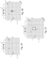
- FIGS 3A and 3B schematically show a detection unit 3 comprising two pixelated detector modules 5.
- each one of the two pixelated detector modules 5 comprises a gridded array of detectors configured to form pixels 8 of the module 5.
- each gridded array is indented on one edge 9 such that the one edge 9 of the gridded array is configured to linearly slidably cooperate with another corresponding edge 9 of the other pixelated detector module 5 of the two pixelated detector modules, in order to open ( Figure 3B ) and close ( Figure 3A ) a hole 7 in the detection unit 3.
- each pixelated detector module 5 has a height of four lines of pixels 8, with three lines having eight pixels 8 and with the edge 9 having four pixels 8 to form the indent.
- the closed detection unit 3 is an array of 7x8 pixels.
- the detection unit 3 has the 1x1 hole 7 and a retained square (shown by the dotted line) of 7x7 pixels.
- the embodiment of Figures 3A and 3B enables accurate Centre of Mass (COM) imaging and EELS ( Figure 3B ).
- FIGs 4A, 4B and 4C schematically show a detection unit 3 comprising four pixelated detector modules 5.
- each one of the four pixelated detector modules 5 comprises a gridded array of detectors configured to form pixels 8 of the module 5.
- the four detector modules 5 are configured to cooperate with each other such that in a first configuration ( Figure 4A ), the four detector modules are adjacent to each other and abut at one point 11, and in a second configuration ( Figures 4B and 4C ), the four detector modules 5 are mutually displaced with respect to each other such that a hole 7 is located at a centre of the detection unit 3, as shown by the dotted lines in Figure 4B and Figure 4C .
- the hole 7 has a first area and the detection unit 3 has a 7x7 pixels square area.
- the hole 7 has a second area, greater than the first area of Figure 4B , and the detection unit 3 has a 6x6 pixel square area.
- the point 11 is also forming the centre of the detection unit 3, the detection unit 3 having a 8x8 square area.
- each pixelated detector module 5 is mounted at a corner of a conforming printed circuit board (not shown in Figures 4A, 4B and 4C ), for two-side tileable cooperation with other detector modules 5 of the detection unit 3.
- the detection unit 3 has thus a 4-fold symmetry at all times, and the embodiment of Figures 4A, 4B and 4C enables accurate COM imaging, EELS ( Figures 4B and 4C ) and differential phase contrast (DPC) imaging.
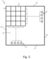
- a pixelated detector module 5 further comprises means 12 for a readout of pixels 8 of the module 5.
- the means 12 for the readout may comprise amplifiers.
- the pixelated detector module 5 is mounted along a portion of each of two edges 13 and 14 of a conforming printed circuit board 15.
- the means 12 for the readout are located along two other edges 16 and 17 of the detector module 5, on the printed circuit board 15.
- the means could be placed at another location, for example on another face of the printed circuit board compared to the detector module.
- the means for the readout are configured to read the detectors individually. In such an example, for a 4x4 module, the number of readouts is 16.
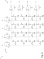
- the means 12 for the readout are configured to read the detectors as whole columns and rows.
- detector signals for the pixels 8 of a 4x4 module are represented by nodes P1 to P16, and for each row and column of pixels, the nodes corresponding to the given row or column or pixels are electrically coupled in parallel to provide a single readout signal for the whole row/column (e.g. via an amplifier electrically coupled in parallel to the row/column nodes).
- the nodes P1, P5, P9 and P13 corresponding to a row of pixels are connected in parallel so as to produce a readout signal x 1 for that row, and the nodes P1 to P4 corresponding to a column of pixels are also connected in parallel so as to produce a readout signal y 1 for that column.
- an event e.g. an incident electron
- the location of an event (i.e., an incident electron) detected on the module 5 is then retrieved as a logical ⁇ AND' of the readouts of a column and a row.
- the means 12 for the readout are configured to read the detectors as whole columns and rows by feeding signal chains of the column readings and the row readings into respective resistor ladders.
- the readout signals x 1 to x 4 for detecting events in the rows of the detector are connected to a row resistor ladder having output voltages V x0 and V x1 at its extremities.
- the readout signals y 1 to y 4 for detecting events in the columns of the detector are connected to a column resistor ladder having output voltages V y0 and V y1 at its extremities.
- the location of a detected event is retrieved by reading out both extremities of each resistor ladder.
- the resistor ladder enables the readout of each resistor ladder (determined by calculating the difference between the extremity voltages) to take a unique value for each combination of row/column signals.
- the row resistor ladder output (determined as V x1 - V x0 ) has a different value for each combination of row readout signals x 1 to x 4 .
- the same principle applies to the column resistor ladder output (V y1 - V y0 ). Therefore, in Figure 7 , the number of readouts is 4 per module, which may further reduce the size of the module 5 and the overall detection unit, and also further reduces the number of high-speed analog-to-digital converters used in the detection unit.
- each pixel 8 of the pixelated detector modules comprises a scintillator 18 (such as a YAG scintillator, but other types are envisaged) configured to convert incident electrons into light pulses, the scintillator 18 being mounted on an avalanche photodiode 19.
- the scintillator 18 is a man-made single-crystal, and the sensitive area can reach right to the edges 13 and 14 of the module 5 as shown in Figure 5 , leading to zero dead-layer around each pixel 8 or around a hole in the detection unit.
- all electrons across the detection plane would either be detected by one of the detector pixels 8 or be available to the EELS spectrometer. This eliminates any dead-layer and provides for more efficient overall information collection. This arrangement also enables readout speeds compliant with scanning transmission electron microscopy.
- each pixel of the pixelated detector modules 5 may have a side length x such that: 1 mm ⁇ x ⁇ 6 mm .
- the imaging device of the disclosure enables the use of a detection unit comprising fewer than 256 pixels, e.g., with modules which are each smaller than, or equal to, an 8x8 matrix.
- the readout of the detection unit of the disclosure has a relatively low data-rate with satisfactory performances, and e.g., the peak signal to noise ratio (PSNR) of a ptychographic phase reconstruction using the detection unit of the disclosure may be as satisfactory as that of a conventional detection unit of e.g., 1024 pixels.
- PSNR peak signal to noise ratio
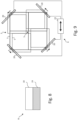
- Figure 9 schematically shows that the means 6 for mutually displacing the plurality of detector modules 5 comprise an actuator 20 configured to move the detector modules 5 cooperatively with respect to each other, such as along a linear or non-linear movement.
- the displacing means 6 comprises a plurality of actuators 20 (e.g. one actuator per detector module) each configured to displace a detector module 5 linearly (e.g. in a direction oriented at 45° to the pixel arrays, as indicated by the arrows).
- the actuator 20 may attach to a location on the module 5 that is distant from the hole 7 formed when displacing the modules 5, such that the displacing means 6 does not interfere with detection of electrons through the hole.
- the actuators 20 may be communicably coupled to a controller 22 configured to control the actuators simultaneously.
- the controller 22 may also be used to receive data from each actuator for feedback control of the detection unit, the data indicative of the position of the detector modules.
- a single actuator 20 may be configured to configured to displace multiple (e.g. all) of the modules 5.
- the detector modules 5 may be connected by a linkage mechanism that can be driven (linearly or otherwise) with a single actuator such that the modules 5 are displaced in their respective directions indicated by the arrows in Figure 9 .
- the movement of all four modules may be synchronised with a single slotted wheel driven by a single actuator.
- the imaging device 1 may further comprise:
- Figure 10 schematically shows a method 100 of operating a detection unit of an imaging device for a scanning transmission electron microscope.
- the method 100 comprises mutually displacing, at S1, a plurality of detector modules of the detection unit to control an area of a hole in the detection unit.
- the detection unit may be a detection unit of any aspects of the disclosure.
- the method 100 further comprises:
Landscapes
- Chemical & Material Sciences (AREA)
- Analytical Chemistry (AREA)
- Analysing Materials By The Use Of Radiation (AREA)
Abstract
Description
- The invention relates but is not limited to imaging devices for a scanning transmission electron microscope. The invention also relates to corresponding method for operating such an imaging devices.
- In a conventional scanning transmission electron microscope (STEM), a focussed beam of electrons is scanned across a sample under inspection. A conventional STEM may comprise a pixelated detection unit (for example, a unit of 128x128 pixels, 192x192 pixels, or of 264x264 pixels). The detection unit is conventionally configured to receive the electrons after they have been transmitted through the sample under inspection.
- Such conventional STEMs comprising such a pixelated detection unit have two main drawbacks.
- The first drawback is the very high data-rate needed to support a readout of the pixelated detection unit (up to 200 TB.hr-1).
- The second drawback is that the majority of pixelated detection units do not allow, in practice, an electron energy-loss spectroscopy (EELS) of good quality, as most do not incoporate a central hole. Some pixelated detection units comprise a hole at their centre to allow a central portion of the electron beam to pass and be used for electron energy-loss spectroscopy (EELS). However, in these cases, a significant amount of electrons are lost in a dead layer surrounding the central hole and are not available for the EELS.
- Aspects and embodiments of the invention are set out in the appended claims. These and other aspects, and embodiments which are helpful in understanding the invention set out in the claims are also described herein.
- Aspects of the disclosure will now be described, by way of example, with reference to the accompanying drawings in which:
-
Figure 1A and Figure 1B schematically show a cross section of an imaging device for a scanning transmission electron microscope; -
Figures 2A, 2B and 2C schematically show a top view of means for mutually displacing the plurality of detector modules between a plurality of configurations; -
Figures 3A and 3B schematically show a top view of a detection unit comprising two pixelated detector modules; -
Figures 4A, 4B and 4C schematically show a top view of a detection unit comprising four pixelated detector modules; -
Figure 5 schematically shows a top view of a detector module comprising means for a readout of the pixels of the module; -
Figures 6 and7 show an electric schematic of means for a readout of the detectors; - In
Figure 8 schematically shows a cross section of a pixel of a pixelated detector module; -
Figure 9 schematically shows means for mutually displacing the plurality of detector modules; -
Figure 10 schematically shows general steps of a method of operating a detection unit. - In the figures, similar elements bear the same numerical reference.
-
Figure 1A and Figure 1B schematically show animaging device 1 for a scanningtransmission electron microscope 2. - In
Figures 1A and 1B , theimaging device 1 comprises adetection unit 3. Thedetection unit 3 is configured to receiveelectrons 10 after they have been transmitted through a sample 4 under inspection. - In
Figures 1A and 1B , thedetection unit 3 comprises a plurality ofpixelated detector modules 5. - In
Figures 1A and 1B , thedetection unit 3 further comprises means 6 for mutually displacing the plurality ofdetector modules 5 between at least two configurations. - A first configuration of the plurality of
detector modules 5 is represented inFigure 1A . InFigure 1A , the plurality ofdetector modules 5 are adjacent to each other such that there is no hole in thedetection unit 3. - A second configuration of the plurality of
detector modules 5 is represented inFigure 1B . InFigure 1B , the plurality ofdetector modules 5 are mutually displaced with respect to each other such that there is ahole 7 in thedetection unit 3. - The imaging device of the disclosure is thus a hybrid device and comprises a full configuration and/or a holed configuration.
-
Figures 2A, 2B and 2C schematically show means 6 for mutually displacing a plurality ofdetector modules 5, which are further configured to mutually displace thedetector modules 5 between at least two configurations and one additional configuration. -
Figures 2A and 2B schematically show that the means 6 for mutually displacing the plurality ofdetector modules 5 are configured to mutually displace thedetector modules 5 from a first configuration (Figure 2A ) to a second configuration (Figure 2B ) or vice versa. - In
Figure 2B , ahole 7 has a first desired area S1. In the second configuration, thedetection unit 3 occupies a larger total area than in the first configuration, due to the displacement of detector modules 5 (indicated schematically by arrows) to provide ahole 7. Examples of how thedetection modules 5 may be displaced are described below with reference toFigures 3A-4C . -
Figures 2B and 2C schematically show that the means 6 for mutually displacing the plurality ofdetector modules 5 are configured to mutually displace thedetector modules 5 from the second configuration (Figure 2B ) to a third configuration (Figure 2C ) or vice versa, or between the third configuration (Figure 2C ) and the first configuration (Figure 2A ). In -
Figure 2C , thehole 7 has a second desired area S2, the second desired area S2 being different from the first desired area S1. In the third configuration, thedetection unit 3 occupies a larger total area than in the first configuration, due to the displacement of detector modules 5 (indicated schematically by arrows) to provide ahole 7. In this example, in the third configuration thedetection unit 3 also occupies a larger total area than in the second configuration. -
Figures 2B and 2C schematically show that the first desired area S1 (area equivalent to 1 area Sp of a pixel 8) and the second desired area S2 (area equivalent to 4 areas Sp of a pixel 8) are such that:
-
Figures 3A and 3B schematically show adetection unit 3 comprising twopixelated detector modules 5. InFigures 3A and 3B , each one of the twopixelated detector modules 5 comprises a gridded array of detectors configured to formpixels 8 of themodule 5. InFigures 3A and 3B , each gridded array is indented on oneedge 9 such that the oneedge 9 of the gridded array is configured to linearly slidably cooperate with anothercorresponding edge 9 of the otherpixelated detector module 5 of the two pixelated detector modules, in order to open (Figure 3B ) and close (Figure 3A ) ahole 7 in thedetection unit 3. InFigures 3A and 3B , eachpixelated detector module 5 has a height of four lines ofpixels 8, with three lines having eightpixels 8 and with theedge 9 having fourpixels 8 to form the indent. InFigure 3A , the closeddetection unit 3 is an array of 7x8 pixels. InFigure 3B , thedetection unit 3 has the 1x1hole 7 and a retained square (shown by the dotted line) of 7x7 pixels. The embodiment ofFigures 3A and 3B enables accurate Centre of Mass (COM) imaging and EELS (Figure 3B ). -
Figures 4A, 4B and 4C schematically show adetection unit 3 comprising fourpixelated detector modules 5. InFigures 4A and 4B , each one of the fourpixelated detector modules 5 comprises a gridded array of detectors configured to formpixels 8 of themodule 5. InFigures 4A, 4B and 4C , the fourdetector modules 5 are configured to cooperate with each other such that in a first configuration (Figure 4A ), the four detector modules are adjacent to each other and abut at onepoint 11, and in a second configuration (Figures 4B and 4C ), the fourdetector modules 5 are mutually displaced with respect to each other such that ahole 7 is located at a centre of thedetection unit 3, as shown by the dotted lines inFigure 4B and Figure 4C . InFigure 4B , thehole 7 has a first area and thedetection unit 3 has a 7x7 pixels square area. InFigure 4C , thehole 7 has a second area, greater than the first area ofFigure 4B , and thedetection unit 3 has a 6x6 pixel square area. InFigure 4A , thepoint 11 is also forming the centre of thedetection unit 3, thedetection unit 3 having a 8x8 square area. - In
Figures 4A, 4B and 4C , eachmodule 5 is a square matrix of detectors, each module having the same number ofpixels 8 as theother modules 5 in thedetector unit 3. InFigures 4A, 4B and 4C , each module is a 4x4 matrix. Other sizes are envisaged, such as an 8x8 matrix. - In
Figures 4A, 4B and 4C , eachpixelated detector module 5 is mounted at a corner of a conforming printed circuit board (not shown inFigures 4A, 4B and 4C ), for two-side tileable cooperation withother detector modules 5 of thedetection unit 3. InFigures 4A, 4B and 4C , thedetection unit 3 has thus a 4-fold symmetry at all times, and the embodiment ofFigures 4A, 4B and 4C enables accurate COM imaging, EELS (Figures 4B and 4C ) and differential phase contrast (DPC) imaging. - In
Figure 5 , apixelated detector module 5 further comprises means 12 for a readout ofpixels 8 of themodule 5. The means 12 for the readout may comprise amplifiers. InFigure 5 , thepixelated detector module 5 is mounted along a portion of each of twoedges circuit board 15. InFigure 5 , themeans 12 for the readout are located along twoother edges detector module 5, on the printedcircuit board 15. However, the means could be placed at another location, for example on another face of the printed circuit board compared to the detector module. - In some examples, the means for the readout are configured to read the detectors individually. In such an example, for a 4x4 module, the number of readouts is 16.
- In
Figure 6 , themeans 12 for the readout are configured to read the detectors as whole columns and rows. In this example circuit, detector signals for thepixels 8 of a 4x4 module are represented by nodes P1 to P16, and for each row and column of pixels, the nodes corresponding to the given row or column or pixels are electrically coupled in parallel to provide a single readout signal for the whole row/column (e.g. via an amplifier electrically coupled in parallel to the row/column nodes). For example, the nodes P1, P5, P9 and P13 corresponding to a row of pixels are connected in parallel so as to produce a readout signal x1 for that row, and the nodes P1 to P4 corresponding to a column of pixels are also connected in parallel so as to produce a readout signal y1 for that column. Accordingly, if a detector detects an event (e.g. an incident electron) and produces an output signal, corresponding x- and y-readouts will be affected. InFigure 6 , the location of an event (i.e., an incident electron) detected on themodule 5 is then retrieved as a logical `AND' of the readouts of a column and a row. For example, if the readouts x1 and y1 both take a non-zero value or change their value, this indicates that the pixel detector corresponding to node P1 has detected an event. InFigure 6 , the number of readouts is 8, which may reduce the size of themodule 5 and the overall detection unit. The detection unit may further comprise high-speed analog-to-digital converters configured to convert the analog signals from the detector nodes to digital (e.g. binary or quantised) signals. Reducing the number of readouts also reduces the number of high-speed analog-to-digital converters used in the detection unit. - In
Figure 7 , themeans 12 for the readout are configured to read the detectors as whole columns and rows by feeding signal chains of the column readings and the row readings into respective resistor ladders. In the example shown inFigure 7 , the readout signals x1 to x4 for detecting events in the rows of the detector are connected to a row resistor ladder having output voltages Vx0 and Vx1 at its extremities. Similarly, the readout signals y1 to y4 for detecting events in the columns of the detector are connected to a column resistor ladder having output voltages Vy0 and Vy1 at its extremities. InFigure 7 the location of a detected event is retrieved by reading out both extremities of each resistor ladder. In particular, the resistor ladder enables the readout of each resistor ladder (determined by calculating the difference between the extremity voltages) to take a unique value for each combination of row/column signals. For example, by virtue of the ladder arrangement of resistors, the row resistor ladder output (determined as Vx1 - Vx0) has a different value for each combination of row readout signals x1 to x4. The same principle applies to the column resistor ladder output (Vy1 - Vy0). Therefore, inFigure 7 , the number of readouts is 4 per module, which may further reduce the size of themodule 5 and the overall detection unit, and also further reduces the number of high-speed analog-to-digital converters used in the detection unit. - In
Figure 8 , eachpixel 8 of the pixelated detector modules comprises a scintillator 18 (such as a YAG scintillator, but other types are envisaged) configured to convert incident electrons into light pulses, thescintillator 18 being mounted on anavalanche photodiode 19. Thescintillator 18 is a man-made single-crystal, and the sensitive area can reach right to theedges module 5 as shown inFigure 5 , leading to zero dead-layer around eachpixel 8 or around a hole in the detection unit. As a result, all electrons across the detection plane would either be detected by one of thedetector pixels 8 or be available to the EELS spectrometer. This eliminates any dead-layer and provides for more efficient overall information collection. This arrangement also enables readout speeds compliant with scanning transmission electron microscopy. - Due to this arrangement, each pixel of the
pixelated detector modules 5 may have a side length x such that:
- Other dimensions are envisaged. However, thanks to the relatively large side length x of each pixel of the detector modules, the imaging device of the disclosure enables the use of a detection unit comprising fewer than 256 pixels, e.g., with modules which are each smaller than, or equal to, an 8x8 matrix. The readout of the detection unit of the disclosure has a relatively low data-rate with satisfactory performances, and e.g., the peak signal to noise ratio (PSNR) of a ptychographic phase reconstruction using the detection unit of the disclosure may be as satisfactory as that of a conventional detection unit of e.g., 1024 pixels.
-
Figure 9 schematically shows that themeans 6 for mutually displacing the plurality ofdetector modules 5 comprise anactuator 20 configured to move thedetector modules 5 cooperatively with respect to each other, such as along a linear or non-linear movement. InFigure 9 , the displacing means 6 comprises a plurality of actuators 20 (e.g. one actuator per detector module) each configured to displace adetector module 5 linearly (e.g. in a direction oriented at 45° to the pixel arrays, as indicated by the arrows). For example, theactuator 20 may attach to a location on themodule 5 that is distant from thehole 7 formed when displacing themodules 5, such that the displacing means 6 does not interfere with detection of electrons through the hole. Theactuators 20 may be communicably coupled to acontroller 22 configured to control the actuators simultaneously. Thecontroller 22 may also be used to receive data from each actuator for feedback control of the detection unit, the data indicative of the position of the detector modules. - In other examples, a
single actuator 20 may be configured to configured to displace multiple (e.g. all) of themodules 5. For example, thedetector modules 5 may be connected by a linkage mechanism that can be driven (linearly or otherwise) with a single actuator such that themodules 5 are displaced in their respective directions indicated by the arrows inFigure 9 . Alternatively or additionally, the movement of all four modules may be synchronised with a single slotted wheel driven by a single actuator. - Referring back to
Figures 1A and 1B , theimaging device 1 may further comprise: - a
source 21 of theelectrons 10; - means 22 for focussing the
electrons 10 into a beam to irradiate the sample 4 under inspection; - means 23 for scanning the beam on the sample 4;
- a
spectral analysis unit 24 located below thedetection unit 3, and - a
vacuum chamber 25 enclosing thesource 21, themeans detection unit 3, themeans 6 for mutually displacing the plurality ofdetector modules 5 of thedetection unit 3, and thespectral analysis unit 24. -
Figure 10 schematically shows amethod 100 of operating a detection unit of an imaging device for a scanning transmission electron microscope. - In
Figure 10 , themethod 100 comprises mutually displacing, at S1, a plurality of detector modules of the detection unit to control an area of a hole in the detection unit. - The detection unit may be a detection unit of any aspects of the disclosure.
- In
Figure 10 , themethod 100 further comprises: - determining, at S2, a position of the plurality of pixelated detector modules after their mutual displacement performed at S1; and
- adjusting, at S3, an output data-stream from the detection unit, based on the determined position.
- This enables accurate reading of events detected on the detection unit.
Claims (15)
- An imaging device for a scanning transmission electron microscope, comprising:a detection unit comprising a plurality of pixelated detector modules, the detection unit being configured to receive electrons after they have been transmitted through a sample under inspection; andmeans for mutually displacing the plurality of detector modules between at least two configurations:a first configuration where the plurality of detector modules are adjacent to each other such that there is no hole in the detection unit, anda second configuration where the plurality of detector modules are mutually displaced with respect to each other such that there is a hole in the detection unit.
- The imaging device of claim 1, wherein the means for mutually displacing the plurality of detector modules are further configured to mutually displace the detector modules from the first configuration to the second configuration, such that in the second configuration the hole has a first desired area, optionally wherein the means for mutually displacing the plurality of detector modules are further configured to mutually displace the detector modules between a third configuration and the first configuration and/or the second configuration, the hole having, in the third configuration, a second desired area that is different from the first desired area.
- The imaging device of claim 1 or 2, wherein the first and/or second desired areas S are such that:

- The imaging device of any preceding claim, wherein the detection unit comprises two pixelated detector modules,
each one of the two pixelated detector modules comprising a gridded array of detectors configured to form the pixels of the module, the gridded array being indented on one edge such that the one edge of the array is configured to linearly slidably cooperate with another corresponding edge of the other pixelated detector module of the two pixelated detector modules, in order to open and close the hole in the detection unit. - The imaging device of any of claims 1 to 3, wherein the detection unit comprises four pixelated detector modules, each one of the four pixelated detector modules comprising a gridded array of detectors configured to form the pixels of the module, the four detector modules being configured to cooperate with each other such that:in the first configuration, the four detector modules are adjacent to each other and abut at one point,in the second configuration, the four detector modules are mutually displaced with respect to each other such that the hole is located at the centre of the detection unit.
- The imaging device of claim 5, wherein each module is a square matrix of detectors, each module having the same number of pixels as the other modules in the detector unit, optionally wherein each module is a 4x4 or an 8x8 matrix.
- The imaging device of claim 5 or 6, wherein each pixelated detector module is mounted at a corner of a conforming printed circuit board, for two-side tileable cooperation with other detector modules of the detection unit,
- The imaging device of claim 7, wherein each pixelated detector module further comprises means for a readout of the pixels of the module, optionally wherein each pixelated detector module is mounted along a portion of each of two edges of the conforming printed circuit board and wherein the means for the readout are located along two other edges of the detector module, on the printed circuit board.
- The imaging device of claim 8, wherein the means for the readout are configured to read the detectors either individually or as whole columns and rows, and wherein the location of an event detected on the module is then retrieved as a logical `AND' of the readouts of a column and a row, or
wherein the means for the readout are configured to read the detectors as whole columns and rows by feeding signal chains of the column readings and the row readings into respective resistor ladders, and wherein the location of a detected event is retrieved by reading out both extremities of each resistor ladder. - The imaging device of any of the preceding claims, wherein each pixel of the pixelated detector modules comprises a scintillator configured to convert incident electrons into light pulses, the scintillator being mounted on an avalanche photodiode.
- The imaging device of any of the preceding claims, wherein each pixel of the pixelated detector modules has a side length x such that:

- The imaging device of any of the preceding claims, wherein the means for mutually displacing the plurality of detector modules comprise an actuator configured to move the detector modules cooperatively with respect to each other, such as along a linear or non-linear movement.
- The imaging device of any of the preceding claims, further comprising:a source of the electrons;means for focussing the electrons into a beam to irradiate the sample under inspection;means for scanning the beam on the sample;a spectral analysis unit located below the detection unit, anda vacuum chamber enclosing the source, the means for focussing and scanning, the sample when present, the detection unit, the means for mutually displacing the plurality of detector modules of the detection unit, and the spectral analysis unit.
- A method for operating an imaging device for a scanning transmission electron microscope, the imaging device comprising a detection unit comprising a plurality of pixelated detector modules, the detection unit being configured to receive electrons after they have been transmitted through a sample to inspect, the method comprising mutually displacing the plurality of detector modules to control an area of a hole in the detection unit.
- The method of claim 14, further comprising:determining a position of the plurality of pixelated detector modules after their mutual displacement; andadjusting an output data-stream from the detection unit, based on the determined position.
Priority Applications (2)
| Application Number | Priority Date | Filing Date | Title |
|---|---|---|---|
| EP23206066.5A EP4546394B1 (en) | 2023-10-26 | 2023-10-26 | Electron microscopy detector |
| PCT/EP2024/079965 WO2025087976A1 (en) | 2023-10-26 | 2024-10-23 | Electron microscopy detector |
Applications Claiming Priority (1)
| Application Number | Priority Date | Filing Date | Title |
|---|---|---|---|
| EP23206066.5A EP4546394B1 (en) | 2023-10-26 | 2023-10-26 | Electron microscopy detector |
Publications (2)
| Publication Number | Publication Date |
|---|---|
| EP4546394A1 true EP4546394A1 (en) | 2025-04-30 |
| EP4546394B1 EP4546394B1 (en) | 2026-03-11 |
Family
ID=88647545
Family Applications (1)
| Application Number | Title | Priority Date | Filing Date |
|---|---|---|---|
| EP23206066.5A Active EP4546394B1 (en) | 2023-10-26 | 2023-10-26 | Electron microscopy detector |
Country Status (2)
| Country | Link |
|---|---|
| EP (1) | EP4546394B1 (en) |
| WO (1) | WO2025087976A1 (en) |
Citations (5)
| Publication number | Priority date | Publication date | Assignee | Title |
|---|---|---|---|---|
| US20080315094A1 (en) * | 2007-01-30 | 2008-12-25 | Joe Wang | Charged particle detection devices |
| EP2696363A1 (en) * | 2011-03-31 | 2014-02-12 | Hitachi High-Technologies Corporation | Electron microscope |
| EP3534391A1 (en) * | 2018-03-01 | 2019-09-04 | FEI Company | Discriminative imaging technique in scanning transmission charged particle microscopy |
| EP3637452A1 (en) * | 2018-10-12 | 2020-04-15 | FEI Company | Charged particle microscope, and method for adjusting a charged particle microscope |
| EP3965137A1 (en) * | 2020-08-25 | 2022-03-09 | FEI Company | System and method for simultaneous phase contrast imaging and electron energy-loss spectroscopy |
-
2023
- 2023-10-26 EP EP23206066.5A patent/EP4546394B1/en active Active
-
2024
- 2024-10-23 WO PCT/EP2024/079965 patent/WO2025087976A1/en active Pending
Patent Citations (5)
| Publication number | Priority date | Publication date | Assignee | Title |
|---|---|---|---|---|
| US20080315094A1 (en) * | 2007-01-30 | 2008-12-25 | Joe Wang | Charged particle detection devices |
| EP2696363A1 (en) * | 2011-03-31 | 2014-02-12 | Hitachi High-Technologies Corporation | Electron microscope |
| EP3534391A1 (en) * | 2018-03-01 | 2019-09-04 | FEI Company | Discriminative imaging technique in scanning transmission charged particle microscopy |
| EP3637452A1 (en) * | 2018-10-12 | 2020-04-15 | FEI Company | Charged particle microscope, and method for adjusting a charged particle microscope |
| EP3965137A1 (en) * | 2020-08-25 | 2022-03-09 | FEI Company | System and method for simultaneous phase contrast imaging and electron energy-loss spectroscopy |
Also Published As
| Publication number | Publication date |
|---|---|
| EP4546394B1 (en) | 2026-03-11 |
| WO2025087976A1 (en) | 2025-05-01 |
Similar Documents
| Publication | Publication Date | Title |
|---|---|---|
| US6167110A (en) | High voltage x-ray and conventional radiography imaging apparatus and method | |
| US4760265A (en) | Method and device for detecting defects of patterns in microelectronic devices | |
| Shah et al. | Position-sensitive avalanche photodiodes for gamma-ray imaging | |
| EP0444869B1 (en) | Apparatus and method for detecting images | |
| Faruqi et al. | Direct single electron detection with a CMOS detector for electron microscopy | |
| US5854489A (en) | Method and device for correction of spectrometric measurements in the gamma photon detection field | |
| Bellazzini et al. | Gas pixel detectors for X-ray polarimetry applications | |
| US20030085353A1 (en) | Spot grid array electron imaging system | |
| Adams et al. | Invited Article: A test-facility for large-area microchannel plate detector assemblies using a pulsed sub-picosecond laser | |
| Reynolds et al. | High sensitivity image intensifier‐TV detector for x‐ray diffraction studies | |
| EP0158139B1 (en) | Error-corrected corpuscular beam lithography | |
| DE60127677T2 (en) | Electron beam device with multiple beam | |
| Siegmund et al. | High performance cross strip imaging readout Planacon sealed tubes | |
| EP4546394B1 (en) | Electron microscopy detector | |
| Ambrosi et al. | Assembly and performance of SiPM arrays for the prototype SCT proposed for CTA | |
| EP1084425B1 (en) | Detector for ionising radiation | |
| US7209541B2 (en) | X-ray analysis apparatus | |
| Vallerga et al. | The current and future capabilities of MCP based UV detectors | |
| Vallerga et al. | Large-format high-spatial resolution cross-strip readout MCP detectors for UV astronomy | |
| Albrecht et al. | Performance of a cluster of multi-anode photomultipliers equipped with lenses for use in a prototype RICH detector | |
| US7105826B2 (en) | Imaging array and methods for fabricating same | |
| Vallerga et al. | Investigations of the small-scale flat field response of microchannel plate detectors in the far and extreme ultraviolet | |
| Matteson et al. | CdZnTe arrays for astrophysics applications | |
| Vallerga et al. | Imaging characteristics of the extreme ultraviolet explorer microchannel plate detectors | |
| Hong et al. | Laboratory coded-aperture imaging experiments: radial hole coded masks and depth-sensitive CZT detectors |
Legal Events
| Date | Code | Title | Description |
|---|---|---|---|
| PUAI | Public reference made under article 153(3) epc to a published international application that has entered the european phase |
Free format text: ORIGINAL CODE: 0009012 |
|
| STAA | Information on the status of an ep patent application or granted ep patent |
Free format text: STATUS: THE APPLICATION HAS BEEN PUBLISHED |
|
| AK | Designated contracting states |
Kind code of ref document: A1 Designated state(s): AL AT BE BG CH CY CZ DE DK EE ES FI FR GB GR HR HU IE IS IT LI LT LU LV MC ME MK MT NL NO PL PT RO RS SE SI SK SM TR |
|
| STAA | Information on the status of an ep patent application or granted ep patent |
Free format text: STATUS: REQUEST FOR EXAMINATION WAS MADE |
|
| 17P | Request for examination filed |
Effective date: 20250624 |
|
| GRAP | Despatch of communication of intention to grant a patent |
Free format text: ORIGINAL CODE: EPIDOSNIGR1 |
|
| STAA | Information on the status of an ep patent application or granted ep patent |
Free format text: STATUS: GRANT OF PATENT IS INTENDED |
|
| INTG | Intention to grant announced |
Effective date: 20250918 |
|
| GRAS | Grant fee paid |
Free format text: ORIGINAL CODE: EPIDOSNIGR3 |
|
| GRAA | (expected) grant |
Free format text: ORIGINAL CODE: 0009210 |
|
| STAA | Information on the status of an ep patent application or granted ep patent |
Free format text: STATUS: THE PATENT HAS BEEN GRANTED |
|
| AK | Designated contracting states |
Kind code of ref document: B1 Designated state(s): AL AT BE BG CH CY CZ DE DK EE ES FI FR GB GR HR HU IE IS IT LI LT LU LV MC ME MK MT NL NO PL PT RO RS SE SI SK SM TR |
|
| REG | Reference to a national code |
Ref country code: CH Ref legal event code: F10 Free format text: ST27 STATUS EVENT CODE: U-0-0-F10-F00 (AS PROVIDED BY THE NATIONAL OFFICE) Effective date: 20260311 Ref country code: GB Ref legal event code: FG4D |
|
| REG | Reference to a national code |
Ref country code: DE Ref legal event code: R096 Ref document number: 602023013295 Country of ref document: DE |
|
| REG | Reference to a national code |
Ref country code: IE Ref legal event code: FG4D |