EP4546374A1 - Micro-structured device for selective transmission of radiation - Google Patents
Micro-structured device for selective transmission of radiation Download PDFInfo
- Publication number
- EP4546374A1 EP4546374A1 EP23205427.0A EP23205427A EP4546374A1 EP 4546374 A1 EP4546374 A1 EP 4546374A1 EP 23205427 A EP23205427 A EP 23205427A EP 4546374 A1 EP4546374 A1 EP 4546374A1
- Authority
- EP
- European Patent Office
- Prior art keywords
- module
- ray
- cover
- modules
- gamma
- Prior art date
- Legal status (The legal status is an assumption and is not a legal conclusion. Google has not performed a legal analysis and makes no representation as to the accuracy of the status listed.)
- Withdrawn
Links
Images


Classifications
-
- G—PHYSICS
- G21—NUCLEAR PHYSICS; NUCLEAR ENGINEERING
- G21K—HANDLING OF PARTICLES OR IONISING RADIATION NOT OTHERWISE PROVIDED FOR; IRRADIATION DEVICES; GAMMA RAY OR X-RAY MICROSCOPES
- G21K1/00—Arrangements for handling particles or ionising radiation, e.g. focusing or moderating
- G21K1/02—Arrangements for handling particles or ionising radiation, e.g. focusing or moderating using diaphragms, collimators
- G21K1/025—Arrangements for handling particles or ionising radiation, e.g. focusing or moderating using diaphragms, collimators using multiple collimators, e.g. Bucky screens; other devices for eliminating undesired or dispersed radiation
Definitions
- the invention relates to a micro-structured device for selective transmission of radiation.
- Manufacturing of high-performance microstructures for selective transmission of X-ray or gamma-ray radiation, such as X-ray anti-scatter grids for advanced X-ray imaging systems, with a large surface area is challenging, as it requires very accurate and consistent dimensioning and positioning of the thin and high wall structures uniformly over the complete area.
- One option to mitigate this challenge is manufacturing of smaller grid tiles and subsequently merging (tiling) multiple such small grid tiles to form a larger structure.
- a micro-structured device for selective transmission of radiation comprising:
- each of the first cover and the second cover comprises at least one positioning element and/or at least one of the covers comprises multiple positioning elements.
- the positioning elements in the covers may provide for "self-alignment”.
- the invention may prevent a module from being placed in a wrong position, and may simplify correction of a possibly wrongly positioned module.
- the exact positions of individual modules in a micro-structured device may be of particular importance for structures such as focused grid, where different positions require different angulation of the walls.
- the covers and positioning elements may prevent module positions from changing during operation in an imaging system (e.g. rotational scan of a C-arm imaging system). Therefore, grid lifetime and/or performance during varying environmental conditions, such as humidity and temperature may be improved.
- Each of the modules has multiple repeating grid units for selective transmission of X-ray and/or gamma-ray radiation.
- Each of the repeating grid units are of the same or similar size as the other grid units, such as grid units forming multiple similar grid 'pixels' in an anti-scatter grid or grating. All repeating grid units may not be identical.
- there may be variations in angulation of the walls between grid units such as for focused grids where grid pixels are focused towards e.g. one spot and grid pixels at the edges may have different angulation than in the middle of the device.
- the modules are manufactured as separate pieces. Preferably, the modules are free standing structures, such that the micro-structured device can be easily assembled.
- Each module may be monolithic or may be a composite structure. Examples of ranges for module grid unit parameters may be repeating grid unit pitch (distance between the center of adjacent repeating grid units) between 0.1 and 2 mm, wall thickness between 20-100 ⁇ m, and wall height between 2-10 mm. In another example, such as suitable for absorption gratings, the unit pitch may be between 10 and 50 ⁇ m, the wall thickness between 5 and 25 ⁇ m, and the wall height between 100 and 500 ⁇ m.
- the covers may be thin rigid plates or flexible foils.
- an average thickness of each cover is less than 10% of the height of the walls of the modules, such as in the range of less than 0.2 - 1 mm for modules with a grid wall height in the range of 2 - 10 mm.
- the micro-structured device may include more than two modules to further increase the effective area for selective transmission of radiation.
- an area of the micro-structured device is larger than 400 cm 2 , more preferably larger than 1500 cm 2 .
- the positioning element comprises a cover protrusion and/or a cover recession.
- at least one of the first module and the second module comprises a module protrusion matched to a cover recession and/or a module recession matched to a cover protrusion.
- the positioning element of the cover may connect to a corresponding element of the module, such that the module is kept in place and/or aligned to the cover.
- a protrusion may be in the form of a wedge, a pyramid, a cone, a stair shape, a pin, a ridge, or similar structures.
- a corresponding recession would preferably be the 'inverse' of such a protrusion structure.
- a recession may be in the form of a slit, 'canyon', or similar, such that a corresponding protrusion, e.g. in the form of a pin or cone or ridge, may move sideways within the recession and/or be slid into the recession from the side.
- the walls of each module comprise at least one high-Z material for attenuation of X-ray and/or gamma-ray radiation.
- a high-Z material is a material (element) with a high atomic number Z. Such materials provide good absorption of X-ray and gamma-ray radiation, which is advantageous e.g. to absorb scattered radiation through the grid units.
- the high-Z material is preferably a metal.
- the high-Z material may preferably be Tungsten (Wolfram, W, with atomic number 74).
- high-Z materials include Molybdenum (Mo, atomic number 42), Tantalum (Ta, atomic number 73), Niobium (Nb, atomic number 41), Lead (Pb, atomic number 82), Bismuth (Bi, atomic number 83), Rhenium (Re, atomic number 75), Silver (Ag, atomic number 47) and Gold (Au, atomic number 79).
- Mo Molybdenum
- Tantalum Ti, atomic number 73
- Niobium Nb, atomic number 41
- Lead Pb, atomic number 82
- Bismuth Bi, atomic number 83
- Rhenium Re, atomic number 75
- Silver Ag, atomic number 47
- Gold Au, atomic number 79
- the high-Z material preferably has an atomic number Z exceeding 40, and more preferably exceeding 70.
- the walls may alternatively or additionally or in combination comprise an alloy including at least one high-Z material.
- At least one of the covers comprises a transmission material that is substantially transparent to X-ray and/or gamma-ray radiation, wherein a density of the transmission material is less than 10 g/cm 3 , preferably less than 5 g/cm 3 and more preferably less than 3 g/cm 3 .
- a density of the transmission material is less than 10 g/cm 3 , preferably less than 5 g/cm 3 and more preferably less than 3 g/cm 3 .
- cover materials with large X-ray and/or gamma-ray transparency may include carbon (such as carbon fiber, carbon fiber reinforced composite, etc.), polymer (such as acrylic, polycarbonate, polystyrene, nylon, polyimide, polyethylene, polyester, etc.), aluminum, glass, vulcanized fiber, etc.
- carbon such as carbon fiber, carbon fiber reinforced composite, etc.
- polymer such as acrylic, polycarbonate, polystyrene, nylon, polyimide, polyethylene, polyester, etc.
- aluminum glass, vulcanized fiber, etc.
- At least one of the covers comprises at least one high-Z material for attenuation of X-ray and/or gamma-ray radiation, wherein the high-Z material forms a wall pattern for radiation attenuating functionality aligned with the grid units of the modules.
- the cover may fulfill an additional function of enhancing the function of selective transmission of X-ray and/or gamma-ray radiation through the micro-structured device.
- the high-Z material may be the same or different to a high-Z material the walls of the module as described above.
- the wall pattern may alternatively or additionally or in combination comprise an alloy including at least one high-Z material.
- the first module and the second module are aligned with the positioning element, such that adjacent sides of the two modules are separated by a gap that on average is larger than zero and smaller than 200% of a pitch of the repeating grid units of each module.
- the gap is on average smaller than 100% of the pitch, and more preferably smaller than 50% of the pitch.
- the positioning element comprises a protrusion extending in the gap between the modules in the direction of the height of the modules.
- the modules may easily be separated in a controlled way, for an improved scatter profile, with one or several protrusions.
- the first cover and the second cover are mechanically connected to each other between and/or outside of the modules.
- the mechanical stability of the micro-structured device may be improved.
- the connections between the two covers may also function to align and keep in place the modules.
- the device comprises a shock absorbing layer between at least one of the modules and at least one of the covers.
- a shockabsorbing layer may also help to even out small variations in e.g. height of the modules due to manufacturing variances.
- the shock absorbing layer is substantially transparent to X-ray and/or gamma-ray radiation.
- the device comprises a spacer material between the first module and the second module.
- a spacer material may help to provide improved mechanical stability of the device.
- the spacer material may prevent modules from moving with respect to each other and reduce risk for mechanical damage.
- the spacer layer may be substantially transparent to X-ray and/or gamma-ray radiation.
- examples of materials with high transparency to X-ray and/or gamma-ray radiation may be materials with a density of less than 10 g/cm 3 , preferably less than 5 g/cm 3 and more preferably less than 3 g/cm 3 .
- Examples of such X-ray and/or gamma-ray transparent materials include carbon, polymers, aluminum, glass, vulcanized fiber, cotton fiber, glue, aerogel, foam, paper etc.
- an imaging component comprising the device according to the first aspect, wherein the imaging component comprises at least one of an X-ray or gamma-ray anti-scatter device; an X-ray or gamma-ray filter; an X-ray or gamma-ray collimator; an X-ray or gamma-ray grating.
- an imaging system comprising the imaging component according to the second aspect.
- Such an imaging system may be a computed tomography imaging system, a radiography system, a fluoroscopy system, a cone beam computed tomography system, a C-arm interventional imaging system, a positron emission tomography system, a single-photon emission computerized tomography system etc.
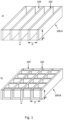
- Fig 1 illustrates an exemplary one-dimensional (1D) X-ray anti-scatter grid module 100-A (in the top part a of Fig. 1 ) and an exemplary two-dimensional (2D) X-ray anti-scatter grid module 100-B (in the bottom part b of Fig. 1 ).
- Each anti-scatter grid module 100 comprises a plurality of X-ray absorbing septa walls 102 separated by interspace material 104.
- the interspace material 104 may be a solid with low X-ray absorption.
- the interspace material may be air or another gas.
- the septa walls 102 are arranged to form an array of grid pixels where p is the grid pixel pitch, h is the septa wall height, and w is the septa wall thickness.
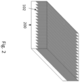
- Fig. 2 shows an example of a 1D grid module, such as a module for a 1D anti-scatter grid or grating.
- the walls 102 are manufactured in a substrate 200, which also acts as supporting carrier for the walls 102.
- Examples of manufacturing technologies for such 1D-modules 100-A (or similar 2D grid modules 100-B) include making gold-filled channels in silicon by RIE (LIGA), tungsten-filled channels made in glass by femto-laser etching etc.
- Fig. 3 schematically shows a micro-device 10, including multiple tiled modules 11, 12, 13, 14.
- the four tiled modules are viewed from above, looking through the first and second covers 106, 108 (not visible in figure).
- Positioning elements 110 are shown as circles in wall cross sections of the device.
- the positioning elements 110 may be protrusions that fit in corresponding recessions in the wall 102 of the module 11, 12.
- the positioning elements 110 may be recessions that fit with protrusions extending from the wall 102.
- Fig. 4 shows a side-view of a micro-structured device including multiple modules 11, 12, sandwiched between two covers 106, 108.
- shock absorbing material 120 such as foam, aerogel, etc.
- the top cover 106 and the bottom cover 108 are mechanically connected to each other with mechanical connections 130 on the outside of the modules 11, 12.
- the covers may be mechanically connected between modules.
- Such mechanical connections provide for improved stability and fixed positions of the modules.
- positioning elements 110 on both covers are in the form of protrusions that extend between modules.
- Fig. 5 illustrates an example of a large 2D grid (2DXL), such as an anti-scatter grid, composed of square 2D grid tiles 11, 12 with square pixels.
- the material of the tiles 11, 12 may be e.g. Tungsten.
- the tiles 11, 12 may be manufactured with 3D printing.
- the tiles 11,12 are merged to create a 2DXL grid without X-ray image artefacts caused by the borders between neighboring tiles.
- Positioning elements 110 in this example consist of protruding pins in the covers 106, 108.
- the pins are shaped accurately to match with grid pixels in the four corners of each 2D grid tile 11, 12.
- the pins stick precisely in the grid pixel openings formed by the (e.g. air-spaced) tungsten septa walls 102.
- Tungsten septa wall 102 thickness may be on the order of 0.1 mm, pin height in the range 0.2-1 mm and grid pixel size in the range 1-3 mm.
- the top part a) of the figure shows the 2DXL grid viewed from the top.
- the bottom part b) illustrates a cross-sectional view A to A'.
- Fig. 6 shows a similar 2DXL grid assembly concept as in Fig. 5 .
- hexagonal 2D grid tiles 11, 12 are joined seamlessly together to form a 2DXL grid.
- the positioning marks 110 at the borders of each tile 11, 12 ensure a well-defined distance between all neighboring grid tiles. This is important to realize a smooth X-ray scatter profile at the tile boundaries. As an example, the gap width between tiles may be ca. 20% of the pixel size.
- the figure illustrates an example including the use of six positioning marks 110 for each 60-degree corner of a hexagonal grid tile 11, 12. Another option is to use three marks 110 positioned in the vertices of an equilateral triangle in the hexagonal tile 11, 12.
- each hexagonal grid tile 11, 12 to use three marks 110 in the bottom cover and additionally three marks 110 in the top cover, as indicated schematically by two equilateral triangles in the top left hexagonal tile.
- the top part a) of the figure shows the 2DXL grid viewed from the top.
- the bottom part b) illustrates a cross-sectional view A to A'.
- Fig. 7 shows a 2DXL grid composed of square 2D grid tiles 11, 12 with square pixels.
- the tiles 11, 12 may be manufactured from glass filled with X-ray absorbing material to form the walls 102.
- the tiles 11. 12 are merged to create a seamless 2DXL grid.
- it may be difficult to apply positioning marks 110 inserted in pixel openings since the space between septa walls 102 may be (partly) filled with a solid material instead of air, and/or pixel sizes are smaller (such as down to 0.2 mm). Therefore, it may preferable, as shown in Fig. 7 , to use protruding ridges 110 in the grid covers 106, 108 to position and align the 2D grid tiles relative to each other.
- Septa wall 102 thickness and height h may be ca. 30 ⁇ m and 2 mm, respectively. Ridge height may in this example be in the range 0.2-1 mm and grid pixel size may be in the range 0.2-0.5 mm.
- the top part a) of the figure shows the 2DXL grid viewed from the top.
- the bottom part b) illustrates a cross-sectional view A to A'.
- Fig. 8 illustrates a 2DXL grid composed of rectangular 2D grid tiles 11, 12 with square pixels. Like in e.g. Fig. 7 , the tiles 11, 12 are merged with a controlled gap, but in this case the tiles 11, 12 are aligned by protruding pins 110 located in the periphery of the grid covers 106, 108 outside the field of view FOV. The pins match 110 with additional holes etched in the four corners of each 2D grid tile 11, 12. The small gap width between neighboring tiles 11, 12 helps to prevent or reduce X-ray image artefacts caused by tiling.
- the top part a) of the figure shows the 2DXL grid viewed from the top.
- the bottom part b) illustrates a cross-sectional view A to A'.
- the material for the top cover 106 and/or bottom cover 108 may be X-ray absorbing material or an X-ray transparent material.
- X-ray absorbing materials such as Tungsten or Molybdenum can be used to add additional X-ray absorbing functionality to the device.
- the absorbing cover may be patterned with the same grid structure matching as the underlying modules.
- the grid modules 11, 12, such as for an anti-scatter grid focusing to the focal spot of an X-ray tube it is possible to use an alignment pattern of at least one cover 106, 108, to ensure that the correct focus module 11, 12 is positioned at the required position, to match with the angles of the walls 102, such as at the center or at the periphery of the micro-structured device.
- the focusing functionality of the stack may be supported by the cover 106, 108 itself, in which case a thicker cover 106, 108 is preferred.
- the modules may be built from glass structuring technologies, such as laser etched glass, made with X-ray or gamma-ray absorbing walls 102.
- At least one of the covers 106, 108 may alternatively or additionally be made from structured glass.
- Such glass a cover 106, 108 may be X-ray and gamma-ray transparent over its entire surface or have X-ray or gamma-ray absorbing structures integrated in a pattern, such as to match or supplement grid functionality of the modules 11, 12.
- top and bottom cover 106, 108 may be connected to each other in a monocoque or semi-monocoque envelope construction, which is advantageous to keep the tiles in stable fixed position relative to each other.
- a surrounding frame such as an aluminum frame, may be used to attach top cover and bottom cover to each other.
- Positioning elements 110 in a cover 106, 108, such as a cover made by from carbon, may be fabricated by subtractive manufacturing (e.g. CNC machining) and/or by additive manufacturing (e.g. casting a stack of carbon laminate foils in a pre-formed negative mold containing the positioning marks).
- the positioning marks 110 may cause small gain variations in acquired X-ray images when located in the field of view, but these can easily be corrected by image preprocessing. Positioning marks 110 may be applied on only one cover or on both covers. In an example, positioning marks may be applied at alternate positions in both covers to minimize local X-ray absorption differences. Depending on the chosen assembly concept and the properties of the grid tiles (material, dimensions, geometry, etc.), the skilled person will appreciate that various other embodiments of positioning marks in the grid covers and combinations with additional alignment features in the grid tiles are conceivable. For example, in Figs. 5 and 6 the grid tiles may be aligned by protruding ridges along the tiles instead of pins inserted in the corners of the tile. In Fig. 7 , the protruding ridges around each glass grid tile may be shortened to only e.g. the corners of the tile. In Fig. 8 , protruding ridges along the grid tiles could be added in the FOV of the grid.
- any reference signs placed between parentheses shall not be construed as limiting the claim.
- the word “comprising” does not exclude the presence of elements or steps other than those listed in a claim.
- the word “a” or “an” preceding an element does not exclude the presence of a plurality of such elements.
- several of these means may be embodied by one and the same item of hardware. Measures recited in mutually different dependent claims may advantageously be used in combination.
Landscapes
- Physics & Mathematics (AREA)
- Spectroscopy & Molecular Physics (AREA)
- Engineering & Computer Science (AREA)
- General Engineering & Computer Science (AREA)
- High Energy & Nuclear Physics (AREA)
- Measurement Of Radiation (AREA)
Abstract
A micro-structured device (10) for selective transmission of radiation comprises a first module (11) and a second module (12). Each of the first module and the second module comprises multiple walls (102) with a height (h). For each of the first module and the second module, the walls (102) form multiple repeating grid units for selective transmission of X-ray and/or gamma-ray radiation.
A first cover (106) on a first side of the first and the second modules extends, transversally to the height (h), over the multiple repeating grid units of the first module (11) and the second module (12). A second cover (108) on a second side of the first and the second modules, the second side being opposite to the first side, extends, transversally to the height (h), over the multiple repeating grid units of the first module (11) and the second module (12).
According to the invention, at least one of the first cover (106) and the second cover (108) comprises a positioning element (110) for aligning the position of the first and/or second module.
Description
- The invention relates to a micro-structured device for selective transmission of radiation.
- Manufacturing of high-performance microstructures for selective transmission of X-ray or gamma-ray radiation, such as X-ray anti-scatter grids for advanced X-ray imaging systems, with a large surface area is challenging, as it requires very accurate and consistent dimensioning and positioning of the thin and high wall structures uniformly over the complete area. There are typically limitations to the size of the manufacturing platforms that can be used, e.g. when manufacturing the microstructures with 3D printing technology. Consequently, manufacturing process yields may be low for 'large area' structures, such as micro-structured devices larger than 20 x 20 cm2. One option to mitigate this challenge is manufacturing of smaller grid tiles and subsequently merging (tiling) multiple such small grid tiles to form a larger structure.
- Schröter et al, J. Phys. D: Appl. Phys. 50 (2017) 225401, describe large-area full field x-ray differential phase-contrast imaging using 2D tiled gratings.
- Possible alignment errors and interfaces between adjacent grid tiles can lead to image artifacts as well as structural instabilities and risk of breakage. Hence, there is a need to improve such 'large area' micro-structured devices.
- It is, inter alia, an object of the invention to provide an improved micro-structured device for selective transmission of radiation. The invention is defined by the independent claims. Advantageous embodiments are defined in the dependent claims.
- According to a first aspect of the invention, there is provided a micro-structured device for selective transmission of radiation. The device comprises:
- a first module and a second module, wherein each of the first module and the second module comprises multiple walls with a height, and wherein for each of the first module and the second module, the walls form multiple repeating grid units for selective transmission of X-ray and/or gamma-ray radiation;
- a first cover on a first side of the first and the second module, wherein the first cover extends, transversally to the height (h), over the multiple repeating grid units of the first module and the second module; and
- a second cover on a second side of the first and the second module, wherein the second side is opposite to the first side, wherein the second cover extends, transversally to the height, over the multiple repeating grid units of the first module and the second module. In accordance with the invention, at least one of the first cover and the second cover comprises a positioning element for aligning the position of the first and/or second module.
- The covers on either side of the modules in combination with the positioning element provide alignment and support to the modules of the micro-structured device. In this way, it is possible to accurately position and keep in place the modules, relative to each other, such that selective transmission of X-ray and/or gamma-ray radiation is achieved across an area of the device that is larger in size than an individual module. Preferably, each of the first cover and the second cover comprises at least one positioning element and/or at least one of the covers comprises multiple positioning elements. With the help of the covers and positioning elements it may be possible to avoid expensive sensors and positioning equipment during assembly to accurately align all modules in the correct positions relative to each other. The positioning elements in the covers may provide for "self-alignment". Furthermore, the invention may prevent a module from being placed in a wrong position, and may simplify correction of a possibly wrongly positioned module. The exact positions of individual modules in a micro-structured device may be of particular importance for structures such as focused grid, where different positions require different angulation of the walls. The covers and positioning elements may prevent module positions from changing during operation in an imaging system (e.g. rotational scan of a C-arm imaging system). Therefore, grid lifetime and/or performance during varying environmental conditions, such as humidity and temperature may be improved.
- Each of the modules has multiple repeating grid units for selective transmission of X-ray and/or gamma-ray radiation. Each of the repeating grid units are of the same or similar size as the other grid units, such as grid units forming multiple similar grid 'pixels' in an anti-scatter grid or grating. All repeating grid units may not be identical. As mentioned above, there may be variations in angulation of the walls between grid units, such as for focused grids where grid pixels are focused towards e.g. one spot and grid pixels at the edges may have different angulation than in the middle of the device.
- The modules are manufactured as separate pieces. Preferably, the modules are free standing structures, such that the micro-structured device can be easily assembled. Each module may be monolithic or may be a composite structure. Examples of ranges for module grid unit parameters may be repeating grid unit pitch (distance between the center of adjacent repeating grid units) between 0.1 and 2 mm, wall thickness between 20-100 µm, and wall height between 2-10 mm. In another example, such as suitable for absorption gratings, the unit pitch may be between 10 and 50 µm, the wall thickness between 5 and 25 µm, and the wall height between 100 and 500 µm.
- The covers may be thin rigid plates or flexible foils. Preferably an average thickness of each cover is less than 10% of the height of the walls of the modules, such as in the range of less than 0.2 - 1 mm for modules with a grid wall height in the range of 2 - 10 mm. The micro-structured device may include more than two modules to further increase the effective area for selective transmission of radiation. Preferably an area of the micro-structured device is larger than 400 cm2, more preferably larger than 1500 cm2.
- According to an embodiment of the invention, the positioning element comprises a cover protrusion and/or a cover recession. Advantageously, at least one of the first module and the second module comprises a module protrusion matched to a cover recession and/or a module recession matched to a cover protrusion. In this way, the positioning element of the cover may connect to a corresponding element of the module, such that the module is kept in place and/or aligned to the cover. A protrusion may be in the form of a wedge, a pyramid, a cone, a stair shape, a pin, a ridge, or similar structures. A corresponding recession would preferably be the 'inverse' of such a protrusion structure. However, dimensions and/or shape may vary to some extent between corresponding protrusions and recessions, e.g. to allow for easier manufacturing, considering variances in dimensions etc. In one example, a recession may be in the form of a slit, 'canyon', or similar, such that a corresponding protrusion, e.g. in the form of a pin or cone or ridge, may move sideways within the recession and/or be slid into the recession from the side.
- According to an embodiment of the invention, the walls of each module comprise at least one high-Z material for attenuation of X-ray and/or gamma-ray radiation. A high-Z material is a material (element) with a high atomic number Z. Such materials provide good absorption of X-ray and gamma-ray radiation, which is advantageous e.g. to absorb scattered radiation through the grid units. The high-Z material is preferably a metal. The high-Z material may preferably be Tungsten (Wolfram, W, with atomic number 74). Other examples of high-Z materials, include Molybdenum (Mo, atomic number 42), Tantalum (Ta, atomic number 73), Niobium (Nb, atomic number 41), Lead (Pb, atomic number 82), Bismuth (Bi, atomic number 83), Rhenium (Re, atomic number 75), Silver (Ag, atomic number 47) and Gold (Au, atomic number 79). The high-Z material preferably has an atomic number Z exceeding 40, and more preferably exceeding 70. The walls may alternatively or additionally or in combination comprise an alloy including at least one high-Z material.
- According to an embodiment of the invention, at least one of the covers comprises a transmission material that is substantially transparent to X-ray and/or gamma-ray radiation, wherein a density of the transmission material is less than 10 g/cm3, preferably less than 5 g/cm3 and more preferably less than 3 g/cm3. In this way, the cover, or the sections of the cover comprising such material, will not interfere with the radiation through the micro-structured device. Examples of such cover materials with large X-ray and/or gamma-ray transparency may include carbon (such as carbon fiber, carbon fiber reinforced composite, etc.), polymer (such as acrylic, polycarbonate, polystyrene, nylon, polyimide, polyethylene, polyester, etc.), aluminum, glass, vulcanized fiber, etc.
- According to an embodiment of the invention, at least one of the covers comprises at least one high-Z material for attenuation of X-ray and/or gamma-ray radiation, wherein the high-Z material forms a wall pattern for radiation attenuating functionality aligned with the grid units of the modules. In this way, the cover may fulfill an additional function of enhancing the function of selective transmission of X-ray and/or gamma-ray radiation through the micro-structured device. The high-Z material may be the same or different to a high-Z material the walls of the module as described above. The wall pattern may alternatively or additionally or in combination comprise an alloy including at least one high-Z material.
- According to an embodiment of the invention, the wall pattern of high-Z material of at least one of the covers comprises tilted walls for providing focused grid functionality. The tilted walls are preferably focused towards one focal point. In this way, the cover may provide for an enhanced focused grid functionality together with the grid structures of the modules.
- According to an embodiment of the invention, the first module and the second module are aligned with the positioning element, such that adjacent sides of the two modules are separated by a gap that on average is larger than zero and smaller than 200% of a pitch of the repeating grid units of each module. Preferably, the gap is on average smaller than 100% of the pitch, and more preferably smaller than 50% of the pitch. In this way a small, controlled distance between the modules may be achieved for improved radiation scatter profile across the interface between the modules. An improved scatter profile may be achieved by avoiding 'double walls' of grid units from two adjacent modules of the device.
- According to an embodiment of the invention, the positioning element comprises a protrusion extending in the gap between the modules in the direction of the height of the modules. In this way, the modules may easily be separated in a controlled way, for an improved scatter profile, with one or several protrusions.
- According to an embodiment of the invention, the first cover and the second cover are mechanically connected to each other between and/or outside of the modules. In this way, the mechanical stability of the micro-structured device may be improved. Furthermore, the connections between the two covers may also function to align and keep in place the modules.
- According to an embodiment of the invention, the device comprises a shock absorbing layer between at least one of the modules and at least one of the covers. In this way, the risk of structural damage during e.g. assembly and/or handling of the micro-structured device may be reduced. A shockabsorbing layer may also help to even out small variations in e.g. height of the modules due to manufacturing variances. Preferably, the shock absorbing layer is substantially transparent to X-ray and/or gamma-ray radiation.
- According to an embodiment of the invention, the device comprises a spacer material between the first module and the second module. Such a spacer material may help to provide improved mechanical stability of the device. The spacer material may prevent modules from moving with respect to each other and reduce risk for mechanical damage. The spacer layer may be substantially transparent to X-ray and/or gamma-ray radiation.
- As previously mentioned, examples of materials with high transparency to X-ray and/or gamma-ray radiation may be materials with a density of less than 10 g/cm3, preferably less than 5 g/cm3 and more preferably less than 3 g/cm3. Examples of such X-ray and/or gamma-ray transparent materials include carbon, polymers, aluminum, glass, vulcanized fiber, cotton fiber, glue, aerogel, foam, paper etc.
- According to a second aspect of the invention, there is provided an imaging component comprising the device according to the first aspect, wherein the imaging component comprises at least one of an X-ray or gamma-ray anti-scatter device; an X-ray or gamma-ray filter; an X-ray or gamma-ray collimator; an X-ray or gamma-ray grating.
- According to a third aspect of the invention, there is provided an imaging system comprising the imaging component according to the second aspect. Such an imaging system may be a computed tomography imaging system, a radiography system, a fluoroscopy system, a cone beam computed tomography system, a C-arm interventional imaging system, a positron emission tomography system, a single-photon emission computerized tomography system etc.
- These and other aspects of the invention will be apparent from and elucidated with reference to the embodiments described hereinafter.
-
-
Fig. 1 schematically illustrates modules with repeating grid units. -
Fig. 2 schematically illustrates another example of a 1D grid module. -
Figs. 3-8 schematically illustrate micro-structured devices comprising multiple modules and top and bottom covers. -
Fig 1 illustrates an exemplary one-dimensional (1D) X-ray anti-scatter grid module 100-A (in the top part a ofFig. 1 ) and an exemplary two-dimensional (2D) X-ray anti-scatter grid module 100-B (in the bottom part b ofFig. 1 ). Eachanti-scatter grid module 100 comprises a plurality of X-ray absorbingsepta walls 102 separated byinterspace material 104. Theinterspace material 104 may be a solid with low X-ray absorption. The interspace material may be air or another gas. Thesepta walls 102 are arranged to form an array of grid pixels where p is the grid pixel pitch, h is the septa wall height, and w is the septa wall thickness. -
Fig. 2 shows an example of a 1D grid module, such as a module for a 1D anti-scatter grid or grating. In this example, thewalls 102 are manufactured in asubstrate 200, which also acts as supporting carrier for thewalls 102. Examples of manufacturing technologies for such 1D-modules 100-A (or similar 2D grid modules 100-B) include making gold-filled channels in silicon by RIE (LIGA), tungsten-filled channels made in glass by femto-laser etching etc. -
Fig. 3 schematically shows a micro-device 10, including multipletiled modules second covers 106, 108 (not visible in figure). Positioningelements 110 are shown as circles in wall cross sections of the device. Thepositioning elements 110 may be protrusions that fit in corresponding recessions in thewall 102 of themodule positioning elements 110 may be recessions that fit with protrusions extending from thewall 102. -
Fig. 4 shows a side-view of a micro-structured device includingmultiple modules covers grid tiles covers Fig. 4 , thetop cover 106 and thebottom cover 108 are mechanically connected to each other withmechanical connections 130 on the outside of themodules Fig. 4 ,positioning elements 110 on both covers are in the form of protrusions that extend between modules. -
Fig. 5 illustrates an example of a large 2D grid (2DXL), such as an anti-scatter grid, composed of square2D grid tiles tiles tiles tiles elements 110 in this example consist of protruding pins in thecovers 2D grid tile tungsten septa walls 102. Across the 2DXL grid area the shape of the pins may be angulated and or tapered towards the top for optimal fit with the focused grid tiles.Tungsten septa wall 102 thickness may be on the order of 0.1 mm, pin height in the range 0.2-1 mm and grid pixel size in the range 1-3 mm. The top part a) of the figure shows the 2DXL grid viewed from the top. The bottom part b) illustrates a cross-sectional view A to A'. -
Fig. 6 . shows a similar 2DXL grid assembly concept as inFig. 5 . In this case hexagonal2D grid tiles tile positioning marks 110 for each 60-degree corner of ahexagonal grid tile marks 110 positioned in the vertices of an equilateral triangle in thehexagonal tile hexagonal grid tile marks 110 in the bottom cover and additionally threemarks 110 in the top cover, as indicated schematically by two equilateral triangles in the top left hexagonal tile. The top part a) of the figure shows the 2DXL grid viewed from the top. The bottom part b) illustrates a cross-sectional view A to A'. -
Fig. 7 shows a 2DXL grid composed of square2D grid tiles tiles walls 102. Thetiles 11. 12 are merged to create a seamless 2DXL grid. With some manufacturing technologies, it may be difficult to applypositioning marks 110 inserted in pixel openings, since the space betweensepta walls 102 may be (partly) filled with a solid material instead of air, and/or pixel sizes are smaller (such as down to 0.2 mm). Therefore, it may preferable, as shown inFig. 7 , to use protrudingridges 110 in the grid covers 106, 108 to position and align the 2D grid tiles relative to each other.Septa wall 102 thickness and height h may be ca. 30 µm and 2 mm, respectively. Ridge height may in this example be in the range 0.2-1 mm and grid pixel size may be in the range 0.2-0.5 mm. The top part a) of the figure shows the 2DXL grid viewed from the top. The bottom part b) illustrates a cross-sectional view A to A'. -
Fig. 8 illustrates a 2DXL grid composed of rectangular2D grid tiles Fig. 7 , thetiles tiles pins 110 located in the periphery of the grid covers 106, 108 outside the field of view FOV. The pins match 110 with additional holes etched in the four corners of each2D grid tile tiles - It should be noted that the above-mentioned embodiments illustrate rather than limit the invention, and that those skilled in the art will be able to design many alternative embodiments without departing from the scope of the appended claims. As non-limiting examples, the material for the
top cover 106 and/orbottom cover 108 may be X-ray absorbing material or an X-ray transparent material. X-ray absorbing materials such as Tungsten or Molybdenum can be used to add additional X-ray absorbing functionality to the device. In such an example, the absorbing cover may be patterned with the same grid structure matching as the underlying modules. For 2D focusing design of thegrid modules cover correct focus module walls 102, such as at the center or at the periphery of the micro-structured device. The focusing functionality of the stack may be supported by thecover thicker cover ray absorbing walls 102. At least one of thecovers cover modules - The top and
bottom cover elements 110 in acover Figs. 5 and6 the grid tiles may be aligned by protruding ridges along the tiles instead of pins inserted in the corners of the tile. InFig. 7 , the protruding ridges around each glass grid tile may be shortened to only e.g. the corners of the tile. InFig. 8 , protruding ridges along the grid tiles could be added in the FOV of the grid. - In the claims, any reference signs placed between parentheses shall not be construed as limiting the claim. The word "comprising" does not exclude the presence of elements or steps other than those listed in a claim. The word "a" or "an" preceding an element does not exclude the presence of a plurality of such elements. In the device claim enumerating several means, several of these means may be embodied by one and the same item of hardware. Measures recited in mutually different dependent claims may advantageously be used in combination.
Claims (15)
- A micro-structured device (10) for selective transmission of radiation, the device comprising:a first module (11) and a second module (12), wherein each of the first module and the second module comprises multiple walls (102) with a height (h), and wherein for each of the first module and the second module, the walls (102) form multiple repeating grid units for selective transmission of X-ray and/or gamma-ray radiation;a first cover (106) on a first side of the first and the second modules, wherein the first cover (106) extends, transversally to the height (h), over the multiple repeating grid units of the first module (11) and the second module (12); anda second cover (108) on a second side of the first and the second modules, wherein the second side is opposite to the first side, wherein the second cover extends, transversally to the height (h), over the multiple repeating grid units of the first module (11) and the second module (12),wherein at least one of the first cover (106) and the second cover (108) comprises a positioning element (110) for aligning the position of the first and/or second module.
- The device according to claim 1, wherein the positioning element (110) comprises a cover protrusion and/or a cover recession.
- The device according to claim 2, wherein at least one of the first module (11) and the second module (12) comprises a module protrusion matched to a cover recession and/or a module recession matched to a cover protrusion.
- The device according to any of the previous claims, wherein the walls (102) of each module (11, 12) comprise at least one high-Z material for attenuation of X-ray and/or gamma-ray radiation, such as one or more of Tungsten, Molybdenum, Tantalum, Niobium, Lead, Bismuth, Rhenium, Silver, and Gold.
- The device according to any of the preceding claims, wherein at least one of the covers (106, 108) comprises a transmission material that is substantially transparent to X-ray and/or gamma-ray radiation, wherein a density of the transmission material is less than 10 g/cm3, preferably less than 5 g/cm3 and more preferably less than 3 g/cm3.
- The device according to claim 5, wherein the transmission material comprises at least one of carbon, polymer, aluminum, glass, and vulcanized fiber.
- The device according to any of the preceding claims, wherein at least one of the covers (106, 108) comprises at least one high-Z material for attenuation of X-ray and/or gamma-ray radiation, such as one or more of Tungsten, Molybdenum, Tantalum, Niobium, Lead, Bismuth, Rhenium, Silver, and Gold, and wherein the high-Z material forms a wall pattern for radiation attenuating functionality aligned with the grid units of the modules.
- The device according to claim 7, wherein the wall pattern of high-Z material of at least one of the covers (106, 108) comprises tilted walls for providing focused grid functionality, and wherein the tilted walls are preferably focused towards one focal point.
- The device according to any of the preceding claims, wherein the first module (11) and the second module (12) are aligned with the positioning element (110), such that adjacent sides of the modules are separated by a gap that on average is larger than zero and smaller than 200% of a pitch of the repeating grid units of each module.
- The device according to claim 9, wherein the positioning element (110) comprises a protrusion extending in the gap between the modules in the direction of the height (h) of the modules.
- The device according to any of the preceding claims, wherein the first cover (106) and the second cover (108) are mechanically connected to each other between and/or outside of the modules.
- The device according to any of the preceding claims, wherein the device comprises a shock absorbing layer (120) between at least one of the modules (11, 12) and at least one of the covers (106, 108).
- The device according to any of the preceding claims, wherein the device comprises a spacer material between the first module (11) and the second module (12).
- An imaging component comprising the device according to any of the preceding claims, wherein the imaging component comprises at least one of:an X-ray or gamma-ray anti-scatter device;an X-ray or gamma-ray filter;an X-ray or gamma-ray collimator;an X-ray or gamma-ray grating.
- An imaging system comprising the imaging component according to claim 14.
Priority Applications (2)
| Application Number | Priority Date | Filing Date | Title |
|---|---|---|---|
| EP23205427.0A EP4546374A1 (en) | 2023-10-24 | 2023-10-24 | Micro-structured device for selective transmission of radiation |
| PCT/EP2024/079873 WO2025087933A1 (en) | 2023-10-24 | 2024-10-23 | Imaging component comprising flat anti-scatter grid |
Applications Claiming Priority (1)
| Application Number | Priority Date | Filing Date | Title |
|---|---|---|---|
| EP23205427.0A EP4546374A1 (en) | 2023-10-24 | 2023-10-24 | Micro-structured device for selective transmission of radiation |
Publications (1)
| Publication Number | Publication Date |
|---|---|
| EP4546374A1 true EP4546374A1 (en) | 2025-04-30 |
Family
ID=88511040
Family Applications (1)
| Application Number | Title | Priority Date | Filing Date |
|---|---|---|---|
| EP23205427.0A Withdrawn EP4546374A1 (en) | 2023-10-24 | 2023-10-24 | Micro-structured device for selective transmission of radiation |
Country Status (2)
| Country | Link |
|---|---|
| EP (1) | EP4546374A1 (en) |
| WO (1) | WO2025087933A1 (en) |
Citations (5)
| Publication number | Priority date | Publication date | Assignee | Title |
|---|---|---|---|---|
| US20020064252A1 (en) * | 2000-11-27 | 2002-05-30 | Kenji Igarashi | Detector unit, X-ray computer tomographic photographing device, X-ray detector, and X-ray detector manufacturing method |
| US20040057556A1 (en) * | 2002-09-20 | 2004-03-25 | Koninklijke Philips Electronics N.V. | Method and apparatus for alignment of anti-scatter grids for computed tomography detector arrays |
| US20060227930A1 (en) * | 2003-07-22 | 2006-10-12 | Mattson Rodney A | Radiation mask for two dimensional ct detector |
| US20120069954A1 (en) * | 2010-09-22 | 2012-03-22 | Toshiba Medical Systems Corporation | X-ray computed tomography apparatus, radiation detector, and method of manufacturing radiation detector |
| US20170097423A1 (en) * | 2014-05-26 | 2017-04-06 | General Electric Company | Radiation Detection Apparatus and Radiation Tomography Apparatus |
Family Cites Families (1)
| Publication number | Priority date | Publication date | Assignee | Title |
|---|---|---|---|---|
| EP4011293A1 (en) | 2020-12-14 | 2022-06-15 | Koninklijke Philips N.V. | X-ray imaging systems for reducing artefacts associated with anti-scatter grids and methods of operating the same. |
-
2023
- 2023-10-24 EP EP23205427.0A patent/EP4546374A1/en not_active Withdrawn
-
2024
- 2024-10-23 WO PCT/EP2024/079873 patent/WO2025087933A1/en active Pending
Patent Citations (5)
| Publication number | Priority date | Publication date | Assignee | Title |
|---|---|---|---|---|
| US20020064252A1 (en) * | 2000-11-27 | 2002-05-30 | Kenji Igarashi | Detector unit, X-ray computer tomographic photographing device, X-ray detector, and X-ray detector manufacturing method |
| US20040057556A1 (en) * | 2002-09-20 | 2004-03-25 | Koninklijke Philips Electronics N.V. | Method and apparatus for alignment of anti-scatter grids for computed tomography detector arrays |
| US20060227930A1 (en) * | 2003-07-22 | 2006-10-12 | Mattson Rodney A | Radiation mask for two dimensional ct detector |
| US20120069954A1 (en) * | 2010-09-22 | 2012-03-22 | Toshiba Medical Systems Corporation | X-ray computed tomography apparatus, radiation detector, and method of manufacturing radiation detector |
| US20170097423A1 (en) * | 2014-05-26 | 2017-04-06 | General Electric Company | Radiation Detection Apparatus and Radiation Tomography Apparatus |
Non-Patent Citations (1)
| Title |
|---|
| SCHROTER ET AL., J. PHYS. D: APPL. PHYS, vol. 50, 2017, pages 225401 |
Also Published As
| Publication number | Publication date |
|---|---|
| WO2025087933A1 (en) | 2025-05-01 |
Similar Documents
| Publication | Publication Date | Title |
|---|---|---|
| US6661012B2 (en) | X-ray detector | |
| US6839408B2 (en) | Two-dimensional, anti-scatter grid and collimator designs, and its motion, fabrication and assembly | |
| JP5674507B2 (en) | Two-dimensional collimator module, X-ray detector, X-ray CT apparatus, two-dimensional collimator module assembling method, and two-dimensional collimator apparatus manufacturing method. | |
| JP6384588B2 (en) | X-ray detector | |
| US20070064878A1 (en) | Antiscatter grid having a cell-like structure of radiation channels, and method for producing such an antiscatter grid | |
| US6304626B1 (en) | Two-dimensional array type of X-ray detector and computerized tomography apparatus | |
| CN111407299B (en) | X-ray collimator, X-ray detector system and CT equipment | |
| US7615161B2 (en) | Simplified way to manufacture a low cost cast type collimator assembly | |
| EP2694999B1 (en) | Imaging detector | |
| US20100171038A1 (en) | Sensor unit for an x-ray detector and associated production method | |
| JP2008510131A (en) | Arrangement of scintillator and anti-scatter grid | |
| EP4546374A1 (en) | Micro-structured device for selective transmission of radiation | |
| JP5943758B2 (en) | Collimator module, radiation detection apparatus, and radiation tomography apparatus | |
| US20050111627A1 (en) | Method of shielding scattered radiation in front of a detector array | |
| WO2017102831A1 (en) | Radiation detector with an anti-scatter grid | |
| JP2024026391A (en) | X-ray detector with focused scintillator structure for uniform imaging | |
| EP1927999B1 (en) | Method of manufacturing an X-ray CT system | |
| EP4517390A1 (en) | Self contained ct scintillators within a 3-d printed collimator | |
| WO2000021096A1 (en) | Beam hardening filter for x-ray source | |
| JP2001296366A (en) | Two-dimensional array type radiation detector | |
| CN118105102A (en) | Anti-scatter grid with stop element and sensor element stacked arrangement | |
| JPH11276469A (en) | X-ray CT detector |
Legal Events
| Date | Code | Title | Description |
|---|---|---|---|
| PUAI | Public reference made under article 153(3) epc to a published international application that has entered the european phase |
Free format text: ORIGINAL CODE: 0009012 |
|
| STAA | Information on the status of an ep patent application or granted ep patent |
Free format text: STATUS: THE APPLICATION HAS BEEN PUBLISHED |
|
| AK | Designated contracting states |
Kind code of ref document: A1 Designated state(s): AL AT BE BG CH CY CZ DE DK EE ES FI FR GB GR HR HU IE IS IT LI LT LU LV MC ME MK MT NL NO PL PT RO RS SE SI SK SM TR |
|
| STAA | Information on the status of an ep patent application or granted ep patent |
Free format text: STATUS: THE APPLICATION IS DEEMED TO BE WITHDRAWN |
|
| 18D | Application deemed to be withdrawn |
Effective date: 20251031 |