EP4546329A1 - Display device and method of driving the same - Google Patents
Display device and method of driving the same Download PDFInfo
- Publication number
- EP4546329A1 EP4546329A1 EP24206144.8A EP24206144A EP4546329A1 EP 4546329 A1 EP4546329 A1 EP 4546329A1 EP 24206144 A EP24206144 A EP 24206144A EP 4546329 A1 EP4546329 A1 EP 4546329A1
- Authority
- EP
- European Patent Office
- Prior art keywords
- emission control
- control signal
- active area
- width
- luminance
- Prior art date
- Legal status (The legal status is an assumption and is not a legal conclusion. Google has not performed a legal analysis and makes no representation as to the accuracy of the status listed.)
- Pending
Links
Images








Classifications
-
- G—PHYSICS
- G09—EDUCATION; CRYPTOGRAPHY; DISPLAY; ADVERTISING; SEALS
- G09G—ARRANGEMENTS OR CIRCUITS FOR CONTROL OF INDICATING DEVICES USING STATIC MEANS TO PRESENT VARIABLE INFORMATION
- G09G3/00—Control arrangements or circuits, of interest only in connection with visual indicators other than cathode-ray tubes
- G09G3/20—Control arrangements or circuits, of interest only in connection with visual indicators other than cathode-ray tubes for presentation of an assembly of a number of characters, e.g. a page, by composing the assembly by combination of individual elements arranged in a matrix no fixed position being assigned to or needed to be assigned to the individual characters or partial characters
- G09G3/22—Control arrangements or circuits, of interest only in connection with visual indicators other than cathode-ray tubes for presentation of an assembly of a number of characters, e.g. a page, by composing the assembly by combination of individual elements arranged in a matrix no fixed position being assigned to or needed to be assigned to the individual characters or partial characters using controlled light sources
- G09G3/30—Control arrangements or circuits, of interest only in connection with visual indicators other than cathode-ray tubes for presentation of an assembly of a number of characters, e.g. a page, by composing the assembly by combination of individual elements arranged in a matrix no fixed position being assigned to or needed to be assigned to the individual characters or partial characters using controlled light sources using electroluminescent panels
- G09G3/32—Control arrangements or circuits, of interest only in connection with visual indicators other than cathode-ray tubes for presentation of an assembly of a number of characters, e.g. a page, by composing the assembly by combination of individual elements arranged in a matrix no fixed position being assigned to or needed to be assigned to the individual characters or partial characters using controlled light sources using electroluminescent panels semiconductive, e.g. using light-emitting diodes [LED]
- G09G3/3208—Control arrangements or circuits, of interest only in connection with visual indicators other than cathode-ray tubes for presentation of an assembly of a number of characters, e.g. a page, by composing the assembly by combination of individual elements arranged in a matrix no fixed position being assigned to or needed to be assigned to the individual characters or partial characters using controlled light sources using electroluminescent panels semiconductive, e.g. using light-emitting diodes [LED] organic, e.g. using organic light-emitting diodes [OLED]
- G09G3/3266—Details of drivers for scan electrodes
-
- G—PHYSICS
- G09—EDUCATION; CRYPTOGRAPHY; DISPLAY; ADVERTISING; SEALS
- G09G—ARRANGEMENTS OR CIRCUITS FOR CONTROL OF INDICATING DEVICES USING STATIC MEANS TO PRESENT VARIABLE INFORMATION
- G09G3/00—Control arrangements or circuits, of interest only in connection with visual indicators other than cathode-ray tubes
- G09G3/20—Control arrangements or circuits, of interest only in connection with visual indicators other than cathode-ray tubes for presentation of an assembly of a number of characters, e.g. a page, by composing the assembly by combination of individual elements arranged in a matrix no fixed position being assigned to or needed to be assigned to the individual characters or partial characters
- G09G3/2092—Details of a display terminals using a flat panel, the details relating to the control arrangement of the display terminal and to the interfaces thereto
-
- G—PHYSICS
- G09—EDUCATION; CRYPTOGRAPHY; DISPLAY; ADVERTISING; SEALS
- G09G—ARRANGEMENTS OR CIRCUITS FOR CONTROL OF INDICATING DEVICES USING STATIC MEANS TO PRESENT VARIABLE INFORMATION
- G09G3/00—Control arrangements or circuits, of interest only in connection with visual indicators other than cathode-ray tubes
- G09G3/20—Control arrangements or circuits, of interest only in connection with visual indicators other than cathode-ray tubes for presentation of an assembly of a number of characters, e.g. a page, by composing the assembly by combination of individual elements arranged in a matrix no fixed position being assigned to or needed to be assigned to the individual characters or partial characters
- G09G3/22—Control arrangements or circuits, of interest only in connection with visual indicators other than cathode-ray tubes for presentation of an assembly of a number of characters, e.g. a page, by composing the assembly by combination of individual elements arranged in a matrix no fixed position being assigned to or needed to be assigned to the individual characters or partial characters using controlled light sources
- G09G3/30—Control arrangements or circuits, of interest only in connection with visual indicators other than cathode-ray tubes for presentation of an assembly of a number of characters, e.g. a page, by composing the assembly by combination of individual elements arranged in a matrix no fixed position being assigned to or needed to be assigned to the individual characters or partial characters using controlled light sources using electroluminescent panels
-
- G—PHYSICS
- G09—EDUCATION; CRYPTOGRAPHY; DISPLAY; ADVERTISING; SEALS
- G09G—ARRANGEMENTS OR CIRCUITS FOR CONTROL OF INDICATING DEVICES USING STATIC MEANS TO PRESENT VARIABLE INFORMATION
- G09G3/00—Control arrangements or circuits, of interest only in connection with visual indicators other than cathode-ray tubes
- G09G3/20—Control arrangements or circuits, of interest only in connection with visual indicators other than cathode-ray tubes for presentation of an assembly of a number of characters, e.g. a page, by composing the assembly by combination of individual elements arranged in a matrix no fixed position being assigned to or needed to be assigned to the individual characters or partial characters
- G09G3/34—Control arrangements or circuits, of interest only in connection with visual indicators other than cathode-ray tubes for presentation of an assembly of a number of characters, e.g. a page, by composing the assembly by combination of individual elements arranged in a matrix no fixed position being assigned to or needed to be assigned to the individual characters or partial characters by control of light from an independent source
- G09G3/36—Control arrangements or circuits, of interest only in connection with visual indicators other than cathode-ray tubes for presentation of an assembly of a number of characters, e.g. a page, by composing the assembly by combination of individual elements arranged in a matrix no fixed position being assigned to or needed to be assigned to the individual characters or partial characters by control of light from an independent source using liquid crystals
-
- G—PHYSICS
- G09—EDUCATION; CRYPTOGRAPHY; DISPLAY; ADVERTISING; SEALS
- G09G—ARRANGEMENTS OR CIRCUITS FOR CONTROL OF INDICATING DEVICES USING STATIC MEANS TO PRESENT VARIABLE INFORMATION
- G09G3/00—Control arrangements or circuits, of interest only in connection with visual indicators other than cathode-ray tubes
- G09G3/20—Control arrangements or circuits, of interest only in connection with visual indicators other than cathode-ray tubes for presentation of an assembly of a number of characters, e.g. a page, by composing the assembly by combination of individual elements arranged in a matrix no fixed position being assigned to or needed to be assigned to the individual characters or partial characters
- G09G3/34—Control arrangements or circuits, of interest only in connection with visual indicators other than cathode-ray tubes for presentation of an assembly of a number of characters, e.g. a page, by composing the assembly by combination of individual elements arranged in a matrix no fixed position being assigned to or needed to be assigned to the individual characters or partial characters by control of light from an independent source
- G09G3/36—Control arrangements or circuits, of interest only in connection with visual indicators other than cathode-ray tubes for presentation of an assembly of a number of characters, e.g. a page, by composing the assembly by combination of individual elements arranged in a matrix no fixed position being assigned to or needed to be assigned to the individual characters or partial characters by control of light from an independent source using liquid crystals
- G09G3/3611—Control of matrices with row and column drivers
- G09G3/3674—Details of drivers for scan electrodes
-
- G—PHYSICS
- G09—EDUCATION; CRYPTOGRAPHY; DISPLAY; ADVERTISING; SEALS
- G09G—ARRANGEMENTS OR CIRCUITS FOR CONTROL OF INDICATING DEVICES USING STATIC MEANS TO PRESENT VARIABLE INFORMATION
- G09G2300/00—Aspects of the constitution of display devices
- G09G2300/08—Active matrix structure, i.e. with use of active elements, inclusive of non-linear two terminal elements, in the pixels together with light emitting or modulating elements
- G09G2300/0809—Several active elements per pixel in active matrix panels
- G09G2300/0819—Several active elements per pixel in active matrix panels used for counteracting undesired variations, e.g. feedback or autozeroing
-
- G—PHYSICS
- G09—EDUCATION; CRYPTOGRAPHY; DISPLAY; ADVERTISING; SEALS
- G09G—ARRANGEMENTS OR CIRCUITS FOR CONTROL OF INDICATING DEVICES USING STATIC MEANS TO PRESENT VARIABLE INFORMATION
- G09G2300/00—Aspects of the constitution of display devices
- G09G2300/08—Active matrix structure, i.e. with use of active elements, inclusive of non-linear two terminal elements, in the pixels together with light emitting or modulating elements
- G09G2300/0809—Several active elements per pixel in active matrix panels
- G09G2300/0842—Several active elements per pixel in active matrix panels forming a memory circuit, e.g. a dynamic memory with one capacitor
-
- G—PHYSICS
- G09—EDUCATION; CRYPTOGRAPHY; DISPLAY; ADVERTISING; SEALS
- G09G—ARRANGEMENTS OR CIRCUITS FOR CONTROL OF INDICATING DEVICES USING STATIC MEANS TO PRESENT VARIABLE INFORMATION
- G09G2300/00—Aspects of the constitution of display devices
- G09G2300/08—Active matrix structure, i.e. with use of active elements, inclusive of non-linear two terminal elements, in the pixels together with light emitting or modulating elements
- G09G2300/0809—Several active elements per pixel in active matrix panels
- G09G2300/0842—Several active elements per pixel in active matrix panels forming a memory circuit, e.g. a dynamic memory with one capacitor
- G09G2300/0861—Several active elements per pixel in active matrix panels forming a memory circuit, e.g. a dynamic memory with one capacitor with additional control of the display period without amending the charge stored in a pixel memory, e.g. by means of additional select electrodes
-
- G—PHYSICS
- G09—EDUCATION; CRYPTOGRAPHY; DISPLAY; ADVERTISING; SEALS
- G09G—ARRANGEMENTS OR CIRCUITS FOR CONTROL OF INDICATING DEVICES USING STATIC MEANS TO PRESENT VARIABLE INFORMATION
- G09G2310/00—Command of the display device
- G09G2310/02—Addressing, scanning or driving the display screen or processing steps related thereto
- G09G2310/0243—Details of the generation of driving signals
-
- G—PHYSICS
- G09—EDUCATION; CRYPTOGRAPHY; DISPLAY; ADVERTISING; SEALS
- G09G—ARRANGEMENTS OR CIRCUITS FOR CONTROL OF INDICATING DEVICES USING STATIC MEANS TO PRESENT VARIABLE INFORMATION
- G09G2310/00—Command of the display device
- G09G2310/02—Addressing, scanning or driving the display screen or processing steps related thereto
- G09G2310/0264—Details of driving circuits
-
- G—PHYSICS
- G09—EDUCATION; CRYPTOGRAPHY; DISPLAY; ADVERTISING; SEALS
- G09G—ARRANGEMENTS OR CIRCUITS FOR CONTROL OF INDICATING DEVICES USING STATIC MEANS TO PRESENT VARIABLE INFORMATION
- G09G2310/00—Command of the display device
- G09G2310/02—Addressing, scanning or driving the display screen or processing steps related thereto
- G09G2310/0264—Details of driving circuits
- G09G2310/0267—Details of drivers for scan electrodes, other than drivers for liquid crystal, plasma or OLED displays
-
- G—PHYSICS
- G09—EDUCATION; CRYPTOGRAPHY; DISPLAY; ADVERTISING; SEALS
- G09G—ARRANGEMENTS OR CIRCUITS FOR CONTROL OF INDICATING DEVICES USING STATIC MEANS TO PRESENT VARIABLE INFORMATION
- G09G2310/00—Command of the display device
- G09G2310/06—Details of flat display driving waveforms
- G09G2310/067—Special waveforms for scanning, where no circuit details of the gate driver are given
-
- G—PHYSICS
- G09—EDUCATION; CRYPTOGRAPHY; DISPLAY; ADVERTISING; SEALS
- G09G—ARRANGEMENTS OR CIRCUITS FOR CONTROL OF INDICATING DEVICES USING STATIC MEANS TO PRESENT VARIABLE INFORMATION
- G09G2310/00—Command of the display device
- G09G2310/08—Details of timing specific for flat panels, other than clock recovery
-
- G—PHYSICS
- G09—EDUCATION; CRYPTOGRAPHY; DISPLAY; ADVERTISING; SEALS
- G09G—ARRANGEMENTS OR CIRCUITS FOR CONTROL OF INDICATING DEVICES USING STATIC MEANS TO PRESENT VARIABLE INFORMATION
- G09G2320/00—Control of display operating conditions
- G09G2320/02—Improving the quality of display appearance
- G09G2320/0233—Improving the luminance or brightness uniformity across the screen
-
- G—PHYSICS
- G09—EDUCATION; CRYPTOGRAPHY; DISPLAY; ADVERTISING; SEALS
- G09G—ARRANGEMENTS OR CIRCUITS FOR CONTROL OF INDICATING DEVICES USING STATIC MEANS TO PRESENT VARIABLE INFORMATION
- G09G2320/00—Control of display operating conditions
- G09G2320/02—Improving the quality of display appearance
- G09G2320/0247—Flicker reduction other than flicker reduction circuits used for single beam cathode-ray tubes
-
- G—PHYSICS
- G09—EDUCATION; CRYPTOGRAPHY; DISPLAY; ADVERTISING; SEALS
- G09G—ARRANGEMENTS OR CIRCUITS FOR CONTROL OF INDICATING DEVICES USING STATIC MEANS TO PRESENT VARIABLE INFORMATION
- G09G2340/00—Aspects of display data processing
- G09G2340/04—Changes in size, position or resolution of an image
- G09G2340/0407—Resolution change, inclusive of the use of different resolutions for different screen areas
- G09G2340/0435—Change or adaptation of the frame rate of the video stream
-
- G—PHYSICS
- G09—EDUCATION; CRYPTOGRAPHY; DISPLAY; ADVERTISING; SEALS
- G09G—ARRANGEMENTS OR CIRCUITS FOR CONTROL OF INDICATING DEVICES USING STATIC MEANS TO PRESENT VARIABLE INFORMATION
- G09G2360/00—Aspects of the architecture of display systems
- G09G2360/16—Calculation or use of calculated indices related to luminance levels in display data
-
- G—PHYSICS
- G09—EDUCATION; CRYPTOGRAPHY; DISPLAY; ADVERTISING; SEALS
- G09G—ARRANGEMENTS OR CIRCUITS FOR CONTROL OF INDICATING DEVICES USING STATIC MEANS TO PRESENT VARIABLE INFORMATION
- G09G3/00—Control arrangements or circuits, of interest only in connection with visual indicators other than cathode-ray tubes
- G09G3/20—Control arrangements or circuits, of interest only in connection with visual indicators other than cathode-ray tubes for presentation of an assembly of a number of characters, e.g. a page, by composing the assembly by combination of individual elements arranged in a matrix no fixed position being assigned to or needed to be assigned to the individual characters or partial characters
- G09G3/22—Control arrangements or circuits, of interest only in connection with visual indicators other than cathode-ray tubes for presentation of an assembly of a number of characters, e.g. a page, by composing the assembly by combination of individual elements arranged in a matrix no fixed position being assigned to or needed to be assigned to the individual characters or partial characters using controlled light sources
- G09G3/30—Control arrangements or circuits, of interest only in connection with visual indicators other than cathode-ray tubes for presentation of an assembly of a number of characters, e.g. a page, by composing the assembly by combination of individual elements arranged in a matrix no fixed position being assigned to or needed to be assigned to the individual characters or partial characters using controlled light sources using electroluminescent panels
- G09G3/32—Control arrangements or circuits, of interest only in connection with visual indicators other than cathode-ray tubes for presentation of an assembly of a number of characters, e.g. a page, by composing the assembly by combination of individual elements arranged in a matrix no fixed position being assigned to or needed to be assigned to the individual characters or partial characters using controlled light sources using electroluminescent panels semiconductive, e.g. using light-emitting diodes [LED]
- G09G3/3208—Control arrangements or circuits, of interest only in connection with visual indicators other than cathode-ray tubes for presentation of an assembly of a number of characters, e.g. a page, by composing the assembly by combination of individual elements arranged in a matrix no fixed position being assigned to or needed to be assigned to the individual characters or partial characters using controlled light sources using electroluminescent panels semiconductive, e.g. using light-emitting diodes [LED] organic, e.g. using organic light-emitting diodes [OLED]
- G09G3/3225—Control arrangements or circuits, of interest only in connection with visual indicators other than cathode-ray tubes for presentation of an assembly of a number of characters, e.g. a page, by composing the assembly by combination of individual elements arranged in a matrix no fixed position being assigned to or needed to be assigned to the individual characters or partial characters using controlled light sources using electroluminescent panels semiconductive, e.g. using light-emitting diodes [LED] organic, e.g. using organic light-emitting diodes [OLED] using an active matrix
- G09G3/3233—Control arrangements or circuits, of interest only in connection with visual indicators other than cathode-ray tubes for presentation of an assembly of a number of characters, e.g. a page, by composing the assembly by combination of individual elements arranged in a matrix no fixed position being assigned to or needed to be assigned to the individual characters or partial characters using controlled light sources using electroluminescent panels semiconductive, e.g. using light-emitting diodes [LED] organic, e.g. using organic light-emitting diodes [OLED] using an active matrix with pixel circuitry controlling the current through the light-emitting element
Definitions
- the disclosure generally relates to a display device and a method of driving the same.
- display devices such as a liquid crystal display device and an organic light-emitting display device are increasingly used.
- a high-speed driving function of providing users with images changed at a high frame frequency and a low-speed driving function of providing users with images changed at a low frame frequency are desired in recent display devices.
- a method capable of providing images with similar luminances and minimizing flickers when a display device is driven at a high frequency and a low frequency is desired.
- Embodiments provide a display device and a method of driving the same, which may minimize a luminance difference in one frame.
- Embodiments also provide a display device and a method of driving the same, which may minimize a luminance difference when the display device is driven at a relatively high frequency and a relatively low frequency.
- a display device including: pixels each connected to a corresponding scan line among scan lines, a corresponding data line among data lines, and a corresponding emission control line among emission control lines; and an emission driver which supplies an emission control signal to the emission control lines, where the emission control signal includes a first emission control signal having a first width and at least one second emission control signal having a second width during an active area of one frame.
- the emission driver may supply the first emission control signal during a writing period in which a data signal is supplied to the pixels in the active area, and supply the second emission control signal during a period except the writing period in the active area.
- the second width may be set as a relatively wide width as compared with the first width.
- the emission driver may further supply a third emission control signal having a third width during the period except the writing period in the active area.
- the third width may be set as a relatively wide width as compared with the first width, and the second width and the third width may be set as widths equal to or different from each other.
- the second emission control signal may be supplied as a second active area emission control signal in the active area
- the third emission control signal may be supplied as a fourth active area emission control signal in the active area
- the second emission control signal may be supplied as a second active area emission control signal in the active area
- the third emission control signal may be supplied as a third active area emission control signal in the active area
- the display device may further include a timing controller which controls the emission driver.
- the timing controller may include a storage unit in which information of the first width, the second width, and the third width is stored.
- the timing controller may further include a luminance determiner which determines a luminance in a unit of the one frame, corresponding to input data.
- the timing controller may change positions at which the second emission control signal and the third emission control signal are supplied, corresponding to the luminance.
- the timing controller may supply the second emission control signal as a second active area emission control signal in the active area, and supply the third emission control signal as a third emission control signal in the active area.
- the timing controller may supply the second emission control signal as a third active area emission control signal in the active area, and supply the third emission control signal as a fourth active area emission control signal in the active area.
- the timing controller may change widths of the second emission control signal and the third emission control signal, corresponding to the luminance.
- the timing controller may increase the widths of the second emission control signal and the third emission control signal when the luminance of the one frame is determined as a relatively high luminance, and decrease the widths of the second emission control signal and the third emission control signal when the luminance of the one frame is determined as a relatively low luminance.
- the second width may be set as a width narrower than the first width, and the emission driver may supply the first emission control signal in a predetermined cycle during an active area and a blank area of one frame.
- the display device may further include a timing controller which controls the emission driver, and the timing controller may change a position at which the second emission control signal is supplied in a unit of at least one frame.
- a method of driving a display device including a pixel of which emission time is controlled corresponding to an emission control signal including: supplying an emission control signal having a first width and an emission control signal having a second width different from the first width during an active area of one frame; and supplying the emission control signal having the first width during a blank area of the one frame.
- the second width may be set as a relatively wide width as compared with the first width.
- a length of the second width may be changed corresponding to a luminance of the one frame.
- the emission control signal having the first width may be supplied in a predetermined cycle in the active area and the blank area.
- the second width may be set as a width narrower than the first width, and a position at which the emission control signal having the second width is supplied may be changed in a unit of at least one frame.
- the expression “equal” may mean “substantially equal.” That is, this may mean equality to a degree to which those skilled in the art may understand the equality.
- Other expressions may be expressions in which "substantially' is omitted.
- each block, each unit, and/or each module may be implemented by dedicated hardware or by a combination dedicated hardware to perform some functions of the block, the unit, and/or the module and a processor (e.g., one or more programmed microprocessors and associated circuitry) to perform other functions of the block, the unit, and/or the module.
- the blocks, the units, and/or the modules may be physically separated into two or more individual blocks, two or more individual units, and/or two or more individual modules without departing from the scope of the disclosure.
- the blocks, the units, and/or the modules may be physically separated into more complex blocks, more complex units, and/or more complex modules without departing from the scope of the disclosure.
- connection between two components may include both electrical connection and physical connection, but the disclosure is not necessarily limited thereto.
- connection used based on circuit diagrams may mean electrical connection
- connection used based on cross-sectional and plan views may mean physical connection.
- FIG. 1 is a diagram illustrating an embodiment of a display device in accordance with the disclosure.
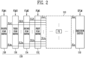
- FIG. 2 is a diagram illustrating an embodiment of a scan driver and an emission driver, which are shown in FIG. 1 .
- the display device 100 in the embodiment of the disclosure includes pixels PX each electrically connected to a corresponding scan line among a plurality of scan lines, a corresponding data line among a plurality of data lines, and a corresponding and a corresponding emission control line among a plurality of emission control lines.
- the display device 100 may include a pixel unit 110 (or panel), a timing controller 120, a scan driver 130, a data driver 140, an emission driver 150, and a power supply 160.
- the disclosure is not restricted to the display device 100 according to FIGS. 1 and 2 and other display devices 100 can be used to implement the concepts of the present disclosure.
- the display device 100 may display an image at various image refresh rates (e.g., driving frequencies or screen refresh rates) according to driving conditions.
- the image refresh rate means a frequency at which a data signal is written to a driving transistor of a pixel PX.
- the image refresh rate may also be referred to as a screen scan rate or a screen refresh frequency, and represent a frequency at which a display screen is reproduced for one second, for example.
- an output frequency of the data driver 140 with respect to one horizontal line may be sorted as one horizontal line (or pixel row)
- an output frequency of a second scan driver 134 which outputs a second scan signal (or writing scan signal) may be determined corresponding to the image refresh rate.
- an image refresh rate for driving a moving image may be a frequency of about 60 hertz (Hz) or higher (e.g., about 120 Hz, about 240 Hz, or the like), for example.
- the display device 100 may display an image, corresponding to various image refresh rates of about 1 Hz to about 240 Hz, for example. However, this is merely illustrative, and the display device 100 may also display an image at an image refresh rate of about 240 Hz or higher (e.g., about 480 Hz).
- the pixel unit 110 may include pixels PX connected to first scan lines SL11, SL12, ..., and SL1n, second scan lines SL21, SL22, ..., and SL2n, third scan lines SL31, SL32, ..., and SL3n, fourth scan lines SL41, SL42, ..., and SL4n, data lines DL1, DL2, ..., and DLm, emission control lines EL1, EL2, ..., and ELo, and power lines PL1, PL2, PL3, ,PL4 and PL5(n, m, and o are natural numbers of 2 or more).
- a pixel PXij (refer to FIG. 3 as a suitable example but the invention is not restricted thereto and other circuits for pixels may be implemented) disposed on an ith horizontal line (or pixel row) and a jth vertical line (or pixel column) may be connected to an ith first scan line SL1i, an ith second scan line SL2i, an ith third scan line SL3i, an ith fourth scan line SL4i, a kth emission control line ELk, and a jth data line DLj (i is an integer of n or less, j is an integer of m or less, and k is an integer of o or less).
- k is a natural number which is equal to i or is smaller than i.
- k when each of the emission control lines EL1 to ELo is connected to pixels PX disposed on one horizontal line, k may be a natural number equal to i. In an embodiment, when each of the emission control lines EL1 to ELo is connected to pixels PX disposed on at least two horizontal lines, k may be a natural number smaller than i.
- the pixels PX may be selected in units of horizontal lines when an enable first scan signal is supplied to the first scan lines SL11 to SL1n, and each of the pixels PX selected by the enable first scan signal may be supplied with a data signal from a data line (any one of DL1 to DLm) connected thereto.
- the pixel PX supplied with the data signal may generate light with a predetermined luminance, corresponding to a voltage of the data signal.
- the scan driver 130 may receive a scan driving signal SCS from the timing controller 120. At least one scan start signal and clock signals, which are desired for driving of the scan driver 130, may be included in the scan driving signal SCS.
- the scan driver 130 may generate the enable first scan signal, an enable second scan signal, an enable third scan signal, and an enable fourth scan signal while shifting the scan start signal, corresponding to the clock signal.
- the scan driver 130 may include a first scan driver 132, the second scan driver 134, a third scan driver 136, and a fourth scan driver 138 as shown in FIG. 2 . At least some of the scan drivers 132, 134, 136, and 138 may be integrated into one driving circuit, one module, or the like according to a design.
- the first scan driver 132 may receive a first scan start signal FLM1, and generate the enable first scan signal while shifting the first scan start signal FLM1, corresponding to the clock signal.
- the first scan driver 132 may sequentially supply the enable first scan signal to the first scan lines SL11 to SL1n.
- the first scan driver 132 may supply the enable first scan signal during a writing period in an active area of one frame.
- the second scan driver 134 may receive a second scan start signal FLM2, and generate the enable second scan signal while shifting the second scan start signal FLM2, corresponding to the clock signal.
- the second scan driver 134 may sequentially supply the enable second scan signal to the second scan lines SL21 to SL2n.
- the second scan driver 134 may supply the enable second scan signal during the writing period in the active area of the one frame.
- the third scan driver 136 may receive a third scan start signal FLM3, and generate the enable third scan signal while shifting the third scan start signal FLM3, corresponding to the clock signal.
- the third scan driver 136 may sequentially supply the enable third scan signal to the third scan lines SL31 to SL3n.
- the third scan driver 136 may supply the enable third scan signal during the writing period in the active area of the one frame.
- the fourth scan driver 138 may receive a fourth scan start signal FLM4, and generate the enable fourth scan signal while shifting the fourth scan start signal FLM4, corresponding to the clock signal.
- the fourth scan driver 138 may sequentially supply the enable fourth scan signal to the fourth scan lines SL41 to SL4n.
- the fourth scan driver 138 may supply the enable fourth scan signal during the writing period in the active area of the one frame.
- the fourth scan driver 138 may supply the enable fourth scan signal during a maintenance period included in the active area and a blank area of the one frame.
- the fourth scan driver 138 may perform scanning once during the writing period of the one frame (i.e., supply at least one enable fourth scan signal), and perform scanning at least once according to the image refresh rate during the maintenance period of the one frame, for example.
- the image refresh rate is decreased (i.e., when a frame length is lengthened)
- the blank area of the one frame is lengthened, and hence a number of maintenance periods included in the blank area may be increased. That is, when the image refresh rate is decreased, a number of times an operation of supplying the enable fourth scan signal is repeated may be increased.
- Each of the enable first scan signal, the enable second scan signal, the enable third scan signal, and the enable fourth scan signal may be set to a gate-on voltage such that transistors included in the pixels PX may be turned on.
- each of an enable first scan signal GW, an enable second scan signal GC, an enable third scan signal GI, and an enable fourth scan signal GB, which are supplied to a P-type transistor as shown in FIG. 3 may be set to a relatively low level voltage.
- the first scan driver 132, the second scan driver 134, the third scan driver 136, and the fourth scan driver 138 are respectively connected to a first scan line SL1, a second scan line SL2, a third scan line SL3, and a fourth scan line SL4.
- the disclosure is not limited thereto.
- at least two scan lines (at least two of SL1, SL2, SL3, and SL4) among the first scan line SL1, the second scan line SL2, the third scan line SL3, and the fourth scan line SL4 may be driven by one scan driver.
- the data driver 140 may receive output data Dout and a data driving signal DCS from the timing controller 120.
- the data driving signal DCS may include a sampling signal and/or timing signals, desired for driving of the data driver 140.
- the data driver 140 may generate a data signal, based on the data driving signal DCS and the output data Dout. In an embodiment, the data driver 140 may generate an analog data signal, based on a grayscale of the output data Dout.
- the data driver 140 may supply the data signal in one horizontal period unit.
- the emission driver 150 may receive an emission driving signal ECS from the timing controller 120.
- An emission start signal and clock signals, which are desired for driving the emission driver 150, may be included in the emission driving signal ECS.
- the emission driver 150 may generate a disable emission control signal (or relatively high level emission control signal) EM (refer to FIG. 3 ) while shifting the emission start signal, corresponding to the clock signal.
- the emission driver 150 may receive an emission start signal EFLM, and generate the disable emission control signal EM while shifting the emission start signal EFLM, corresponding to the clock signal.
- the emission driver 150 may sequentially supply the disable emission control signal EM to the emission control lines EL1 to ELo.
- the disable emission control signal EM may be set to a gate-off voltage such that the transistors included in the pixels PX may be turned off.
- the disable emission control signal EM supplied to the P-type transistor as shown in FIG. 3 may be set to a relatively high level voltage.
- the emission driver 150 may supply the disable emission control signal EM during the writing period and the maintenance period of the one frame. In an embodiment, the emission driver 150 may perform scanning once during the writing period of the one frame, and perform scanning at least once according to the image refresh rate during the maintenance period of the one frame, for example.
- the image refresh rate is decreased (i.e., when the frame length is lengthened)
- the blank area of the one frame is lengthened, and hence the number of maintenance periods included in the blank area may be increased. That is, when the image refresh rate is decreased, a number of times an operation of supplying the disable emission control signal EM is repeated may be increased.
- the timing controller 120 may receive input data Din and a control signal CS from a host system through an interface.
- the timing controller 120 may receive the input data Din and the control signal CS from at least one of a graphics processing unit ("GPU”), a central processing unit (“CPU”), and an application processor ("AP"), which are included in the host system.
- Various signals including a clock signal may be included in the control signal CS.
- the timing controller 120 may generate the scan driving signal SCS, the data driving signal DCS, and the emission driving signal ECS, based on the control signal CS.
- the scan driving signal SCS, the data driving signal DCS, and the emission driving signal ECS may be supplied to the scan driver 130, the data driver 140, and the emission driver 150, respectively.
- the timing controller 120 may realign the input data Din to be suitable for specifications of the display device 100. Also, the timing controller 120 may generate the output data Dout by correcting the input data Din, and supply the output data Dout to the data driver 140. In an embodiment, the timing controller 120 may correct the input data Din, corresponding to an optical measurement result measured in a processing process.
- the power supply 160 may generate various power sources desired for driving of the display device 100.
- the power supply 160 may generate a first driving power source VDD, a second driving power source VSS, a first initialization power source Vint1, a second initialization power source Vint2, and a bias power source Vbias.
- the first driving power source VDD may be a power source which supplies a driving current to the pixels PX.
- the second driving power source VSS may be a power source which is supplied with the driving current from the pixels PX.
- the first driving power source VDD may be set to a voltage higher than a voltage of the second driving power source VSS during a period in which the pixels PX is set to be in an emission state.
- the first initialization power source Vint1 may be a power source for initializing a gate electrode a driving transistor included in each of the pixels PX.
- the first initialization power source Vint1 may be set to a voltage lower than a voltage of the data signal.
- the second initialization power source Vint2 may be a power source for initializing a first electrode (or anode electrode) of a light-emitting element LD (refer to FIG. 3 ) included in each of the pixels PX.
- the second initialization power source Vint2 may be set to a voltage at which the light-emitting element LD is turned off.
- the bias power source Vbias may be a power source for applying an on-bias voltage to the driving transistor included in each of the pixels PX.
- the first driving power source VDD generated by the power supply 160 may be supplied to a first power line PL1, the second driving power source VSS generated by the power supply 160 may be supplied to a second power line PL2, the first initialization power source Vint1 generated by the power supply 160 may be supplied to a third power line PL3, the second initialization power source Vint2 generated by the power supply 160 may be supplied to a fourth power line PL4, and the bias power source Vbias generated by the power supply 160 may be supplied to a fifth power line PL5.
- the first power line PL1, the second power line PL2, the third power line PL3, the fourth power line PL4, and the fifth power line PL5 may be commonly connected to the pixels PX, but the disclosure is not limited thereto.
- the first power line PL1 may be configured with a plurality of power lines, and the plurality of power lines may be connected to different pixels PX.
- the second power line PL2 may be configured with a plurality of power lines, and the plurality of power lines may be connected to different pixels PX.
- the third power line PL3 may be configured with a plurality of power lines, and the plurality of power lines may be connected to different pixels PX.
- the fourth power line PL4 may be configured with a plurality of power lines, and the plurality of power lines may be connected to different pixels PX.
- the fifth power line PL5 may be configured with a plurality of power lines, and the plurality of power lines may be connected to different pixels PX. That is, in an embodiment of the disclosure, the pixels PX may be connected to any one of the plurality of power lines of the first power line PL1, any one of the plurality of power lines of the second power line PL2, any one of the plurality of power lines of the third power line PL3, any one of the plurality of power lines of the fourth power line PL4, and any one of the plurality of power lines of the fifth power line PL5.
- the display device 100 may include a flat display device, a curved display device in which a portion of the pixel unit 110 is curved, a flexible display device in which a portion of the pixel unit 110 is folded or bent, and a stretchable display device in which a portion of the pixel unit 110 is expanded/contracted.
- the display device is a device which displays moving images or still images, and may include portable electronic devices such as a mobile phone, a smartphone, a tablet personal computer ("PC"), a smart watch, a watch phone, a portable multimedia player ("PMP"), a navigation system, and an ultra mobile computer (“UMPC”).
- the display device 100 may include electronic devices such as a television, a notebook computer, a monitor, an advertisement board, and Internet of things (“IoT").
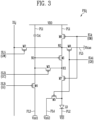
- FIG. 3 is a diagram illustrating an embodiment of a pixel in accordance with the disclosure.
- a pixel PXij disposed on an ith horizontal line and a jth vertical line will be illustrated.
- the disclosure is not restricted to the circuit of the pixel according to FIG. 3 and other circuitry may be used to implement the concepts of the present disclosure.
- the pixel PXij in the embodiment of the disclosure may be connected to corresponding signal lines SL1i, SL2i, SL3i, SL4i, ELk, and DLj.
- the pixel PXij may be connected to an ith first scan line SL1i, an ith second scan line SL2i, an ith third scan line SL3i, an ith fourth scan line SL4i, a kth emission control line ELk, and a jth data line DLj, for example.
- the pixel PXij may be further connected to the first power line PL1, the second power line PL2, the third power line PL3, the fourth power line PL4, and the fifth power line PL5.
- the pixel PXij in the embodiment of the disclosure may include a light-emitting element LD and a pixel circuit for controlling an amount of current supplied to the light-emitting element LD.
- the light-emitting element LD may be connected between the first power line PL1 and the second power line PL2.
- a first electrode (or anode electrode) of the light-emitting element LD may be electrically connected to the first power line PL1 via a seventh transistor M7, a third node N3, a first transistor M1, a second node N2, and a sixth transistor M6, and a second electrode (or cathode electrode) of the light-emitting element LD may be electrically connected to the second power line PL2.
- the light-emitting element LD may generate light with a predetermined luminance, corresponding to an amount of current supplied from the first power line PL1 to the second power line PL2 via the pixel circuit.
- the light-emitting element LD may be selected as an organic light-emitting diode ("OLED"). Also, the light-emitting element LD may be selected as an inorganic light-emitting diode (“LED”) such as a micro LED or a quantum dot LED. Also, the light-emitting element LD may be an element configured with a combination of an organic material and an inorganic material.
- OLED organic light-emitting diode
- LED inorganic light-emitting diode
- the light-emitting element LD may be an element configured with a combination of an organic material and an inorganic material.
- FIG. 3 it is illustrated that the pixel PXij includes a single light-emitting element LD. However, in another embodiment, the pixel PXij may include a plurality of light-emitting elements LD, and the plurality of light-emitting elements LD may be connected in series, parallel or series/parallel to each other.
- the pixel circuit may include the first transistor M1, a second transistor M2, a third transistor M3, a fourth transistor M4, a fifth transistor M5, the sixth transistor M6, the seventh transistor M7, an eighth transistor M8, and a storage capacitor Cst.
- a first electrode of the first transistor M1 (or driving transistor) may be connected to the second node N2, and a second electrode of the first transistor M1 may be connected to the third node N3.
- a gate electrode of the first transistor M1 may be connected to a first node N1.
- the first transistor M1 may control an amount of current supplied from the first driving power source VDD to the second driving power source VSS via the light-emitting element LD, corresponding to a voltage of the first node N1.
- the second transistor M2 may be connected between the j-th data line DLj and the second node N2.
- a gate electrode of the second transistor M2 may be electrically connected to the first scan line SL1i.
- the second transistor M2 may be turned on when an enable first scan signal GW is supplied to the second scan line SL2i, to electrically connect the j-th data line DLj and the second node N2 to each other.
- the third transistor M3 may be connected between the first node N1 and the third node N3.
- a gate electrode of the third transistor M3 may be electrically connected to the second scan line SL2i.
- the third transistor M3 may be turned on when an enable second scan signal GC is supplied to the second scan line SL2i, to electrically connect the first node N1 and the third node N3 to each other. That is, when the third transistor M3 is turned on, the first transistor M1 may be connected in a diode form.
- a first electrode of the fourth transistor M4 may be connected to the first node N1, and a second electrode of the fourth transistor M4 may be electrically connected to the third power line PL3.
- a gate electrode of the fourth transistor M4 may be electrically connected to the third scan line SL3i.
- the fourth transistor M4 may be turned on when an enable third scan signal GI is supplied to the third scan line SL3i, to supply the voltage of the first initialization power source Vint1 to the first node N1.
- a first electrode of the fifth transistor M5 may be electrically connected to the first electrode of the light-emitting element LD, and a second electrode of the fifth transistor M5 may be electrically connected to the fourth power line PL4.
- a gate electrode of the fifth transistor M5 may be electrically connected to the fourth scan line SL4i.
- the fifth transistor M5 may be turned off when an enable fourth scan signal GB is supplied to the fourth scan line SL4i, to supply the voltage of the second initialization power source Vint2 to the first electrode of the light-emitting element LD.
- a parasitic capacitor of the light-emitting element LD may be discharged.
- a residual voltage charged in the parasitic capacitor of the light-emitting element LD is discharged (or removed), unintended minute emission may be prevented.
- the black expression ability of the pixel PXij may be improved.
- a first electrode of the sixth transistor M6 may be electrically connected to the first power line PL1, and a second electrode of the sixth transistor M6 may be connected to the second node N2.
- a gate electrode of the sixth transistor M6 may be electrically connected to the kth emission control line ELk.
- the sixth transistor M6 may be turned off when a disable emission control signal EM is supplied to the kth emission control line ELk, and be turned on when an enable emission control signal EM is supplied to the kth emission control line ELk.
- the seventh transistor M7 may be connected between the third node N3 and the first electrode of the light-emitting element LD.
- a gate electrode of the seventh transistor M7 may be electrically connected to the kth emission control line ELk.
- the seventh transistor M7 may be turned off when the disable emission control signal EM is supplied to the kth emission control line ELk, and be turned on when the enable emission control signal EM is supplied to the kth emission control line ELk.
- a first electrode of the eighth transistor M8 (or bias transistor) may be electrically connected to the fifth power line PL5, and a second electrode of the eighth transistor M8 may be connected to the second node N2.
- a gate electrode of the eighth transistor M8 may be electrically connected to the fourth scan line SL4i.
- the eighth transistor M8 may be turned on when the enable fourth scan signal GB is supplied to the fourth scan line SL4i, to electrically connect the fifth power line PL5 and the second node N2 to each other.
- the storage capacitor Cst may be connected between the first power line PL1 and the first node N1.
- the storage capacitor Cst may store a voltage applied to the first node N1.
- the first to eighth transistors M1 to M8 are implemented with a P-type transistor.
- the disclosure is not limited thereto.
- Some transistors (e.g., M3 and M4) among the first to eighth transistors M1 to M8 may be implemented with an N-type transistor.
- FIG. 4 is a waveform diagram illustrating an embodiment of a method of driving the pixel shown in FIG. 3 during a writing period.
- the writing period WP may be included in an active area of a frame.
- the writing period WP may include a first period P1, a second period P2, a third period P3, and a fourth period P4.
- the first period P1 to the third period P3 may be set as a non-emission period
- the fourth period P4 may be set as an emission period.
- the disable emission control signal EM may be supplied to the kth emission control line ELk.
- the sixth transistor M6 and the seventh transistor M7 may be turned off.
- the sixth transistor M6 and the seventh transistor M7 are turned off, electric connection between the first power line PL1 and the light-emitting element LD may be blocked, and accordingly, the light-emitting element LD may be set to be in a non-emission state.
- the enable third scan signal GI may be supplied to the third scan line SL3i.
- the fourth transistor M4 may be turned on.
- the voltage of the first initialization power source Vint1 of the third power line PL3 may be supplied to the first node N1.
- the voltage of the first initialization power source Vint1 is supplied to the first node N1, may be set to be in a strong on-bias state.
- the enable second scan signal GC may be supplied to the second scan line SL2i, and accordingly, the third transistor M3 may be turned on.
- the third transistor M3 When the third transistor M3 is turned on, the first transistor M1 may be diode-connected.
- the enable first scan signal GW may be supplied to the first scan line SL1i.
- the second transistor M2 may be turned on.
- a data signal from the j-th data line DLj may be supplied to the second node N2. Since the form in which the first transistor M1 is diode-connected is maintained by the turned-on third transistor M3, the first node N1 may have a voltage obtained by compensating for a threshold voltage of the first transistor M1 in the data signal.
- the enable fourth scan signal GB may be supplied to the fourth scan line SL4i.
- the fifth transistor M5 and the eighth transistor M8 may be turned on.
- the voltage of the second initialization power source Vint2 may be supplied to the first electrode of the light-emitting element LD, and accordingly, the light-emitting element LD may be initialized.
- the eighth transistor M8 is turned on, a voltage of the bias power source Vbias may be supplied to the second node N2.
- the first transistor M1 may be set to be in an on-bias state.
- the enable emission control signal (or relatively low level emission control signal) EM may be supplied to the kth emission control line ELk, so that the sixth transistor M6 and the seventh transistor M7 are turned on.
- a current flowing path may be formed from the first power line PL1 to the second power line PL2 via the sixth transistor M6, the first transistor M1, the seventh transistor M7, and the light-emitting element LD.
- a driving current corresponding to the voltage of the first node N1 may flow through the light-emitting element LD according to an operation of the first transistor M1, and the light-emitting element LD may emit light with a luminance corresponding to the driving current.
- FIG. 5 is a waveform diagram illustrating an embodiment of the method of driving the pixel shown in FIG. 3 during a maintenance period.
- the waveform diagram may refer to the embodiments of the display device 100 of FIGS. 1 and 2 and/or the pixel described in FIG. 3 but is not restricted thereto. The diagram may also apply to other display devices 100 and pixels PX different to the ones described as examples in FIGS. 1 , 2 and 3 .
- the maintenance period MP is a period in which light is emitted while maintaining the voltage of a data signal supplied previously, and may be a period in which an image is displayed without changing any frame.
- one frame may include one writing period WP in an active area thereof and a plurality of maintenance periods MP in the active area and a blank area thereof. The plurality of maintenance periods MP may be successively disposed after the writing period WP.
- the maintenance period MP As compared with the writing period WP, in the maintenance period MP, a threshold voltage compensation operation and a data writing operation may be omitted, and an operation of applying a bias voltage to the first transistor M1 and an operation of initializing the light-emitting element LD may be performed.
- the maintenance period MP may be set to have a length similar to a length of the writing period WP.
- the maintenance period MP may include a first period P1a, a second period P2a, a third period P3a, and a fourth period P4a.
- the disable emission control signal EM may be supplied to the kth emission control line ELk.
- the sixth transistor M6 and the seventh transistor M7 may be turned off, and accordingly, the light-emitting element LD may be set to be in the non-emission state.
- the enable first scan signal GW, the enable second scan signal GC, and the enable third scan signal GI may not be supplied (or disable scan signals GW, GC, and GI may be supplied). Accordingly, in the first period P1a to the third period P3a, the second transistor M2, the third transistor M3, and the fourth transistor M4 may be set to be in a turn-off state.
- the enable fourth scan signal GB may be supplied to the fourth scan line SL4i.
- the fifth transistor M5 and the eighth transistor M8 may be turned on.
- the above-described display device 100 in the embodiment of the disclosure may be driven at various driving frequencies (various frame frequencies).
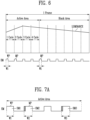
- FIG. 6 is a diagram illustrating a luminance of one frame period according to a comparative example.
- the diagram may refer to the embodiments of the display device 100 of FIGS. 1 and 2 and/or the pixel described in FIG. 3 but is not restricted thereto.
- the diagram may also apply to other display devices 100 and pixels PX different to the ones described as examples in FIGS. 1 and 2 .
- a luminance of pixels disposed on one horizontal line will be illustrated.
- a portion indicated by Cycle may mean a period in which light the pixels emit and do not emit light in response to one emission control signal EM.
- FIG. 6 it is assumed that the display device 100 is driven at about 48 Hz, and ten disable emission control signals EM are supplied during one frame period.
- four disable emission control signals (also referred to as first to fourth active area emission control signals, respectively) EM may be supplied in an active area Active Area.
- the active area Active Area may include one writing period WP and three maintenance periods MP.
- the active area Active Area may be set to have the same length regardless of the image refresh rate, and accordingly, the number (e.g., 4) of disable emission control signals EM supplied in the active area Active Area may be set constant regardless of the image refresh rate.
- six disable emission control signals EM may be supplied in a blank are Blank Area.
- the blank are Blank Area may include six maintenance periods MP.
- the length of the blank area Blank Area may be differently set corresponding to the image refresh rate, and accordingly, the number of disable emission control signals EM supplied in the blank area Blank Area may be differently set corresponding to the image refresh rate.
- the luminance of a predetermined horizontal line may be increased during a predetermined period and then be continuously decreased.
- the luminance of the predetermined horizontal line may be increased during periods 1 Cycle and 2 Cycle of the active area Active Area, and be gradually decreased after a start point of a period 3 Cycle.
- the first transistor M1 may be set to be in the strong on-bias state during the first period P1 of the writing period WP as described in FIG. 4 .
- a characteristic curve of the first transistor M1 may be changed (e.g., negative shift), and the luminance of the predetermined horizontal line may be gradually increased while the characteristic curve of the first transistor M1 returns to the original place during a predetermined period (e.g., the periods 1 Cycle and 2 Cycle) (e.g., the luminance of the predetermined horizontal lien may be gradually increased during the periods 1 Cycle and 2 Cycle).
- the luminance of the predetermined horizontal line may be gradually decreased by a leakage current of the third transistor M3 and the fourth transistor M4.
- the width of disable emission control signals EM supplied in the active area Active Area may be controlled so as to minimize the luminance difference on the predetermined horizontal line.
- FIGS. 7A and 7B are diagram illustrating an embodiment of emission control signals supplied during the active area.
- the luminance of a predetermined horizontal line may be set highest the period 3 Cycle during the one frame period.
- the luminance difference of the predetermined horizontal line may be minimized, and accordingly, display quality may be improved.
- a luminance difference from a blank area Blank Area of a previous frame may occur.
- the luminance difference between the previous frame and the current frame is minimized, and accordingly, the display quality may be improved.
- At least two disable emission control signals EM having different widths are supplied in the active area Active Area.
- a disable emission control signal EM which may be supplied in a writing period WP of the active area Active Area, set to have a first width W1.
- the disable emission control signal EM having the first width W1 may be also referred to as a first emission control signal EM1.
- a disable emission control signal having the first width W1 may also be supplied in a maintenance period MP of the blank area Blank Area.
- At least one disable emission control signal which is included in the active area Active Area which may be supplied in the maintenance period MP after the writing period WP, has a width different from the first width W1.
- a second disable emission control signal EM2 supplied in the active area Active Area (or supplied in a first maintenance period MP) is set to have a second width W2.
- the disable emission control signal EM having the second width W2 may be also referred to as a second emission control signal EM2.
- a fourth disable emission control signal EM supplied in the active area Active Area may be set to have a third width W3.
- the disable emission control signal EM having the third width W3 may be also referred to as a third emission control signal EM3.
- Each of the second width W2 and the third width W3 may be set as a relatively wide (or long) width, e.g. wider width, as compared with the first width W1. Also, the second width W2 and the third width W3 may be equal to or different from each other.
- a portion hatched by black in the disable emission control signal EM may mean a widened width (or period) as compared with the disable emission control signal EM having the first width W1.
- the second disable emission control signal EM supplied in the active area Active Area is set to have the second width W2 according to the above width relations, an initial luminance of the active area Active Area is decreased, and accordingly, the luminance difference from the blank area Blank Area of the previous frame may be minimized.
- the fourth disable emission control signal EM supplied in the active area Active Area is set to have the third width W3 according to the above width relations, the luminance of the period 3 Cycle is decreased, and accordingly, a luminance difference in the one frame may be minimized.
- FIG. 7A it has been described that the width of the second disable emission control signal EM and the fourth disable emission control signal EM, which are supplied in the active area Active Area, are widened.
- the disclosure is not limited thereto.
- the widths of the second disable emission control signal EM and a third disable emission control signal EM, which are supplied in the active area Active Area may be set relatively wide as shown in FIG. 7B .
- the width of the third disable emission control signal EM is set as the third width W3
- the luminance of the period 2 Cycle and/or the period 3 Cycle is decreased, and accordingly, the luminance difference in the one frame may be minimized.
- FIG. 8 is a diagram illustrating an embodiment of the timing controller shown in FIG. 1 .
- FIG. 8 only components desired for description of the disclosure will be illustrated.
- the timing controller 120 may include a storage unit (e.g., memory) 122.
- Information of the first width W1, the second width W2, and/or the third width W3, which are shown in FIGS. 6 to 7B may be stored in the storage unit 122.
- the first width W1, the second width W2, and/or the third width W3, which are stored in the storage unit 122 may correspond to the width (length, time) of the disable emission control signal.
- the timing controller 120 may supply an emission start signal EFLM having the first width W1 during the writing period WP (or corresponding to the first emission control signal of the frame). Then, the emission driver 150 may supply a disable emission control signal EM having the first width W1 to the emission control lines EL1 to ELo.
- the timing controller 120 may supply an emission start signal EFLM having the second width W2, corresponding to the second disable emission control signal EM. Then, the emission driver 150 may supply a disable emission control signal EM having the second width W2 to the emission control lines EL1 to ELo.
- the timing controller 120 may supply an emission start signal EFLM having the third width W3, corresponding to the fourth disable emission control signal EM. Then, the emission driver 150 may supply a disable emission control signal EM having the third width W3 to the emission control lines EL1 to ELo.
- the timing controller 120 may supply the emission start signal EFLM, corresponding to the third disable emission control signal EM and the other disable emission control signals EM supplied in the blank area Blank Area. Then, the emission driver 150 may supply the disable emission control signal EM having the first width W1 to the emission control lines EL1 to ELo.
- the luminance difference in the one frame may be minimized by the setting the widths, for example, as shown in the embodiments and as described above with respect to FIGS. 7A and 7B .
- FIG. 9 is a diagram illustrating a luminance of one frame period of display devices.
- different display devices are driven at about 48 Hz, and ten disable emission control signals EM are supplied during one frame period.
- the display devices may have different luminances during the one frame period.
- the second width W2 and/or the third width W3, which are shown in FIGS. 7A and 7B may be set to be different with respect to the display devices.
- the second width W2 and the third width W3 are set to be the same for each display device, a characteristic of the display device cannot be reflected. Therefore, in an embodiment of the disclosure, the second width W2 and the third width W3 may be set by reflecting the characteristic of the display device.
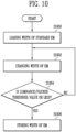
- FIG. 10 is a diagram illustrating an embodiment of an embodiment of a method of setting a width of an emission control signal in accordance with the disclosure.
- the setting of the width of the emission control signal which is shown in FIG. 10 , may be set for each display device 100 through multi-time programming ("MTP").
- MTP multi-time programming
- the width of the emission control signal may be set in a processing process.
- a width of a standard disable emission control signal EM may be loaded (S1000).
- the width of the standard disable emission control signal EM may be set as a first width W1.
- the width of the standard disable emission control signal EM may be loaded by the timing controller 120.
- the width of the standard disable emission control signal EM may be pre-stored in the storage unit 122.
- the width of the standard disable emission control signal EM may be disposed by a separate processing device electrically connected to the timing controller 120 in the processing process.
- a width of at least one disable emission control signal among a second emission control signal EM to a fourth disable emission control signal EM, which are supplied in an active area Active Area may be changed (S1002).
- the width of each of the second disable emission control signal EM (or EM2) and the fourth disable emission control signal EM (or EM3) may be changed as shown in FIG. 7A .
- the width of each of the second disable emission control signal EM (or EM2) and the third disable emission control signal EM (or EM3) may be changed as shown in FIG. 7B .
- the luminance may mean a luminance difference between frames, which corresponds to a change in image refresh rate.
- the flicker may mean a luminance difference in one frame.
- the width of a corresponding disable emission control signal EM may be stored in the storage unit 122 (S1006).
- the operations S1000 to S1004 may be repeated.
- FIG. 11 is a diagram illustrating flicker characteristics of an embodiment of the disclosure and a comparative example.
- a flicker may mean a luminance difference corresponding to a lapse of time in one frame.
- a flicker characteristic obtained by inspecting ten display devices is illustrated.
- a value (or threshold value) satisfying the flicker characteristic may be -60 decibels (dB) or less.
- EMBODIMENT may mean a case where the width of each of the second disable emission control signal EM and the fourth disable emission control signal EM, which are supplied in the active area Active Area, is set to be different as shown, for example, in FIG. 7A and 7B with respect to the display devices.
- "COMPARATIVE EXAMPLE” may mean a case where widths of disable emission control signals EM supplied in the active area Active Area are all set to be the same as shown, for example, in FIG. 6 .
- the flicker characteristic of the display devices may be set to the threshold value or less. That is, in the display devices in the embodiment of the disclosure, a luminance difference in one frame period may be minimized, and accordingly, display quality may be improved.
- a flicker characteristic of some of the display devices of the comparative example may exceed the threshold value.
- the flicker characteristic exceeds the threshold value a luminance difference in one frame period may be recognized by a user.
- the flicker characteristic exceeds the threshold value the display devices may be determined as defective products, and therefore, manufacturing cost may be increased.
- FIG. 12 is a diagram illustrating luminance difference characteristics of an embodiment of the disclosure and a comparative example.
- a luminance difference may mean a luminance difference between frames, which corresponds to a change in image refresh.
- a luminance difference characteristic obtained by inspecting ten display devices is illustrated.
- a value (or threshold value) satisfying the luminance difference characteristic may be about 0.030 nit per hertz (nit/Hz) or less.
- EMBODIMENT may mean a case where the width of each of the second disable emission control signal EM and the fourth disable emission control signal EM, which are supplied in the active area Active Area, is set to be different with respect to the display devices.
- "COMPARATIVE EXAMPLE” may mean a case where widths of disable emission control signals EM supplied in the active area Active Area are all set to be the same.
- the luminance difference characteristic of the display devices may be set to the threshold value or less. That is, the display devices in the embodiment of the disclosure may generate similar luminances in each frame regardless of the change in image refresh rate, and accordingly, display quality may be improved.
- a luminance difference characteristic of some of the display devices of the comparative example may exceed the threshold value.
- the luminance difference characteristic exceeds the threshold value, a luminance difference corresponding to the change in image refresh rate may be recognized by a user.
- the display devices When the luminance difference characteristic exceeds the threshold value, the display devices may be determined as defective products, and therefore, manufacturing cost may be increased.
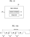
- FIG. 13 is a diagram illustrating an embodiment of the timing controller shown in FIG. 1 .
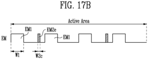
- FIGS. 14A to 16B are diagrams illustrating an embodiment of disable emission control signals corresponding to a control of the timing controller.
- FIG. 13 only components desired for description of the disclosure will be illustrated. In FIG. 13 , components overlapping with those shown in FIG. 8 will be briefly described.
- the timing controller 120 may include a storage unit 122 and a luminance determiner 124.
- Information of the first width W1, the second width W2, and/or the third width W3, which are shown in FIGS. 7A , 7B , 14A , and 14B may be stored in the storage unit 122.
- information of second widths W2a, W2b, and W2c and/or third widths W3a and W3b, which are shown in FIGS. 15A to 17B may be stored in the storage unit 122.
- the luminance determiner 124 may determine a luminance in a frame unit, using input data Din.
- the luminance determiner 124 may calculate an onpixel ratio ("OPR") of the input data Din, and determine the luminance in the frame unit, based on the OPR.
- the OPR may be a ratio of pixels activated based on the input data Din with respect to the number of pixels PX included in the pixel unit 110.
- the luminance determiner 124 may determine the luminance in the frame unit, using a grayscale value of the input data Din.
- Various methods currently known in the art may be used as a method of determining the luminance in the luminance determiner 124.
- the luminance determiner 124 may determine a relatively high luminance (e.g., above a first luminance threshold), an intermediate luminance, and a relatively low luminance in the frame unit. In an embodiment, when the OPR is 90% (as example of first luminance threshold) or more, the luminance determiner 124 may determine a luminance in a current frame as the relatively high luminance, for example. In an embodiment, when the OPR is 10% (as an example of a second luminance threshold being less than the first luminance threshold and/or which may be separated by a luminance interval from each other) or less, the luminance determiner 124 may determine the luminance of the current frame as the relatively low luminance, for example.
- the luminance determiner 124 may determine the luminance of the current frame as the intermediate luminance, for example.
- the above-described numerical values of about 90% and about 10% are merely illustrative, and may be experimentally and variously set.
- the timing controller 120 may change positions (e.g., timings, times or the like) at which a second emission control signal EM2 and/or a third emission control signal EM3 are supplied as shown in FIGS. 14A and 14B , corresponding to the luminance in the frame unit, which is determined in the luminance determiner 124.
- the timing controller 120 may set a second disable emission control signal EM supplied in the active area Active Area to have the second width W2 and set a third disable emission control signal EM supplied in the active area Active Area to have the third width W3 as shown in FIG. 14A .
- the widths of the second disable emission control signal EM and the third disable emission control signal EM may be set relatively wide such that a luminance difference corresponding to the change in image refresh rate may be minimized.
- the timing controller 120 may set a third disable emission control signal EM supplied in the active area Active Area to have the second width W2 and set a fourth disable emission control signal EM supplied in the active area Active Area to have the third width W3 as shown in FIG. 14B .
- the widths of the third disable emission control signal EM and the fourth disable emission control signal EM may be set relatively wide such that a flicker may be minimized.
- the timing controller 120 may set a second disable emission control signal EM supplied in the active area Active Area to have the second width W2 and set a fourth disable emission control signal EM supplied in the active area Active Area to have the third width W3 as shown in FIG. 7A .
- the timing controller may change widths of second emission control signals EM2a and EM2b and third emission control signals EM3a and EM3b as shown in FIGS. 15A and 15B .
- the timing controller 120 may set a second disable emission control signal EM supplied in the active area Active Area to have a second width W2a and set a fourth disable emission control signal EM supplied in the active area Active Area to have a third width W3a as shown in FIG. 15A .
- the second width W2a may be set as a relatively wide width as compared with the second width W2 shown in FIG. 7A .
- the third width W3a may be set as a relatively wide width as compared with the third width W3 shown in FIG. 7A .
- the second width W2a and the third width W3a may be set as widths equal to or different from each other.
- the widths of a second emission control signal EM2a and a third emission control signal EM3a may be set relatively wide by considering the luminance difference corresponding to the change in image refresh rate.
- the timing controller 120 may set a second disable emission control signal EM supplied in the active area Active Area to have a second width W2b and set a fourth disable emission control signal EM supplied in the active area Active Area to have a third width W3b as shown in FIG. 15B .
- the second width W2b may be set as a narrow width as compared with the second width W2 shown in FIG. 7A .
- the third width W3b may be set as a narrow width (e.g., narrower) as compared with the third width W3 shown in FIG. 7A .
- the timing controller 120 may set a second disable emission control signal EM supplied in the active area Active Area to have the second width W2 and set a fourth disable emission control signal EM supplied in the active area Active Area to have the third width W3 as shown in FIG. 7A .
- the second width W2 may be set as a width which is narrower than the second width W2a and is wider than the second width W2b.
- the third width W3 may be set as a width which is narrower than the third width W3a and is wider than the third width W3b.
- each of the second emission control signals EM2a and EMA2b is supplied as the second emission control signal in the active area Active Area
- each of the third emission control signals EM3a and EM3b is supplied as the fourth emission control signal in the active area Active Area.
- the disclosure is not limited thereto.
- each of the second emission control signals EM2a and EM2b is supplied as the second emission control signal in the active area Active Area
- each of the third emission control signals EM3a and EM3b is supplied as the third emission control signal in the active area Active Area.
- the timing controller 120 may change positions at which second emission control signals EM2c and EM2d and third emission control signals EM3c and EM3d are supplied and widths of the second emission control signals EM2c and EM2d and the third emission control signals EM3c and EM3d as shown in FIGS. 16A and 16B , corresponding to the luminance in the frame unit, which is determined in the luminance determiner 124.
- the timing controller 120 may set a second disable emission control signal EM supplied in the active area Active Area to have the second width W2a and set a third disable emission control signal EM supplied in the active area Active Area to have the third width W3a as shown in FIG. 16A .
- the timing controller 120 may set a third disable emission control signal EM supplied in the active area Active Area to have the second width W2b and set a fourth disable emission control signal EM supplied in the active area Active Area to have the third width W3b as shown in FIG. 16B .
- the timing controller 120 may set a second disable emission control signal EM supplied in the active area Active Area to have the second width W2 and set a fourth disable emission control signal EM supplied in the active area Active Area to have the third width W3 as shown in FIG. 7A .
- FIGS. 17A and 17B are diagrams illustrating an embodiment of an emission control signal supplied during one frame period.
- the emission driver 150 may supply a disable emission control signal EM having at least two different widths during an active area Active Area of one frame under the control of the timing controller 120.
- the emission driver 150 may supply a first emission control signal EM1 having a first width W1 and a second emission control signal EM2e having a second width W2c.
- the second width W2c may be set as a narrow width as compared with the first width W1.
- the first emission control signal EM 1 may be supplied in the same cycle (or the same interval) during the active area Active Area and a blank area Blank Area of the one frame.
- the second emission control signal EM2e may be supplied between first emission control signals EM1 during the active area Active Area of the one frame.
- the second emission control signal EM2e may be supplied between a first first emission control signal EM1 and a second first emission control signal EM1 (or a period 1 Cycle) and between a third first emission control signal EM1 and a fourth first emission control signal EM1 (or a period 3 Cycle).
- the emission driver 150 may change a position at which the second emission control signal EM2e is supplied in a unit of at least one frame.
- a second emission control signal EM2e shown in FIG. 17A and a second emission control signal EM2e shown in FIG. 17B may be supplied at different positions (or different times) during the active area Active Area.
- the flicker may be additionally reduced or prevented.
- the width of an emission control signal supplied in an active area is controlled, so that a luminance difference (or flicker) in one frame and a luminance difference caused by a change in image refresh rate may be minimized.
- the width of an emission control signal supplied in an active area is controlled corresponding to a luminance of one frame, so that display quality may be improved.
Landscapes
- Engineering & Computer Science (AREA)
- Physics & Mathematics (AREA)
- Computer Hardware Design (AREA)
- General Physics & Mathematics (AREA)
- Theoretical Computer Science (AREA)
- Chemical & Material Sciences (AREA)
- Crystallography & Structural Chemistry (AREA)
- Control Of Indicators Other Than Cathode Ray Tubes (AREA)
Abstract
Description
- The disclosure generally relates to a display device and a method of driving the same.
- With the development of information technologies, the importance of a display device which is a connection medium between a user and information increases. Accordingly, display devices such as a liquid crystal display device and an organic light-emitting display device are increasingly used.
- A high-speed driving function of providing users with images changed at a high frame frequency and a low-speed driving function of providing users with images changed at a low frame frequency are desired in recent display devices. A method capable of providing images with similar luminances and minimizing flickers when a display device is driven at a high frequency and a low frequency is desired.
- Embodiments provide a display device and a method of driving the same, which may minimize a luminance difference in one frame.
- Embodiments also provide a display device and a method of driving the same, which may minimize a luminance difference when the display device is driven at a relatively high frequency and a relatively low frequency.
- In an embodiment of the disclosure, there is provided a display device including: pixels each connected to a corresponding scan line among scan lines, a corresponding data line among data lines, and a corresponding emission control line among emission control lines; and an emission driver which supplies an emission control signal to the emission control lines, where the emission control signal includes a first emission control signal having a first width and at least one second emission control signal having a second width during an active area of one frame.
- In an embodiment, the emission driver may supply the first emission control signal during a writing period in which a data signal is supplied to the pixels in the active area, and supply the second emission control signal during a period except the writing period in the active area.
- In an embodiment, the second width may be set as a relatively wide width as compared with the first width.
- In an embodiment, the emission driver may further supply a third emission control signal having a third width during the period except the writing period in the active area.
- In an embodiment, the third width may be set as a relatively wide width as compared with the first width, and the second width and the third width may be set as widths equal to or different from each other.
- In an embodiment, the second emission control signal may be supplied as a second active area emission control signal in the active area, and the third emission control signal may be supplied as a fourth active area emission control signal in the active area.
- In an embodiment, the second emission control signal may be supplied as a second active area emission control signal in the active area, and the third emission control signal may be supplied as a third active area emission control signal in the active area.
- In an embodiment, the display device may further include a timing controller which controls the emission driver. The timing controller may include a storage unit in which information of the first width, the second width, and the third width is stored.
- In an embodiment, the timing controller may further include a luminance determiner which determines a luminance in a unit of the one frame, corresponding to input data.
- In an embodiment, the timing controller may change positions at which the second emission control signal and the third emission control signal are supplied, corresponding to the luminance.
- In an embodiment, when the luminance of the one frame is determined as a relatively high luminance, the timing controller may supply the second emission control signal as a second active area emission control signal in the active area, and supply the third emission control signal as a third emission control signal in the active area.
- In an embodiment, when the luminance of the one frame is determined as a relatively low luminance, the timing controller may supply the second emission control signal as a third active area emission control signal in the active area, and supply the third emission control signal as a fourth active area emission control signal in the active area.
- In an embodiment, the timing controller may change widths of the second emission control signal and the third emission control signal, corresponding to the luminance.
- In an embodiment, the timing controller may increase the widths of the second emission control signal and the third emission control signal when the luminance of the one frame is determined as a relatively high luminance, and decrease the widths of the second emission control signal and the third emission control signal when the luminance of the one frame is determined as a relatively low luminance.
- In an embodiment, the second width may be set as a width narrower than the first width, and the emission driver may supply the first emission control signal in a predetermined cycle during an active area and a blank area of one frame.
- In an embodiment, the display device may further include a timing controller which controls the emission driver, and the timing controller may change a position at which the second emission control signal is supplied in a unit of at least one frame.
- In an embodiment of the disclosure, there is provided a method of driving a display device including a pixel of which emission time is controlled corresponding to an emission control signal, the method including: supplying an emission control signal having a first width and an emission control signal having a second width different from the first width during an active area of one frame; and supplying the emission control signal having the first width during a blank area of the one frame.
- In an embodiment, the second width may be set as a relatively wide width as compared with the first width.
- In an embodiment, a length of the second width may be changed corresponding to a luminance of the one frame.
- In an embodiment, the emission control signal having the first width may be supplied in a predetermined cycle in the active area and the blank area. The second width may be set as a width narrower than the first width, and a position at which the emission control signal having the second width is supplied may be changed in a unit of at least one frame.
- Embodiments will now be described more fully hereinafter with reference to the accompanying drawings.
-
FIG. 1 is a diagram illustrating an embodiment of a display device in accordance with the disclosure. -
FIG. 2 is a diagram illustrating an embodiment of a scan driver and an emission driver, which are shown inFIG. 1 . -
FIG. 3 is a diagram illustrating an embodiment of a pixel in accordance with the disclosure. -
FIG. 4 is a waveform diagram illustrating an embodiment of a method of driving the pixel shown inFIG. 3 during a writing period. -
FIG. 5 is a waveform diagram illustrating an embodiment of the method of driving the pixel shown inFIG. 3 during a maintenance period. -
FIG. 6 is a diagram illustrating a luminance of one frame period. -
FIGS. 7A and7B are diagram illustrating an embodiment of emission control signals supplied during an active area. -
FIG. 8 is a diagram illustrating an embodiment of a timing controller shown inFIG. 1 . -
FIG. 9 is a diagram illustrating a luminance of one frame period of display devices. -
FIG. 10 is a diagram illustrating an embodiment of an embodiment of a method of setting a width of an emission control signal in accordance with the disclosure. -
FIG. 11 is a diagram illustrating flicker characteristics of an embodiment of the disclosure and a comparative example. -
FIG. 12 is a diagram illustrating luminance difference characteristics of an embodiment of the disclosure and a comparative example. -
FIG. 13 is a diagram illustrating an embodiment of the timing controller shown inFIG. 1 . -
FIGS. 14A to 16B are diagrams illustrating an embodiment of disable emission control signals corresponding to a control of the timing controller. -
FIGS. 17A and17B are diagrams illustrating an embodiment of an emission control signal supplied during one frame period. - Hereinafter, embodiments are described in detail with reference to the accompanying drawings so that those skilled in the art may easily practice the disclosure. The disclosure may be implemented in various different forms and is not limited to the embodiments described in the specification.
- A part irrelevant to the description will be omitted to clearly describe the disclosure, and the same or similar constituent elements will be designated by the same reference numerals throughout the specification. Therefore, the same reference numerals may be used in different drawings to identify the same or similar elements.
- In addition, the size and thickness of each component illustrated in the drawings are arbitrarily shown for better understanding and ease of description, but the disclosure is not limited thereto. Thicknesses of several portions and regions are exaggerated for clear expressions.
- In description, the expression "equal" may mean "substantially equal." That is, this may mean equality to a degree to which those skilled in the art may understand the equality. Other expressions may be expressions in which "substantially' is omitted.
- Some embodiments are described in the accompanying drawings in relation to functional blocks, units, and/or modules. Those skilled in the art will understand that these blocks, units, and/or modules are physically implemented by logic circuits, individual components, microprocessors, hard wire circuits, memory elements, line connection, and other electronic circuits. This may be formed by semiconductor-based manufacturing techniques or other manufacturing techniques. In the case of blocks, units, and/or modules implemented by microprocessors or other similar hardware, the units, and/or modules are programmed and controlled by software, to perform various functions discussed in the disclosure, and may be selectively driven by firmware and/or software. In addition, each block, each unit, and/or each module may be implemented by dedicated hardware or by a combination dedicated hardware to perform some functions of the block, the unit, and/or the module and a processor (e.g., one or more programmed microprocessors and associated circuitry) to perform other functions of the block, the unit, and/or the module. In some embodiments, the blocks, the units, and/or the modules may be physically separated into two or more individual blocks, two or more individual units, and/or two or more individual modules without departing from the scope of the disclosure. Also, in some embodiments, the blocks, the units, and/or the modules may be physically separated into more complex blocks, more complex units, and/or more complex modules without departing from the scope of the disclosure.
- The term "connection" between two components may include both electrical connection and physical connection, but the disclosure is not necessarily limited thereto. For example, the term "connection" used based on circuit diagrams may mean electrical connection, and the term "connection" used based on cross-sectional and plan views may mean physical connection.
- It will be understood that, although the terms "first," "second," etc. may be used herein to describe various elements, these elements should not be limited by these terms. These terms are only used to distinguish one element from another element. Thus, a "first" element discussed below could also be termed a "second" element without departing from the teachings of the disclosure.
- In the drawing figures, dimensions may be exaggerated for clarity of illustration. It will be understood that when an element is referred to as being "between" two elements, it can be the only element between the two elements, or one or more intervening elements may also be present. Like reference numerals refer to like elements throughout.
- "About" or "approximately" as used herein is inclusive of the stated value and means within an acceptable range of deviation for the particular value as determined by one of ordinary skill in the art, considering the measurement in question and the error associated with measurement of the particular quantity (i.e., the limitations of the measurement system). The term such as "about" can mean within one or more standard deviations, or within ± 30%, 20%, 10%, 5% of the stated value, for example.
- Unless otherwise defined, all terms (including technical and scientific terms) used herein have the same meaning as commonly understood by one of ordinary skill in the art to which this disclosure belongs. It will be further understood that terms, such as those defined in commonly used dictionaries, should be interpreted as having a meaning that is consistent with their meaning in the context of the relevant art and the present disclosure, and will not be interpreted in an idealized or overly formal sense unless expressly so defined herein.
- The disclosure is not limited to embodiments disclosed below, and may be implemented in various forms. Each embodiment disclosed below may be independently embodied or be combined with at least another embodiment prior to being embodied.
-
FIG. 1 is a diagram illustrating an embodiment of a display device in accordance with the disclosure.FIG. 2 is a diagram illustrating an embodiment of a scan driver and an emission driver, which are shown inFIG. 1 . - Referring to
FIG. 1 , thedisplay device 100 in the embodiment of the disclosure includes pixels PX each electrically connected to a corresponding scan line among a plurality of scan lines, a corresponding data line among a plurality of data lines, and a corresponding and a corresponding emission control line among a plurality of emission control lines. Thedisplay device 100 may include a pixel unit 110 (or panel), atiming controller 120, ascan driver 130, adata driver 140, anemission driver 150, and apower supply 160. The disclosure is not restricted to thedisplay device 100 according toFIGS. 1 and2 andother display devices 100 can be used to implement the concepts of the present disclosure. - The
display device 100 may display an image at various image refresh rates (e.g., driving frequencies or screen refresh rates) according to driving conditions. The image refresh rate means a frequency at which a data signal is written to a driving transistor of a pixel PX. In an embodiment, the image refresh rate may also be referred to as a screen scan rate or a screen refresh frequency, and represent a frequency at which a display screen is reproduced for one second, for example. - In an embodiment, an output frequency of the
data driver 140 with respect to one horizontal line (e.g., pixels PX connected to the same scan line may be sorted as one horizontal line (or pixel row)) and/or an output frequency of asecond scan driver 134 which outputs a second scan signal (or writing scan signal) may be determined corresponding to the image refresh rate. In an embodiment, an image refresh rate for driving a moving image may be a frequency of about 60 hertz (Hz) or higher (e.g., about 120 Hz, about 240 Hz, or the like), for example. - In an embodiment, the
display device 100 may display an image, corresponding to various image refresh rates of about 1 Hz to about 240 Hz, for example. However, this is merely illustrative, and thedisplay device 100 may also display an image at an image refresh rate of about 240 Hz or higher (e.g., about 480 Hz). - The
pixel unit 110 may include pixels PX connected to first scan lines SL11, SL12, ..., and SL1n, second scan lines SL21, SL22, ..., and SL2n, third scan lines SL31, SL32, ..., and SL3n, fourth scan lines SL41, SL42, ..., and SL4n, data lines DL1, DL2, ..., and DLm, emission control lines EL1, EL2, ..., and ELo, and power lines PL1, PL2, PL3, ,PL4 and PL5(n, m, and o are natural numbers of 2 or more). - In an embodiment, a pixel PXij (refer to
FIG. 3 as a suitable example but the invention is not restricted thereto and other circuits for pixels may be implemented) disposed on an ith horizontal line (or pixel row) and a jth vertical line (or pixel column) may be connected to an ith first scan line SL1i, an ith second scan line SL2i, an ith third scan line SL3i, an ith fourth scan line SL4i, a kth emission control line ELk, and a jth data line DLj (i is an integer of n or less, j is an integer of m or less, and k is an integer of o or less). Here, k is a natural number which is equal to i or is smaller than i. In an embodiment, when each of the emission control lines EL1 to ELo is connected to pixels PX disposed on one horizontal line, k may be a natural number equal to i. In an embodiment, when each of the emission control lines EL1 to ELo is connected to pixels PX disposed on at least two horizontal lines, k may be a natural number smaller than i. - The pixels PX may be selected in units of horizontal lines when an enable first scan signal is supplied to the first scan lines SL11 to SL1n, and each of the pixels PX selected by the enable first scan signal may be supplied with a data signal from a data line (any one of DL1 to DLm) connected thereto. The pixel PX supplied with the data signal may generate light with a predetermined luminance, corresponding to a voltage of the data signal.
- The
scan driver 130 may receive a scan driving signal SCS from thetiming controller 120. At least one scan start signal and clock signals, which are desired for driving of thescan driver 130, may be included in the scan driving signal SCS. Thescan driver 130 may generate the enable first scan signal, an enable second scan signal, an enable third scan signal, and an enable fourth scan signal while shifting the scan start signal, corresponding to the clock signal. - To this end, the
scan driver 130 may include afirst scan driver 132, thesecond scan driver 134, athird scan driver 136, and afourth scan driver 138 as shown inFIG. 2 . At least some of thescan drivers - The
first scan driver 132 may receive a first scan start signal FLM1, and generate the enable first scan signal while shifting the first scan start signal FLM1, corresponding to the clock signal. Thefirst scan driver 132 may sequentially supply the enable first scan signal to the first scan lines SL11 to SL1n. In an embodiment, thefirst scan driver 132 may supply the enable first scan signal during a writing period in an active area of one frame. - The
second scan driver 134 may receive a second scan start signal FLM2, and generate the enable second scan signal while shifting the second scan start signal FLM2, corresponding to the clock signal. Thesecond scan driver 134 may sequentially supply the enable second scan signal to the second scan lines SL21 to SL2n. In an embodiment, thesecond scan driver 134 may supply the enable second scan signal during the writing period in the active area of the one frame. - The
third scan driver 136 may receive a third scan start signal FLM3, and generate the enable third scan signal while shifting the third scan start signal FLM3, corresponding to the clock signal. Thethird scan driver 136 may sequentially supply the enable third scan signal to the third scan lines SL31 to SL3n. In an embodiment, thethird scan driver 136 may supply the enable third scan signal during the writing period in the active area of the one frame. - The
fourth scan driver 138 may receive a fourth scan start signal FLM4, and generate the enable fourth scan signal while shifting the fourth scan start signal FLM4, corresponding to the clock signal. Thefourth scan driver 138 may sequentially supply the enable fourth scan signal to the fourth scan lines SL41 to SL4n. In an embodiment, thefourth scan driver 138 may supply the enable fourth scan signal during the writing period in the active area of the one frame. In an embodiment, thefourth scan driver 138 may supply the enable fourth scan signal during a maintenance period included in the active area and a blank area of the one frame. - In an embodiment, the
fourth scan driver 138 may perform scanning once during the writing period of the one frame (i.e., supply at least one enable fourth scan signal), and perform scanning at least once according to the image refresh rate during the maintenance period of the one frame, for example. When the image refresh rate is decreased (i.e., when a frame length is lengthened), the blank area of the one frame is lengthened, and hence a number of maintenance periods included in the blank area may be increased. That is, when the image refresh rate is decreased, a number of times an operation of supplying the enable fourth scan signal is repeated may be increased. - Each of the enable first scan signal, the enable second scan signal, the enable third scan signal, and the enable fourth scan signal may be set to a gate-on voltage such that transistors included in the pixels PX may be turned on. In an embodiment, each of an enable first scan signal GW, an enable second scan signal GC, an enable third scan signal GI, and an enable fourth scan signal GB, which are supplied to a P-type transistor as shown in
FIG. 3 , may be set to a relatively low level voltage. - In
FIG. 2 and in view ofFIG. 1 , it is illustrated that thefirst scan driver 132, thesecond scan driver 134, thethird scan driver 136, and thefourth scan driver 138 are respectively connected to a first scan line SL1, a second scan line SL2, a third scan line SL3, and a fourth scan line SL4. However, the disclosure is not limited thereto. In an embodiment, at least two scan lines (at least two of SL1, SL2, SL3, and SL4) among the first scan line SL1, the second scan line SL2, the third scan line SL3, and the fourth scan line SL4 may be driven by one scan driver. - The
data driver 140 may receive output data Dout and a data driving signal DCS from thetiming controller 120. The data driving signal DCS may include a sampling signal and/or timing signals, desired for driving of thedata driver 140. Thedata driver 140 may generate a data signal, based on the data driving signal DCS and the output data Dout. In an embodiment, thedata driver 140 may generate an analog data signal, based on a grayscale of the output data Dout. Thedata driver 140 may supply the data signal in one horizontal period unit. - The
emission driver 150 may receive an emission driving signal ECS from thetiming controller 120. An emission start signal and clock signals, which are desired for driving theemission driver 150, may be included in the emission driving signal ECS. Theemission driver 150 may generate a disable emission control signal (or relatively high level emission control signal) EM (refer toFIG. 3 ) while shifting the emission start signal, corresponding to the clock signal. - As shown in
FIG. 2 , theemission driver 150 may receive an emission start signal EFLM, and generate the disable emission control signal EM while shifting the emission start signal EFLM, corresponding to the clock signal. Theemission driver 150 may sequentially supply the disable emission control signal EM to the emission control lines EL1 to ELo. The disable emission control signal EM may be set to a gate-off voltage such that the transistors included in the pixels PX may be turned off. In an embodiment, the disable emission control signal EM supplied to the P-type transistor as shown inFIG. 3 may be set to a relatively high level voltage. - In an embodiment, the
emission driver 150 may supply the disable emission control signal EM during the writing period and the maintenance period of the one frame. In an embodiment, theemission driver 150 may perform scanning once during the writing period of the one frame, and perform scanning at least once according to the image refresh rate during the maintenance period of the one frame, for example. When the image refresh rate is decreased (i.e., when the frame length is lengthened), the blank area of the one frame is lengthened, and hence the number of maintenance periods included in the blank area may be increased. That is, when the image refresh rate is decreased, a number of times an operation of supplying the disable emission control signal EM is repeated may be increased. - The
timing controller 120 may receive input data Din and a control signal CS from a host system through an interface. In an embodiment, thetiming controller 120 may receive the input data Din and the control signal CS from at least one of a graphics processing unit ("GPU"), a central processing unit ("CPU"), and an application processor ("AP"), which are included in the host system. Various signals including a clock signal may be included in the control signal CS. - The
timing controller 120 may generate the scan driving signal SCS, the data driving signal DCS, and the emission driving signal ECS, based on the control signal CS. The scan driving signal SCS, the data driving signal DCS, and the emission driving signal ECS may be supplied to thescan driver 130, thedata driver 140, and theemission driver 150, respectively. - The
timing controller 120 may realign the input data Din to be suitable for specifications of thedisplay device 100. Also, thetiming controller 120 may generate the output data Dout by correcting the input data Din, and supply the output data Dout to thedata driver 140. In an embodiment, thetiming controller 120 may correct the input data Din, corresponding to an optical measurement result measured in a processing process. - The
power supply 160 may generate various power sources desired for driving of thedisplay device 100. In an embodiment, thepower supply 160 may generate a first driving power source VDD, a second driving power source VSS, a first initialization power source Vint1, a second initialization power source Vint2, and a bias power source Vbias. - The first driving power source VDD may be a power source which supplies a driving current to the pixels PX. The second driving power source VSS may be a power source which is supplied with the driving current from the pixels PX. The first driving power source VDD may be set to a voltage higher than a voltage of the second driving power source VSS during a period in which the pixels PX is set to be in an emission state.
- The first initialization power source Vint1 may be a power source for initializing a gate electrode a driving transistor included in each of the pixels PX. The first initialization power source Vint1 may be set to a voltage lower than a voltage of the data signal. The second initialization power source Vint2 may be a power source for initializing a first electrode (or anode electrode) of a light-emitting element LD (refer to
FIG. 3 ) included in each of the pixels PX. The second initialization power source Vint2 may be set to a voltage at which the light-emitting element LD is turned off. The bias power source Vbias may be a power source for applying an on-bias voltage to the driving transistor included in each of the pixels PX. - The first driving power source VDD generated by the
power supply 160 may be supplied to a first power line PL1, the second driving power source VSS generated by thepower supply 160 may be supplied to a second power line PL2, the first initialization power source Vint1 generated by thepower supply 160 may be supplied to a third power line PL3, the second initialization power source Vint2 generated by thepower supply 160 may be supplied to a fourth power line PL4, and the bias power source Vbias generated by thepower supply 160 may be supplied to a fifth power line PL5. The first power line PL1, the second power line PL2, the third power line PL3, the fourth power line PL4, and the fifth power line PL5 may be commonly connected to the pixels PX, but the disclosure is not limited thereto. - In an embodiment, the first power line PL1 may be configured with a plurality of power lines, and the plurality of power lines may be connected to different pixels PX. In an embodiment, the second power line PL2 may be configured with a plurality of power lines, and the plurality of power lines may be connected to different pixels PX. In an embodiment, the third power line PL3 may be configured with a plurality of power lines, and the plurality of power lines may be connected to different pixels PX. In an embodiment, the fourth power line PL4 may be configured with a plurality of power lines, and the plurality of power lines may be connected to different pixels PX. In an embodiment, the fifth power line PL5 may be configured with a plurality of power lines, and the plurality of power lines may be connected to different pixels PX. That is, in an embodiment of the disclosure, the pixels PX may be connected to any one of the plurality of power lines of the first power line PL1, any one of the plurality of power lines of the second power line PL2, any one of the plurality of power lines of the third power line PL3, any one of the plurality of power lines of the fourth power line PL4, and any one of the plurality of power lines of the fifth power line PL5.
- In an embodiment of the disclosure, the
display device 100 may include a flat display device, a curved display device in which a portion of thepixel unit 110 is curved, a flexible display device in which a portion of thepixel unit 110 is folded or bent, and a stretchable display device in which a portion of thepixel unit 110 is expanded/contracted. - In an embodiment of the disclosure, the display device is a device which displays moving images or still images, and may include portable electronic devices such as a mobile phone, a smartphone, a tablet personal computer ("PC"), a smart watch, a watch phone, a portable multimedia player ("PMP"), a navigation system, and an ultra mobile computer ("UMPC"). In an embodiment of the disclosure, the
display device 100 may include electronic devices such as a television, a notebook computer, a monitor, an advertisement board, and Internet of things ("IoT"). -
FIG. 3 is a diagram illustrating an embodiment of a pixel in accordance with the disclosure. InFIG. 3 , a pixel PXij disposed on an ith horizontal line and a jth vertical line will be illustrated. The disclosure is not restricted to the circuit of the pixel according toFIG. 3 and other circuitry may be used to implement the concepts of the present disclosure. - Referring to
FIG. 3 , the pixel PXij in the embodiment of the disclosure may be connected to corresponding signal lines SL1i, SL2i, SL3i, SL4i, ELk, and DLj. In an embodiment, the pixel PXij may be connected to an ith first scan line SL1i, an ith second scan line SL2i, an ith third scan line SL3i, an ith fourth scan line SL4i, a kth emission control line ELk, and a jth data line DLj, for example. In an embodiment, the pixel PXij may be further connected to the first power line PL1, the second power line PL2, the third power line PL3, the fourth power line PL4, and the fifth power line PL5. - The pixel PXij in the embodiment of the disclosure may include a light-emitting element LD and a pixel circuit for controlling an amount of current supplied to the light-emitting element LD.
- The light-emitting element LD may be connected between the first power line PL1 and the second power line PL2. In an embodiment, a first electrode (or anode electrode) of the light-emitting element LD may be electrically connected to the first power line PL1 via a seventh transistor M7, a third node N3, a first transistor M1, a second node N2, and a sixth transistor M6, and a second electrode (or cathode electrode) of the light-emitting element LD may be electrically connected to the second power line PL2. The light-emitting element LD may generate light with a predetermined luminance, corresponding to an amount of current supplied from the first power line PL1 to the second power line PL2 via the pixel circuit.
- The light-emitting element LD may be selected as an organic light-emitting diode ("OLED"). Also, the light-emitting element LD may be selected as an inorganic light-emitting diode ("LED") such as a micro LED or a quantum dot LED. Also, the light-emitting element LD may be an element configured with a combination of an organic material and an inorganic material. In
FIG. 3 , it is illustrated that the pixel PXij includes a single light-emitting element LD. However, in another embodiment, the pixel PXij may include a plurality of light-emitting elements LD, and the plurality of light-emitting elements LD may be connected in series, parallel or series/parallel to each other. - The pixel circuit may include the first transistor M1, a second transistor M2, a third transistor M3, a fourth transistor M4, a fifth transistor M5, the sixth transistor M6, the seventh transistor M7, an eighth transistor M8, and a storage capacitor Cst.
- A first electrode of the first transistor M1 (or driving transistor) may be connected to the second node N2, and a second electrode of the first transistor M1 may be connected to the third node N3. In addition, a gate electrode of the first transistor M1 may be connected to a first node N1. The first transistor M1 may control an amount of current supplied from the first driving power source VDD to the second driving power source VSS via the light-emitting element LD, corresponding to a voltage of the first node N1.
- The second transistor M2 may be connected between the j-th data line DLj and the second node N2. In addition, a gate electrode of the second transistor M2 may be electrically connected to the first scan line SL1i. The second transistor M2 may be turned on when an enable first scan signal GW is supplied to the second scan line SL2i, to electrically connect the j-th data line DLj and the second node N2 to each other.
- The third transistor M3 may be connected between the first node N1 and the third node N3. In addition, a gate electrode of the third transistor M3 may be electrically connected to the second scan line SL2i. The third transistor M3 may be turned on when an enable second scan signal GC is supplied to the second scan line SL2i, to electrically connect the first node N1 and the third node N3 to each other. That is, when the third transistor M3 is turned on, the first transistor M1 may be connected in a diode form.
- A first electrode of the fourth transistor M4 may be connected to the first node N1, and a second electrode of the fourth transistor M4 may be electrically connected to the third power line PL3. In addition, a gate electrode of the fourth transistor M4 may be electrically connected to the third scan line SL3i. The fourth transistor M4 may be turned on when an enable third scan signal GI is supplied to the third scan line SL3i, to supply the voltage of the first initialization power source Vint1 to the first node N1.
- A first electrode of the fifth transistor M5 may be electrically connected to the first electrode of the light-emitting element LD, and a second electrode of the fifth transistor M5 may be electrically connected to the fourth power line PL4. In addition, a gate electrode of the fifth transistor M5 may be electrically connected to the fourth scan line SL4i. The fifth transistor M5 may be turned off when an enable fourth scan signal GB is supplied to the fourth scan line SL4i, to supply the voltage of the second initialization power source Vint2 to the first electrode of the light-emitting element LD.
- When the voltage of the second initialization power source Vint2 is supplied to the first electrode of the light-emitting element LD, a parasitic capacitor of the light-emitting element LD may be discharged. As a residual voltage charged in the parasitic capacitor of the light-emitting element LD is discharged (or removed), unintended minute emission may be prevented. Thus, the black expression ability of the pixel PXij may be improved.
- A first electrode of the sixth transistor M6 may be electrically connected to the first power line PL1, and a second electrode of the sixth transistor M6 may be connected to the second node N2. In addition, a gate electrode of the sixth transistor M6 may be electrically connected to the kth emission control line ELk. The sixth transistor M6 may be turned off when a disable emission control signal EM is supplied to the kth emission control line ELk, and be turned on when an enable emission control signal EM is supplied to the kth emission control line ELk.
- The seventh transistor M7 may be connected between the third node N3 and the first electrode of the light-emitting element LD. In addition, a gate electrode of the seventh transistor M7 may be electrically connected to the kth emission control line ELk. The seventh transistor M7 may be turned off when the disable emission control signal EM is supplied to the kth emission control line ELk, and be turned on when the enable emission control signal EM is supplied to the kth emission control line ELk.
- A first electrode of the eighth transistor M8 (or bias transistor) may be electrically connected to the fifth power line PL5, and a second electrode of the eighth transistor M8 may be connected to the second node N2. In addition, a gate electrode of the eighth transistor M8 may be electrically connected to the fourth scan line SL4i. The eighth transistor M8 may be turned on when the enable fourth scan signal GB is supplied to the fourth scan line SL4i, to electrically connect the fifth power line PL5 and the second node N2 to each other.
- The storage capacitor Cst may be connected between the first power line PL1 and the first node N1. The storage capacitor Cst may store a voltage applied to the first node N1.
- In
FIG. 3 , it is illustrated that the first to eighth transistors M1 to M8 are implemented with a P-type transistor. However, the disclosure is not limited thereto. Some transistors (e.g., M3 and M4) among the first to eighth transistors M1 to M8 may be implemented with an N-type transistor. -
FIG. 4 is a waveform diagram illustrating an embodiment of a method of driving the pixel shown inFIG. 3 during a writing period. The writing period WP may be included in an active area of a frame. - Referring to
FIGS. 3 and4 , the writing period WP may include a first period P1, a second period P2, a third period P3, and a fourth period P4. The first period P1 to the third period P3 may be set as a non-emission period, and the fourth period P4 may be set as an emission period. - During the first period P1 to the third period P3, the disable emission control signal EM may be supplied to the kth emission control line ELk. When the disable emission control signal EM is supplied to the kth emission control line ELk, the sixth transistor M6 and the seventh transistor M7 may be turned off. When the sixth transistor M6 and the seventh transistor M7 are turned off, electric connection between the first power line PL1 and the light-emitting element LD may be blocked, and accordingly, the light-emitting element LD may be set to be in a non-emission state.
- During the first period P1, the enable third scan signal GI may be supplied to the third scan line SL3i. When the enable third scan signal GI is supplied to the third scan line SL3i, the fourth transistor M4 may be turned on. When the fourth transistor M4 is turned on, the voltage of the first initialization power source Vint1 of the third power line PL3 may be supplied to the first node N1. When the voltage of the first initialization power source Vint1 is supplied to the first node N1, may be set to be in a strong on-bias state.
- During the second period P2, the enable second scan signal GC may be supplied to the second scan line SL2i, and accordingly, the third transistor M3 may be turned on. When the third transistor M3 is turned on, the first transistor M1 may be diode-connected.
- In a writing area P_W overlapping with the second period P2, the enable first scan signal GW may be supplied to the first scan line SL1i. When the enable first scan signal GW is supplied to the first scan line SL1i, the second transistor M2 may be turned on. When the second transistor M2 is turned on, a data signal from the j-th data line DLj may be supplied to the second node N2. Since the form in which the first transistor M1 is diode-connected is maintained by the turned-on third transistor M3, the first node N1 may have a voltage obtained by compensating for a threshold voltage of the first transistor M1 in the data signal.
- During the third period P3, the enable fourth scan signal GB may be supplied to the fourth scan line SL4i. When the enable fourth scan signal GB is supplied to the fourth scan line SL4i, the fifth transistor M5 and the eighth transistor M8 may be turned on. When the fifth transistor M5 is turned on, the voltage of the second initialization power source Vint2 may be supplied to the first electrode of the light-emitting element LD, and accordingly, the light-emitting element LD may be initialized. When the eighth transistor M8 is turned on, a voltage of the bias power source Vbias may be supplied to the second node N2. When the voltage of the bias power source Vbias is supplied to the second node N2, the first transistor M1 may be set to be in an on-bias state.
- In the fourth period P4, the enable emission control signal (or relatively low level emission control signal) EM may be supplied to the kth emission control line ELk, so that the sixth transistor M6 and the seventh transistor M7 are turned on. When the sixth transistor M6 and the seventh transistor M7 are turned on, a current flowing path may be formed from the first power line PL1 to the second power line PL2 via the sixth transistor M6, the first transistor M1, the seventh transistor M7, and the light-emitting element LD. A driving current corresponding to the voltage of the first node N1 may flow through the light-emitting element LD according to an operation of the first transistor M1, and the light-emitting element LD may emit light with a luminance corresponding to the driving current.
-
FIG. 5 is a waveform diagram illustrating an embodiment of the method of driving the pixel shown inFIG. 3 during a maintenance period. The waveform diagram may refer to the embodiments of thedisplay device 100 ofFIGS. 1 and2 and/or the pixel described inFIG. 3 but is not restricted thereto. The diagram may also apply toother display devices 100 and pixels PX different to the ones described as examples inFIGS. 1 ,2 and3 . The maintenance period MP is a period in which light is emitted while maintaining the voltage of a data signal supplied previously, and may be a period in which an image is displayed without changing any frame. In an embodiment, one frame may include one writing period WP in an active area thereof and a plurality of maintenance periods MP in the active area and a blank area thereof. The plurality of maintenance periods MP may be successively disposed after the writing period WP. - As compared with the writing period WP, in the maintenance period MP, a threshold voltage compensation operation and a data writing operation may be omitted, and an operation of applying a bias voltage to the first transistor M1 and an operation of initializing the light-emitting element LD may be performed. The maintenance period MP may be set to have a length similar to a length of the writing period WP. The maintenance period MP may include a first period P1a, a second period P2a, a third period P3a, and a fourth period P4a.
- Referring to
FIGS. 3 and5 , in the first period P1a to the third period P3a, the disable emission control signal EM may be supplied to the kth emission control line ELk. When the disable emission control signal EM is supplied to the kth emission control line ELk, the sixth transistor M6 and the seventh transistor M7 may be turned off, and accordingly, the light-emitting element LD may be set to be in the non-emission state. - In the first period P1a to the third period P3a, the enable first scan signal GW, the enable second scan signal GC, and the enable third scan signal GI may not be supplied (or disable scan signals GW, GC, and GI may be supplied). Accordingly, in the first period P1a to the third period P3a, the second transistor M2, the third transistor M3, and the fourth transistor M4 may be set to be in a turn-off state.
- In the third period P3a, the enable fourth scan signal GB may be supplied to the fourth scan line SL4i. When the enable fourth scan signal GB is supplied to the fourth scan line SL4i, the fifth transistor M5 and the eighth transistor M8 may be turned on.
- When the fifth transistor M5 is turned on, the voltage of the second initialization power source Vint2 may be supplied to the first electrode of the light-emitting element LD, and accordingly, the light-emitting element LD may be initialized. When the eighth transistor M8 is turned on, the voltage of the bias power source Vbias may be supplied to the second node N2. When the voltage of the bias power source Vbias is supplied to the second node N2, the first transistor M1 may be set to be in the on-bias state.
- Since the one frame includes the writing period WP and the maintenance period MP, the above-described
display device 100 in the embodiment of the disclosure may be driven at various driving frequencies (various frame frequencies). -
FIG. 6 is a diagram illustrating a luminance of one frame period according to a comparative example. The diagram may refer to the embodiments of thedisplay device 100 ofFIGS. 1 and2 and/or the pixel described inFIG. 3 but is not restricted thereto. The diagram may also apply toother display devices 100 and pixels PX different to the ones described as examples inFIGS. 1 and2 . InFIG. 6 , a luminance of pixels disposed on one horizontal line will be illustrated. InFIG. 6 , a portion indicated by Cycle may mean a period in which light the pixels emit and do not emit light in response to one emission control signal EM. InFIG. 6 , it is assumed that thedisplay device 100 is driven at about 48 Hz, and ten disable emission control signals EM are supplied during one frame period. - In an embodiment, four disable emission control signals (also referred to as first to fourth active area emission control signals, respectively) EM may be supplied in an active area Active Area. In an embodiment, the active area Active Area may include one writing period WP and three maintenance periods MP. The active area Active Area may be set to have the same length regardless of the image refresh rate, and accordingly, the number (e.g., 4) of disable emission control signals EM supplied in the active area Active Area may be set constant regardless of the image refresh rate.
- In an embodiment, six disable emission control signals EM may be supplied in a blank are Blank Area. In an embodiment, the blank are Blank Area may include six maintenance periods MP. The length of the blank area Blank Area may be differently set corresponding to the image refresh rate, and accordingly, the number of disable emission control signals EM supplied in the blank area Blank Area may be differently set corresponding to the image refresh rate.
- Referring to
FIG. 6 according to the comparative embodiment, during the one frame period, the luminance of a predetermined horizontal line may be increased during a predetermined period and then be continuously decreased. In an embodiment, the luminance of the predetermined horizontal line may be increased duringperiods 1 Cycle and 2 Cycle of the active area Active Area, and be gradually decreased after a start point of aperiod 3 Cycle. - In an embodiment, the first transistor M1 may be set to be in the strong on-bias state during the first period P1 of the writing period WP as described in
FIG. 4 . A characteristic curve of the first transistor M1 may be changed (e.g., negative shift), and the luminance of the predetermined horizontal line may be gradually increased while the characteristic curve of the first transistor M1 returns to the original place during a predetermined period (e.g., theperiods 1 Cycle and 2 Cycle) (e.g., the luminance of the predetermined horizontal lien may be gradually increased during theperiods 1 Cycle and 2 Cycle). In addition, after theperiod 3 Cycle, the luminance of the predetermined horizontal line may be gradually decreased by a leakage current of the third transistor M3 and the fourth transistor M4. - When a luminance difference is set relatively large on the predetermined horizontal line during the one frame period, this may be recognized as a flicker by a user. In an embodiment of the disclosure, the width of disable emission control signals EM supplied in the active area Active Area may be controlled so as to minimize the luminance difference on the predetermined horizontal line.
-
FIGS. 7A and7B are diagram illustrating an embodiment of emission control signals supplied during the active area. - Referring to
FIGS. 6 and 7A , the luminance of a predetermined horizontal line may be set highest theperiod 3 Cycle during the one frame period. Thus, when the luminance of theperiod 3 Cycle is decreased, the luminance difference of the predetermined horizontal line may be minimized, and accordingly, display quality may be improved. - Additionally, when the luminance is increased at an initial stage of the active area Active Area, a luminance difference from a blank area Blank Area of a previous frame may occur. Thus, when the luminance of the
period 2 Cycle is decreased, the luminance difference between the previous frame and the current frame is minimized, and accordingly, the display quality may be improved. - To this end, at least two disable emission control signals EM having different widths are supplied in the active area Active Area.
- In an embodiment, a disable emission control signal EM, which may be supplied in a writing period WP of the active area Active Area, set to have a first width W1. The disable emission control signal EM having the first width W1 may be also referred to as a first emission control signal EM1. A disable emission control signal having the first width W1 may also be supplied in a maintenance period MP of the blank area Blank Area.
- In an embodiment, at least one disable emission control signal which is included in the active area Active Area, which may be supplied in the maintenance period MP after the writing period WP, has a width different from the first width W1. In an embodiment, a second disable emission control signal EM2 supplied in the active area Active Area (or supplied in a first maintenance period MP) is set to have a second width W2. The disable emission control signal EM having the second width W2 may be also referred to as a second emission control signal EM2. In an embodiment, a fourth disable emission control signal EM supplied in the active area Active Area may be set to have a third width W3. The disable emission control signal EM having the third width W3 may be also referred to as a third emission control signal EM3.
- Each of the second width W2 and the third width W3 may be set as a relatively wide (or long) width, e.g. wider width, as compared with the first width W1. Also, the second width W2 and the third width W3 may be equal to or different from each other. In
FIG. 7A , a portion hatched by black in the disable emission control signal EM may mean a widened width (or period) as compared with the disable emission control signal EM having the first width W1. - In an embodiment, when the second disable emission control signal EM supplied in the active area Active Area is set to have the second width W2 according to the above width relations, an initial luminance of the active area Active Area is decreased, and accordingly, the luminance difference from the blank area Blank Area of the previous frame may be minimized.
- In an embodiment, when the fourth disable emission control signal EM supplied in the active area Active Area is set to have the third width W3 according to the above width relations, the luminance of the
period 3 Cycle is decreased, and accordingly, a luminance difference in the one frame may be minimized. - In
FIG. 7A , it has been described that the width of the second disable emission control signal EM and the fourth disable emission control signal EM, which are supplied in the active area Active Area, are widened. However, the disclosure is not limited thereto. - In an embodiment, the widths of the second disable emission control signal EM and a third disable emission control signal EM, which are supplied in the active area Active Area, may be set relatively wide as shown in
FIG. 7B . When the width of the third disable emission control signal EM is set as the third width W3, the luminance of theperiod 2 Cycle and/or theperiod 3 Cycle is decreased, and accordingly, the luminance difference in the one frame may be minimized. -
FIG. 8 is a diagram illustrating an embodiment of the timing controller shown inFIG. 1 . InFIG. 8 , only components desired for description of the disclosure will be illustrated. - Referring to
FIG. 8 , thetiming controller 120 may include a storage unit (e.g., memory) 122. Information of the first width W1, the second width W2, and/or the third width W3, which are shown inFIGS. 6 to 7B , may be stored in thestorage unit 122. The first width W1, the second width W2, and/or the third width W3, which are stored in thestorage unit 122, may correspond to the width (length, time) of the disable emission control signal. - In an embodiment, when the disable emission control signal EM is supplied as shown in
FIG. 7A , thetiming controller 120 may supply an emission start signal EFLM having the first width W1 during the writing period WP (or corresponding to the first emission control signal of the frame). Then, theemission driver 150 may supply a disable emission control signal EM having the first width W1 to the emission control lines EL1 to ELo. - The
timing controller 120 may supply an emission start signal EFLM having the second width W2, corresponding to the second disable emission control signal EM. Then, theemission driver 150 may supply a disable emission control signal EM having the second width W2 to the emission control lines EL1 to ELo. - The
timing controller 120 may supply an emission start signal EFLM having the third width W3, corresponding to the fourth disable emission control signal EM. Then, theemission driver 150 may supply a disable emission control signal EM having the third width W3 to the emission control lines EL1 to ELo. - The
timing controller 120 may supply the emission start signal EFLM, corresponding to the third disable emission control signal EM and the other disable emission control signals EM supplied in the blank area Blank Area. Then, theemission driver 150 may supply the disable emission control signal EM having the first width W1 to the emission control lines EL1 to ELo. The luminance difference in the one frame may be minimized by the setting the widths, for example, as shown in the embodiments and as described above with respect toFIGS. 7A and7B . -
FIG. 9 is a diagram illustrating a luminance of one frame period of display devices. InFIG. 9 , different display devices are driven at about 48 Hz, and ten disable emission control signals EM are supplied during one frame period. - Referring to
FIG. 9 , although the same data signal is supplied to the display devices, the display devices may have different luminances during the one frame period. When the display devices have different luminances, the second width W2 and/or the third width W3, which are shown inFIGS. 7A and7B , may be set to be different with respect to the display devices. - In an embodiment, the second width W2 and the third width W3 are set to be the same for each display device, a characteristic of the display device cannot be reflected. Therefore, in an embodiment of the disclosure, the second width W2 and the third width W3 may be set by reflecting the characteristic of the display device.
-
FIG. 10 is a diagram illustrating an embodiment of an embodiment of a method of setting a width of an emission control signal in accordance with the disclosure. The setting of the width of the emission control signal, which is shown inFIG. 10 , may be set for eachdisplay device 100 through multi-time programming ("MTP"). The width of the emission control signal may be set in a processing process. - Referring to
FIG. 10 , first, a width of a standard disable emission control signal EM may be loaded (S1000). In an embodiment, the width of the standard disable emission control signal EM may be set as a first width W1. In the operation S1000, the width of the standard disable emission control signal EM may be loaded by thetiming controller 120. The width of the standard disable emission control signal EM may be pre-stored in thestorage unit 122. In the operation S1000, the width of the standard disable emission control signal EM may be disposed by a separate processing device electrically connected to thetiming controller 120 in the processing process. - After the width of the standard disable emission control signal EM is loaded in the operation S1000, a width of at least one disable emission control signal among a second emission control signal EM to a fourth disable emission control signal EM, which are supplied in an active area Active Area may be changed (S1002).
- In an embodiment, in the operation S1002, the width of each of the second disable emission control signal EM (or EM2) and the fourth disable emission control signal EM (or EM3) may be changed as shown in
FIG. 7A . In an embodiment, in the operation S1002, the width of each of the second disable emission control signal EM (or EM2) and the third disable emission control signal EM (or EM3) may be changed as shown inFIG. 7B . - After the width of the disable emission control signal EM is changed in the operation S1002, it may be determined whether each of a luminance and a flicker is a threshold value or less while measuring the pixel unit 110 (S1004). In the operation S1004, the luminance may mean a luminance difference between frames, which corresponds to a change in image refresh rate. In the operation S1004, the flicker may mean a luminance difference in one frame.
- When each of the luminance and the flicker is set to the threshold value or less in the operation S1004, the width of a corresponding disable emission control signal EM may be stored in the storage unit 122 (S1006). When each of the luminance and the flicker exceeds the threshold value in the operation S1004, the operations S1000 to S1004 may be repeated.
-
FIG. 11 is a diagram illustrating flicker characteristics of an embodiment of the disclosure and a comparative example. InFIG. 11 , a flicker may mean a luminance difference corresponding to a lapse of time in one frame. InFIG. 11 , a flicker characteristic obtained by inspecting ten display devices is illustrated. InFIG. 11 , a value (or threshold value) satisfying the flicker characteristic may be -60 decibels (dB) or less. InFIG. 11 , "EMBODIMENT" may mean a case where the width of each of the second disable emission control signal EM and the fourth disable emission control signal EM, which are supplied in the active area Active Area, is set to be different as shown, for example, inFIG. 7A and7B with respect to the display devices. InFIG. 11 , "COMPARATIVE EXAMPLE" may mean a case where widths of disable emission control signals EM supplied in the active area Active Area are all set to be the same as shown, for example, inFIG. 6 . - Referring to
FIG. 11 , in the case of the disclosure, the flicker characteristic of the display devices may be set to the threshold value or less. That is, in the display devices in the embodiment of the disclosure, a luminance difference in one frame period may be minimized, and accordingly, display quality may be improved. - A flicker characteristic of some of the display devices of the comparative example may exceed the threshold value. When the flicker characteristic exceeds the threshold value, a luminance difference in one frame period may be recognized by a user. When the flicker characteristic exceeds the threshold value, the display devices may be determined as defective products, and therefore, manufacturing cost may be increased.
-
FIG. 12 is a diagram illustrating luminance difference characteristics of an embodiment of the disclosure and a comparative example. InFIG. 12 , a luminance difference may mean a luminance difference between frames, which corresponds to a change in image refresh. InFIG. 12 , a luminance difference characteristic obtained by inspecting ten display devices is illustrated. InFIG. 12 , a value (or threshold value) satisfying the luminance difference characteristic may be about 0.030 nit per hertz (nit/Hz) or less. InFIG. 12 , "EMBODIMENT" may mean a case where the width of each of the second disable emission control signal EM and the fourth disable emission control signal EM, which are supplied in the active area Active Area, is set to be different with respect to the display devices. InFIG. 12 , "COMPARATIVE EXAMPLE" may mean a case where widths of disable emission control signals EM supplied in the active area Active Area are all set to be the same. - Referring to
FIG. 12 , in the case of the disclosure, the luminance difference characteristic of the display devices may be set to the threshold value or less. That is, the display devices in the embodiment of the disclosure may generate similar luminances in each frame regardless of the change in image refresh rate, and accordingly, display quality may be improved. - A luminance difference characteristic of some of the display devices of the comparative example may exceed the threshold value. When the luminance difference characteristic exceeds the threshold value, a luminance difference corresponding to the change in image refresh rate may be recognized by a user. When the luminance difference characteristic exceeds the threshold value, the display devices may be determined as defective products, and therefore, manufacturing cost may be increased.
-
FIG. 13 is a diagram illustrating an embodiment of the timing controller shown inFIG. 1 .FIGS. 14A to 16B are diagrams illustrating an embodiment of disable emission control signals corresponding to a control of the timing controller. - In
FIG. 13 , only components desired for description of the disclosure will be illustrated. InFIG. 13 , components overlapping with those shown inFIG. 8 will be briefly described. - Referring to
FIG. 13 , thetiming controller 120 may include astorage unit 122 and aluminance determiner 124. - Information of the first width W1, the second width W2, and/or the third width W3, which are shown in
FIGS. 7A ,7B ,14A , and14B , may be stored in thestorage unit 122. In addition, information of second widths W2a, W2b, and W2c and/or third widths W3a and W3b, which are shown inFIGS. 15A to 17B , may be stored in thestorage unit 122. - The
luminance determiner 124 may determine a luminance in a frame unit, using input data Din. In an embodiment, theluminance determiner 124 may calculate an onpixel ratio ("OPR") of the input data Din, and determine the luminance in the frame unit, based on the OPR. The OPR may be a ratio of pixels activated based on the input data Din with respect to the number of pixels PX included in thepixel unit 110. In an embodiment, theluminance determiner 124 may determine the luminance in the frame unit, using a grayscale value of the input data Din. Various methods currently known in the art may be used as a method of determining the luminance in theluminance determiner 124. - In an embodiment, the
luminance determiner 124 may determine a relatively high luminance (e.g., above a first luminance threshold), an intermediate luminance, and a relatively low luminance in the frame unit. In an embodiment, when the OPR is 90% (as example of first luminance threshold) or more, theluminance determiner 124 may determine a luminance in a current frame as the relatively high luminance, for example. In an embodiment, when the OPR is 10% (as an example of a second luminance threshold being less than the first luminance threshold and/or which may be separated by a luminance interval from each other) or less, theluminance determiner 124 may determine the luminance of the current frame as the relatively low luminance, for example. In an embodiment, when the OPR exceeds about 10% and is set to less than about 90%, i.e., luminance interval between first and second luminance threshold, theluminance determiner 124 may determine the luminance of the current frame as the intermediate luminance, for example. However, the above-described numerical values of about 90% and about 10% are merely illustrative, and may be experimentally and variously set. - The
timing controller 120 may change positions (e.g., timings, times or the like) at which a second emission control signal EM2 and/or a third emission control signal EM3 are supplied as shown inFIGS. 14A and14B , corresponding to the luminance in the frame unit, which is determined in theluminance determiner 124. - In an embodiment, when the luminance of the frame is determined as the relatively high luminance (e.g., above the first luminance threshold) in the
luminance determiner 124, thetiming controller 120 may set a second disable emission control signal EM supplied in the active area Active Area to have the second width W2 and set a third disable emission control signal EM supplied in the active area Active Area to have the third width W3 as shown inFIG. 14A . When the luminance of the frame is determined as the relatively high luminance (e.g., above the first luminance threshold), the widths of the second disable emission control signal EM and the third disable emission control signal EM may be set relatively wide such that a luminance difference corresponding to the change in image refresh rate may be minimized. - In an embodiment, when the luminance of the frame is determined as the relatively low luminance (e.g., below the second luminance threshold) in the
luminance determiner 124, thetiming controller 120 may set a third disable emission control signal EM supplied in the active area Active Area to have the second width W2 and set a fourth disable emission control signal EM supplied in the active area Active Area to have the third width W3 as shown inFIG. 14B . When the luminance of the frame is determined as the relatively low luminance (e.g., below the second luminance threshold), the widths of the third disable emission control signal EM and the fourth disable emission control signal EM may be set relatively wide such that a flicker may be minimized. - In an embodiment, when the luminance of the frame is determined as the intermediate luminance (e.g., a luminance interval or range between the first and second luminance threshold) in the
luminance determiner 124, thetiming controller 120 may set a second disable emission control signal EM supplied in the active area Active Area to have the second width W2 and set a fourth disable emission control signal EM supplied in the active area Active Area to have the third width W3 as shown inFIG. 7A . - In an embodiment, when the luminance of the frame is determined as the relatively high luminance (e.g., above the first luminance threshold) in the
luminance determiner 124, the timing controller may change widths of second emission control signals EM2a and EM2b and third emission control signals EM3a and EM3b as shown inFIGS. 15A and 15B . - In an embodiment, when the luminance of the frame is determined as the relatively high luminance (e.g., above first luminance threshold) in the
luminance determiner 124, thetiming controller 120 may set a second disable emission control signal EM supplied in the active area Active Area to have a second width W2a and set a fourth disable emission control signal EM supplied in the active area Active Area to have a third width W3a as shown inFIG. 15A . The second width W2a may be set as a relatively wide width as compared with the second width W2 shown inFIG. 7A . The third width W3a may be set as a relatively wide width as compared with the third width W3 shown inFIG. 7A . The second width W2a and the third width W3a may be set as widths equal to or different from each other. When the luminance of the frame is determined as the relatively high luminance (e.g., above first luminance threshold), the widths of a second emission control signal EM2a and a third emission control signal EM3a may be set relatively wide by considering the luminance difference corresponding to the change in image refresh rate. - In an embodiment, when the luminance of the frame is determined as the relatively low luminance (e.g., below the second luminance threshold) in the
luminance determiner 124, thetiming controller 120 may set a second disable emission control signal EM supplied in the active area Active Area to have a second width W2b and set a fourth disable emission control signal EM supplied in the active area Active Area to have a third width W3b as shown inFIG. 15B . The second width W2b may be set as a narrow width as compared with the second width W2 shown inFIG. 7A . The third width W3b may be set as a narrow width (e.g., narrower) as compared with the third width W3 shown inFIG. 7A . The second width W2b and the third width W3b may be set as widths equal to or different from each other. Also, each of the second width W2b and the third width W3b may be set as a width wider than the first width W1. When the luminance of the frame is determined as the relatively low luminance, the widths of a second emission control signal EM2b and a third emission control signal EM3b may be set narrow by considering the flicker. - In an embodiment, when the luminance of the frame is determined as the intermediate luminance (e.g., luminance interval between first and second luminance threshold) in the
luminance determiner 124, thetiming controller 120 may set a second disable emission control signal EM supplied in the active area Active Area to have the second width W2 and set a fourth disable emission control signal EM supplied in the active area Active Area to have the third width W3 as shown inFIG. 7A . The second width W2 may be set as a width which is narrower than the second width W2a and is wider than the second width W2b. The third width W3 may be set as a width which is narrower than the third width W3a and is wider than the third width W3b. - In
FIGS. 15A and 15B , it is illustrated that each of the second emission control signals EM2a and EMA2b is supplied as the second emission control signal in the active area Active Area, and each of the third emission control signals EM3a and EM3b is supplied as the fourth emission control signal in the active area Active Area. However, the disclosure is not limited thereto. In an embodiment, as shown inFIG. 15B , each of the second emission control signals EM2a and EM2b is supplied as the second emission control signal in the active area Active Area, and each of the third emission control signals EM3a and EM3b is supplied as the third emission control signal in the active area Active Area. - The
timing controller 120 may change positions at which second emission control signals EM2c and EM2d and third emission control signals EM3c and EM3d are supplied and widths of the second emission control signals EM2c and EM2d and the third emission control signals EM3c and EM3d as shown inFIGS. 16A and 16B , corresponding to the luminance in the frame unit, which is determined in theluminance determiner 124. - In an embodiment, when the luminance of the frame is determined as the relatively high luminance (e.g., above the first luminance threshold) in the
luminance determiner 124, thetiming controller 120 may set a second disable emission control signal EM supplied in the active area Active Area to have the second width W2a and set a third disable emission control signal EM supplied in the active area Active Area to have the third width W3a as shown inFIG. 16A . - In an embodiment, when the luminance of the frame is determined as the relatively low luminance (e.g., below second luminance threshold) in the
luminance determiner 124, thetiming controller 120 may set a third disable emission control signal EM supplied in the active area Active Area to have the second width W2b and set a fourth disable emission control signal EM supplied in the active area Active Area to have the third width W3b as shown inFIG. 16B . - In an embodiment, when the luminance of the frame is determined as the intermediate luminance (e.g. between first and second luminance threshold) in the
luminance determiner 124, thetiming controller 120 may set a second disable emission control signal EM supplied in the active area Active Area to have the second width W2 and set a fourth disable emission control signal EM supplied in the active area Active Area to have the third width W3 as shown inFIG. 7A . -
FIGS. 17A and17B are diagrams illustrating an embodiment of an emission control signal supplied during one frame period. - Referring to
FIGS. 17A and17B , theemission driver 150 may supply a disable emission control signal EM having at least two different widths during an active area Active Area of one frame under the control of thetiming controller 120. - In an embodiment, the
emission driver 150 may supply a first emission control signal EM1 having a first width W1 and a second emission control signal EM2e having a second width W2c. The second width W2c may be set as a narrow width as compared with the first width W1. - The first emission
control signal EM 1 may be supplied in the same cycle (or the same interval) during the active area Active Area and a blank area Blank Area of the one frame. The second emission control signal EM2e may be supplied between first emission control signals EM1 during the active area Active Area of the one frame. In an embodiment, the second emission control signal EM2e may be supplied between a first first emission control signal EM1 and a second first emission control signal EM1 (or aperiod 1 Cycle) and between a third first emission control signal EM1 and a fourth first emission control signal EM1 (or aperiod 3 Cycle). - When the second emission control signal EM2e is supplied in the
period 1 Cycle, an initial luminance of the active area Active Area is decreased, and accordingly, a luminance difference from a blank area Blank Area of a previous frame may be minimized. When the second emission control signal EM2e is supplied in theperiod 3 Cycle, a luminance difference in the one frame may be minimized. - Additionally, in an embodiment of the disclosure, the
emission driver 150 may change a position at which the second emission control signal EM2e is supplied in a unit of at least one frame. In an embodiment, a second emission control signal EM2e shown inFIG. 17A and a second emission control signal EM2e shown inFIG. 17B may be supplied at different positions (or different times) during the active area Active Area. When the position at which the second emission control signal EM2e is supplied in the unit of at least one frame is changed, the flicker may be additionally reduced or prevented. - In the display device and the method of driving the same in accordance with the disclosure, the width of an emission control signal supplied in an active area is controlled, so that a luminance difference (or flicker) in one frame and a luminance difference caused by a change in image refresh rate may be minimized.
- Also, in the display device and the method of driving the same in accordance with the disclosure, the width of an emission control signal supplied in an active area is controlled corresponding to a luminance of one frame, so that display quality may be improved.
- Embodiments have been disclosed herein, and although predetermined terms are employed, they are used and are to be interpreted in a generic and descriptive sense only and not for purpose of limitation. In some instances, as would be apparent to one of ordinary skill in the art as of the filing of the application, features, characteristics, and/or elements described in connection with a particular embodiment may be used singly or in any combinations with features, characteristics, and/or elements described in connection with other embodiments unless otherwise specifically indicated.
Claims (15)
- A display device (100) comprising:pixels (PX) each electrically connected to a corresponding scan line among a plurality of scan lines (SL11, ..., SL4n), a corresponding data line among a plurality of data lines (DL1, ..., DLm), and a corresponding emission control line among a plurality of emission control lines (EL1, ..., ELo); andan emission driver (150) configured to:
supply an emission control signal (EM) to the plurality of emission control lines (EL1, ..., ELo), wherein the emission control signal (EM) includes a first emission control signal (EM1) having a first width (W1) and a second emission control signal (EM2) having a second width (W2) different from the first width (W1) during an active area (Active Area) of one frame. - The display device (100) of claim 1, wherein the emission driver (150) is configured to:supply the first emission control signal (EM1) during a writing period (WP) in which a data signal is supplied to the pixels (PX) in the active area (Active Area); andsupply the second emission control signal (EM2) during a period except the writing period (WP) in the active area (Active Area).
- The display device (100) of one of the preceding claims 1 to 2, wherein the second width (W2) is set to have a wider width compared to the first width (W1).
- The display device (100) of one of the preceding claims 2 to 3, wherein the emission driver (150) is further configured to supply a third emission control signal (EM3) having a third width (W3) during the period except the writing period (WP) in the active area (Active Area).
- The display device (100) of claim 4, wherein the third width (W3) is set to have a wider width compared to the first width (W1), and the second width (W2) and the third width (W3) are set as widths equal to or different from each other.
- The display device (100) of one of the preceding claims 4 to 5, wherein the emission driver (150) is configured to:supply the second emission control signal (EM2) as a second active area emission control signal in the active area (Active area), andsupply the third emission control signal (EM3) as a fourth active area emission control signal in the active area (Active Area).
- The display device (100) of one of the preceding claims 4 to 5, wherein the emission driver (150) is configured to:supply the second emission control signal (EM2) as a second active area emission control signal in the active area (Active area), andsupply the third emission control signal (EM3) as a third active area emission control signal in the active area (Active Area).
- The display device (100) of one of the preceding claims 1 to 7, further comprising a timing controller (120) configured to control the emission driver (150),
wherein the timing controller (120) includes a storage unit (122) in which information of the first width (W1), the second width (W2), and/or the third width (W3) is stored. - The display device (100) of claim 8, wherein the timing controller (120) further includes a luminance determiner (124) configured to determine a luminance in a unit of the one frame, corresponding to input data (Din).
- The display device (100) of claim 9, wherein the timing controller (120) is configured to change positions at which the second emission control signal (EM2) and the third emission control signal (EM3) are supplied, corresponding to the luminance.
- The display device (100) of claim 10, wherein, when the luminance of the one frame is determined to be above a first luminance threshold, the timing controller (120) is configured to:supply the second emission control signal (EM2) as a second active area emission control signal in the active area (Active Area), andsupply the third emission control signal (EM3) as a third active area emission control signal in the active area (Active Area).
- The display device (100) of one of the preceding claims 10 to 11, wherein, when the luminance of the one frame is determined to be below a second luminance threshold, the timing controller (120) is configured to:supply the second emission control signal (EM2) as a third active area emission control signal in the active area (Active Area), andsupply the third emission control signal as a fourth active area emission control signal in the active area (Active Area).
- The display device (100) of claim 9, wherein the timing controller (120) is configured to change widths of the second emission control signal (EM2a, EM2b) and the third emission control signal (EM3a, EM3b), corresponding to the luminance.
- The display device (100) of claim 13, wherein the timing controller (120) is configured to:increase the widths (W2a, W3a) of the second emission control signal (W2a) and the third emission control signal (W3a) when the luminance of the one frame is determined to be above the first luminance threshold, anddecrease the widths (W2b, W3b) of the second emission control signal (W2b) and the third emission control signal (W3b) when the luminance of the one frame is determined to be below the second luminance threshold.
- The display device (100) of one of the preceding claims 1 to 14, wherein the second width (W2c) is set to have a width narrower than the first width (W1), and the emission driver (150) is configured to supply the first emission control signal (EM1) in a predetermined cycle during an active area and a blank area of one frame; andfurther comprising a timing controller (120) configured to control the emission driver (150),wherein the timing controller (120) is configured to change a position at which the second emission control signal (EM2e) is supplied in a unit of a frame.
Applications Claiming Priority (1)
| Application Number | Priority Date | Filing Date | Title |
|---|---|---|---|
| KR1020230142363A KR20250058843A (en) | 2023-10-23 | 2023-10-23 | Display device and method of driving the same |
Publications (1)
| Publication Number | Publication Date |
|---|---|
| EP4546329A1 true EP4546329A1 (en) | 2025-04-30 |
Family
ID=93117551
Family Applications (1)
| Application Number | Title | Priority Date | Filing Date |
|---|---|---|---|
| EP24206144.8A Pending EP4546329A1 (en) | 2023-10-23 | 2024-10-11 | Display device and method of driving the same |
Country Status (4)
| Country | Link |
|---|---|
| US (1) | US12451047B2 (en) |
| EP (1) | EP4546329A1 (en) |
| KR (1) | KR20250058843A (en) |
| CN (1) | CN119889242A (en) |
Families Citing this family (1)
| Publication number | Priority date | Publication date | Assignee | Title |
|---|---|---|---|---|
| KR20260001634A (en) * | 2024-06-27 | 2026-01-06 | 삼성디스플레이 주식회사 | Pixel and driving method of the same |
Citations (3)
| Publication number | Priority date | Publication date | Assignee | Title |
|---|---|---|---|---|
| US20220028333A1 (en) * | 2020-07-23 | 2022-01-27 | Samsung Display Co., Ltd. | Pixel and a display device having the same |
| KR20220096757A (en) * | 2020-12-31 | 2022-07-07 | 엘지디스플레이 주식회사 | Organic light emitting display device |
| US20230335045A1 (en) * | 2022-09-07 | 2023-10-19 | Shanghai Tianma Microelectronics Co., Ltd. | Display panel and display device |
Family Cites Families (2)
| Publication number | Priority date | Publication date | Assignee | Title |
|---|---|---|---|---|
| KR20150006723A (en) | 2013-07-09 | 2015-01-19 | 삼성디스플레이 주식회사 | Method and apparatus for controlling optical quantities of organic light emission display device |
| KR102317876B1 (en) * | 2017-08-18 | 2021-10-28 | 삼성디스플레이 주식회사 | Organic Light Emitting Display Device and Driving Method Thereof |
-
2023
- 2023-10-23 KR KR1020230142363A patent/KR20250058843A/en active Pending
-
2024
- 2024-06-01 US US18/731,250 patent/US12451047B2/en active Active
- 2024-09-12 CN CN202411277862.9A patent/CN119889242A/en active Pending
- 2024-10-11 EP EP24206144.8A patent/EP4546329A1/en active Pending
Patent Citations (3)
| Publication number | Priority date | Publication date | Assignee | Title |
|---|---|---|---|---|
| US20220028333A1 (en) * | 2020-07-23 | 2022-01-27 | Samsung Display Co., Ltd. | Pixel and a display device having the same |
| KR20220096757A (en) * | 2020-12-31 | 2022-07-07 | 엘지디스플레이 주식회사 | Organic light emitting display device |
| US20230335045A1 (en) * | 2022-09-07 | 2023-10-19 | Shanghai Tianma Microelectronics Co., Ltd. | Display panel and display device |
Also Published As
| Publication number | Publication date |
|---|---|
| CN119889242A (en) | 2025-04-25 |
| US12451047B2 (en) | 2025-10-21 |
| KR20250058843A (en) | 2025-05-02 |
| US20250131867A1 (en) | 2025-04-24 |
Similar Documents
| Publication | Publication Date | Title |
|---|---|---|
| CN108231007B (en) | Display device and driving method thereof | |
| US11790833B2 (en) | Display device and an inspection method thereof | |
| KR102447018B1 (en) | Timing controller and display device including same | |
| US20230154405A1 (en) | Display device, driving circuit and display driving method | |
| CN114694579A (en) | Display panel and display device | |
| US12451047B2 (en) | Display device and method of driving the same | |
| CN118266020A (en) | Pixel circuit and driving method thereof, and display device | |
| US20250166564A1 (en) | Display device and method of driving the same | |
| US20250124881A1 (en) | Display device and method of driving the same | |
| KR102731160B1 (en) | Display device and Method for optimizing SOE margin of the same | |
| KR20250143893A (en) | Stage circuit and display device including the same | |
| KR20240167493A (en) | Pixel and display device including the same | |
| KR20250152135A (en) | Display device and method for setting emission control signal for the display device | |
| US12512058B2 (en) | Display device and method of driving the same | |
| EP4664442A1 (en) | Pixel,display device including the same and electronic device including display device | |
| US20260057815A1 (en) | Voltage setting method for display device, display device, and electronic device | |
| US12424149B2 (en) | Pixel and display device including the same | |
| US12579929B2 (en) | Pixel, method of driving the same, and electronic device | |
| US20250174173A1 (en) | Display device and method of driving the same | |
| US20250087156A1 (en) | Pixels and display apparatus including the same | |
| KR20250134766A (en) | Display device | |
| KR20250178195A (en) | Display device and method of driving the same | |
| KR20260073194A (en) | Voltage setting method of display devices, and display device and electronic device | |
| KR20250024620A (en) | Pixel and display device including the same | |
| CN121053913A (en) | Pixel circuits, gate driving circuits, display panels, display modules, driving methods, and electronic devices. |
Legal Events
| Date | Code | Title | Description |
|---|---|---|---|
| PUAI | Public reference made under article 153(3) epc to a published international application that has entered the european phase |
Free format text: ORIGINAL CODE: 0009012 |
|
| STAA | Information on the status of an ep patent application or granted ep patent |
Free format text: STATUS: THE APPLICATION HAS BEEN PUBLISHED |
|
| AK | Designated contracting states |
Kind code of ref document: A1 Designated state(s): AL AT BE BG CH CY CZ DE DK EE ES FI FR GB GR HR HU IE IS IT LI LT LU LV MC ME MK MT NL NO PL PT RO RS SE SI SK SM TR |
|
| STAA | Information on the status of an ep patent application or granted ep patent |
Free format text: STATUS: REQUEST FOR EXAMINATION WAS MADE |
|
| 17P | Request for examination filed |
Effective date: 20250930 |
|
| P01 | Opt-out of the competence of the unified patent court (upc) registered |
Free format text: CASE NUMBER: UPC_APP_0007520_4546329/2026 Effective date: 20260226 |