EP4546328A1 - Display device - Google Patents
Display device Download PDFInfo
- Publication number
- EP4546328A1 EP4546328A1 EP24206392.3A EP24206392A EP4546328A1 EP 4546328 A1 EP4546328 A1 EP 4546328A1 EP 24206392 A EP24206392 A EP 24206392A EP 4546328 A1 EP4546328 A1 EP 4546328A1
- Authority
- EP
- European Patent Office
- Prior art keywords
- frame period
- emission
- frmn
- sub
- cyc
- Prior art date
- Legal status (The legal status is an assumption and is not a legal conclusion. Google has not performed a legal analysis and makes no representation as to the accuracy of the status listed.)
- Pending
Links
Images




Classifications
-
- G—PHYSICS
- G09—EDUCATION; CRYPTOGRAPHY; DISPLAY; ADVERTISING; SEALS
- G09G—ARRANGEMENTS OR CIRCUITS FOR CONTROL OF INDICATING DEVICES USING STATIC MEANS TO PRESENT VARIABLE INFORMATION
- G09G3/00—Control arrangements or circuits, of interest only in connection with visual indicators other than cathode-ray tubes
- G09G3/20—Control arrangements or circuits, of interest only in connection with visual indicators other than cathode-ray tubes for presentation of an assembly of a number of characters, e.g. a page, by composing the assembly by combination of individual elements arranged in a matrix no fixed position being assigned to or needed to be assigned to the individual characters or partial characters
- G09G3/2007—Display of intermediate tones
- G09G3/2018—Display of intermediate tones by time modulation using two or more time intervals
- G09G3/2022—Display of intermediate tones by time modulation using two or more time intervals using sub-frames
- G09G3/2029—Display of intermediate tones by time modulation using two or more time intervals using sub-frames the sub-frames having non-binary weights
-
- G—PHYSICS
- G09—EDUCATION; CRYPTOGRAPHY; DISPLAY; ADVERTISING; SEALS
- G09G—ARRANGEMENTS OR CIRCUITS FOR CONTROL OF INDICATING DEVICES USING STATIC MEANS TO PRESENT VARIABLE INFORMATION
- G09G3/00—Control arrangements or circuits, of interest only in connection with visual indicators other than cathode-ray tubes
- G09G3/20—Control arrangements or circuits, of interest only in connection with visual indicators other than cathode-ray tubes for presentation of an assembly of a number of characters, e.g. a page, by composing the assembly by combination of individual elements arranged in a matrix no fixed position being assigned to or needed to be assigned to the individual characters or partial characters
-
- G—PHYSICS
- G09—EDUCATION; CRYPTOGRAPHY; DISPLAY; ADVERTISING; SEALS
- G09G—ARRANGEMENTS OR CIRCUITS FOR CONTROL OF INDICATING DEVICES USING STATIC MEANS TO PRESENT VARIABLE INFORMATION
- G09G3/00—Control arrangements or circuits, of interest only in connection with visual indicators other than cathode-ray tubes
- G09G3/20—Control arrangements or circuits, of interest only in connection with visual indicators other than cathode-ray tubes for presentation of an assembly of a number of characters, e.g. a page, by composing the assembly by combination of individual elements arranged in a matrix no fixed position being assigned to or needed to be assigned to the individual characters or partial characters
- G09G3/2007—Display of intermediate tones
- G09G3/2018—Display of intermediate tones by time modulation using two or more time intervals
- G09G3/2022—Display of intermediate tones by time modulation using two or more time intervals using sub-frames
-
- G—PHYSICS
- G09—EDUCATION; CRYPTOGRAPHY; DISPLAY; ADVERTISING; SEALS
- G09G—ARRANGEMENTS OR CIRCUITS FOR CONTROL OF INDICATING DEVICES USING STATIC MEANS TO PRESENT VARIABLE INFORMATION
- G09G3/00—Control arrangements or circuits, of interest only in connection with visual indicators other than cathode-ray tubes
- G09G3/20—Control arrangements or circuits, of interest only in connection with visual indicators other than cathode-ray tubes for presentation of an assembly of a number of characters, e.g. a page, by composing the assembly by combination of individual elements arranged in a matrix no fixed position being assigned to or needed to be assigned to the individual characters or partial characters
- G09G3/2007—Display of intermediate tones
- G09G3/2014—Display of intermediate tones by modulation of the duration of a single pulse during which the logic level remains constant
-
- G—PHYSICS
- G09—EDUCATION; CRYPTOGRAPHY; DISPLAY; ADVERTISING; SEALS
- G09G—ARRANGEMENTS OR CIRCUITS FOR CONTROL OF INDICATING DEVICES USING STATIC MEANS TO PRESENT VARIABLE INFORMATION
- G09G3/00—Control arrangements or circuits, of interest only in connection with visual indicators other than cathode-ray tubes
- G09G3/20—Control arrangements or circuits, of interest only in connection with visual indicators other than cathode-ray tubes for presentation of an assembly of a number of characters, e.g. a page, by composing the assembly by combination of individual elements arranged in a matrix no fixed position being assigned to or needed to be assigned to the individual characters or partial characters
- G09G3/22—Control arrangements or circuits, of interest only in connection with visual indicators other than cathode-ray tubes for presentation of an assembly of a number of characters, e.g. a page, by composing the assembly by combination of individual elements arranged in a matrix no fixed position being assigned to or needed to be assigned to the individual characters or partial characters using controlled light sources
- G09G3/30—Control arrangements or circuits, of interest only in connection with visual indicators other than cathode-ray tubes for presentation of an assembly of a number of characters, e.g. a page, by composing the assembly by combination of individual elements arranged in a matrix no fixed position being assigned to or needed to be assigned to the individual characters or partial characters using controlled light sources using electroluminescent panels
- G09G3/32—Control arrangements or circuits, of interest only in connection with visual indicators other than cathode-ray tubes for presentation of an assembly of a number of characters, e.g. a page, by composing the assembly by combination of individual elements arranged in a matrix no fixed position being assigned to or needed to be assigned to the individual characters or partial characters using controlled light sources using electroluminescent panels semiconductive, e.g. using light-emitting diodes [LED]
-
- G—PHYSICS
- G09—EDUCATION; CRYPTOGRAPHY; DISPLAY; ADVERTISING; SEALS
- G09G—ARRANGEMENTS OR CIRCUITS FOR CONTROL OF INDICATING DEVICES USING STATIC MEANS TO PRESENT VARIABLE INFORMATION
- G09G3/00—Control arrangements or circuits, of interest only in connection with visual indicators other than cathode-ray tubes
- G09G3/20—Control arrangements or circuits, of interest only in connection with visual indicators other than cathode-ray tubes for presentation of an assembly of a number of characters, e.g. a page, by composing the assembly by combination of individual elements arranged in a matrix no fixed position being assigned to or needed to be assigned to the individual characters or partial characters
- G09G3/22—Control arrangements or circuits, of interest only in connection with visual indicators other than cathode-ray tubes for presentation of an assembly of a number of characters, e.g. a page, by composing the assembly by combination of individual elements arranged in a matrix no fixed position being assigned to or needed to be assigned to the individual characters or partial characters using controlled light sources
- G09G3/30—Control arrangements or circuits, of interest only in connection with visual indicators other than cathode-ray tubes for presentation of an assembly of a number of characters, e.g. a page, by composing the assembly by combination of individual elements arranged in a matrix no fixed position being assigned to or needed to be assigned to the individual characters or partial characters using controlled light sources using electroluminescent panels
- G09G3/32—Control arrangements or circuits, of interest only in connection with visual indicators other than cathode-ray tubes for presentation of an assembly of a number of characters, e.g. a page, by composing the assembly by combination of individual elements arranged in a matrix no fixed position being assigned to or needed to be assigned to the individual characters or partial characters using controlled light sources using electroluminescent panels semiconductive, e.g. using light-emitting diodes [LED]
- G09G3/3208—Control arrangements or circuits, of interest only in connection with visual indicators other than cathode-ray tubes for presentation of an assembly of a number of characters, e.g. a page, by composing the assembly by combination of individual elements arranged in a matrix no fixed position being assigned to or needed to be assigned to the individual characters or partial characters using controlled light sources using electroluminescent panels semiconductive, e.g. using light-emitting diodes [LED] organic, e.g. using organic light-emitting diodes [OLED]
- G09G3/3225—Control arrangements or circuits, of interest only in connection with visual indicators other than cathode-ray tubes for presentation of an assembly of a number of characters, e.g. a page, by composing the assembly by combination of individual elements arranged in a matrix no fixed position being assigned to or needed to be assigned to the individual characters or partial characters using controlled light sources using electroluminescent panels semiconductive, e.g. using light-emitting diodes [LED] organic, e.g. using organic light-emitting diodes [OLED] using an active matrix
-
- G—PHYSICS
- G09—EDUCATION; CRYPTOGRAPHY; DISPLAY; ADVERTISING; SEALS
- G09G—ARRANGEMENTS OR CIRCUITS FOR CONTROL OF INDICATING DEVICES USING STATIC MEANS TO PRESENT VARIABLE INFORMATION
- G09G3/00—Control arrangements or circuits, of interest only in connection with visual indicators other than cathode-ray tubes
- G09G3/20—Control arrangements or circuits, of interest only in connection with visual indicators other than cathode-ray tubes for presentation of an assembly of a number of characters, e.g. a page, by composing the assembly by combination of individual elements arranged in a matrix no fixed position being assigned to or needed to be assigned to the individual characters or partial characters
- G09G3/22—Control arrangements or circuits, of interest only in connection with visual indicators other than cathode-ray tubes for presentation of an assembly of a number of characters, e.g. a page, by composing the assembly by combination of individual elements arranged in a matrix no fixed position being assigned to or needed to be assigned to the individual characters or partial characters using controlled light sources
- G09G3/30—Control arrangements or circuits, of interest only in connection with visual indicators other than cathode-ray tubes for presentation of an assembly of a number of characters, e.g. a page, by composing the assembly by combination of individual elements arranged in a matrix no fixed position being assigned to or needed to be assigned to the individual characters or partial characters using controlled light sources using electroluminescent panels
- G09G3/32—Control arrangements or circuits, of interest only in connection with visual indicators other than cathode-ray tubes for presentation of an assembly of a number of characters, e.g. a page, by composing the assembly by combination of individual elements arranged in a matrix no fixed position being assigned to or needed to be assigned to the individual characters or partial characters using controlled light sources using electroluminescent panels semiconductive, e.g. using light-emitting diodes [LED]
- G09G3/3208—Control arrangements or circuits, of interest only in connection with visual indicators other than cathode-ray tubes for presentation of an assembly of a number of characters, e.g. a page, by composing the assembly by combination of individual elements arranged in a matrix no fixed position being assigned to or needed to be assigned to the individual characters or partial characters using controlled light sources using electroluminescent panels semiconductive, e.g. using light-emitting diodes [LED] organic, e.g. using organic light-emitting diodes [OLED]
- G09G3/3225—Control arrangements or circuits, of interest only in connection with visual indicators other than cathode-ray tubes for presentation of an assembly of a number of characters, e.g. a page, by composing the assembly by combination of individual elements arranged in a matrix no fixed position being assigned to or needed to be assigned to the individual characters or partial characters using controlled light sources using electroluminescent panels semiconductive, e.g. using light-emitting diodes [LED] organic, e.g. using organic light-emitting diodes [OLED] using an active matrix
- G09G3/3233—Control arrangements or circuits, of interest only in connection with visual indicators other than cathode-ray tubes for presentation of an assembly of a number of characters, e.g. a page, by composing the assembly by combination of individual elements arranged in a matrix no fixed position being assigned to or needed to be assigned to the individual characters or partial characters using controlled light sources using electroluminescent panels semiconductive, e.g. using light-emitting diodes [LED] organic, e.g. using organic light-emitting diodes [OLED] using an active matrix with pixel circuitry controlling the current through the light-emitting element
-
- G—PHYSICS
- G09—EDUCATION; CRYPTOGRAPHY; DISPLAY; ADVERTISING; SEALS
- G09G—ARRANGEMENTS OR CIRCUITS FOR CONTROL OF INDICATING DEVICES USING STATIC MEANS TO PRESENT VARIABLE INFORMATION
- G09G5/00—Control arrangements or circuits for visual indicators common to cathode-ray tube indicators and other visual indicators
- G09G5/001—Arbitration of resources in a display system, e.g. control of access to frame buffer by video controller and/or main processor
-
- G—PHYSICS
- G09—EDUCATION; CRYPTOGRAPHY; DISPLAY; ADVERTISING; SEALS
- G09G—ARRANGEMENTS OR CIRCUITS FOR CONTROL OF INDICATING DEVICES USING STATIC MEANS TO PRESENT VARIABLE INFORMATION
- G09G2300/00—Aspects of the constitution of display devices
- G09G2300/08—Active matrix structure, i.e. with use of active elements, inclusive of non-linear two terminal elements, in the pixels together with light emitting or modulating elements
- G09G2300/0809—Several active elements per pixel in active matrix panels
- G09G2300/0819—Several active elements per pixel in active matrix panels used for counteracting undesired variations, e.g. feedback or autozeroing
-
- G—PHYSICS
- G09—EDUCATION; CRYPTOGRAPHY; DISPLAY; ADVERTISING; SEALS
- G09G—ARRANGEMENTS OR CIRCUITS FOR CONTROL OF INDICATING DEVICES USING STATIC MEANS TO PRESENT VARIABLE INFORMATION
- G09G2300/00—Aspects of the constitution of display devices
- G09G2300/08—Active matrix structure, i.e. with use of active elements, inclusive of non-linear two terminal elements, in the pixels together with light emitting or modulating elements
- G09G2300/0809—Several active elements per pixel in active matrix panels
- G09G2300/0842—Several active elements per pixel in active matrix panels forming a memory circuit, e.g. a dynamic memory with one capacitor
- G09G2300/0861—Several active elements per pixel in active matrix panels forming a memory circuit, e.g. a dynamic memory with one capacitor with additional control of the display period without amending the charge stored in a pixel memory, e.g. by means of additional select electrodes
-
- G—PHYSICS
- G09—EDUCATION; CRYPTOGRAPHY; DISPLAY; ADVERTISING; SEALS
- G09G—ARRANGEMENTS OR CIRCUITS FOR CONTROL OF INDICATING DEVICES USING STATIC MEANS TO PRESENT VARIABLE INFORMATION
- G09G2310/00—Command of the display device
- G09G2310/08—Details of timing specific for flat panels, other than clock recovery
-
- G—PHYSICS
- G09—EDUCATION; CRYPTOGRAPHY; DISPLAY; ADVERTISING; SEALS
- G09G—ARRANGEMENTS OR CIRCUITS FOR CONTROL OF INDICATING DEVICES USING STATIC MEANS TO PRESENT VARIABLE INFORMATION
- G09G2320/00—Control of display operating conditions
- G09G2320/02—Improving the quality of display appearance
- G09G2320/0233—Improving the luminance or brightness uniformity across the screen
-
- G—PHYSICS
- G09—EDUCATION; CRYPTOGRAPHY; DISPLAY; ADVERTISING; SEALS
- G09G—ARRANGEMENTS OR CIRCUITS FOR CONTROL OF INDICATING DEVICES USING STATIC MEANS TO PRESENT VARIABLE INFORMATION
- G09G2320/00—Control of display operating conditions
- G09G2320/02—Improving the quality of display appearance
- G09G2320/0247—Flicker reduction other than flicker reduction circuits used for single beam cathode-ray tubes
-
- G—PHYSICS
- G09—EDUCATION; CRYPTOGRAPHY; DISPLAY; ADVERTISING; SEALS
- G09G—ARRANGEMENTS OR CIRCUITS FOR CONTROL OF INDICATING DEVICES USING STATIC MEANS TO PRESENT VARIABLE INFORMATION
- G09G2320/00—Control of display operating conditions
- G09G2320/02—Improving the quality of display appearance
- G09G2320/0257—Reduction of after-image effects
-
- G—PHYSICS
- G09—EDUCATION; CRYPTOGRAPHY; DISPLAY; ADVERTISING; SEALS
- G09G—ARRANGEMENTS OR CIRCUITS FOR CONTROL OF INDICATING DEVICES USING STATIC MEANS TO PRESENT VARIABLE INFORMATION
- G09G2320/00—Control of display operating conditions
- G09G2320/02—Improving the quality of display appearance
- G09G2320/0271—Adjustment of the gradation levels within the range of the gradation scale, e.g. by redistribution or clipping
-
- G—PHYSICS
- G09—EDUCATION; CRYPTOGRAPHY; DISPLAY; ADVERTISING; SEALS
- G09G—ARRANGEMENTS OR CIRCUITS FOR CONTROL OF INDICATING DEVICES USING STATIC MEANS TO PRESENT VARIABLE INFORMATION
- G09G2320/00—Control of display operating conditions
- G09G2320/04—Maintaining the quality of display appearance
- G09G2320/043—Preventing or counteracting the effects of ageing
- G09G2320/045—Compensation of drifts in the characteristics of light emitting or modulating elements
-
- G—PHYSICS
- G09—EDUCATION; CRYPTOGRAPHY; DISPLAY; ADVERTISING; SEALS
- G09G—ARRANGEMENTS OR CIRCUITS FOR CONTROL OF INDICATING DEVICES USING STATIC MEANS TO PRESENT VARIABLE INFORMATION
- G09G2320/00—Control of display operating conditions
- G09G2320/06—Adjustment of display parameters
- G09G2320/0626—Adjustment of display parameters for control of overall brightness
-
- G—PHYSICS
- G09—EDUCATION; CRYPTOGRAPHY; DISPLAY; ADVERTISING; SEALS
- G09G—ARRANGEMENTS OR CIRCUITS FOR CONTROL OF INDICATING DEVICES USING STATIC MEANS TO PRESENT VARIABLE INFORMATION
- G09G2320/00—Control of display operating conditions
- G09G2320/06—Adjustment of display parameters
- G09G2320/0626—Adjustment of display parameters for control of overall brightness
- G09G2320/0653—Controlling or limiting the speed of brightness adjustment of the illumination source
-
- G—PHYSICS
- G09—EDUCATION; CRYPTOGRAPHY; DISPLAY; ADVERTISING; SEALS
- G09G—ARRANGEMENTS OR CIRCUITS FOR CONTROL OF INDICATING DEVICES USING STATIC MEANS TO PRESENT VARIABLE INFORMATION
- G09G2340/00—Aspects of display data processing
- G09G2340/04—Changes in size, position or resolution of an image
- G09G2340/0407—Resolution change, inclusive of the use of different resolutions for different screen areas
- G09G2340/0435—Change or adaptation of the frame rate of the video stream
Definitions
- Embodiments of the present disclosure relate to a display device. More particularly, embodiments of the present disclosure relate to a display device having improved image quality.
- a display device may display images having different luminances for frame periods.
- a frame period may include at least one emission period, and a pixel included in the display device may emit light in the emission period.
- An emission cycle corresponding to the number of discontinuous emission periods during one frame period may be changed between adjacent frame periods.
- flashing in which a luminance of an image displayed by the display device momentarily increases or decreases may occur.
- an image quality of the display device may deteriorate.
- Embodiments of the present disclosure provide a display device having improved image quality.
- a display device includes a display panel including a pixel and an emission line connected to the pixel, and an emission driver which provides an emission signal to the emission line.
- the emission signal defines discontinuous emission periods and non-emission periods during a frame period among a plurality of frame periods.
- the display device further includes a controller which determines an emission cycle corresponding to a number of the discontinuous emission periods during the frame period and an emission-off ratio which is a ratio of a sum of the non-emission periods to the frame period.
- the plurality of frame periods includes an n-1 th frame period, an n+1 th frame period, and an n th frame period between the n-1 th frame period and the n+1 th frame period.
- the emission cycle of the n-1 th frame period is different from the emission cycle of the n+1 th frame period, the emission-off ratio of the n-1 th frame period is equal to the emission-off ratio of the n+1 th frame period, and the n th frame period includes first to m th sub-frame periods having different emission-off ratios.
- m and n is a positive integer greater than 1.
- the emission-off ratios of the first to m th sub-frame periods may decrease from the first sub-frame period to the m th sub-frame period when the emission cycle of the n+1 th frame period is greater than the emission cycle of the n-1 th frame period.
- the emission-off ratio of the first sub-frame period may be greater than the emission-off ratio of the n-1 th frame period.
- the emission-off ratios of the first to m th sub-frame periods may increase from the first sub-frame period to the m th sub-frame period when the emission cycle of the n+1 th frame period is less than the emission cycle of the n-1 th frame period.
- the emission-off ratio of the m th sub-frame period may be greater than the emission-off ratio of the n+1 th frame period.
- the emission cycle of the n th frame period may be equal to the emission cycle of a frame period with the greater emission cycle among the n-1 th frame period and the n+1 th frame period.
- emission cycles of the first to m th sub-frames may be different.
- the emission cycles may increase from the first sub-frame period to the m th sub-frame period when the emission cycle of the n+1 th frame period is greater than the emission cycle of the n-1 th frame period.
- the emission-off ratio of the first sub-frame period may be greater than the emission-off ratio of the n-1 th frame period.
- the emission cycle of the first sub-frame period may be greater than the emission cycle of the n-1 th frame period, and the emission cycle of the m th sub-frame period may be less than the emission cycle of the n+1 th frame period.
- the emission cycles of the first to m th sub-frame periods may decrease from the first sub-frame period to the m th sub-frame period when the emission cycle of the n+1 th frame period is less than the emission cycle of the n-1 th frame period.
- the emission-off ratio of the m th sub-frame period may be greater than the emission-off ratio of the n+1 th frame period.
- the emission cycle of the first sub-frame period may be less than the emission cycle of the n-1 th frame period, and the emission cycle of the m th sub-frame period may be greater than the emission cycle of the n+1 th frame period.
- the emission cycle of the n th frame period may be between the emission cycle of the n-1 th frame period and the emission cycle of the n+1 th frame period.
- the emission cycle of one of the n-1 th frame period and the n+1 th frame period may be 1, and the emission cycle of another of the n-1 th frame period and the n+1 th frame period may be 12, 16, 24, or 32.
- luminances of the n-1 th and n+1 th frame periods may be equal.
- a display device may include a display panel including a pixel and an emission line connected to the pixel, and an emission driver which provides an emission signal to the emission line.
- the emission signal may define discontinuous emission periods and non-emission periods during a frame period among a plurality of frame periods.
- the display device may further include a controller which may determine an emission cycle corresponding to a number of the discontinuous emission periods during the frame period and an emission-off ratio which is a ratio of a sum of the non-emission periods to the frame period.
- a first frame period may have a first emission cycle
- a second frame period adjacent to the first frame period may have a second emission cycle greater than the first emission cycle
- a length of a non-emission period of the first frame period may be equal to a length of a non-emission period of the second frame period.
- the first frame period may have a first emission-off ratio which is a minimum emission-off ratio
- the second frame period may have a second emission-off ratio greater than the first emission-off ratio
- a magnitude of a data voltage of the first frame period may be less than a magnitude of a data voltage of the second frame period.
- the first emission cycle may be 1, and the second emission cycle may be 12, 16, 24, or 32.
- a buffer frame period including sub-frame periods having different emission-off ratios may be inserted between the adjacent frame periods, or lengths of non-emission periods of the adjacent frame periods may be equal. Accordingly, the flashing of the image displayed by the display device may not occur although a difference in the emission cycles between the adjacent frame periods is large.
- FIG. 1 is a block diagram showing a display device 100 according to an embodiment.
- a display device 100 may include a display panel 110, a gate driver 120 (also referred to as a gate driver circuit), a data driver 130 (also referred to as a data driver circuit), an emission driver 140 (also referred to as an emission driver circuit), and a controller 150 (also referred to as a controller circuit).
- a gate driver 120 also referred to as a gate driver circuit
- a data driver 130 also referred to as a data driver circuit
- an emission driver 140 also referred to as an emission driver circuit
- controller 150 also referred to as a controller circuit
- the display panel 110 may include a plurality of pixels PX, a plurality of gate lines GL, a plurality of data lines DL, and a plurality of emission lines EML.
- the pixels PX may include pixels that emit light of multiple colors.
- the pixels PX may include red pixels that emit red light, green pixels that emit green light, and blue pixels that emit blue light.
- the gate lines GL may be connected to the pixels PX.
- the gate lines GL may extend in a first direction D1 and be arranged in a second direction D2 crossing the first direction D1.
- the gate lines GL may provide gate signals GS to the pixels PX.
- the data lines DL may be connected to the pixels PX.
- the data lines DL may extend in the second direction D2 and be arranged in the first direction D1.
- the data lines DL may provide data voltages VDAT to the pixels PX.
- the emission lines EML may be connected to the pixels PX.
- the emission lines EML may extend in the first direction D1 and be arranged in the second direction D2.
- the emission lines EML may provide emission signals EM to the pixels PX.
- the gate driver 120 may provide the gate signals GS to the gate lines GL.
- the gate driver 120 may generate the gate signals GS based on a first control signal CNT1.
- the first control signal CNT1 may include, for example, a gate start signal, a gate clock signal, etc.
- the data driver 130 may provide the data voltages VDAT to the data lines DL.
- the data driver 130 may generate the data voltages VDAT based on output image data IMD2 and a second control signal CNT2.
- the output image data IMD2 may include output grayscale values corresponding to the pixels PX.
- the second control signal CNT2 may include, for example, a load signal, a data clock signal, etc.
- the emission driver 140 may provide the emission signals EM to the emission lines EML.
- the emission driver 140 may generate the emission signals EM based on a third control signal CNT3.
- the third control signal CNT3 may include, for example, an emission start signal, an emission clock signal, etc.
- the controller 150 may control an operation (or driving) of the gate driver 120, an operation (or driving) of the data driver 130, and an operation (or driving) of the emission driver 140.
- the controller 150 may receive input image data IMD1 and a control signal CNT from a host (e.g., processor).
- the input image data IMD1 may include input grayscale values corresponding to the pixels PX.
- the control signal CNT may include, for example, a clock signal, a vertical synchronization signal, a horizontal synchronization signal, a data enable signal, etc.
- the controller 150 may provide the first control signal CNT1 to the gate driver 120, provide the output image data IMD2 and the second control signal CNT2 to the data driver 130, and provide the third control signal CNT3 to the emission driver 140.
- the controller 150 may generate the first to third control signals CNT1, CNT2, and CNT3 based on the control signal CNT, and generate the output image data IMD2 based on the input image data IMD1.
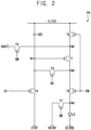
- FIG. 2 is a circuit diagram showing a pixel PX included in the display device 100 of FIG. 1 .
- the pixel PX may include a first transistor T1, a second transistor T2, a third transistor T3, a fourth transistor T4, a fifth transistor T5, a sixth transistor T6, a seventh transistor T7, a storage capacitor CST, and a light emitting diode LE.
- the gate signal (GS in FIG. 1 ) may include a first gate signal GW (or write gate signal), a second gate signal GC (or compensation gate signal), a third gate signal GI (or initialization gate signal), and a fourth gate signal GB (or bypass gate signal).
- the first transistor T1 may include a gate electrode connected to a first node N1, a first electrode connected to a second node N2, and a second electrode connected to a third node N3.
- the first transistor T1 may be referred as a driving transistor.
- the second transistor T2 may include a gate electrode that receives the first gate signal GW, a first electrode that receives the data voltage VDAT, and a second electrode connected to the second node N2.
- the second transistor T2 may be referred as a write transistor.
- the third transistor T3 may include a gate electrode that receives the second gate signal GC, a first electrode connected to the third node N3, and a second electrode connected to the first node N1.
- the third transistor T3 may be referred as a compensation transistor.
- the fourth transistor T4 may include a gate electrode that receives the third gate signal GI, a first electrode that receives a first initialization voltage VINT, and a second electrode connected to the first node N1.
- the fourth transistor T4 may be referred as an initialization transistor.
- the fifth transistor T5 may include a gate electrode that receives the emission signal EM, a first electrode that receives a first power voltage ELVDD, and a second electrode connected to the second node N2.
- the fifth transistor T5 may be referred to as a first light emitting transistor.
- the sixth transistor T6 may include a gate electrode that receives the emission signal EM, a first electrode connected to the third node N3, and a second electrode connected to a fourth node N4.
- the sixth transistor T6 may be referred to as a second light emitting transistor.
- the seventh transistor T7 may include a gate electrode that receives the fourth gate signal GB, a first electrode that receives a second initialization voltage VAINT, and a second electrode connected to the fourth node N4.
- the seventh transistor T7 may be referred as a bypass transistor.
- FIG. 2 shows an embodiment in which each of the first transistor T1, the second transistor T2, the third transistor T3, the fourth transistor T4, the fifth transistor T5, the sixth transistor T6, and the seventh transistor T7 is a P-type transistor (e.g., PMOS transistor), but the present disclosure is not limited thereto.
- at least one of the first transistor T1, the second transistor T2, the third transistor T3, the fourth transistor T4, the fifth transistor T5, the sixth transistor T6, and the seventh transistor T7 may be an N-type transistor (e.g., NMOS transistor).
- the storage capacitor CST may include a first electrode connected to the first node N1 and a second electrode that receives the first power voltage ELVDD.
- FIG. 2 shows that the pixel PX includes seven transistors T1, T2, T3, T4, T5, T6, and T7 and one capacitor CST, but the present disclosure is not limited thereto.
- the pixel PX may include 2 to 6 transistors, 8 or more transistors, and/or 2 or more capacitors.
- the light emitting diode LE may include a first electrode (or anode) connected to the fourth node N4 and a second electrode (or cathode) that receives a second power voltage ELVSS.
- the light emitting diode LE may be an organic light emitting diode.
- the light emitting diode LE may be, for example, an inorganic light emitting diode, a quantum-dot light emitting diode, or a micro light emitting diode.
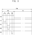
- FIG. 3 is a timing diagram showing signals provided to the pixel PX of FIG. 2 .
- a frame period FRM in which one frame of an image is displayed may include at least one non-emission period PNE and at least one emission period PE.
- the non-emission period PNE may be defined by a turn-off voltage (e.g., logic high voltage) of the emission signal EM
- the emission period PE may be defined by a turn-on voltage (e.g., logic low voltage) of the emission signal EM.
- the light emitting diode LE does not emit light.
- the non-emission period PNE may include a first period P1 (or initialization period), a second period P2 (or compensation and writing period), and a third period P3 (or bypass period).
- the fourth transistor T4 may be turned on in response to a turn-on voltage of the third gate signal GI, and the first initialization voltage VINT may be applied to the first node N1. Accordingly, the first node N1 may be initialized.
- the third transistor T3 may be turned on in response to a turn-on voltage of the second gate signal GC, and the first transistor T1 may be diode-connected. Further, the second transistor T2 may be turned on in response to a turn-on voltage of the first gate signal GW, and the data voltage VDAT for which a threshold voltage of the first transistor T1 is compensated may be applied to the first node N1. Accordingly, the data voltage VDAT for which the threshold voltage of the first transistor T1 is compensated may be written to the first node N1.
- the seventh transistor T7 may be turned on in response to a turn-on voltage of the fourth gate signal GB, and the second initialization voltage VAINT may be applied to the fourth node N4. Accordingly, the fourth node N4 may be initialized.
- the light emitting diode LE may emit light in the emission period PE.
- the fifth transistor T5 and the sixth transistor T6 may be turned on in response to the turn-on voltage of the emission signal EM in the emission period PE, and a current path of a driving current generated in the first transistor T1 may be formed from the first power voltage ELVDD to the second power voltage ELVSS. Accordingly, the light emitting diode LE may emit light with a luminance corresponding to the driving current.
- FIG. 4 is a block diagram showing a luminance controller 152 included in the controller 150 of FIG. 1 .
- a luminance controller 152 may determine a luminance LUM of an image based on the input grayscale values of the input image data IMD1 and a dimming level DBV, and determine an emission-off ratio AOR and an emission cycle CYC based on the luminance LUM of the image.
- the luminance LUM of the image may be determined based on the dimming level DBV
- the dimming level DBV may be set by a user or set by detecting an ambient illuminance.
- the luminance controller 152 may receive the dimming level DBV from a host.
- the emission-off ratio AOR may be a ratio of the sum of non-emission periods to one frame period.
- the emission-off ratio AOR may be a value obtained by dividing the frame period (FRM in FIG. 3 ) including the non-emission periods (PNE in FIG. 3 ) and the emission periods (PE in FIG. 3 ) by the sum of the non-emission periods PNE.
- the emission cycle CYC may correspond to the number of discontinuous emission periods during one frame period.
- the emission cycle CYC may correspond to the number of pulses defined by a falling edge, a turn-on voltage, and a rising edge of the emission signal (EM in FIG. 3 ) within the frame period FRM.
- the controller 150 may generate the emission start signal included in the third control signal CNT3 based on the emission-off ratio AOR and the emission cycle CYC, and the emission driver 140 may generate the emission signal EM based on the third control signal CNT3.
- FIG. 5 is a view for describing a data dimming scheme.
- the luminance controller 152 may control the luminance LUM by changing the data voltage VDAT while maintaining the emission-off ratio AOR constant. Controlling the luminance LUM by changing the data voltage VDAT while maintaining the emission-off ratio AOR constant may be referred as a data dimming scheme.
- the emission cycle CYC may be 1.
- the emission-off ratio AOR may be a minimum emission-off ratio. For example, the minimum emission-off ratio may be 1%.
- the first luminance range may be about 500 nits to about 110 nits.
- the luminance controller 152 may set the data voltage VDAT to a first data voltage VDAT1 while maintaining the emission-off ratio AOR at the minimum emission-off ratio in the first frame period FRM1.
- the luminance controller 152 may set the data voltage VDAT to a second data voltage VDAT2 while maintaining the emission-off ratio AOR at the minimum emission-off ratio in the second frame period FRM2.
- a magnitude of the second data voltage VDAT2 may be less than a magnitude of the first data voltage VDAT1. Accordingly, the second luminance LUM2 of the image in the second frame period FRM2 may be lower than the first luminance LUM1 of the image in the first frame period FRM1.
- FIG. 6 is a view for describing a pulse width modulation (PWM) dimming scheme.
- PWM pulse width modulation
- the luminance controller 152 may control the luminance LUM by changing the emission-off ratio AOR while maintaining the data voltage VDAT constant. Controlling the luminance LUM by changing the emission-off ratio AOR while maintaining the data voltage VDAT constant may be referred as a PWM dimming scheme.
- the emission cycle CYC may be 1.
- the second luminance range may be from about 110 nits to about 80 nits
- the third luminance range may be from about 80 nits to about 0 nits.
- the luminance controller 152 may increase the emission-off ratio AOR while maintaining the data voltage VDAT at the third data voltage VDAT3 of the third frame period FRM3 in the fourth frame period FRM4. In other words, the luminance controller 152 may increase a length of the non-emission period PNE in the fourth frame period FRM4.
- the emission-off ratio AOR (or a length of the non-emission period PNE) in the fourth frame period FRM4 may be greater than the emission-off ratio AOR (or the non-emission period PNE) in the third frame period FRM3. Accordingly, the fourth luminance LUM4 of the image in the fourth frame period FRM4 may be lower than the third luminance LUM3 of the image in the third frame period FRM3.
- the luminance controller 152 may increase the emission-off ratio AOR while maintaining the data voltage VDAT at the third data voltage VDAT3 in the fifth frame period FRM5. In other words, the luminance controller 152 may increase the sum of lengths of the non-emission periods PNE in the fifth frame period FRM5. Further, the luminance controller 152 may increase the emission cycle CYC in the fifth frame period FRM5. When the luminance LUM is included in the third luminance range, the emission cycle CYC may be greater than 1.
- the emission-off ratio AOR (or the sum of the lengths of the non-emission periods PNE) in the fifth frame period FRM5 may be greater than the emission-off ratio AOR (or the length of the non-emission period PNE) in the fourth frame period FRM4, and the emission cycle CYC in the fifth frame period FRM5 may be greater than the emission cycle CYC in the fourth frame period FRM4. Accordingly, the fifth luminance LUM5 of the image in the fifth frame period FRM5 may be lower than the fourth luminance LUM4 of the image in the fourth frame period FRM4.
- the emission cycle CYC may increase in the fifth frame period FRM5 in which the image having the fifth luminance LUM5 included in the third luminance range, which is a low luminance range, is displayed, and a flicker may be prevented from being recognized in a low luminance image.
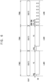
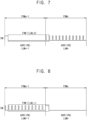
- FIGS. 7 and 8 are views for describing a change in emission cycle CYC according to a comparative example.
- the emission cycle CYC changes between an n-1 th (where n is a positive integer greater than 1) frame period FRMn-1 and an n th frame period FRMn
- the emission-off ratio AOR of the n-1 th frame period FRMn-1 and the emission-off ratio AOR of the n th frame period FRMn may be equal, and the emission cycle CYC of the n-1 th frame period FRMn-1 and the emission cycle CYC of the n th frame period FRMn may be different.
- the emission-off ratio AOR of the n-1 th frame period FRMn-1 and the emission-off ratio AOR of the n th frame period FRMn may be 12%.
- the luminance LUMn-1 of the n-1 th frame period FRMn-1 and the luminance LUMn of the n th frame period FRMn may be equal.
- the luminance LUMn-1 of the n-1 th frame period FRMn-1 and the luminance LUMn of the n th frame period FRMn may be about 80 nits.
- a frame corresponding period FRM' corresponding to the length of one frame period and including emission periods with the sum of lengths greater than the sum of the length of the emission period of the n-1 th frame period FRMn-1 and the lengths of the emission periods of the n th frame period FRMn may exist, and the luminance LUM_H of the frame corresponding period FRM' may be higher than the luminance LUMn-1 of the n-1 th frame period FRMn-1 and the luminance LUMn of the n th frame period FRMn.
- the luminance LUM_H of the frame corresponding period FRM' may be about 81 nits.
- flashing corresponding to an increase in luminance of the image may occur between the n-1 th frame period FRMn-1 and the n th frame period FRMn.
- a frame corresponding period FRM' corresponding to the length of one frame period and including emission periods with the sum of lengths less than the sum of the lengths of the emission periods of the n-1 th frame period FRMn-1 and the length of the emission period of the n th frame period FRMn may exist, and the luminance LUM_H of the frame corresponding period FRM' may be lower than the luminance LUMn-1 of the n-1 th frame period FRMn-1 and the luminance LUMn of the n th frame period FRMn.
- the luminance LUM_H of the frame corresponding period FRM' may be about 79 nits.
- flashing corresponding to a decrease in luminance of the image may occur between the n-1 th frame period FRMn-1 and the n th frame period FRMn.
- the emission cycle CYC of one of the n-1 th frame period FRMn-1 and the n+1 th frame period FRMn+1 may be 1, and the emission cycle CYC of another of the n-1 th frame period FRMn-1 and the n+1 th frame period FRMn+1 may be 12, 16, 24, or 32.
- An embodiment in which the emission cycle CYC of the frame period with the larger emission cycle CYC among the n-1 th frame period FRMn-1 and the n+1 th frame period FRMn+1 is 12 is shown in FIGS.
- the present disclosure is not limited thereto.
- the emission cycle CYC of the frame period with the larger emission cycle CYC among the n-1 th frame period FRMn-1 and the n+1 th frame period FRMn+1 may be 16, 24, or 32.
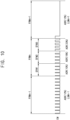
- the n th frame period FRMn (or buffer frame period) between the n-1 th frame period FRMn-1 and the n+1 th frame period FRMn+1 in which the emission cycles CYC are different and the emission-off ratios AOR are equal may include first to m th (where m is a positive integer greater than 1) sub-frame periods having different emission-off ratios AOR.
- the emission-off ratio AOR of the n-1 th frame period FRMn-1 and the emission-off ratio AOR of the n+1 th frame period FRMn+1 may be 12%.
- the luminance LUMn-1 of the n-1 th frame period FRMn-1 and the luminance LUMn+1 of the n+1 th frame period FRMn+1 may be equal.
- the luminance LUMn-1 of the n-1 th frame period FRMn-1 and the luminance LUMn+1 of the n+1 th frame period FRMn+1 may be about 80 nits.
- the emission cycle CYC of the n th frame period FRMn may be equal to the emission cycle CYC of the frame period with the larger emission cycle CYC among the n-1 th frame period FRMn-1 and the n+1 th frame period FRMn+1.
- the emission cycle CYC of the n th frame period FRMn may be 12.
- the n th frame period FRMn may include three first to third sub-frame periods SFM1, SFM2, and SFM3.
- the present disclosure is not limited thereto.
- the n th frame period FRMn may include two or four or more sub-frame periods.
- the emission-off ratios AOR may decrease from the first sub-frame period to the m th sub-frame period.
- the emission-off ratio AOR of the second sub-frame period SFM2 may be less than the emission-off ratio AOR of the first sub-frame period SFM1
- the emission-off ratio AOR of the third sub-frame period SFM3 may be less than the emission-off ratio AOR of the second sub-frame period SFM2.
- the emission-off ratio AOR of the first sub-frame period may be greater than the emission-off ratio AOR of the n-1 th frame period FRMn-1. Further, the emission-off ratio AOR of the m th sub-frame period may be less than the emission-off ratio AOR of the n+1 th frame period FRMn+1.
- the emission-off ratio AOR of the first sub-frame period SFM1 may be 23%
- the emission-off ratio AOR of the second sub-frame period SFM2 may be 19%
- the emission-off ratio AOR of the third sub-frame period SFM3 may be 10%.
- the emission-off ratios AOR may increase from the first sub-frame period to the m th sub-frame period.
- the emission-off ratio AOR of the second sub-frame period SFM2 may be greater than the emission-off ratio AOR of the first sub-frame period SFM1
- the emission-off ratio AOR of the third sub-frame period SFM3 may be greater than the emission-off ratio AOR of the second sub-frame period SFM2.
- the emission-off ratio AOR of the m th sub-frame period may be greater than the emission-off ratio AOR of the n+1 th frame period FRMn+1. Further, the emission-off ratio AOR of the first sub-frame period may be less than the emission-off ratio AOR of the n-1 th frame period FRMn-1.
- the emission-off ratio AOR of the first sub-frame period SFM1 may be 10%
- the emission-off ratio AOR of the second sub-frame period SFM2 may be 19%
- the emission-off ratio AOR of the third sub-frame period SFM3 may be 23%.
- the buffer frame FRMn including the sub-frames (sub-frame periods SFM) having different emission-off ratios AOR may be inserted between the n-1 th frame period FRMn-1 and the n+1 th frame period FRMn+1.
- flashing may be prevented from occurring when the emission cycle CYC changes.
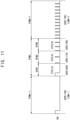
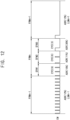
- FIGS. 11 and 12 are views for describing a change in emission cycle CYC according to an embodiment.
- the emission-off ratios AOR of the first to m th sub-frame periods may be different, and the emission cycles CYC of the first to m th sub-frame periods may be different.
- the emission cycle CYC of the n th frame period FRMn may be between the emission cycle CYC of the n-1 th frame period FRMn-1 and the emission cycle CYC of the n+1 th frame period FRMn+1.
- the emission cycle CYC of the n th frame period FRMn may be greater than 1 and less than 12.
- the emission-off ratios AOR may decrease and the emission cycles CYC may increase from the first sub-frame period to the m th sub-frame period.
- the emission cycle CYC of the second sub-frame period SFM2 may be greater than the emission cycle CYC of the first sub-frame period SFM1
- the emission cycle CYC of the third sub-frame period SFM3 may be greater than the emission cycle CYC of the second sub-frame period SFM2.
- the emission cycle CYC of the sub-frame period may be a value obtained by multiplying the number of discontinuous emission periods included in the sub-frame period by the number of sub-frame periods included in the n th frame period FRMn.
- the emission-off ratio AOR of the first sub-frame period may be greater than the emission-off ratio AOR of the n-1 th frame period FRMn-1, and the emission-off ratio AOR of the m th sub-frame period may be less than the emission-off ratio AOR of the n+1 th frame period FRMn+1.
- the emission cycle CYC of the first sub-frame period may be greater than the emission cycle CYC of the n-1 th frame period FRMn-1, and the emission cycle CYC of the m th sub-frame period may be less than the emission cycle CYC of the n+1 th frame period FRMn+1.
- the emission-off ratio AOR of the first sub-frame period SFM1 may be 30%
- the emission-off ratio AOR of the second sub-frame period SFM2 may be 11%
- the emission-off ratio AOR of the third sub-frame period SFM3 may be 10%.
- the emission cycle CYC of the first sub-frame period SFM1 may be 3, the emission cycle CYC of the second sub-frame period SFM2 may be 6, and the emission cycle CYC of the third sub-frame period SFM3 may be 9.
- the emission-off ratios AOR may increase and the emission cycles CYC may decrease from the first sub-frame period to the m th sub-frame period.
- the emission cycle CYC of the second sub-frame period SFM2 may be less than the emission cycle CYC of the first sub-frame period SFM1
- the emission cycle CYC of the third sub-frame period SFM3 may be less than the emission cycle CYC of the second sub-frame period SFM2.
- the emission-off ratio AOR of the first sub-frame period may be less than the emission-off ratio AOR of the n-1 th frame period FRMn-1, and the emission-off ratio AOR of the m th sub-frame period may be greater than the emission-off ratio AOR of the n+1 th frame period FRMn+1.
- the emission cycle CYC of the first sub-frame period may be less than the emission cycle CYC of the n-1 th frame period FRMn-1
- the emission cycle CYC of the m th sub-frame period may be greater than the emission cycle CYC of the n+1 th frame period FRMn+1.
- the emission-off ratio AOR of the first sub-frame period SFM1 may be 10%
- the emission-off ratio AOR of the second sub-frame period SFM2 may be 11%
- the emission-off ratio AOR of the third sub-frame period SFM3 may be 30%.
- the emission cycle CYC of the first sub-frame period SFM1 may be 9, the emission cycle CYC of the second sub-frame period SFM2 may be 6, and the emission cycle CYC of the third sub-frame period SFM3 may be 3.
- the buffer frame FRMn including the sub-frames (sub-frame periods SFM) having different emission-off ratios AOR and different emission cycles CYC may be inserted between the n-1 th frame period FRMn-1 and the n+1 th frame period FRMn+1.
- flashing may be prevented from occurring when the emission cycle CYC changes.
- FIGS. 13 and 14 are views for describing a change in emission cycle CYC according to an embodiment.
- the emission cycle CYC of one of the n-1 th frame period FRMn-1 and the n th frame period FRMn may be 1, and the emission cycle CYC of another of the n-1 th frame period FRMn-1 and the n th frame period FRMn may be 12, 16, 24, or 32.
- An embodiment in which the emission cycle CYC of the frame period with the larger emission cycle CYC among the n-1 th frame period FRMn-1 and the n th frame period FRMn is 12 is shown in FIGS. 13 and 14 , but the present disclosure is not limited thereto.
- the emission cycle CYC of the frame period with the larger emission cycle CYC among the n-1 th frame period FRMn-1 and the n th frame period FRMn may be 16, 24, or 32.
- the luminance LUMn-1 of the n-1 th frame period FRMn-1 and the luminance LUMn of the n th frame period FRMn may be equal.
- the luminance LUMn-1 of the n-1 th frame period FRMn-1 and the luminance LUMn of the n th frame period FRMn may be about 80 nits.
- the length of the non-emission period PNE of a first frame period may be substantially equal to the length of the non-emission period PNE of a second frame period (another of the n-1 th frame period FRMn-1 and the n th frame period FRMn) adjacent to the first frame period.
- FIG. 13 shows that the first frame period and the second frame period are the n-1 th frame period FRMn-1 and the n th frame period FRMn, respectively
- FIG. 14 shows that the first frame period and the second frame period are the n th frame period FRMn and the n-1 th frame period FRMn-1, respectively.
- the first frame period may have a first emission cycle and a first emission-off ratio
- the second frame period may have a second emission cycle greater than the first emission cycle and a second emission-off ratio greater than the first emission-off ratio.
- the first emission-off ratio may be the minimum emission-off ratio.
- the emission-off ratio AOR of the n-1 th frame period FRMn-1 may be the minimum emission-off ratio, and the magnitude of the data voltage VDATn-1 of the n-1 th frame period FRMn-1 may be less than the magnitude of the data voltage VDATn of the n th frame period FRMn.
- the emission-off ratio AOR of the n-1 th frame period FRMn-1 may be 1%, and the emission-off ratio AOR of the n th frame period FRMn may be 12%.
- the emission-off ratio AOR of the n th frame period FRMn may be the minimum emission-off ratio, and the magnitude of the data voltage VDATn of the n th frame period FRMn may be less than the magnitude of the data voltage VDATn-1 of the n-1 th frame period FRMn-1.
- the emission-off ratio AOR of the n-1 th frame period FRMn-1 may be 12%, and the emission-off ratio AOR of the n th frame period FRMn may be 1%.
- the length of the one non-emission period PNE of the n-1 th frame period FRMn-1 and the length of the one non-emission period PNE of the n th frame period FRMn may be substantially equal, and the length of the first non-emission period PNE of the n-1 th frame period FRMn-1 and the length of the first non-emission period PNE of the n th frame period FRMn may be substantially equal.
- flashing may be prevented from occurring when the emission cycle CYC changes.
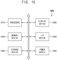
- FIG. 15 is a block diagram showing an electronic apparatus 1000 according to an embodiment.
- an electronic apparatus 1000 may include a processor 1010, a memory device 1020, a storage device 1030, an input/output ("I/O") device 1040, a power supply 1050, and a display device 1060.
- the display device 1060 may correspond to the display device 100 in FIG. 1 .
- the electronic apparatus 1000 may further include a plurality of ports for communicating with, for example, a video card, a sound card, a memory card, a universal serial bus (“USB”) device, etc.
- USB universal serial bus
- the processor 1010 may perform calculations or tasks.
- the processor 1010 may be, for example, a microprocessor, a central processing unit ("CPU"), or the like.
- the processor 1010 may be coupled to other components via, for example, an address bus, a control bus, a data bus, or the like.
- the processor 1010 may be coupled to an extended bus such as a peripheral component interconnection ("PCI") bus.
- the processor 1010 may provide input image data (e.g., IMD1 in FIG. 1 ) and a control signal (e.g., CNT in FIG. 1 ) to the display device 1060.
- IMD1 input image data
- a control signal e.g., CNT in FIG. 1
- the memory device 1020 may store data for operations of the electronic apparatus 1000.
- the memory device 1020 may include a non-volatile memory device such as, for example, an erasable programmable read-only memory (“EPROM”) device, an electrically erasable programmable read-only memory (“EEPROM”) device, a flash memory device, a phase change random access memory (“PRAM”) device, a resistance random access memory (“RRAM”) device, a nano floating gate memory (“NFGM”) device, a polymer random access memory (“PoRAM”) device, a magnetic random access memory (“MRAM”) device, a ferroelectric random access memory (“FRAM”) device, etc., and/or a volatile memory device such as, for example, a dynamic random access memory (“DRAM”) device, a static random access memory (“SRAM”) device, a mobile DRAM device, etc.
- DRAM dynamic random access memory
- SRAM static random access memory
- the storage device 1030 may include, for example, a solid-state drive (“SSD”) device, a hard disk drive (“HDD”) device, a CD-ROM device, or the like.
- the I/O device 1040 may include an input device such as, for example, a keyboard, a keypad, a touchpad, a touchscreen, a mouse device, etc., and an output device such as, for example, a speaker, a printer, etc.
- the power supply 1050 may supply power utilized for the operation of the electronic apparatus 1000.
- the display device 1060 may be coupled to other components via the buses or other communication links.
- the display device may be applied to a display device included in, for example, a computer, a notebook, a mobile phone, a smart phone, a smart pad, a smart watch, a PMP, a PDA, an MP3 player, or the like.
- each block, unit and/or module may be implemented by dedicated hardware, or as a combination of dedicated hardware to perform some functions and a processor (e.g., one or more programmed microprocessors and associated circuitry) to perform other functions.
Landscapes
- Engineering & Computer Science (AREA)
- Physics & Mathematics (AREA)
- Computer Hardware Design (AREA)
- General Physics & Mathematics (AREA)
- Theoretical Computer Science (AREA)
- Multimedia (AREA)
- Control Of Indicators Other Than Cathode Ray Tubes (AREA)
Abstract
Description
- Embodiments of the present disclosure relate to a display device. More particularly, embodiments of the present disclosure relate to a display device having improved image quality.
- A display device may display images having different luminances for frame periods. A frame period may include at least one emission period, and a pixel included in the display device may emit light in the emission period.
- An emission cycle corresponding to the number of discontinuous emission periods during one frame period may be changed between adjacent frame periods. When the emission cycle is changed, flashing in which a luminance of an image displayed by the display device momentarily increases or decreases may occur. When this flashing occurs in the image, an image quality of the display device may deteriorate.
- Embodiments of the present disclosure provide a display device having improved image quality.
- A display device according to embodiments of the present disclosure includes a display panel including a pixel and an emission line connected to the pixel, and an emission driver which provides an emission signal to the emission line. The emission signal defines discontinuous emission periods and non-emission periods during a frame period among a plurality of frame periods. The display device further includes a controller which determines an emission cycle corresponding to a number of the discontinuous emission periods during the frame period and an emission-off ratio which is a ratio of a sum of the non-emission periods to the frame period. The plurality of frame periods includes an n-1th frame period, an n+1th frame period, and an nth frame period between the n-1th frame period and the n+1th frame period. The emission cycle of the n-1th frame period is different from the emission cycle of the n+1th frame period, the emission-off ratio of the n-1th frame period is equal to the emission-off ratio of the n+1th frame period, and the nth frame period includes first to mth sub-frame periods having different emission-off ratios. Each of m and n is a positive integer greater than 1.
- In an embodiment, the emission-off ratios of the first to mth sub-frame periods may decrease from the first sub-frame period to the mth sub-frame period when the emission cycle of the n+1th frame period is greater than the emission cycle of the n-1th frame period.
- In an embodiment, the emission-off ratio of the first sub-frame period may be greater than the emission-off ratio of the n-1th frame period.
- In an embodiment, the emission-off ratios of the first to mth sub-frame periods may increase from the first sub-frame period to the mth sub-frame period when the emission cycle of the n+1th frame period is less than the emission cycle of the n-1th frame period.
- In an embodiment, the emission-off ratio of the mth sub-frame period may be greater than the emission-off ratio of the n+1th frame period.
- In an embodiment, the emission cycle of the nth frame period may be equal to the emission cycle of a frame period with the greater emission cycle among the n-1th frame period and the n+1th frame period.
- In an embodiment, emission cycles of the first to mth sub-frames (first to mth sub-frame periods) may be different.
- In an embodiment, the emission cycles may increase from the first sub-frame period to the mth sub-frame period when the emission cycle of the n+1th frame period is greater than the emission cycle of the n-1th frame period.
- In an embodiment, the emission-off ratio of the first sub-frame period may be greater than the emission-off ratio of the n-1th frame period.
- In an embodiment, the emission cycle of the first sub-frame period may be greater than the emission cycle of the n-1th frame period, and the emission cycle of the mth sub-frame period may be less than the emission cycle of the n+1th frame period.
- In an embodiment, the emission cycles of the first to mth sub-frame periods may decrease from the first sub-frame period to the mth sub-frame period when the emission cycle of the n+1th frame period is less than the emission cycle of the n-1th frame period.
- In an embodiment, the emission-off ratio of the mth sub-frame period may be greater than the emission-off ratio of the n+1th frame period.
- In an embodiment, the emission cycle of the first sub-frame period may be less than the emission cycle of the n-1th frame period, and the emission cycle of the mth sub-frame period may be greater than the emission cycle of the n+1th frame period.
- In an embodiment, the emission cycle of the nth frame period may be between the emission cycle of the n-1th frame period and the emission cycle of the n+1th frame period.
- In an embodiment, the emission cycle of one of the n-1th frame period and the n+1th frame period may be 1, and the emission cycle of another of the n-1th frame period and the n+1th frame period may be 12, 16, 24, or 32.
- In an embodiment, luminances of the n-1th and n+1th frame periods may be equal.
- A display device according to embodiments of the present disclosure may include a display panel including a pixel and an emission line connected to the pixel, and an emission driver which provides an emission signal to the emission line. The emission signal may define discontinuous emission periods and non-emission periods during a frame period among a plurality of frame periods. The display device may further include a controller which may determine an emission cycle corresponding to a number of the discontinuous emission periods during the frame period and an emission-off ratio which is a ratio of a sum of the non-emission periods to the frame period. A first frame period may have a first emission cycle, a second frame period adjacent to the first frame period may have a second emission cycle greater than the first emission cycle, and a length of a non-emission period of the first frame period may be equal to a length of a non-emission period of the second frame period.
- In an embodiment, the first frame period may have a first emission-off ratio which is a minimum emission-off ratio, and the second frame period may have a second emission-off ratio greater than the first emission-off ratio.
- In an embodiment, a magnitude of a data voltage of the first frame period may be less than a magnitude of a data voltage of the second frame period.
- In an embodiment, the first emission cycle may be 1, and the second emission cycle may be 12, 16, 24, or 32.
- In the display device according to embodiments of the present disclosure, when the emission cycle is changed between the adjacent frame periods, a buffer frame period including sub-frame periods having different emission-off ratios may be inserted between the adjacent frame periods, or lengths of non-emission periods of the adjacent frame periods may be equal. Accordingly, the flashing of the image displayed by the display device may not occur although a difference in the emission cycles between the adjacent frame periods is large.
- All embodiments described in this specification may be advantageously combined with one another to the extent that their respective features are compatible. In particular, the expressions "according to an embodiment," "in an embodiment," "an embodiment of the invention provides" etc. mean that the respective features may or may not be part of specific embodiments of the present invention.
- The above and other features of the present disclosure will become more apparent by describing in detail embodiments thereof with reference to the accompanying drawings.
-
FIG. 1 is a block diagram showing a display device according to an embodiment. -
FIG. 2 is a circuit diagram showing a pixel included in the display device ofFIG. 1 . -
FIG. 3 is a timing diagram showing signals provided to the pixel ofFIG. 2 . -
FIG. 4 is a block diagram showing a luminance controller included in a controller ofFIG. 1 . -
FIG. 5 is a view for describing a data dimming scheme. -
FIG. 6 is a view for describing a pulse width modulation (PWM) dimming scheme. -
FIGS. 7 and 8 are views for describing a change in emission cycle according to a comparative example. -
FIGS. 9 and10 are views for describing a change in emission cycle according to an embodiment. -
FIGS. 11 and12 are views for describing a change in emission cycle according to an embodiment. -
FIGS. 13 and 14 are views for describing a change in emission cycle according to an embodiment. -
FIG. 15 is a block diagram showing an electronic apparatus according to an embodiment. - Hereinafter, a display device according to embodiments of the present disclosure will be described in more detail with reference to the accompanying drawings. Like reference numerals may refer to like elements throughout the accompanying drawings .
- It will be understood that the terms "first," "second," "third," etc. are used herein to distinguish one element from another, and the elements are not limited by these terms. Thus, a "first" element in an embodiment may be described as a "second" element in another embodiment.
- It should be understood that descriptions of features or aspects within each embodiment should typically be considered as available for other similar features or aspects in other embodiments, unless the context clearly indicates otherwise.
- As used herein, the singular forms "a", "an" and "the" are intended to include the plural forms as well, unless the context clearly indicates otherwise.
- Herein, when two or more elements or values are described as being substantially the same as or about equal to each other, it is to be understood that the elements or values are identical to each other, the elements or values are equal to each other within a measurement error, or if measurably unequal, are close enough in value to be functionally equal to each other as would be understood by a person having ordinary skill in the art. For example, the term "about" as used herein is inclusive of the stated value and means within an acceptable range of deviation for the particular value as determined by one of ordinary skill in the art, considering the measurement in question and the error associated with measurement of the particular quantity (e.g., the limitations of the measurement system). For example, "about" may mean within one or more standard deviations as understood by one of the ordinary skill in the art. Further, it is to be understood that while parameters may be described herein as having "about" a certain value, according to embodiments, the parameter may be exactly the certain value or approximately the certain value within a measurement error as would be understood by a person having ordinary skill in the art.
-
FIG. 1 is a block diagram showing adisplay device 100 according to an embodiment. - Referring to
FIG. 1 , adisplay device 100 may include adisplay panel 110, a gate driver 120 (also referred to as a gate driver circuit), a data driver 130 (also referred to as a data driver circuit), an emission driver 140 (also referred to as an emission driver circuit), and a controller 150 (also referred to as a controller circuit). - The
display panel 110 may include a plurality of pixels PX, a plurality of gate lines GL, a plurality of data lines DL, and a plurality of emission lines EML. - The pixels PX may include pixels that emit light of multiple colors. In an embodiment, the pixels PX may include red pixels that emit red light, green pixels that emit green light, and blue pixels that emit blue light.
- The gate lines GL may be connected to the pixels PX. The gate lines GL may extend in a first direction D1 and be arranged in a second direction D2 crossing the first direction D1. The gate lines GL may provide gate signals GS to the pixels PX.
- The data lines DL may be connected to the pixels PX. The data lines DL may extend in the second direction D2 and be arranged in the first direction D1. The data lines DL may provide data voltages VDAT to the pixels PX.
- The emission lines EML may be connected to the pixels PX. The emission lines EML may extend in the first direction D1 and be arranged in the second direction D2. The emission lines EML may provide emission signals EM to the pixels PX.
- The
gate driver 120 may provide the gate signals GS to the gate lines GL. Thegate driver 120 may generate the gate signals GS based on a first control signal CNT1. The first control signal CNT1 may include, for example, a gate start signal, a gate clock signal, etc. - The
data driver 130 may provide the data voltages VDAT to the data lines DL. Thedata driver 130 may generate the data voltages VDAT based on output image data IMD2 and a second control signal CNT2. The output image data IMD2 may include output grayscale values corresponding to the pixels PX. The second control signal CNT2 may include, for example, a load signal, a data clock signal, etc. - The
emission driver 140 may provide the emission signals EM to the emission lines EML. Theemission driver 140 may generate the emission signals EM based on a third control signal CNT3. The third control signal CNT3 may include, for example, an emission start signal, an emission clock signal, etc. - The
controller 150 may control an operation (or driving) of thegate driver 120, an operation (or driving) of thedata driver 130, and an operation (or driving) of theemission driver 140. Thecontroller 150 may receive input image data IMD1 and a control signal CNT from a host (e.g., processor). The input image data IMD1 may include input grayscale values corresponding to the pixels PX. The control signal CNT may include, for example, a clock signal, a vertical synchronization signal, a horizontal synchronization signal, a data enable signal, etc. Thecontroller 150 may provide the first control signal CNT1 to thegate driver 120, provide the output image data IMD2 and the second control signal CNT2 to thedata driver 130, and provide the third control signal CNT3 to theemission driver 140. Thecontroller 150 may generate the first to third control signals CNT1, CNT2, and CNT3 based on the control signal CNT, and generate the output image data IMD2 based on the input image data IMD1. -
FIG. 2 is a circuit diagram showing a pixel PX included in thedisplay device 100 ofFIG. 1 . - Referring to
FIG. 2 , the pixel PX may include a first transistor T1, a second transistor T2, a third transistor T3, a fourth transistor T4, a fifth transistor T5, a sixth transistor T6, a seventh transistor T7, a storage capacitor CST, and a light emitting diode LE. The gate signal (GS inFIG. 1 ) may include a first gate signal GW (or write gate signal), a second gate signal GC (or compensation gate signal), a third gate signal GI (or initialization gate signal), and a fourth gate signal GB (or bypass gate signal). - The first transistor T1 may include a gate electrode connected to a first node N1, a first electrode connected to a second node N2, and a second electrode connected to a third node N3. The first transistor T1 may be referred as a driving transistor.
- The second transistor T2 may include a gate electrode that receives the first gate signal GW, a first electrode that receives the data voltage VDAT, and a second electrode connected to the second node N2. The second transistor T2 may be referred as a write transistor.
- The third transistor T3 may include a gate electrode that receives the second gate signal GC, a first electrode connected to the third node N3, and a second electrode connected to the first node N1. The third transistor T3 may be referred as a compensation transistor.
- The fourth transistor T4 may include a gate electrode that receives the third gate signal GI, a first electrode that receives a first initialization voltage VINT, and a second electrode connected to the first node N1. The fourth transistor T4 may be referred as an initialization transistor.
- The fifth transistor T5 may include a gate electrode that receives the emission signal EM, a first electrode that receives a first power voltage ELVDD, and a second electrode connected to the second node N2. The fifth transistor T5 may be referred to as a first light emitting transistor.
- The sixth transistor T6 may include a gate electrode that receives the emission signal EM, a first electrode connected to the third node N3, and a second electrode connected to a fourth node N4. The sixth transistor T6 may be referred to as a second light emitting transistor.
- The seventh transistor T7 may include a gate electrode that receives the fourth gate signal GB, a first electrode that receives a second initialization voltage VAINT, and a second electrode connected to the fourth node N4. The seventh transistor T7 may be referred as a bypass transistor.
-
FIG. 2 shows an embodiment in which each of the first transistor T1, the second transistor T2, the third transistor T3, the fourth transistor T4, the fifth transistor T5, the sixth transistor T6, and the seventh transistor T7 is a P-type transistor (e.g., PMOS transistor), but the present disclosure is not limited thereto. For example, in an embodiment, at least one of the first transistor T1, the second transistor T2, the third transistor T3, the fourth transistor T4, the fifth transistor T5, the sixth transistor T6, and the seventh transistor T7 may be an N-type transistor (e.g., NMOS transistor). - The storage capacitor CST may include a first electrode connected to the first node N1 and a second electrode that receives the first power voltage ELVDD.
-
FIG. 2 shows that the pixel PX includes seven transistors T1, T2, T3, T4, T5, T6, and T7 and one capacitor CST, but the present disclosure is not limited thereto. For example, in an embodiment, the pixel PX may include 2 to 6 transistors, 8 or more transistors, and/or 2 or more capacitors. - The light emitting diode LE may include a first electrode (or anode) connected to the fourth node N4 and a second electrode (or cathode) that receives a second power voltage ELVSS. In an embodiment, the light emitting diode LE may be an organic light emitting diode. In an embodiment, the light emitting diode LE may be, for example, an inorganic light emitting diode, a quantum-dot light emitting diode, or a micro light emitting diode.
-
FIG. 3 is a timing diagram showing signals provided to the pixel PX ofFIG. 2 . - Referring to
FIGS. 2 and3 , a frame period FRM in which one frame of an image is displayed may include at least one non-emission period PNE and at least one emission period PE. The non-emission period PNE may be defined by a turn-off voltage (e.g., logic high voltage) of the emission signal EM, and the emission period PE may be defined by a turn-on voltage (e.g., logic low voltage) of the emission signal EM. - In an embodiment, in the non-emission period PNE, the light emitting diode LE does not emit light. The non-emission period PNE may include a first period P1 (or initialization period), a second period P2 (or compensation and writing period), and a third period P3 (or bypass period).
- In the first period P1, the fourth transistor T4 may be turned on in response to a turn-on voltage of the third gate signal GI, and the first initialization voltage VINT may be applied to the first node N1. Accordingly, the first node N1 may be initialized.
- In the second period P2, the third transistor T3 may be turned on in response to a turn-on voltage of the second gate signal GC, and the first transistor T1 may be diode-connected. Further, the second transistor T2 may be turned on in response to a turn-on voltage of the first gate signal GW, and the data voltage VDAT for which a threshold voltage of the first transistor T1 is compensated may be applied to the first node N1. Accordingly, the data voltage VDAT for which the threshold voltage of the first transistor T1 is compensated may be written to the first node N1.
- In the third period P3, the seventh transistor T7 may be turned on in response to a turn-on voltage of the fourth gate signal GB, and the second initialization voltage VAINT may be applied to the fourth node N4. Accordingly, the fourth node N4 may be initialized.
- The light emitting diode LE may emit light in the emission period PE. The fifth transistor T5 and the sixth transistor T6 may be turned on in response to the turn-on voltage of the emission signal EM in the emission period PE, and a current path of a driving current generated in the first transistor T1 may be formed from the first power voltage ELVDD to the second power voltage ELVSS. Accordingly, the light emitting diode LE may emit light with a luminance corresponding to the driving current.
-
FIG. 4 is a block diagram showing aluminance controller 152 included in thecontroller 150 ofFIG. 1 . - Referring to
FIGS. 1 and4 , aluminance controller 152 may determine a luminance LUM of an image based on the input grayscale values of the input image data IMD1 and a dimming level DBV, and determine an emission-off ratio AOR and an emission cycle CYC based on the luminance LUM of the image. - The luminance LUM of the image may be determined based on the dimming level DBV The dimming level DBV may be set by a user or set by detecting an ambient illuminance. For example, the
luminance controller 152 may receive the dimming level DBV from a host. - The emission-off ratio AOR may be a ratio of the sum of non-emission periods to one frame period. For example, the emission-off ratio AOR may be a value obtained by dividing the frame period (FRM in
FIG. 3 ) including the non-emission periods (PNE inFIG. 3 ) and the emission periods (PE inFIG. 3 ) by the sum of the non-emission periods PNE. - The emission cycle CYC may correspond to the number of discontinuous emission periods during one frame period. For example, the emission cycle CYC may correspond to the number of pulses defined by a falling edge, a turn-on voltage, and a rising edge of the emission signal (EM in
FIG. 3 ) within the frame period FRM. - The
controller 150 may generate the emission start signal included in the third control signal CNT3 based on the emission-off ratio AOR and the emission cycle CYC, and theemission driver 140 may generate the emission signal EM based on the third control signal CNT3. -
FIG. 5 is a view for describing a data dimming scheme. - Referring to
FIGS. 4 and 5 , when the luminance LUM of the image is included in a first luminance range (or high luminance range), theluminance controller 152 may control the luminance LUM by changing the data voltage VDAT while maintaining the emission-off ratio AOR constant. Controlling the luminance LUM by changing the data voltage VDAT while maintaining the emission-off ratio AOR constant may be referred as a data dimming scheme. When the luminance LUM is included in the first luminance range, the emission cycle CYC may be 1. In an embodiment, the emission-off ratio AOR may be a minimum emission-off ratio. For example, the minimum emission-off ratio may be 1%. For example, the first luminance range may be about 500 nits to about 110 nits. - When the image has a first luminance LUM1 included in the first luminance range in a first frame period FRM1, the
luminance controller 152 may set the data voltage VDAT to a first data voltage VDAT1 while maintaining the emission-off ratio AOR at the minimum emission-off ratio in the first frame period FRM1. - When the image has a second luminance LUM2 included in the first luminance range and lower than the first luminance LUM1 in a second frame period FRM2, the
luminance controller 152 may set the data voltage VDAT to a second data voltage VDAT2 while maintaining the emission-off ratio AOR at the minimum emission-off ratio in the second frame period FRM2. A magnitude of the second data voltage VDAT2 may be less than a magnitude of the first data voltage VDAT1. Accordingly, the second luminance LUM2 of the image in the second frame period FRM2 may be lower than the first luminance LUM1 of the image in the first frame period FRM1. -
FIG. 6 is a view for describing a pulse width modulation (PWM) dimming scheme. - Referring to
FIGS. 4 and6 , when the luminance LUM of the image is included in a second luminance range (or middle luminance range) or a third luminance range (or low luminance range), theluminance controller 152 may control the luminance LUM by changing the emission-off ratio AOR while maintaining the data voltage VDAT constant. Controlling the luminance LUM by changing the emission-off ratio AOR while maintaining the data voltage VDAT constant may be referred as a PWM dimming scheme. When the luminance LUM is included in the second luminance range, the emission cycle CYC may be 1. For example, the second luminance range may be from about 110 nits to about 80 nits, and the third luminance range may be from about 80 nits to about 0 nits. - When the image has a third luminance LUM3 included in the second luminance range in a third frame period FRM3 and the image has a fourth luminance LUM4 included in the second luminance range and lower than the third luminance LUM3 in a fourth frame period FRM4, the
luminance controller 152 may increase the emission-off ratio AOR while maintaining the data voltage VDAT at the third data voltage VDAT3 of the third frame period FRM3 in the fourth frame period FRM4. In other words, theluminance controller 152 may increase a length of the non-emission period PNE in the fourth frame period FRM4. Accordingly, the emission-off ratio AOR (or a length of the non-emission period PNE) in the fourth frame period FRM4 may be greater than the emission-off ratio AOR (or the non-emission period PNE) in the third frame period FRM3. Accordingly, the fourth luminance LUM4 of the image in the fourth frame period FRM4 may be lower than the third luminance LUM3 of the image in the third frame period FRM3. - When the image has a fifth luminance LUM5 included in the third luminance range and lower than the fourth luminance LUM4 in a fifth frame period FRM5, the
luminance controller 152 may increase the emission-off ratio AOR while maintaining the data voltage VDAT at the third data voltage VDAT3 in the fifth frame period FRM5. In other words, theluminance controller 152 may increase the sum of lengths of the non-emission periods PNE in the fifth frame period FRM5. Further, theluminance controller 152 may increase the emission cycle CYC in the fifth frame period FRM5. When the luminance LUM is included in the third luminance range, the emission cycle CYC may be greater than 1. Accordingly, the emission-off ratio AOR (or the sum of the lengths of the non-emission periods PNE) in the fifth frame period FRM5 may be greater than the emission-off ratio AOR (or the length of the non-emission period PNE) in the fourth frame period FRM4, and the emission cycle CYC in the fifth frame period FRM5 may be greater than the emission cycle CYC in the fourth frame period FRM4. Accordingly, the fifth luminance LUM5 of the image in the fifth frame period FRM5 may be lower than the fourth luminance LUM4 of the image in the fourth frame period FRM4. Further, the emission cycle CYC may increase in the fifth frame period FRM5 in which the image having the fifth luminance LUM5 included in the third luminance range, which is a low luminance range, is displayed, and a flicker may be prevented from being recognized in a low luminance image. -
FIGS. 7 and 8 are views for describing a change in emission cycle CYC according to a comparative example. - Referring to
FIGS. 7 and 8 , in a comparative example, when the emission cycle CYC changes between an n-1th (where n is a positive integer greater than 1) frame period FRMn-1 and an nth frame period FRMn, the emission-off ratio AOR of the n-1th frame period FRMn-1 and the emission-off ratio AOR of the nth frame period FRMn may be equal, and the emission cycle CYC of the n-1th frame period FRMn-1 and the emission cycle CYC of the nth frame period FRMn may be different. For example, the emission-off ratio AOR of the n-1th frame period FRMn-1 and the emission-off ratio AOR of the nth frame period FRMn may be 12%. Further, the luminance LUMn-1 of the n-1th frame period FRMn-1 and the luminance LUMn of the nth frame period FRMn may be equal. For example, the luminance LUMn-1 of the n-1th frame period FRMn-1 and the luminance LUMn of the nth frame period FRMn may be about 80 nits. - As shown in
FIG. 7 , when the emission cycle CYC increases from 1 to 12 between the n-1th frame period FRMn-1 and the nth frame period FRMn, a frame corresponding period FRM' corresponding to the length of one frame period and including emission periods with the sum of lengths greater than the sum of the length of the emission period of the n-1th frame period FRMn-1 and the lengths of the emission periods of the nth frame period FRMn may exist, and the luminance LUM_H of the frame corresponding period FRM' may be higher than the luminance LUMn-1 of the n-1th frame period FRMn-1 and the luminance LUMn of the nth frame period FRMn. For example, the luminance LUM_H of the frame corresponding period FRM' may be about 81 nits. In this case, flashing corresponding to an increase in luminance of the image may occur between the n-1th frame period FRMn-1 and the nth frame period FRMn. - As shown in
FIG. 8 , when the emission cycle CYC decreases from 12 to 1 between the n-1th frame period FRMn-1 and the nth frame period FRMn, a frame corresponding period FRM' corresponding to the length of one frame period and including emission periods with the sum of lengths less than the sum of the lengths of the emission periods of the n-1th frame period FRMn-1 and the length of the emission period of the nth frame period FRMn may exist, and the luminance LUM_H of the frame corresponding period FRM' may be lower than the luminance LUMn-1 of the n-1th frame period FRMn-1 and the luminance LUMn of the nth frame period FRMn. For example, the luminance LUM_H of the frame corresponding period FRM' may be about 79 nits. In this case, flashing corresponding to a decrease in luminance of the image may occur between the n-1th frame period FRMn-1 and the nth frame period FRMn. -
FIGS. 9 and10 are views for describing a change in emission cycle CYC according to an embodiment. - Referring to
FIGS. 9 and10 , when the emission cycle CYC changes between the n-1th frame period FRMn-1 and the n+1th frame period FRMn+1, the emission cycle CYC of one of the n-1th frame period FRMn-1 and the n+1th frame period FRMn+1 may be 1, and the emission cycle CYC of another of the n-1th frame period FRMn-1 and the n+1th frame period FRMn+1 may be 12, 16, 24, or 32. An embodiment in which the emission cycle CYC of the frame period with the larger emission cycle CYC among the n-1th frame period FRMn-1 and the n+1th frame period FRMn+1 is 12 is shown inFIGS. 9 and10 , the present disclosure is not limited thereto. For example, in an embodiment, the emission cycle CYC of the frame period with the larger emission cycle CYC among the n-1th frame period FRMn-1 and the n+1th frame period FRMn+1 may be 16, 24, or 32. - The nth frame period FRMn (or buffer frame period) between the n-1th frame period FRMn-1 and the n+1th frame period FRMn+1 in which the emission cycles CYC are different and the emission-off ratios AOR are equal may include first to mth (where m is a positive integer greater than 1) sub-frame periods having different emission-off ratios AOR. For example, the emission-off ratio AOR of the n-1th frame period FRMn-1 and the emission-off ratio AOR of the n+1th frame period FRMn+1 may be 12%. Further, the luminance LUMn-1 of the n-1th frame period FRMn-1 and the luminance LUMn+1 of the n+1th frame period FRMn+1 may be equal. For example, the luminance LUMn-1 of the n-1th frame period FRMn-1 and the luminance LUMn+1 of the n+1th frame period FRMn+1 may be about 80 nits.
- The emission cycle CYC of the nth frame period FRMn may be equal to the emission cycle CYC of the frame period with the larger emission cycle CYC among the n-1th frame period FRMn-1 and the n+1th frame period FRMn+1. For example, the emission cycle CYC of the nth frame period FRMn may be 12.
- In an embodiment, the nth frame period FRMn may include three first to third sub-frame periods SFM1, SFM2, and SFM3. However, the present disclosure is not limited thereto. For example, in an embodiment, the nth frame period FRMn may include two or four or more sub-frame periods.
- As shown in
FIG. 9 , when the emission cycle CYC of the n+1th frame period FRMn+1 is greater than the emission cycle CYC of the n-1th frame period FRMn-1, the emission-off ratios AOR may decrease from the first sub-frame period to the mth sub-frame period. For example, the emission-off ratio AOR of the second sub-frame period SFM2 may be less than the emission-off ratio AOR of the first sub-frame period SFM1, and the emission-off ratio AOR of the third sub-frame period SFM3 may be less than the emission-off ratio AOR of the second sub-frame period SFM2. In an embodiment, the emission-off ratio AOR of the first sub-frame period may be greater than the emission-off ratio AOR of the n-1th frame period FRMn-1. Further, the emission-off ratio AOR of the mth sub-frame period may be less than the emission-off ratio AOR of the n+1th frame period FRMn+1. For example, the emission-off ratio AOR of the first sub-frame period SFM1 may be 23%, the emission-off ratio AOR of the second sub-frame period SFM2 may be 19%, and the emission-off ratio AOR of the third sub-frame period SFM3 may be 10%. - As shown in
FIG. 10 , when the emission cycle CYC of the n+1th frame period FRMn+1 is less than the emission cycle CYC of the n-1th frame period FRMn-1, the emission-off ratios AOR may increase from the first sub-frame period to the mth sub-frame period. For example, the emission-off ratio AOR of the second sub-frame period SFM2 may be greater than the emission-off ratio AOR of the first sub-frame period SFM1, and the emission-off ratio AOR of the third sub-frame period SFM3 may be greater than the emission-off ratio AOR of the second sub-frame period SFM2. In an embodiment, the emission-off ratio AOR of the mth sub-frame period may be greater than the emission-off ratio AOR of the n+1th frame period FRMn+1. Further, the emission-off ratio AOR of the first sub-frame period may be less than the emission-off ratio AOR of the n-1th frame period FRMn-1. For example, the emission-off ratio AOR of the first sub-frame period SFM1 may be 10%, the emission-off ratio AOR of the second sub-frame period SFM2 may be 19%, and the emission-off ratio AOR of the third sub-frame period SFM3 may be 23%. - In an embodiment, when the emission cycle CYC changes between the n-1th frame period FRMn-1 and the n+1th frame period FRMn+1, the buffer frame FRMn including the sub-frames (sub-frame periods SFM) having different emission-off ratios AOR may be inserted between the n-1th frame period FRMn-1 and the n+1th frame period FRMn+1. As a result, flashing may be prevented from occurring when the emission cycle CYC changes.
-
FIGS. 11 and12 are views for describing a change in emission cycle CYC according to an embodiment. - For convenience of explanation, descriptions of the change of the emission cycle CYC described with reference to
FIGS. 11 and12 , which are substantially the same as or similar to the change of the emission cycle CYC described with reference toFIGS. 9 and10 , will be omitted. - Referring to
FIGS. 11 and12 , the emission-off ratios AOR of the first to mth sub-frame periods may be different, and the emission cycles CYC of the first to mth sub-frame periods may be different. The emission cycle CYC of the nth frame period FRMn may be between the emission cycle CYC of the n-1th frame period FRMn-1 and the emission cycle CYC of the n+1th frame period FRMn+1. For example, the emission cycle CYC of the nth frame period FRMn may be greater than 1 and less than 12. - As shown in
FIG. 11 , when the emission cycle CYC of the n+1th frame period FRMn+1 is greater than the emission cycle CYC of the n-1th frame period FRMn-1, the emission-off ratios AOR may decrease and the emission cycles CYC may increase from the first sub-frame period to the mth sub-frame period. For example, the emission cycle CYC of the second sub-frame period SFM2 may be greater than the emission cycle CYC of the first sub-frame period SFM1, and the emission cycle CYC of the third sub-frame period SFM3 may be greater than the emission cycle CYC of the second sub-frame period SFM2. The emission cycle CYC of the sub-frame period may be a value obtained by multiplying the number of discontinuous emission periods included in the sub-frame period by the number of sub-frame periods included in the nth frame period FRMn. In an embodiment, the emission-off ratio AOR of the first sub-frame period may be greater than the emission-off ratio AOR of the n-1th frame period FRMn-1, and the emission-off ratio AOR of the mth sub-frame period may be less than the emission-off ratio AOR of the n+1th frame period FRMn+1. Further, the emission cycle CYC of the first sub-frame period may be greater than the emission cycle CYC of the n-1th frame period FRMn-1, and the emission cycle CYC of the mth sub-frame period may be less than the emission cycle CYC of the n+1th frame period FRMn+1. For example, the emission-off ratio AOR of the first sub-frame period SFM1 may be 30%, the emission-off ratio AOR of the second sub-frame period SFM2 may be 11%, and the emission-off ratio AOR of the third sub-frame period SFM3 may be 10%. Further, the emission cycle CYC of the first sub-frame period SFM1 may be 3, the emission cycle CYC of the second sub-frame period SFM2 may be 6, and the emission cycle CYC of the third sub-frame period SFM3 may be 9. - As shown in
FIG. 12 , when the emission cycle CYC of the n+1th frame period FRMn+1 is less than the emission cycle CYC of the n-1th frame period FRMn-1, the emission-off ratios AOR may increase and the emission cycles CYC may decrease from the first sub-frame period to the mth sub-frame period. For example, the emission cycle CYC of the second sub-frame period SFM2 may be less than the emission cycle CYC of the first sub-frame period SFM1, and the emission cycle CYC of the third sub-frame period SFM3 may be less than the emission cycle CYC of the second sub-frame period SFM2. In an embodiment, the emission-off ratio AOR of the first sub-frame period may be less than the emission-off ratio AOR of the n-1th frame period FRMn-1, and the emission-off ratio AOR of the mth sub-frame period may be greater than the emission-off ratio AOR of the n+1th frame period FRMn+1. Further, the emission cycle CYC of the first sub-frame period may be less than the emission cycle CYC of the n-1th frame period FRMn-1, and the emission cycle CYC of the mth sub-frame period may be greater than the emission cycle CYC of the n+1th frame period FRMn+1. For example, the emission-off ratio AOR of the first sub-frame period SFM1 may be 10%, the emission-off ratio AOR of the second sub-frame period SFM2 may be 11%, and the emission-off ratio AOR of the third sub-frame period SFM3 may be 30%. Further, the emission cycle CYC of the first sub-frame period SFM1 may be 9, the emission cycle CYC of the second sub-frame period SFM2 may be 6, and the emission cycle CYC of the third sub-frame period SFM3 may be 3. - In an embodiment, when the emission cycle CYC changes between the n-1th frame period FRMn-1 and the
n+ 1th frame period FRMn+1, the buffer frame FRMn including the sub-frames (sub-frame periods SFM) having different emission-off ratios AOR and different emission cycles CYC may be inserted between the n-1th frame period FRMn-1 and the n+1th frame period FRMn+1. As a result, flashing may be prevented from occurring when the emission cycle CYC changes. -
FIGS. 13 and 14 are views for describing a change in emission cycle CYC according to an embodiment. - Referring to
FIGS. 13 and 14 , when the emission cycle CYC changes between the n-1th frame period FRMn-1 and the nth frame period FRMn, the emission cycle CYC of one of the n-1th frame period FRMn-1 and the nth frame period FRMn may be 1, and the emission cycle CYC of another of the n-1th frame period FRMn-1 and the nth frame period FRMn may be 12, 16, 24, or 32. An embodiment in which the emission cycle CYC of the frame period with the larger emission cycle CYC among the n-1th frame period FRMn-1 and the nth frame period FRMn is 12 is shown inFIGS. 13 and 14 , but the present disclosure is not limited thereto. For example, in an embodiment, the emission cycle CYC of the frame period with the larger emission cycle CYC among the n-1th frame period FRMn-1 and the nth frame period FRMn may be 16, 24, or 32. Further, the luminance LUMn-1 of the n-1th frame period FRMn-1 and the luminance LUMn of the nth frame period FRMn may be equal. For example, the luminance LUMn-1 of the n-1th frame period FRMn-1 and the luminance LUMn of the nth frame period FRMn may be about 80 nits. - The length of the non-emission period PNE of a first frame period (one of the n-1th frame period FRMn-1 and the nth frame period FRMn) may be substantially equal to the length of the non-emission period PNE of a second frame period (another of the n-1th frame period FRMn-1 and the nth frame period FRMn) adjacent to the first frame period.
FIG. 13 shows that the first frame period and the second frame period are the n-1th frame period FRMn-1 and the nth frame period FRMn, respectively, andFIG. 14 shows that the first frame period and the second frame period are the nth frame period FRMn and the n-1th frame period FRMn-1, respectively. - The first frame period may have a first emission cycle and a first emission-off ratio, and the second frame period may have a second emission cycle greater than the first emission cycle and a second emission-off ratio greater than the first emission-off ratio. The first emission-off ratio may be the minimum emission-off ratio.
- As shown in
FIG. 13 , when the emission cycle CYC of the nth frame period FRMn is greater than the emission cycle CYC of the n-1th frame period FRMn-1, the emission-off ratio AOR of the n-1th frame period FRMn-1 may be the minimum emission-off ratio, and the magnitude of the data voltage VDATn-1 of the n-1th frame period FRMn-1 may be less than the magnitude of the data voltage VDATn of the nth frame period FRMn. For example, the emission-off ratio AOR of the n-1th frame period FRMn-1 may be 1%, and the emission-off ratio AOR of the nth frame period FRMn may be 12%. - As shown in
FIG. 14 , when the emission cycle CYC of the nth frame period FRMn is less than the emission cycle CYC of the n-1th frame period FRMn-1, the emission-off ratio AOR of the nth frame period FRMn may be the minimum emission-off ratio, and the magnitude of the data voltage VDATn of the nth frame period FRMn may be less than the magnitude of the data voltage VDATn-1 of the n-1th frame period FRMn-1. For example, the emission-off ratio AOR of the n-1th frame period FRMn-1 may be 12%, and the emission-off ratio AOR of the nth frame period FRMn may be 1%. - In an embodiment, when the emission cycle CYC changes between the n-1th frame period FRMn-1 and the nth frame period FRMn, the length of the one non-emission period PNE of the n-1th frame period FRMn-1 and the length of the one non-emission period PNE of the nth frame period FRMn may be substantially equal, and the length of the first non-emission period PNE of the n-1th frame period FRMn-1 and the length of the first non-emission period PNE of the nth frame period FRMn may be substantially equal. As a result, flashing may be prevented from occurring when the emission cycle CYC changes.
-
FIG. 15 is a block diagram showing anelectronic apparatus 1000 according to an embodiment. - Referring to
FIG. 15 , anelectronic apparatus 1000 may include aprocessor 1010, amemory device 1020, astorage device 1030, an input/output ("I/O")device 1040, apower supply 1050, and adisplay device 1060. Thedisplay device 1060 may correspond to thedisplay device 100 inFIG. 1 . Theelectronic apparatus 1000 may further include a plurality of ports for communicating with, for example, a video card, a sound card, a memory card, a universal serial bus ("USB") device, etc. - The
processor 1010 may perform calculations or tasks. In an embodiment, theprocessor 1010 may be, for example, a microprocessor, a central processing unit ("CPU"), or the like. Theprocessor 1010 may be coupled to other components via, for example, an address bus, a control bus, a data bus, or the like. In an embodiment, theprocessor 1010 may be coupled to an extended bus such as a peripheral component interconnection ("PCI") bus. In an embodiment, theprocessor 1010 may provide input image data (e.g., IMD1 inFIG. 1 ) and a control signal (e.g., CNT inFIG. 1 ) to thedisplay device 1060. - The
memory device 1020 may store data for operations of theelectronic apparatus 1000. In an embodiment, thememory device 1020 may include a non-volatile memory device such as, for example, an erasable programmable read-only memory ("EPROM") device, an electrically erasable programmable read-only memory ("EEPROM") device, a flash memory device, a phase change random access memory ("PRAM") device, a resistance random access memory ("RRAM") device, a nano floating gate memory ("NFGM") device, a polymer random access memory ("PoRAM") device, a magnetic random access memory ("MRAM") device, a ferroelectric random access memory ("FRAM") device, etc., and/or a volatile memory device such as, for example, a dynamic random access memory ("DRAM") device, a static random access memory ("SRAM") device, a mobile DRAM device, etc. - The
storage device 1030 may include, for example, a solid-state drive ("SSD") device, a hard disk drive ("HDD") device, a CD-ROM device, or the like. The I/O device 1040 may include an input device such as, for example, a keyboard, a keypad, a touchpad, a touchscreen, a mouse device, etc., and an output device such as, for example, a speaker, a printer, etc. Thepower supply 1050 may supply power utilized for the operation of theelectronic apparatus 1000. Thedisplay device 1060 may be coupled to other components via the buses or other communication links. - The display device according to embodiments of the present disclosure may be applied to a display device included in, for example, a computer, a notebook, a mobile phone, a smart phone, a smart pad, a smart watch, a PMP, a PDA, an MP3 player, or the like.
- As is traditional in the field of the present disclosure, embodiments are described, and illustrated in the drawings, in terms of functional blocks, units and/or modules. Those skilled in the art will appreciate that these blocks, units and/or modules are physically implemented by electronic (or optical) circuits such as logic circuits, discrete components, microprocessors, hard-wired circuits, memory elements, wiring connections, etc., which may be formed using semiconductor-based fabrication techniques or other manufacturing technologies. In the case of the blocks, units and/or modules being implemented by microprocessors or similar, they may be programmed using software (e.g., microcode) to perform various functions discussed herein and may optionally be driven by firmware and/or software. Alternatively, each block, unit and/or module may be implemented by dedicated hardware, or as a combination of dedicated hardware to perform some functions and a processor (e.g., one or more programmed microprocessors and associated circuitry) to perform other functions.
- While the present disclosure has been particularly shown and described with reference to embodiments thereof, it will be understood by those of ordinary skill in the art that various changes in form and detail may be made therein without departing from the scope of the present disclosure as defined by the appended claims and equivalents thereto.
Claims (15)
- A display device (100, 1060), comprising:a display panel (110) including a pixel (PX) and an emission line (EML) connected to the pixel (PX);an emission driver (140) which is configured to provide an emission signal (EM) to the emission line (EML),wherein the emission signal (EM) defines discontinuous emission periods (PE) and non-emission periods (PNE) during a frame period (FRM) among a plurality of frame periods (FRM); anda controller (150) which is configured to determine an emission cycle (CYC) corresponding to a number of the discontinuous emission periods (PE) during the frame period (FRM) and an emission-off ratio (AOR) which is a ratio of a sum of the non-emission periods (PNE) to the frame period (FRM),wherein the plurality of frame periods (FRM) includes an n-1th frame period (FRMn-1), an n+1th frame period (FRMn+1), and an nth frame period (FRMn) between the n-1th frame period (FRMn-1) and the n+1th frame period (FRMn+1),wherein the emission cycle (CYC) of the n-1th frame period (FRMn-1) is different from the emission cycle (CYC) of the n+1th frame period (FRMn+1), the emission-off ratio (AOR) of the n-1th frame period (FRMn-1) is equal to the emission-off ratio (AOR) of the n+1th frame period (FRMn+1), and the nth frame period (FRMn) includes first to mth sub-frame periods (SFM) having different emission-off ratios (AOR),wherein each of m and n is a positive integer greater than 1.
- The display device (100, 1060) of claim 1, wherein the emission-off ratios (AOR) of the first to mth sub-frame periods (SFM) decrease from the first sub-frame period (SFM1) to the mth sub-frame period (SFMm) when the emission cycle (CYC) of the n+1th frame period (FRMn+1) is greater than the emission cycle (CYC) of the n-1th frame period (FRMn-1).
- The display device (100, 1060) of claim 1 or 2, wherein the emission-off ratio (AOR) of the first sub-frame period (SFM1) is greater than the emission-off ratio (AOR) of the n-1th frame period (FRMn-1).
- The display device (100, 1060) of claim 1, wherein the emission-off ratios (AOR) of the first to mth sub-frame periods (SFM) increase from the first sub-frame period (SFM1) to the mth sub-frame period (SFMm) when the emission cycle (CYC) of the n+1th frame period (FRMn+1) is less than the emission cycle (CYC) of the n-1th frame period (FRMn-1).
- The display device (100, 1060) of claim 1 or 4, wherein the emission-off ratio (AOR) of the mth sub-frame period (SFMm) is greater than the emission-off ratio (AOR) of the n+1th frame period (FRMn+1).
- The display device (100, 1060) of claim 1, wherein the emission cycle (CYC) of the nth frame period (FRMn) is equal to the emission cycle (CYC) of a frame period (FRM) with the greater emission cycle (CYC) among the n-1th frame period (FRMn-1) and the n+1th frame period (FRMn+1).
- The display device (100, 1060) of claim 1 or 6, wherein emission cycles (CYC) of the first to mth sub-frame periods (SFM) are different.
- The display device (100, 1060) of claim 1, 6 or 7, wherein the emission cycles (CYC) of the first to mth sub-frame periods (SFM) increase from the first sub-frame period (SFM1) to the mth sub-frame period (SFMm) when the emission cycle (CYC) of the n+1th frame period (FRMn+1) is greater than the emission cycle (CYC) of the n-1th frame period (FRMn-1).
- The display device (100, 1060) of claim 7 or 8, wherein the emission-off ratio (AOR) of the first sub-frame period (SFM1) is greater than the emission-off ratio (AOR) of the n-1th frame period (FRMn-1).
- The display device (100, 1060) of claim 7 or 8, wherein the emission cycle (CYC) of the first sub-frame period (SFM1) is greater than the emission cycle (CYC) of the n-1th frame period (FRMn-1), and
the emission cycle (CYC) of the mth sub-frame period (SFMm) is less than the emission cycle (CYC) of the n+1th frame period (FRMn+1). - The display device (100, 1060) of claim 1, 6 or 7, wherein the emission cycles (CYC) of the first to mth sub-frame periods (SFM) decrease from the first sub-frame period (SFM1) to the mth sub-frame period (SFMm) when the emission cycle (CYC) of the n+1th frame period (FRMn+1) is less than the emission cycle (CYC) of the n-1th frame period (FRMn-1).
- The display device (100, 1060) of claim 11, wherein the emission-off ratio (AOR) of the mth sub-frame period (SFMm) is greater than the emission-off ratio (AOR) of the n+1th frame period (FRMn+1).
- The display device (100, 1060) of claim 11 or 12, wherein the emission cycle (CYC) of the first sub-frame period (SFM1) is less than the emission cycle (CYC) of the n-1th frame period (FRMn-1), and
the emission cycle (CYC) of the mth sub-frame period (SFMm) is greater than the emission cycle (CYC) of the n+1th frame period (FRMn+1). - The display device (100, 1060) of claim 1 or 7, wherein the emission cycle (CYC) of the nth frame period (FRMn) is between the emission cycle (CYC) of the n-1th frame period (FRMn-1) and the emission cycle (CYC) of the n+1th frame period (FRMn+1).
- The display device (100, 1060) of any one of the preceding claims, wherein luminances (LUM) of the n-1th frame period (FRMn-1) and the n+1th frame period (FRMn+1) are equal.
Applications Claiming Priority (1)
| Application Number | Priority Date | Filing Date | Title |
|---|---|---|---|
| KR1020230146108A KR20250063898A (en) | 2023-10-27 | 2023-10-27 | Display device |
Publications (1)
| Publication Number | Publication Date |
|---|---|
| EP4546328A1 true EP4546328A1 (en) | 2025-04-30 |
Family
ID=93119567
Family Applications (1)
| Application Number | Title | Priority Date | Filing Date |
|---|---|---|---|
| EP24206392.3A Pending EP4546328A1 (en) | 2023-10-27 | 2024-10-14 | Display device |
Country Status (4)
| Country | Link |
|---|---|
| US (1) | US20250140156A1 (en) |
| EP (1) | EP4546328A1 (en) |
| KR (1) | KR20250063898A (en) |
| CN (1) | CN119905056A (en) |
Citations (3)
| Publication number | Priority date | Publication date | Assignee | Title |
|---|---|---|---|---|
| US20200286429A1 (en) * | 2019-03-07 | 2020-09-10 | Synaptics Incorporated | Device and method for controlling a self-luminous display panel |
| WO2021152814A1 (en) * | 2020-01-31 | 2021-08-05 | シャープ株式会社 | Display device and method for driving same |
| US20220068224A1 (en) * | 2020-09-02 | 2022-03-03 | Samsung Display Co., Ltd. | Display device |
-
2023
- 2023-10-27 KR KR1020230146108A patent/KR20250063898A/en active Pending
-
2024
- 2024-10-14 EP EP24206392.3A patent/EP4546328A1/en active Pending
- 2024-10-25 US US18/926,738 patent/US20250140156A1/en active Pending
- 2024-10-25 CN CN202411501427.XA patent/CN119905056A/en active Pending
Patent Citations (4)
| Publication number | Priority date | Publication date | Assignee | Title |
|---|---|---|---|---|
| US20200286429A1 (en) * | 2019-03-07 | 2020-09-10 | Synaptics Incorporated | Device and method for controlling a self-luminous display panel |
| WO2021152814A1 (en) * | 2020-01-31 | 2021-08-05 | シャープ株式会社 | Display device and method for driving same |
| US20230351960A1 (en) * | 2020-01-31 | 2023-11-02 | Sharp Kabushiki Kaisha | Display device and method for driving same |
| US20220068224A1 (en) * | 2020-09-02 | 2022-03-03 | Samsung Display Co., Ltd. | Display device |
Also Published As
| Publication number | Publication date |
|---|---|
| KR20250063898A (en) | 2025-05-09 |
| US20250140156A1 (en) | 2025-05-01 |
| CN119905056A (en) | 2025-04-29 |
Similar Documents
| Publication | Publication Date | Title |
|---|---|---|
| US12431094B2 (en) | Display device | |
| EP3879517B1 (en) | Pixel circuit | |
| KR102817344B1 (en) | Pixel and display device having the same | |
| US10283054B2 (en) | Pixel and display device having the same | |
| KR102783671B1 (en) | Pixel of an organic light emitting diode display device and organic light emitting diode display device | |
| US9786226B2 (en) | Display panel module, organic light-emitting diode (OLED) display and method of driving the same | |
| US12223863B2 (en) | Display panel and display device including the same | |
| KR20230116991A (en) | Pixel circuit | |
| CN117935709A (en) | Display device, method of driving the same, and electronic device including the same | |
| KR20230130193A (en) | Pixel and display device including pixel | |
| KR20240112999A (en) | Pixel circuit and display device including the same | |
| CN120783663A (en) | Gate driving part and display device including the same | |
| US11854499B2 (en) | Controller, display device including the same, and method of driving display device using the same | |
| US20250140156A1 (en) | Display device | |
| KR20250055679A (en) | Pixel and display device including the same | |
| CN117153094A (en) | display device | |
| KR102967715B1 (en) | Controller, display device including the same, and method of driving display device using the same | |
| KR102949208B1 (en) | Display device and method of driving the same | |
| US12586542B2 (en) | Display device, control circuit included in the same, and method of driving the same | |
| KR20260001588A (en) | Pixel and display apparatus including the same | |
| KR20250029333A (en) | Display device and electronic apparatus including the same | |
| KR20250179753A (en) | Pixel circuit and display device including the same | |
| KR20250179751A (en) | Pixel circuit and display device including the same | |
| KR20250148757A (en) | Display device and pixel included therein | |
| KR20240003014A (en) | Display device and method of operating the same |
Legal Events
| Date | Code | Title | Description |
|---|---|---|---|
| PUAI | Public reference made under article 153(3) epc to a published international application that has entered the european phase |
Free format text: ORIGINAL CODE: 0009012 |
|
| STAA | Information on the status of an ep patent application or granted ep patent |
Free format text: STATUS: THE APPLICATION HAS BEEN PUBLISHED |
|
| AK | Designated contracting states |
Kind code of ref document: A1 Designated state(s): AL AT BE BG CH CY CZ DE DK EE ES FI FR GB GR HR HU IE IS IT LI LT LU LV MC ME MK MT NL NO PL PT RO RS SE SI SK SM TR |
|
| STAA | Information on the status of an ep patent application or granted ep patent |
Free format text: STATUS: REQUEST FOR EXAMINATION WAS MADE |
|
| 17P | Request for examination filed |
Effective date: 20250904 |
|
| STAA | Information on the status of an ep patent application or granted ep patent |
Free format text: STATUS: EXAMINATION IS IN PROGRESS |
|
| P01 | Opt-out of the competence of the unified patent court (upc) registered |
Free format text: CASE NUMBER: UPC_APP_0007524_4546328/2026 Effective date: 20260226 |
|
| 17Q | First examination report despatched |
Effective date: 20260317 |