EP4546088A1 - Module mounting structure and electronic apparatus - Google Patents
Module mounting structure and electronic apparatus Download PDFInfo
- Publication number
- EP4546088A1 EP4546088A1 EP24195460.1A EP24195460A EP4546088A1 EP 4546088 A1 EP4546088 A1 EP 4546088A1 EP 24195460 A EP24195460 A EP 24195460A EP 4546088 A1 EP4546088 A1 EP 4546088A1
- Authority
- EP
- European Patent Office
- Prior art keywords
- module
- board
- mounting structure
- cover
- substrate
- Prior art date
- Legal status (The legal status is an assumption and is not a legal conclusion. Google has not performed a legal analysis and makes no representation as to the accuracy of the status listed.)
- Granted
Links
Images




Classifications
-
- H—ELECTRICITY
- H05—ELECTRIC TECHNIQUES NOT OTHERWISE PROVIDED FOR
- H05K—PRINTED CIRCUITS; CASINGS OR CONSTRUCTIONAL DETAILS OF ELECTRIC APPARATUS; MANUFACTURE OF ASSEMBLAGES OF ELECTRICAL COMPONENTS
- H05K1/00—Printed circuits
- H05K1/18—Printed circuits structurally associated with non-printed electric components
-
- G—PHYSICS
- G06—COMPUTING OR CALCULATING; COUNTING
- G06F—ELECTRIC DIGITAL DATA PROCESSING
- G06F1/00—Details not covered by groups G06F3/00 - G06F13/00 and G06F21/00
- G06F1/16—Constructional details or arrangements
- G06F1/1613—Constructional details or arrangements for portable computers
- G06F1/1633—Constructional details or arrangements of portable computers not specific to the type of enclosures covered by groups G06F1/1615 - G06F1/1626
- G06F1/1656—Details related to functional adaptations of the enclosure, e.g. to provide protection against EMI, shock, water, or to host detachable peripherals like a mouse or removable expansions units like PCMCIA cards, or to provide access to internal components for maintenance or to removable storage supports like CDs or DVDs, or to mechanically mount accessories
- G06F1/1658—Details related to functional adaptations of the enclosure, e.g. to provide protection against EMI, shock, water, or to host detachable peripherals like a mouse or removable expansions units like PCMCIA cards, or to provide access to internal components for maintenance or to removable storage supports like CDs or DVDs, or to mechanically mount accessories related to the mounting of internal components, e.g. disc drive or any other functional module
-
- G—PHYSICS
- G06—COMPUTING OR CALCULATING; COUNTING
- G06F—ELECTRIC DIGITAL DATA PROCESSING
- G06F1/00—Details not covered by groups G06F3/00 - G06F13/00 and G06F21/00
- G06F1/16—Constructional details or arrangements
- G06F1/18—Packaging or power distribution
- G06F1/183—Internal mounting support structures, e.g. for supporting printed circuit boards
-
- G—PHYSICS
- G06—COMPUTING OR CALCULATING; COUNTING
- G06F—ELECTRIC DIGITAL DATA PROCESSING
- G06F1/00—Details not covered by groups G06F3/00 - G06F13/00 and G06F21/00
- G06F1/16—Constructional details or arrangements
- G06F1/18—Packaging or power distribution
- G06F1/183—Internal mounting support structures, e.g. for supporting printed circuit boards
- G06F1/184—Mounting of motherboards
-
- H—ELECTRICITY
- H05—ELECTRIC TECHNIQUES NOT OTHERWISE PROVIDED FOR
- H05K—PRINTED CIRCUITS; CASINGS OR CONSTRUCTIONAL DETAILS OF ELECTRIC APPARATUS; MANUFACTURE OF ASSEMBLAGES OF ELECTRICAL COMPONENTS
- H05K5/00—Casings, cabinets or drawers for electric apparatus
- H05K5/02—Details
- H05K5/0217—Mechanical details of casings
-
- H—ELECTRICITY
- H05—ELECTRIC TECHNIQUES NOT OTHERWISE PROVIDED FOR
- H05K—PRINTED CIRCUITS; CASINGS OR CONSTRUCTIONAL DETAILS OF ELECTRIC APPARATUS; MANUFACTURE OF ASSEMBLAGES OF ELECTRICAL COMPONENTS
- H05K7/00—Constructional details common to different types of electric apparatus
- H05K7/14—Mounting supporting structure in casing or on frame or rack
- H05K7/1422—Printed circuit boards receptacles, e.g. stacked structures, electronic circuit modules or box like frames
- H05K7/1427—Housings
-
- H—ELECTRICITY
- H05—ELECTRIC TECHNIQUES NOT OTHERWISE PROVIDED FOR
- H05K—PRINTED CIRCUITS; CASINGS OR CONSTRUCTIONAL DETAILS OF ELECTRIC APPARATUS; MANUFACTURE OF ASSEMBLAGES OF ELECTRICAL COMPONENTS
- H05K7/00—Constructional details common to different types of electric apparatus
- H05K7/14—Mounting supporting structure in casing or on frame or rack
- H05K7/1422—Printed circuit boards receptacles, e.g. stacked structures, electronic circuit modules or box like frames
- H05K7/1427—Housings
- H05K7/1429—Housings for circuits carrying a CPU and adapted to receive expansion cards
- H05K7/1431—Retention mechanisms for CPU modules
-
- H—ELECTRICITY
- H05—ELECTRIC TECHNIQUES NOT OTHERWISE PROVIDED FOR
- H05K—PRINTED CIRCUITS; CASINGS OR CONSTRUCTIONAL DETAILS OF ELECTRIC APPARATUS; MANUFACTURE OF ASSEMBLAGES OF ELECTRICAL COMPONENTS
- H05K7/00—Constructional details common to different types of electric apparatus
- H05K7/14—Mounting supporting structure in casing or on frame or rack
- H05K7/1438—Back panels or connecting means therefor; Terminals; Coding means to avoid wrong insertion
-
- G—PHYSICS
- G11—INFORMATION STORAGE
- G11C—STATIC STORES
- G11C5/00—Details of stores covered by group G11C11/00
- G11C5/02—Disposition of storage elements, e.g. in the form of a matrix array
- G11C5/04—Supports for storage elements, e.g. memory modules; Mounting or fixing of storage elements on such supports
Definitions
- the present invention relates to a module mounting structure in which a module including a module board and chips on the module board is mounted on a substrate, and an electronic apparatus in which a module including a module board and chips on the module board is mounted on a substrate.
- a module including a module board and chips on the module board is mounted on a substrate.
- An example of the module is a memory module.
- the module is preferably replaceable in order to improve performance or in the event of a failure.
- a relay connector board including a plurality of elastic pins is provided between a memory module and a substrate, and a large number of contact portions on the rear surface of the memory module and a large number of contact portions on the front surface of the substrate are connected to each other by the elastic pins.
- a large number of contact portions can be provided over a relatively wide area on the rear surface of the module.
- the memory module, the relay connector board, and the substrate are stacked and fastened with a plurality of screws and nuts, and the memory module can be removed from the substrate and replaced by removing these screws and nuts.
- the memory module in the specification of U.S. Patent Application Publication No. 2023/309227 has poor area efficiency because the memory chips and the relay connector board differ in attachment position. Area efficiency can be improved if the relay connector board is located on the rear side of the part of the memory module where the memory chips are mounted.
- the relay connector board has a large number of elastic pins, for example, fastening both ends of the relay connector board with screws may cause the center part to be pushed up by these elastic pins and cause the module board to bend so as to warp. This is likely to impose stress on the chips on the front surface of the module board.
- the present invention has an object of providing a module mounting structure and electronic apparatus that have good area efficiency and do not impose stress on chips.
- a module mounting structure in which a module including a module board and a chip on the module board is mounted on a substrate, the module mounting structure including: a cover that covers a front surface of the module on which the chip is mounted; a relay connector board that is located between a rear side of a part of the module where the chip is mounted and the substrate, and brings a large number of contact portions of the module and a large number of contact portions of the substrate into contact with each other by a large number of elastic pins; and a fastening member that fastens the cover, the module board, the relay connector board, and the substrate that are in a stacked state, in a stacking direction, wherein the cover includes a board support protruding portion that protrudes toward the substrate and abuts on the module board at a position along the chip.
- An electronic apparatus is an electronic apparatus in which a module including a module board and a chip on the module board is mounted on a substrate, the electronic apparatus including: a cover that covers a front surface of the module on which the chip is mounted; a relay connector board that is located between a rear side of a part of the module where the chip is mounted and the substrate, and brings a large number of contact portions of the module and a large number of contact portions of the substrate into contact with each other by a large number of elastic pins; and a fastening member that fastens the cover, the module board, the relay connector board, and the substrate that are in a stacked state, in a stacking direction, wherein the cover includes a board support protruding portion that protrudes toward the substrate and abuts on the module board along a periphery of the chip.
- FIG. 1 is a perspective view of a laptop PC 10 which is an electronic apparatus according to an embodiment of the present invention.
- the laptop PC 10 includes a module mounting structure 12 according to the embodiment of the present invention.
- the module mounting structure 12 is incorporated inside a chassis 14 of the laptop PC 10.
- the electronic apparatus according to the present invention is not limited to the laptop PC 10, and may be, for example, a desktop PC or a mobile tablet terminal.
- the laptop PC 10 includes a lid 16 that can be opened and closed relative to the chassis 14 by hinges 18. Closing the lid 16 makes the laptop PC 10 compact, which is suitable for mobile use.
- the chassis 14 is provided with a keyboard device 20 and a touch pad 22.
- the front of the lid 16 is provided with a display device 24 which occupies most of its area, and a speaker and a camera (not illustrated).
- the module mounting structure 12 is incorporated inside the chassis 14.
- the module mounting structure 12 includes a memory module 26 and a substrate 28.
- the substrate 28 is a main substrate in the laptop PC 10, and is provided inside the chassis 14 approximately across the left and right ends.
- a CPU 28a that controls the entire laptop PC 10 is mounted on the substrate 28.
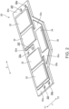
- FIG. 2 is a perspective view of the memory module 26.
- the memory module 26 is, for example, compliant with Compression Attached Memory Module (CAMM).
- the CPU 28a reads and writes data from and to the memory chips 32.
- the present invention is also applicable to modules (such as SSD) other than the memory module 26 and to semiconductor chips (such as CPU) other than the memory chips 32.
- the module board 30 has a front surface 30a on which the memory chips 32 and the power chip 34 are mounted, and a rear surface 30b opposite to the front surface 30a.
- the module board 30 is long in the X direction and short in the Y direction, and has, on one of its long sides, a trapezoidal bulging portion 30c on which the power chip 34 is mounted.
- the X direction, the Y direction, and the below-described Z direction are orthogonal to each other.
- the four memory chips 32 are each approximately square, and are arranged linearly in the X direction.
- the memory chips 32 are adjacent to each other in pairs, and a center screw space 30d is secured between the pairs of memory chips 32. End screw spaces 30e are secured at both ends of the module board 30 in the X direction.
- a stud hole 30f is formed at approximately the center of each of the center screw space 30d and the end screw spaces 30e in the Y direction. The width of each of the center screw space 30d and the end screw spaces 30e in the X direction is about 3 times to 5 times that of the stud hole 30f.
- a stud 44a and a screw 46 (described later) are inserted into the stud hole 30f. In other words, each pair of memory chips 32 are interposed between screws 46 on both sides in the X direction.
- a pin hole 30g is formed in the center screw space 30d on the side (hereafter also referred to as "Y1 side") opposite to the bulging portion 30c and in each end screw space 30e on the side (hereafter also referred to as "Y2 side") near the bulging portion 30c.
- the width of the module board 30 in the Y direction excluding the bulging portion 30c is slightly larger than that of the memory chip 32.
- a large number of contact portions 30h are arranged in a matrix on the rear surface 30b of the module board 30.
- the number of contact portions 30h is 600 or more in this example.
- the contact portions 30h are mostly located on the rear side of the memory chips 32.
- the module board 30 thus has good area efficiency with almost no wasted space on the front surface 30a and the rear surface 30b, which contributes to downsizing of the memory module 26.
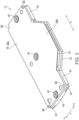
- FIG. 3 is a perspective view of the module mounting structure 12.
- FIG. 4 is an exploded perspective view of the module mounting structure 12.
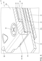
- FIG. 5 is a partially enlarged sectional perspective view of the module mounting structure 12.
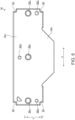
- FIG. 6 is a plan view of a cover 36.
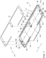
- FIG. 7 is a perspective view of the cover 36 as seen from the rear.
- the module mounting structure 12 includes the cover 36, an insulating sheet (insulating material) 38, thermal interface materials (TIMs) 40, a relay connector board 42, a back plate 44, and three screws (fastening members) 46, in addition to the foregoing memory module 26 and substrate 28.
- the cover 36, the TIMs 40, the memory module 26, the relay connector board 42, the substrate 28, and the back plate 44 that are stacked in this order in the Z direction are fastened by the screws 46.
- the cover 36 covers the front surface 30a of the memory module 26 on which the memory chips 32 are mounted, and is formed by, for example, cutting or die-casting a metal material such as an aluminum material.
- the cover 36 has approximately the same shape and size as the module board 30 in a plan view, and includes a rectangular portion 36a and a trapezoidal bulging portion 36b.
- the bulging portion 36b covers the bulging portion 30c of the module board 30, and the rectangular portion 36a covers the other parts.
- the bulging portion 30c is slightly thinner than the rectangular portion 36a in the Z direction.
- the rectangular portion 36a includes a flat portion 47 and an edge protruding portion 48.
- the edge protruding portion 48 protrudes from the edges of the rectangular portion 36a toward the substrate 28.
- the rectangular portion 36a has high rigidity and is less prone to bending or twisting because the edge protruding portion 48 is formed on its periphery.
- Small module check notches 50 that expose the four corners of the module board 30 are formed at the four corners of the rectangular portion 36a of the cover 36.
- the edge protruding portion 48 has a two-stage shape consisting of a board support protruding portion 48a that abuts on the front surface 30a of the module board 30 along the edges and a wall portion 48b that is outward from the board support protruding portion 48a and protrudes to the edges of the module board 30.
- the board support protruding portion 48a and the wall portion 48b may be separate from each other.
- the board support protruding portion 48a is formed at the edges of both ends of the rectangular portion 36a in the X direction, over the entire length of the edge of the rectangular portion 36a on the Y1 side, and partially on the Y2 side so as to overlap with the bulging portion 36b to some extent.
- the board support protruding portion 48a further includes a portion 36e that protrudes from the edge on the Y1 side toward the Y2 side at an intermediate position in the X direction.
- a screw hole 36c and a pin check hole 36d are provided at each of the portion 36e and the edges of both ends in the X direction.
- the board support protruding portion 48a has an inward route that avoids the module check notches 50 at the four corners of the rectangular portion 36a.
- the board support protruding portion 48a is conceptually shaped as a combination of a square C letter shape and an E letter shape.
- the screw hole 36c and the pin check hole 36d are located at positions corresponding to the stud hole 30
- the wall portion 48b is square C-shaped except for the boundary between the rectangular portion 36a and the bulging portion 36b.
- the wall portion 48b is conceptually shaped as a square C, but is discontinuous at the module check notches 50 at the four corners of the rectangular portion 36a.
- the board support protruding portion 48a abuts on the module board 30 via the insulating sheet 38, along each of the four memory chips 32 and also around (i.e. in a state of surrounding) the four memory chips 32.
- the board support protruding portion 48a is discontinuous at the bulging portion 36b so as not to impose a load on the wiring pattern between the memory chips 32 and the power chip 34.
- the board support protruding portion 48a has an appropriate width so as not to impose a local load on the module board 30.
- the insulating sheet 38 has the same shape as the board support protruding portion 48a, and is attached to the board support protruding portion 48a.
- the insulating sheet 38 has holes and notches corresponding to the stud holes 30f and pin holes 30g.
- the insulating sheet 38 provided between the board support protruding portion 48a and the module board 30 prevents short circuits in the patterns of the module board 30.
- the wall portion 48b protrudes beyond the edges of the module board 30 but does not abut on the substrate 28 (see FIG. 5 ).
- the wall portion 48b abuts on the edges of the module board 30 to position the cover 36.
- the wall portion 48b is thinner than the board support protruding portion 48a. In this example, the wall portion 48b is about 1/5 of the board support protruding portion 48a in thickness.
- the memory chips 32 have little electromagnetic leakage because the cover 36 is located above the memory chips 32, the edge protruding portion 48 covers substantially the entire sides of the memory chips 32, and the back plate 44 is located below the memory chips 32 with the substrate 28 and the like therebetween.
- the TIMs 40 are provided between the cover 36 and the memory chips 32, to transfer heat from the memory chips 32 to the cover 36 and dissipate the heat.
- the TIMs 40 are thermally conductive sheets.
- the area of the cover 36 may be increased or the cover 36 may be in thermal contact with another thermally conductive material.
- the TIMs 40 may be omitted if there is no need to dissipate heat from the memory chips 32.
- FIG. 8 is a schematic sectional view illustrating a screw hole 36c and a screw 46 provided in the screw hole 36c.
- a spot facing 36ca is formed around the screw hole 36c.
- the screw 46 is a captive screw, and has a neck portion 46c between a head portion 46a and a threaded portion 46b. Once the threaded portion 46b has been screwed into and penetrates the female threaded portion of the screw hole 36c, the screw 46 cannot be removed unless it is rotated in the reverse direction. Hence, the screw 46 is basically kept from falling off. It is thus possible to prevent the screw 46 from being lost and from causing a short circuit on the substrate 28, etc.
- the neck portion 46c is provided with a washer 46d.
- the relay connector board 42 is shaped as a rectangle slightly smaller than the rectangular portion 36a of the module board 30.
- the relay connector board 42 is provided between the substrate 28 and the rear side of the parts where the memory chips 42 are mounted and the center screw space 30d of the memory module 26.
- the relay connector board 42 is provided so as to cross the center screw space 30d in this example, the relay connector board 42 may be divided into two parts, one on the left and one on the right, with the center screw space 30d as the boundary.
- the relay connector board 42 has a center screw space 42a and end screw spaces 42b similar to the foregoing center screw space 30d and end screw spaces 30e, and a stud hole 42c is formed in each of the center screw space 42a and the end screw spaces 42b.
- a positioning pin 42d protruding upward and downward is provided in each of the center screw space 42a and the end screw spaces 42b at a position corresponding to the pin hole 30g.
- a large number of elastic pins 42e are provided in the regions other than the center screw space 42a and the end screw spaces 42b.
- the elastic pins 42e are located at positions corresponding to the contact portions 28b of the substrate 28 and the contact portions 30h (see FIGS. 9A and 9B ) of the module board 30.
- the substrate 28 has the contact portions 28b at positions corresponding to the contact portions 30h.
- the substrate 28 has stud holes 28c at positions corresponding to the stud holes 30f, and pin holes 28d at positions corresponding to the pin holes 30g.
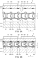
- FIG. 9A is a schematic sectional view illustrating the memory module 26, the relay connector board 42, the substrate 28, and the back plate 44 before assembly.
- FIG. 9B is a schematic sectional view illustrating the memory module 26, the relay connector board 42, the substrate 28, and the back plate 44 after assembly.
- the elastic pins 42e of the relay connector board 42 are roughly heart-shaped and protrude upward and downward before the module mounting structure 12 is assembled. In this stage, the upward and downward protruding parts of each elastic pin 42e are discontinuous and are not in contact with each other at an intermediate position therebetween.
- the relay connector board 42 is sandwiched and pressed by the substrate 28 and the rear surface 30b of the module board 30.
- This causes the elastic pins 42e to be elastically compressed from above and below, as a result of which the contact portions 30h of the module board 30 and the contact portions 28b of the substrate 28 are electrically connected.
- the upward and downward protruding parts of each elastic pin 42e come into contact with each other at the intermediate position, so that electrical resistance between the top and bottom decreases.
- the repulsive force exerted on the contact portions 28b and 30h increases, so that contact resistance decreases.
- the back plate 44 is made of a metal material, and supports the substrate 28 from the rear.
- the back plate 44 is shaped as a rectangle that is approximately the same as the rectangular portion 36a of the module board 30.
- An insulating sheet may be provided between the back plate 44 and the substrate 28.
- the back plate 44 has studs 44a at positions corresponding to the stud holes 30f, and pin holes 44b at positions corresponding to the pin holes 30g.
- each of the three positioning pins 42d of the relay connector board 42 is fitted into the pin hole 30g of the module board 30 for positioning. This part can be checked through the pin check hole 36d of the cover 36.
- the downward protruding part of each of the three positioning pins 42d of the relay connector board 42 is fitted into the respective pin holes 28d and 44b of the substrate 28 and back plate 44 for positioning.
- Each stud 44a is fitted into the respective stud holes 28c, 42c, and 30f of the substrate 28, relay connector board 42, and module board 30 and screwed with the screw 46 provided in the cover 36.
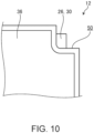
- FIG. 10 is an enlarged plan view illustrating a corner of the cover 36.
- the four corners of the module board 30 can be seen from the module check notches 50 formed at the corners of the cover 36. This makes it possible to check whether the memory module 26 is not missing and is fixed at the correct position.
- FIG. 11 is a schematic sectional view of the module mounting structure 12.
- the edge protruding portion 48 is omitted at the left end so that other parts can be seen, and is not cut at the right end to show the wall portion 48b.
- the board support protruding portion 48a is cut at the boundary with the wall portion 48b, and hatching is omitted to avoid complexity.
- the parts other than the edge protruding portion 48 are cut at the center in the Y direction and hatched.
- the TIMs 40 are omitted.
- the module board 30 is fixed as a result of the three screws 46 being screwed into the studs 44a, and each pair of memory chips 32 are interposed between two screws 46 on both sides and are stable accordingly.
- the contact portions 28b and 30h are subjected to the repulsive force from the elastic pins 42e and, due to the elastic pins 42e being large in number, the force exerted on the module board 30 as a whole from the relay connector board 42 is considerably large, there is a possibility that the intermediate part between the two screws 46 warps as indicated by the imaginary lines to impose stress on the memory chips 32 on the front surface 30a.
- the board support protruding portion 48a of the cover 36 protrudes toward the substrate 28 and abuts on the module board 30 along the memory chips 32.
- the module board 30 can thus be prevented from warping to impose stress on the memory chips 32.
- the board support protruding portion 48a may be flexibly applied depending on the arrangement of the module board 30 and the memory chips 32.
- the four memory chips 32 are arranged linearly in the X direction.
- the board support protruding portion 48a is, at least on the Y1 side (see FIG. 7 ), provided over a range L3 that is longer than the total length L4 of the four memory chips 32 in the X direction, so that the module board 30 can be held flat at least on the Y1 side.
- the range L3 is approximately the entire length of the rectangular portion 36a excluding the module check notches 50. Let L1 be the interval between screws 46. Then, the range L3 includes L1 + L1, which is the range of three screws 46. Thus, the module board 30 can be held flat more reliably.
- the board support protruding portion 48a is preferably located at least at a position including the perpendicular bisector L M of the line segment L1 connecting two screws 46.
- the board support protruding portion 48a is provided at a position including the perpendicular bisector L M on both the Y1 side and the Y2 side of the rectangular portion 36a.
- the board support protruding portion 48a extends not only in the X direction but also in the Y direction, so that the module board 30 can be held flat more reliably.
- the board support protruding portion 48a is provided over the entire length in the Y direction near the memory chips 32 at both ends in the X direction, and these parts of the board support protruding portion 48a and the parts of the board support protruding portion 48a extending in the X direction are integrally connected at their ends.
- the parts extending in the X direction and the parts extending in the Y direction complement each other in strength, with it being possible to hold the module board 30 more reliably.
- Each memory chip 32 is approximately square in most cases.
- the total dimension L4 in the X direction is large whereas the dimension in the Y direction is relatively small. Therefore, even if design constraints or the like make it impossible to provide the board support protruding portion 48a on either the Y1 side or the Y2 side, providing the board support protruding portion 48a along the entire length of the memory chip 32 in the Y direction can prevent warping of the module board 30 appropriately.
- the substrate 28 is also subjected to a large elastic force as with the module board 30, the substrate 28 is supported by the back plate 44 and therefore is prevented from warping. In the case where the substrate 28 has sufficiently high strength, the back plate 44 may be omitted and the studs 44a may be provided directly on the substrate 28.
- the flat portion 47 (see FIG. 7 ) of the cover 36 does not directly contribute to preventing warping of the module board 30 although it has the function of connecting the board support protruding portion 48a on all four sides and the function of preventing electromagnetic leakage and dissipating heat. Therefore, depending on the design conditions, the flat portion 47 does not need to cover the entire rectangular portion 36a and may partially expose the rectangular portion 36a. In the foregoing example, the pin check holes 36d and the module check notches 50 are exposed.
- the flat portion 47 may have holes that allow the model numbers and shapes of the memory chips 32 to be checked.
Landscapes
- Engineering & Computer Science (AREA)
- Theoretical Computer Science (AREA)
- Computer Hardware Design (AREA)
- General Engineering & Computer Science (AREA)
- Human Computer Interaction (AREA)
- Physics & Mathematics (AREA)
- General Physics & Mathematics (AREA)
- Microelectronics & Electronic Packaging (AREA)
- Power Engineering (AREA)
- Mounting Of Printed Circuit Boards And The Like (AREA)
Abstract
Description
- The present invention relates to a module mounting structure in which a module including a module board and chips on the module board is mounted on a substrate, and an electronic apparatus in which a module including a module board and chips on the module board is mounted on a substrate.
- In some electronic apparatuses, a module including a module board and chips on the module board is mounted on a substrate. An example of the module is a memory module. The module is preferably replaceable in order to improve performance or in the event of a failure. In the structure described in the specification of
U.S. Patent Application Publication No. 2023/309227 , a relay connector board including a plurality of elastic pins is provided between a memory module and a substrate, and a large number of contact portions on the rear surface of the memory module and a large number of contact portions on the front surface of the substrate are connected to each other by the elastic pins. In this structure, a large number of contact portions can be provided over a relatively wide area on the rear surface of the module. In this example, the memory module, the relay connector board, and the substrate are stacked and fastened with a plurality of screws and nuts, and the memory module can be removed from the substrate and replaced by removing these screws and nuts. - The memory module in the specification of
U.S. Patent Application Publication No. 2023/309227 has poor area efficiency because the memory chips and the relay connector board differ in attachment position. Area efficiency can be improved if the relay connector board is located on the rear side of the part of the memory module where the memory chips are mounted. However, since the relay connector board has a large number of elastic pins, for example, fastening both ends of the relay connector board with screws may cause the center part to be pushed up by these elastic pins and cause the module board to bend so as to warp. This is likely to impose stress on the chips on the front surface of the module board. - In view of the foregoing problem, the present invention has an object of providing a module mounting structure and electronic apparatus that have good area efficiency and do not impose stress on chips.
- In order to solve the foregoing problem and achieve the stated object, a module mounting structure according to a first aspect of the present invention is a module mounting structure in which a module including a module board and a chip on the module board is mounted on a substrate, the module mounting structure including: a cover that covers a front surface of the module on which the chip is mounted; a relay connector board that is located between a rear side of a part of the module where the chip is mounted and the substrate, and brings a large number of contact portions of the module and a large number of contact portions of the substrate into contact with each other by a large number of elastic pins; and a fastening member that fastens the cover, the module board, the relay connector board, and the substrate that are in a stacked state, in a stacking direction, wherein the cover includes a board support protruding portion that protrudes toward the substrate and abuts on the module board at a position along the chip.
- An electronic apparatus according to a second aspect of the present invention is an electronic apparatus in which a module including a module board and a chip on the module board is mounted on a substrate, the electronic apparatus including: a cover that covers a front surface of the module on which the chip is mounted; a relay connector board that is located between a rear side of a part of the module where the chip is mounted and the substrate, and brings a large number of contact portions of the module and a large number of contact portions of the substrate into contact with each other by a large number of elastic pins; and a fastening member that fastens the cover, the module board, the relay connector board, and the substrate that are in a stacked state, in a stacking direction, wherein the cover includes a board support protruding portion that protrudes toward the substrate and abuts on the module board along a periphery of the chip.
- The above-described aspects of the present invention achieve good area efficiency and do not impose stress on chips.
-
-
FIG. 1 is a perspective view of a laptop PC which is an electronic apparatus according to an embodiment of the present invention. -
FIG. 2 is a perspective view of a memory module. -
FIG. 3 is a perspective view of a module mounting structure. -
FIG. 4 is an exploded perspective view of the module mounting structure. -
FIG. 5 is a partially enlarged sectional perspective view of the module mounting structure. -
FIG. 6 is a plan view of a cover. -
FIG. 7 is a perspective view of the cover as seen from the rear. -
FIG. 8 is a schematic sectional view illustrating a screw hole and a screw provided in the screw hole. -
FIG. 9A is a schematic sectional view illustrating the memory module, relay connector board, substrate, and back plate before assembly. -
FIG. 9B is a schematic sectional view illustrating the memory module, relay connector board, substrate, and back plate after assembly. -
FIG. 10 is an enlarged plan view illustrating a corner of the cover. -
FIG. 11 is a schematic sectional view of the module mounting structure. - Examples of a module mounting structure and electronic apparatus according to an embodiment of the present invention will be described in detail below, with reference to the drawings. The present invention is not limited to such examples.
-
FIG. 1 is a perspective view of alaptop PC 10 which is an electronic apparatus according to an embodiment of the present invention. The laptop PC 10 includes amodule mounting structure 12 according to the embodiment of the present invention. Themodule mounting structure 12 is incorporated inside achassis 14 of the laptop PC 10. The electronic apparatus according to the present invention is not limited to the laptop PC 10, and may be, for example, a desktop PC or a mobile tablet terminal. - The laptop PC 10 includes a
lid 16 that can be opened and closed relative to thechassis 14 byhinges 18. Closing thelid 16 makes the laptop PC 10 compact, which is suitable for mobile use. - The
chassis 14 is provided with akeyboard device 20 and atouch pad 22. The front of thelid 16 is provided with adisplay device 24 which occupies most of its area, and a speaker and a camera (not illustrated). - The
module mounting structure 12 is incorporated inside thechassis 14. Themodule mounting structure 12 includes amemory module 26 and asubstrate 28. Thesubstrate 28 is a main substrate in the laptop PC 10, and is provided inside thechassis 14 approximately across the left and right ends. ACPU 28a that controls the entire laptop PC 10 is mounted on thesubstrate 28. -
FIG. 2 is a perspective view of thememory module 26. In thememory module 26, fourmemory chips 32 and apower chip 34 are mounted on aPCB module board 30. Thememory module 26 is, for example, compliant with Compression Attached Memory Module (CAMM). TheCPU 28a reads and writes data from and to thememory chips 32. The present invention is also applicable to modules (such as SSD) other than thememory module 26 and to semiconductor chips (such as CPU) other than thememory chips 32. - The
module board 30 has afront surface 30a on which thememory chips 32 and thepower chip 34 are mounted, and arear surface 30b opposite to thefront surface 30a. Themodule board 30 is long in the X direction and short in the Y direction, and has, on one of its long sides, a trapezoidal bulgingportion 30c on which thepower chip 34 is mounted. The X direction, the Y direction, and the below-described Z direction are orthogonal to each other. - The four
memory chips 32 are each approximately square, and are arranged linearly in the X direction. Thememory chips 32 are adjacent to each other in pairs, and acenter screw space 30d is secured between the pairs ofmemory chips 32.End screw spaces 30e are secured at both ends of themodule board 30 in the X direction. Astud hole 30f is formed at approximately the center of each of thecenter screw space 30d and theend screw spaces 30e in the Y direction. The width of each of thecenter screw space 30d and theend screw spaces 30e in the X direction is about 3 times to 5 times that of thestud hole 30f. Astud 44a and a screw 46 (described later) are inserted into thestud hole 30f. In other words, each pair ofmemory chips 32 are interposed betweenscrews 46 on both sides in the X direction. - A
pin hole 30g is formed in thecenter screw space 30d on the side (hereafter also referred to as "Y1 side") opposite to the bulgingportion 30c and in eachend screw space 30e on the side (hereafter also referred to as "Y2 side") near the bulgingportion 30c. The width of themodule board 30 in the Y direction excluding the bulgingportion 30c is slightly larger than that of thememory chip 32. A large number ofcontact portions 30h (seeFIG. 9 ) are arranged in a matrix on therear surface 30b of themodule board 30. The number ofcontact portions 30h is 600 or more in this example. Thecontact portions 30h are mostly located on the rear side of thememory chips 32. Themodule board 30 thus has good area efficiency with almost no wasted space on thefront surface 30a and therear surface 30b, which contributes to downsizing of thememory module 26. -
FIG. 3 is a perspective view of themodule mounting structure 12.FIG. 4 is an exploded perspective view of themodule mounting structure 12.FIG. 5 is a partially enlarged sectional perspective view of themodule mounting structure 12.FIG. 6 is a plan view of acover 36.FIG. 7 is a perspective view of thecover 36 as seen from the rear. - The
module mounting structure 12 includes thecover 36, an insulating sheet (insulating material) 38, thermal interface materials (TIMs) 40, arelay connector board 42, aback plate 44, and three screws (fastening members) 46, in addition to the foregoingmemory module 26 andsubstrate 28. In themodule mounting structure 12, thecover 36, theTIMs 40, thememory module 26, therelay connector board 42, thesubstrate 28, and theback plate 44 that are stacked in this order in the Z direction are fastened by thescrews 46. - The
cover 36 covers thefront surface 30a of thememory module 26 on which thememory chips 32 are mounted, and is formed by, for example, cutting or die-casting a metal material such as an aluminum material. - The
cover 36 has approximately the same shape and size as themodule board 30 in a plan view, and includes arectangular portion 36a and a trapezoidal bulgingportion 36b. The bulgingportion 36b covers the bulgingportion 30c of themodule board 30, and therectangular portion 36a covers the other parts. The bulgingportion 30c is slightly thinner than therectangular portion 36a in the Z direction. Therectangular portion 36a includes a flat portion 47 and anedge protruding portion 48. Theedge protruding portion 48 protrudes from the edges of therectangular portion 36a toward thesubstrate 28. Therectangular portion 36a has high rigidity and is less prone to bending or twisting because theedge protruding portion 48 is formed on its periphery. Smallmodule check notches 50 that expose the four corners of themodule board 30 are formed at the four corners of therectangular portion 36a of thecover 36. - The
edge protruding portion 48 has a two-stage shape consisting of a boardsupport protruding portion 48a that abuts on thefront surface 30a of themodule board 30 along the edges and awall portion 48b that is outward from the boardsupport protruding portion 48a and protrudes to the edges of themodule board 30. The boardsupport protruding portion 48a and thewall portion 48b may be separate from each other. - The board
support protruding portion 48a is formed at the edges of both ends of therectangular portion 36a in the X direction, over the entire length of the edge of therectangular portion 36a on the Y1 side, and partially on the Y2 side so as to overlap with the bulgingportion 36b to some extent. The boardsupport protruding portion 48a further includes aportion 36e that protrudes from the edge on the Y1 side toward the Y2 side at an intermediate position in the X direction. Ascrew hole 36c and apin check hole 36d are provided at each of theportion 36e and the edges of both ends in the X direction. The boardsupport protruding portion 48a has an inward route that avoids themodule check notches 50 at the four corners of therectangular portion 36a. The boardsupport protruding portion 48a is conceptually shaped as a combination of a square C letter shape and an E letter shape. Thescrew hole 36c and thepin check hole 36d are located at positions corresponding to thestud hole 30f andpin hole 30g. - The
wall portion 48b is square C-shaped except for the boundary between therectangular portion 36a and the bulgingportion 36b. Thewall portion 48b is conceptually shaped as a square C, but is discontinuous at themodule check notches 50 at the four corners of therectangular portion 36a. - The board
support protruding portion 48a abuts on themodule board 30 via the insulatingsheet 38, along each of the fourmemory chips 32 and also around (i.e. in a state of surrounding) the fourmemory chips 32. The boardsupport protruding portion 48a is discontinuous at the bulgingportion 36b so as not to impose a load on the wiring pattern between thememory chips 32 and thepower chip 34. The boardsupport protruding portion 48a has an appropriate width so as not to impose a local load on themodule board 30. The insulatingsheet 38 has the same shape as the boardsupport protruding portion 48a, and is attached to the boardsupport protruding portion 48a. The insulatingsheet 38 has holes and notches corresponding to the stud holes 30f andpin holes 30g. The insulatingsheet 38 provided between the boardsupport protruding portion 48a and themodule board 30 prevents short circuits in the patterns of themodule board 30. - The
wall portion 48b protrudes beyond the edges of themodule board 30 but does not abut on the substrate 28 (seeFIG. 5 ). Thewall portion 48b abuts on the edges of themodule board 30 to position thecover 36. Thewall portion 48b is thinner than the boardsupport protruding portion 48a. In this example, thewall portion 48b is about 1/5 of the boardsupport protruding portion 48a in thickness. - The
memory chips 32 have little electromagnetic leakage because thecover 36 is located above thememory chips 32, theedge protruding portion 48 covers substantially the entire sides of thememory chips 32, and theback plate 44 is located below thememory chips 32 with thesubstrate 28 and the like therebetween. - The
TIMs 40 are provided between thecover 36 and thememory chips 32, to transfer heat from thememory chips 32 to thecover 36 and dissipate the heat. There are twoTIMs 40 corresponding to the respective pairs ofadjacent memory chips 32. For example, theTIMs 40 are thermally conductive sheets. In order to improve the heat dissipation effect, the area of thecover 36 may be increased or thecover 36 may be in thermal contact with another thermally conductive material. TheTIMs 40 may be omitted if there is no need to dissipate heat from thememory chips 32. -
FIG. 8 is a schematic sectional view illustrating ascrew hole 36c and ascrew 46 provided in thescrew hole 36c. A spot facing 36ca is formed around thescrew hole 36c. Thescrew 46 is a captive screw, and has aneck portion 46c between ahead portion 46a and a threadedportion 46b. Once the threadedportion 46b has been screwed into and penetrates the female threaded portion of thescrew hole 36c, thescrew 46 cannot be removed unless it is rotated in the reverse direction. Hence, thescrew 46 is basically kept from falling off. It is thus possible to prevent thescrew 46 from being lost and from causing a short circuit on thesubstrate 28, etc. Theneck portion 46c is provided with awasher 46d. - Returning to
FIG. 4 , therelay connector board 42 is shaped as a rectangle slightly smaller than therectangular portion 36a of themodule board 30. Therelay connector board 42 is provided between thesubstrate 28 and the rear side of the parts where thememory chips 42 are mounted and thecenter screw space 30d of thememory module 26. Although therelay connector board 42 is provided so as to cross thecenter screw space 30d in this example, therelay connector board 42 may be divided into two parts, one on the left and one on the right, with thecenter screw space 30d as the boundary. Therelay connector board 42 has acenter screw space 42a and endscrew spaces 42b similar to the foregoingcenter screw space 30d andend screw spaces 30e, and astud hole 42c is formed in each of thecenter screw space 42a and theend screw spaces 42b. Moreover, apositioning pin 42d protruding upward and downward is provided in each of thecenter screw space 42a and theend screw spaces 42b at a position corresponding to thepin hole 30g. - In the
relay connector board 42, a large number ofelastic pins 42e are provided in the regions other than thecenter screw space 42a and theend screw spaces 42b. Theelastic pins 42e are located at positions corresponding to thecontact portions 28b of thesubstrate 28 and thecontact portions 30h (seeFIGS. 9A and 9B ) of themodule board 30. - The
substrate 28 has thecontact portions 28b at positions corresponding to thecontact portions 30h. Thesubstrate 28 hasstud holes 28c at positions corresponding to thestud holes 30f, and pinholes 28d at positions corresponding to the pin holes 30g. -
FIG. 9A is a schematic sectional view illustrating thememory module 26, therelay connector board 42, thesubstrate 28, and theback plate 44 before assembly.FIG. 9B is a schematic sectional view illustrating thememory module 26, therelay connector board 42, thesubstrate 28, and theback plate 44 after assembly. - As illustrated in
FIG. 9A , theelastic pins 42e of therelay connector board 42 are roughly heart-shaped and protrude upward and downward before themodule mounting structure 12 is assembled. In this stage, the upward and downward protruding parts of eachelastic pin 42e are discontinuous and are not in contact with each other at an intermediate position therebetween. - As illustrated in
FIG. 9B , after themodule mounting structure 12 is assembled, therelay connector board 42 is sandwiched and pressed by thesubstrate 28 and therear surface 30b of themodule board 30. This causes theelastic pins 42e to be elastically compressed from above and below, as a result of which thecontact portions 30h of themodule board 30 and thecontact portions 28b of thesubstrate 28 are electrically connected. In this stage, the upward and downward protruding parts of eachelastic pin 42e come into contact with each other at the intermediate position, so that electrical resistance between the top and bottom decreases. In addition, the repulsive force exerted on thecontact portions - Returning to
FIG. 4 , theback plate 44 is made of a metal material, and supports thesubstrate 28 from the rear. Theback plate 44 is shaped as a rectangle that is approximately the same as therectangular portion 36a of themodule board 30. An insulating sheet may be provided between theback plate 44 and thesubstrate 28. Theback plate 44 hasstuds 44a at positions corresponding to thestud holes 30f, and pinholes 44b at positions corresponding to the pin holes 30g. - The upward protruding part of each of the three
positioning pins 42d of therelay connector board 42 is fitted into thepin hole 30g of themodule board 30 for positioning. This part can be checked through thepin check hole 36d of thecover 36. The downward protruding part of each of the threepositioning pins 42d of therelay connector board 42 is fitted into therespective pin holes substrate 28 and backplate 44 for positioning. Eachstud 44a is fitted into therespective stud holes substrate 28,relay connector board 42, andmodule board 30 and screwed with thescrew 46 provided in thecover 36. Thus, thecover 36, the insulatingsheet 38, theTMs 40, thememory module 26, therelay connector board 42, thesubstrate 28, and theback plate 44 are fixed in a state of being stacked in the Z direction to form themodule mounting structure 12. -
FIG. 10 is an enlarged plan view illustrating a corner of thecover 36. In the assembledmodule mounting structure 12, the four corners of themodule board 30 can be seen from themodule check notches 50 formed at the corners of thecover 36. This makes it possible to check whether thememory module 26 is not missing and is fixed at the correct position. -
FIG. 11 is a schematic sectional view of themodule mounting structure 12. InFIG. 11 , theedge protruding portion 48 is omitted at the left end so that other parts can be seen, and is not cut at the right end to show thewall portion 48b. The boardsupport protruding portion 48a is cut at the boundary with thewall portion 48b, and hatching is omitted to avoid complexity. The parts other than theedge protruding portion 48 are cut at the center in the Y direction and hatched. TheTIMs 40 are omitted. - As illustrated in
FIG. 11 , themodule board 30 is fixed as a result of the threescrews 46 being screwed into thestuds 44a, and each pair ofmemory chips 32 are interposed between twoscrews 46 on both sides and are stable accordingly. However, since thecontact portions elastic pins 42e and, due to theelastic pins 42e being large in number, the force exerted on themodule board 30 as a whole from therelay connector board 42 is considerably large, there is a possibility that the intermediate part between the twoscrews 46 warps as indicated by the imaginary lines to impose stress on thememory chips 32 on thefront surface 30a. - In view of this, in the
module mounting structure 12 andelectronic apparatus 10 according to this embodiment, the boardsupport protruding portion 48a of thecover 36 protrudes toward thesubstrate 28 and abuts on themodule board 30 along thememory chips 32. Themodule board 30 can thus be prevented from warping to impose stress on thememory chips 32. - The board
support protruding portion 48a may be flexibly applied depending on the arrangement of themodule board 30 and thememory chips 32. In this example, the fourmemory chips 32 are arranged linearly in the X direction. Accordingly, the boardsupport protruding portion 48a is, at least on the Y1 side (seeFIG. 7 ), provided over a range L3 that is longer than the total length L4 of the fourmemory chips 32 in the X direction, so that themodule board 30 can be held flat at least on the Y1 side. The range L3 is approximately the entire length of therectangular portion 36a excluding themodule check notches 50. Let L1 be the interval between screws 46. Then, the range L3 includes L1 + L1, which is the range of threescrews 46. Thus, themodule board 30 can be held flat more reliably. - The
module board 30 is considered to be subjected to the largest force at the midpoint of the line segment L1 connecting twoscrews 46, that is, at the position of the distance L2 (= L1/2) from eachscrew 46. It is therefore preferable that the boardsupport protruding portion 48a holds themodule board 30 at least at this part. In other words, the boardsupport protruding portion 48a is preferably located at least at a position including the perpendicular bisector LM of the line segment L1 connecting twoscrews 46. As illustrated inFIG. 7 , the boardsupport protruding portion 48a is provided at a position including the perpendicular bisector LM on both the Y1 side and the Y2 side of therectangular portion 36a. - The board
support protruding portion 48a extends not only in the X direction but also in the Y direction, so that themodule board 30 can be held flat more reliably. In particular, the boardsupport protruding portion 48a is provided over the entire length in the Y direction near thememory chips 32 at both ends in the X direction, and these parts of the boardsupport protruding portion 48a and the parts of the boardsupport protruding portion 48a extending in the X direction are integrally connected at their ends. Hence, the parts extending in the X direction and the parts extending in the Y direction complement each other in strength, with it being possible to hold themodule board 30 more reliably. - Each
memory chip 32 is approximately square in most cases. When a plurality ofsuch memory chips 32 are arranged linearly in the X direction, the total dimension L4 in the X direction is large whereas the dimension in the Y direction is relatively small. Therefore, even if design constraints or the like make it impossible to provide the boardsupport protruding portion 48a on either the Y1 side or the Y2 side, providing the boardsupport protruding portion 48a along the entire length of thememory chip 32 in the Y direction can prevent warping of themodule board 30 appropriately. Although thesubstrate 28 is also subjected to a large elastic force as with themodule board 30, thesubstrate 28 is supported by theback plate 44 and therefore is prevented from warping. In the case where thesubstrate 28 has sufficiently high strength, theback plate 44 may be omitted and thestuds 44a may be provided directly on thesubstrate 28. - While the board
support protruding portion 48a prevents warping of themodule board 30, the flat portion 47 (seeFIG. 7 ) of thecover 36 does not directly contribute to preventing warping of themodule board 30 although it has the function of connecting the boardsupport protruding portion 48a on all four sides and the function of preventing electromagnetic leakage and dissipating heat. Therefore, depending on the design conditions, the flat portion 47 does not need to cover the entirerectangular portion 36a and may partially expose therectangular portion 36a. In the foregoing example, thepin check holes 36d and themodule check notches 50 are exposed. The flat portion 47 may have holes that allow the model numbers and shapes of thememory chips 32 to be checked. -
- 10
- laptop PC (electronic apparatus)
- 12
- module mounting structure
- 26
- memory module (module)
- 28
- substrate
- 28b, 30h
- contact portion
- 30
- module board
- 30a
- front surface
- 30b
- rear surface
- 30c
- bulging portion
- 32
- memory chip (chip)
- 34
- power chip
- 36
- cover
- 36a
- rectangular portion
- 36b
- bulging portion
- 36c
- screw hole
- 38
- insulating sheet
- 40
- TIM
- 42
- relay connector board
- 42e
- elastic pin
- 44
- back plate
- 44a
- stud
- 46
- screw (fastening member)
- 47
- flat portion
- 48
- edge protruding portion
- 48a
- board support protruding portion
- 48b
- wall portion
- 50
- module check notch
- 1. A module mounting structure in which a module including a module board and a chip on the module board is mounted on a substrate, the module mounting structure comprising:
- a cover that covers a front surface of the module on which the chip is mounted;
- a relay connector board that is located between a rear side of a part of the module where the chip is mounted and the substrate, and brings a large number of contact portions of the module and a large number of contact portions of the substrate into contact with each other by a large number of elastic pins; and
- a fastening member that fastens the cover, the module board, the relay connector board, and the substrate that are in a stacked state, in a stacking direction,
- wherein the cover includes a board support protruding portion that protrudes toward the substrate and abuts on the module board at a position along the chip.
- 2. The module mounting structure according to clause 1, wherein the cover includes a wall portion that is located outward of the board support protruding portion and protrudes to an edge of the module board.
- 3. The module mounting structure according to clause 2, wherein the cover is positioned by the wall portion abutting on the edge of the module board.
- 4. The module mounting structure according to clause 1,
wherein the fastening member comprises a plurality of fastening members, and
wherein the chip is interposed between the plurality of fastening members. - 5. The module mounting structure according to clause 4, wherein the board support protruding portion is provided along an entire length of a line segment connecting two fastening members of the plurality of fastening members.
- 6. The module mounting structure according to clause 4,
wherein the board support protruding portion is provided at least at a position including a perpendicular bisector of a line segment connecting two fastening members of the plurality of fastening members. - 7. The module mounting structure according to clause 1, wherein the chip comprises a plurality of chips that are arranged linearly, and
wherein the board support protruding portion is provided over a total length of the plurality of chips in an arrangement direction, at least on one side of an arrangement of the plurality of chips. - 8. The module mounting structure according to clause 1, wherein the fastening member is a captive screw, and is inserted in a screw hole of the cover so as not to fall off.
- 9. The module mounting structure according to clause 1,
wherein the cover has a module check notch that exposes a corner of the module board. - 10. The module mounting structure according to clause 1, wherein the cover is a metal material.
- 11. The module mounting structure according to
clause 10, comprising a TIM between the cover and the chip. - 12. The module mounting structure according to clause 1, comprising an insulating material between the board support protruding portion and the module board.
- 13. An electronic apparatus in which a module including a module board and a chip on the module board is mounted on a substrate, the electronic apparatus comprising:
- a cover that covers a front surface of the module on which the chip is mounted;
- a relay connector board that is located between a rear side of a part of the module where the chip is mounted and the substrate, and brings a large number of contact portions of the module and a large number of contact portions of the substrate into contact with each other by a large number of elastic pins; and
- a fastening member that fastens the cover, the module board, the relay connector board, and the substrate that are in a stacked state, in a stacking direction,
- wherein the cover includes a board support protruding portion that protrudes toward the substrate and abuts on the module board along a periphery of the chip.
Claims (13)
- A module mounting structure, comprising:a cover arranged to cover a front surface of a module on which at least one chip is mounted;a relay connector board locatable between a rear side of a part of the module where the at least one chip is mounted and a substrate, the relay connector board arranged to bring contact portions of the module and contact portions of the substrate into contact with each other by elastic pins; anda fastening member arranged to fasten together the cover, a module board of the module, the relay connector board, and the substrate in a stacked state,wherein the cover includes a board support protruding portion arranged to protrude toward the substrate and abut the module board at a position along the at least one chip.
- The module mounting structure according to claim 1, wherein the cover includes a wall portion that is located outward of the board support protruding portion and is arranged to protrude to an edge of the module board.
- The module mounting structure according to claim 2, wherein the cover is positionable by the wall portion abutting on the edge of the module board.
- The module mounting structure according to claim 1, wherein the fastening member comprises a plurality of fastening members, and
wherein the at least one chip is interposable between the plurality of fastening members. - The module mounting structure according to claim 4, wherein the board support protruding portion is provided along an entire length of a line segment connecting two fastening members of the plurality of fastening members.
- The module mounting structure according to claim 4, wherein the board support protruding portion is provided at least at a position including a perpendicular bisector of a line segment connecting two fastening members of the plurality of fastening members.
- The module mounting structure according to claim 1, wherein the at least one chip comprises a plurality of chips that are arranged linearly, and
wherein the board support protruding portion is provided over a total length of the plurality of chips in an arrangement direction, at least on one side of an arrangement of the plurality of chips. - The module mounting structure according to claim 1, wherein the fastening member comprises at least one captive screw, at least one captive screw being insertable in a corresponding at least one screw hole of the cover.
- The module mounting structure according to claim 1, wherein the cover comprises a module check notch arranged to expose a corner of the module board.
- The module mounting structure according to claim 1, wherein the cover comprises a metal material.
- The module mounting structure according to claim 10, comprising a thermal interface material, TIM, arrangeable between the cover and the at least one chip.
- The module mounting structure according to claim 1, comprising an insulating material arrangeable between the board support protruding portion and the module board.
- An electronic apparatus comprising a module mounting structure according to any preceding claim.
Applications Claiming Priority (1)
| Application Number | Priority Date | Filing Date | Title |
|---|---|---|---|
| JP2023182638A JP7669444B1 (en) | 2023-10-24 | 2023-10-24 | MODULE MOUNTING STRUCTURE AND ELECTRONIC DEVICE |
Publications (2)
| Publication Number | Publication Date |
|---|---|
| EP4546088A1 true EP4546088A1 (en) | 2025-04-30 |
| EP4546088B1 EP4546088B1 (en) | 2026-05-13 |
Family
ID=92494392
Family Applications (1)
| Application Number | Title | Priority Date | Filing Date |
|---|---|---|---|
| EP24195460.1A Active EP4546088B1 (en) | 2023-10-24 | 2024-08-20 | Module mounting structure and electronic apparatus |
Country Status (4)
| Country | Link |
|---|---|
| US (1) | US20250130611A1 (en) |
| EP (1) | EP4546088B1 (en) |
| JP (1) | JP7669444B1 (en) |
| CN (1) | CN119893837A (en) |
Citations (3)
| Publication number | Priority date | Publication date | Assignee | Title |
|---|---|---|---|---|
| US20220272880A1 (en) * | 2022-05-10 | 2022-08-25 | Intel Corporation | High speed grid array module |
| US20230014167A1 (en) * | 2021-07-15 | 2023-01-19 | Dell Products, L.P. | Thermal heatsink systems and methods in information handling systems |
| US20230309227A1 (en) | 2022-03-28 | 2023-09-28 | Dell Products L.P. | Compression attached memory module (camm) for low-power double data rage (lpddr) memories |
Family Cites Families (5)
| Publication number | Priority date | Publication date | Assignee | Title |
|---|---|---|---|---|
| JP2582259Y2 (en) * | 1992-09-22 | 1998-09-30 | 日本航空電子工業株式会社 | Wire bond contacts |
| US7819693B2 (en) | 2008-09-30 | 2010-10-26 | Hon Hai Precision Ind. Co., Ltd. | LGA socket having improved standoff |
| US11621212B2 (en) | 2019-12-19 | 2023-04-04 | International Business Machines Corporation | Backing plate with manufactured features on top surface |
| US12588149B2 (en) | 2022-06-03 | 2026-03-24 | Intel Corporation | GDDR memory expander using CMT connector |
| US20230005882A1 (en) | 2022-09-02 | 2023-01-05 | Intel Corporation | Memory on package (mop) with reverse camm (compression attached memory module) and cmt connector |
-
2023
- 2023-10-24 JP JP2023182638A patent/JP7669444B1/en active Active
-
2024
- 2024-08-20 EP EP24195460.1A patent/EP4546088B1/en active Active
- 2024-08-30 US US18/820,935 patent/US20250130611A1/en active Pending
- 2024-10-21 CN CN202411467463.9A patent/CN119893837A/en active Pending
Patent Citations (3)
| Publication number | Priority date | Publication date | Assignee | Title |
|---|---|---|---|---|
| US20230014167A1 (en) * | 2021-07-15 | 2023-01-19 | Dell Products, L.P. | Thermal heatsink systems and methods in information handling systems |
| US20230309227A1 (en) | 2022-03-28 | 2023-09-28 | Dell Products L.P. | Compression attached memory module (camm) for low-power double data rage (lpddr) memories |
| US20220272880A1 (en) * | 2022-05-10 | 2022-08-25 | Intel Corporation | High speed grid array module |
Also Published As
| Publication number | Publication date |
|---|---|
| JP2025072109A (en) | 2025-05-09 |
| US20250130611A1 (en) | 2025-04-24 |
| EP4546088B1 (en) | 2026-05-13 |
| JP7669444B1 (en) | 2025-04-28 |
| CN119893837A (en) | 2025-04-25 |
Similar Documents
| Publication | Publication Date | Title |
|---|---|---|
| US5933343A (en) | Multi-deck power converter module | |
| US7679913B2 (en) | Memory module assembly and heat sink thereof | |
| US5673176A (en) | Integrated circuit dual cooling paths and method for constructing same | |
| CN101005054A (en) | memory module cooler | |
| US5990549A (en) | Thermal bus bar design for an electronic cartridge | |
| US6071149A (en) | Electrical card connector | |
| US7161238B2 (en) | Structural reinforcement for electronic substrate | |
| US20110051363A1 (en) | Computer enclosure and data storage device bracket of the computer enclosure | |
| CN102842545B (en) | Heat dissipation component and its combined structure with chipset | |
| US4764122A (en) | Data bus connector | |
| US20120099269A1 (en) | Motherboard and electronic device employing the same | |
| US10123441B2 (en) | Memory device with daughter board fastening structure | |
| CN110657112B (en) | Fan module and electronic device with same | |
| JP7531669B1 (en) | Heat dissipation structure and electronic device | |
| KR20060016236A (en) | Expansion Board Structure Inserted Into Desktop Personal Computer | |
| EP4546088B1 (en) | Module mounting structure and electronic apparatus | |
| JP2001119107A (en) | Printed wiring board | |
| US7330353B2 (en) | Modular heat sink fin modules for CPU | |
| JP7115032B2 (en) | substrate | |
| US20230009649A1 (en) | Circuit board module | |
| CN112698705B (en) | Heat dissipation mechanism and expansion card module using the heat dissipation mechanism | |
| JPH09199665A (en) | Mounting device | |
| KR20030078301A (en) | Memory module and computer device having the same | |
| CN202111283U (en) | Electrical connector assembly and its heat dissipation assembly | |
| CN220122256U (en) | Wireless module protective cover |
Legal Events
| Date | Code | Title | Description |
|---|---|---|---|
| PUAI | Public reference made under article 153(3) epc to a published international application that has entered the european phase |
Free format text: ORIGINAL CODE: 0009012 |
|
| STAA | Information on the status of an ep patent application or granted ep patent |
Free format text: STATUS: THE APPLICATION HAS BEEN PUBLISHED |
|
| AK | Designated contracting states |
Kind code of ref document: A1 Designated state(s): AL AT BE BG CH CY CZ DE DK EE ES FI FR GB GR HR HU IE IS IT LI LT LU LV MC ME MK MT NL NO PL PT RO RS SE SI SK SM TR |
|
| STAA | Information on the status of an ep patent application or granted ep patent |
Free format text: STATUS: REQUEST FOR EXAMINATION WAS MADE |
|
| 17P | Request for examination filed |
Effective date: 20250609 |
|
| REG | Reference to a national code |
Ref country code: DE Ref legal event code: R079 Free format text: PREVIOUS MAIN CLASS: G06F0001180000 Ipc: G06F0001160000 Ref country code: DE Ref legal event code: R079 Ref document number: 602024004694 Country of ref document: DE Free format text: PREVIOUS MAIN CLASS: G06F0001180000 Ipc: G06F0001160000 |
|
| RIC1 | Information provided on ipc code assigned before grant |
Ipc: G06F 1/16 20060101AFI20251021BHEP Ipc: G06F 1/18 20060101ALI20251021BHEP |
|
| GRAP | Despatch of communication of intention to grant a patent |
Free format text: ORIGINAL CODE: EPIDOSNIGR1 |
|
| STAA | Information on the status of an ep patent application or granted ep patent |
Free format text: STATUS: GRANT OF PATENT IS INTENDED |
|
| INTG | Intention to grant announced |
Effective date: 20251127 |
|
| GRAS | Grant fee paid |
Free format text: ORIGINAL CODE: EPIDOSNIGR3 |
|
| GRAA | (expected) grant |
Free format text: ORIGINAL CODE: 0009210 |
|
| STAA | Information on the status of an ep patent application or granted ep patent |
Free format text: STATUS: THE PATENT HAS BEEN GRANTED |
|
| AK | Designated contracting states |
Kind code of ref document: B1 Designated state(s): AL AT BE BG CH CY CZ DE DK EE ES FI FR GB GR HR HU IE IS IT LI LT LU LV MC ME MK MT NL NO PL PT RO RS SE SI SK SM TR |
|
| REG | Reference to a national code |
Ref country code: CH Ref legal event code: F10 Free format text: ST27 STATUS EVENT CODE: U-0-0-F10-F00 (AS PROVIDED BY THE NATIONAL OFFICE) Effective date: 20260513 |