EP4546038A1 - Liquid crystal display - Google Patents
Liquid crystal display Download PDFInfo
- Publication number
- EP4546038A1 EP4546038A1 EP24207462.3A EP24207462A EP4546038A1 EP 4546038 A1 EP4546038 A1 EP 4546038A1 EP 24207462 A EP24207462 A EP 24207462A EP 4546038 A1 EP4546038 A1 EP 4546038A1
- Authority
- EP
- European Patent Office
- Prior art keywords
- liquid crystal
- reflectance
- reflection layer
- interface
- generated
- Prior art date
- Legal status (The legal status is an assumption and is not a legal conclusion. Google has not performed a legal analysis and makes no representation as to the accuracy of the status listed.)
- Pending
Links
Images


Classifications
-
- G—PHYSICS
- G02—OPTICS
- G02F—OPTICAL DEVICES OR ARRANGEMENTS FOR THE CONTROL OF LIGHT BY MODIFICATION OF THE OPTICAL PROPERTIES OF THE MEDIA OF THE ELEMENTS INVOLVED THEREIN; NON-LINEAR OPTICS; FREQUENCY-CHANGING OF LIGHT; OPTICAL LOGIC ELEMENTS; OPTICAL ANALOGUE/DIGITAL CONVERTERS
- G02F1/00—Devices or arrangements for the control of the intensity, colour, phase, polarisation or direction of light arriving from an independent light source, e.g. switching, gating or modulating; Non-linear optics
- G02F1/01—Devices or arrangements for the control of the intensity, colour, phase, polarisation or direction of light arriving from an independent light source, e.g. switching, gating or modulating; Non-linear optics for the control of the intensity, phase, polarisation or colour
- G02F1/13—Devices or arrangements for the control of the intensity, colour, phase, polarisation or direction of light arriving from an independent light source, e.g. switching, gating or modulating; Non-linear optics for the control of the intensity, phase, polarisation or colour based on liquid crystals, e.g. single liquid crystal display cells
- G02F1/133—Constructional arrangements; Operation of liquid crystal cells; Circuit arrangements
- G02F1/1333—Constructional arrangements; Manufacturing methods
- G02F1/1335—Structural association of cells with optical devices, e.g. polarisers or reflectors
- G02F1/133502—Antiglare, refractive index matching layers
-
- G—PHYSICS
- G02—OPTICS
- G02F—OPTICAL DEVICES OR ARRANGEMENTS FOR THE CONTROL OF LIGHT BY MODIFICATION OF THE OPTICAL PROPERTIES OF THE MEDIA OF THE ELEMENTS INVOLVED THEREIN; NON-LINEAR OPTICS; FREQUENCY-CHANGING OF LIGHT; OPTICAL LOGIC ELEMENTS; OPTICAL ANALOGUE/DIGITAL CONVERTERS
- G02F1/00—Devices or arrangements for the control of the intensity, colour, phase, polarisation or direction of light arriving from an independent light source, e.g. switching, gating or modulating; Non-linear optics
- G02F1/01—Devices or arrangements for the control of the intensity, colour, phase, polarisation or direction of light arriving from an independent light source, e.g. switching, gating or modulating; Non-linear optics for the control of the intensity, phase, polarisation or colour
- G02F1/13—Devices or arrangements for the control of the intensity, colour, phase, polarisation or direction of light arriving from an independent light source, e.g. switching, gating or modulating; Non-linear optics for the control of the intensity, phase, polarisation or colour based on liquid crystals, e.g. single liquid crystal display cells
- G02F1/133—Constructional arrangements; Operation of liquid crystal cells; Circuit arrangements
- G02F1/1333—Constructional arrangements; Manufacturing methods
- G02F1/133308—Support structures for LCD panels, e.g. frames or bezels
- G02F1/133331—Cover glasses
-
- G—PHYSICS
- G02—OPTICS
- G02B—OPTICAL ELEMENTS, SYSTEMS OR APPARATUS
- G02B1/00—Optical elements characterised by the material of which they are made; Optical coatings for optical elements
- G02B1/10—Optical coatings produced by application to, or surface treatment of, optical elements
- G02B1/11—Anti-reflection coatings
-
- G—PHYSICS
- G02—OPTICS
- G02F—OPTICAL DEVICES OR ARRANGEMENTS FOR THE CONTROL OF LIGHT BY MODIFICATION OF THE OPTICAL PROPERTIES OF THE MEDIA OF THE ELEMENTS INVOLVED THEREIN; NON-LINEAR OPTICS; FREQUENCY-CHANGING OF LIGHT; OPTICAL LOGIC ELEMENTS; OPTICAL ANALOGUE/DIGITAL CONVERTERS
- G02F1/00—Devices or arrangements for the control of the intensity, colour, phase, polarisation or direction of light arriving from an independent light source, e.g. switching, gating or modulating; Non-linear optics
- G02F1/01—Devices or arrangements for the control of the intensity, colour, phase, polarisation or direction of light arriving from an independent light source, e.g. switching, gating or modulating; Non-linear optics for the control of the intensity, phase, polarisation or colour
- G02F1/13—Devices or arrangements for the control of the intensity, colour, phase, polarisation or direction of light arriving from an independent light source, e.g. switching, gating or modulating; Non-linear optics for the control of the intensity, phase, polarisation or colour based on liquid crystals, e.g. single liquid crystal display cells
- G02F1/133—Constructional arrangements; Operation of liquid crystal cells; Circuit arrangements
- G02F1/1333—Constructional arrangements; Manufacturing methods
- G02F1/1335—Structural association of cells with optical devices, e.g. polarisers or reflectors
- G02F1/133509—Filters, e.g. light shielding masks
- G02F1/133512—Light shielding layers, e.g. black matrix
-
- G—PHYSICS
- G02—OPTICS
- G02F—OPTICAL DEVICES OR ARRANGEMENTS FOR THE CONTROL OF LIGHT BY MODIFICATION OF THE OPTICAL PROPERTIES OF THE MEDIA OF THE ELEMENTS INVOLVED THEREIN; NON-LINEAR OPTICS; FREQUENCY-CHANGING OF LIGHT; OPTICAL LOGIC ELEMENTS; OPTICAL ANALOGUE/DIGITAL CONVERTERS
- G02F2201/00—Constructional arrangements not provided for in groups G02F1/00 - G02F7/00
- G02F2201/38—Anti-reflection arrangements
-
- G—PHYSICS
- G02—OPTICS
- G02F—OPTICAL DEVICES OR ARRANGEMENTS FOR THE CONTROL OF LIGHT BY MODIFICATION OF THE OPTICAL PROPERTIES OF THE MEDIA OF THE ELEMENTS INVOLVED THEREIN; NON-LINEAR OPTICS; FREQUENCY-CHANGING OF LIGHT; OPTICAL LOGIC ELEMENTS; OPTICAL ANALOGUE/DIGITAL CONVERTERS
- G02F2202/00—Materials and properties
- G02F2202/28—Adhesive materials or arrangements
Definitions
- the present disclosure relates to a liquid crystal display, and more particularly to a seamless boundary between a display region for displaying an image and a light-shielding region.
- the liquid crystal display includes a liquid crystal module housed in a housing, and the liquid crystal module includes a liquid crystal panel and a protective cover mounted on a front surface of the liquid crystal panel.
- the liquid crystal display includes a display region (active area) for displaying an image and a light-shielding region surrounding the display region, and what is known as a black mask for defining the light-shielding region is formed on an outer periphery of the protective cover.
- the black mask is, for example, a region in which black color is printed on the protective cover.
- the black mask is prevented from being conspicuous by providing an intermediate layer such as a checkered pattern on the black mask.
- a liquid crystal display according to an aspect of the present disclosure includes: a liquid crystal module; a cover glass provided on the liquid crystal module; a light-shielding region formed on an outer periphery of a back surface side of the cover glass; and an anti-reflection layer formed on a front surface side of the cover glass.
- the anti-reflection layer includes a first anti-reflection layer corresponding to a display region for displaying an image and a second anti-reflection layer corresponding to the light-shielding region, and a reflectance generated at a front surface of the second anti-reflection layer is greater than that generated on a front surface of the first anti-reflection layer.
- reflectances of the first and second anti-reflection layers are determined such that a sum of the reflectance generated at the interface of the light-shielding region and the reflectance generated at the front surface of the second anti-reflection layer is approximately equal to a sum of the reflectance generated at the interface of each layer in the liquid crystal module of the display region and the reflectance generated at the front surface of the first anti-reflection layer.
- the reflectance generated at the interface of each layer in the liquid crystal module includes the reflectance generated at the interface of a shield electrode and a glass substrate, the reflectance generated at the interface of the glass substrate and the liquid crystal panel, and the reflectance generated at the interface of the liquid crystal panel and a TFT substrate.
- a liquid crystal display includes a liquid crystal module, a cover glass provided on the liquid crystal module, a light shielding region formed on an outer periphery of a back surface side of the cover glass, an adhesive portion formed on a front surface side of the cover glass, and an anti-reflection layer formed on the adhesive portion.
- the adhesive portion includes a first adhesive portion corresponding to a display region for displaying an image and a second adhesive portion corresponding to the light shielding region, and a reflectance generated at an interface between the second adhesive portion and the anti-reflection layer is greater than the reflectance generated at the interface between the first adhesive portion and the anti-reflection layer.
- the reflectances of the first and second adhesive portions are determined such that a sum of the reflectance generated at the interface of the light shielding region, the reflectance generated at the interface of the second adhesive portion, and the reflectance generated at the front surface of the anti-reflection layer is approximately equal to a sum of the reflectance generated at the interface of each layer in the liquid crystal module of the display region, the reflectance generated at the interface of the first adhesive portion, and the reflectance generated at the front surface of the anti-reflection layer.
- the reflectance generated at the interface of each layer in the liquid crystal module includes the reflectance generated at the interface between the glass substrate and the liquid crystal panel, and the reflectance generated at the interface between the liquid crystal panel and the TFT substrate.
- the shield electrode is formed of an organic conductive film, and the reflectance generated at the interface between the shield electrode and the glass substrate is suppressed.
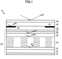
- FIG. 1 is a diagram illustrating a schematic cross section of an existing liquid crystal display.
- a liquid crystal display 10 includes a liquid crystal module 20, a cover glass 40 provided on the liquid crystal module 20 via an optical clear film (optically clear resin (OCR)) or an optical clear adhesive (optically clear adhesive (OCA)) 30, and an anti-reflection (AR) layer or an anti-static film (ASF) 50 formed on a front surface of the cover glass 40.
- OCR optical clear resin
- OCA optical clear adhesive
- AR anti-reflection
- ASF anti-static film
- the liquid crystal module 20 is formed by laminating, in the order from the bottom, a polarizing plate 21, a glass substrate 22, an array (AR) substrate with a thin film transistor (TFT) 23 (hereinafter, also referred to as TFT substrate) formed on the glass substrate 22, a liquid crystal panel 24 including an RGB filter and liquid crystal molecules, a glass substrate 25, a shield electrode 26, and a polarizing plate 27.
- a backlight (illustration omitted) is arranged below the liquid crystal module 20.
- the liquid crystal panel 24 is, for example, of an IPS type in which the liquid crystal molecules rotate in a horizontal direction relative to the liquid crystal panel by a voltage applied via the TFT.
- the shield electrode 26 for discharging an electric charge charged above the liquid crystal panel 24 to a GND (reference potential) is arranged between the glass substrate 25 and the polarizing plate 27.
- the shield electrode 26 is made of, for example, a light-transmitting transparent metal material such as indium tin oxide (ITO).
- a liquid crystal display in which a boundary between a display region for displaying an image and a light-shielding region is made seamless is provided.
- Embodiments of the present disclosure will now be described.
- the present disclosure is particularly applied to a liquid crystal display including a touch panel function as a user interface and a liquid crystal display including a function for detecting proximity of a user's finger or the like using infrared rays or the like, in addition to a liquid crystal display having a general image display function.
- FIG. 2A is a diagram illustrating a schematic plan view of a liquid crystal display according to a first embodiment of the present disclosure.
- FIG. 2B is a diagram illustrating a schematic cross-sectional view taken along the line A-A.
- a liquid crystal display 100 according to the present embodiment is formed by housing a backlight and a liquid crystal module 20 in a substantially rectangular housing. As illustrated in FIG. 2A , when viewed from above, the liquid crystal display 100 includes a rectangular active area (display region) P for displaying an image, and a light-shielding area Q surrounding an outer periphery of the active area P.
- the light-shielding area Q is a non-display region in which no image is displayed.
- the cover glass (protective glass) 40 is mounted on the polarizing plate 27 of the liquid crystal module 20 via the optical clear film (OCR) or the optical clear adhesive (OCA) 30.
- the black mask 42 defining the light-shielding area Q is formed on the back side of the cover glass 40 by screen printing or the like.
- the cover glass 40 normally has a reflectance of 3% to 4%, but the reflectance of the cover glass 40 is reduced by forming the anti-reflection layer 110.
- the first anti-reflection layer 110A is, although materials or thickness thereof is not particularly limited, formed of a single layer film or a multilayer film, and in a case of the multilayer film, a high reflectance can be reduced by alternately laminating, for example, a low refractive material (e.g., MgF 2 , SiO 2 , Al 2 O 3 , etc.) and a high refractive material (e.g., ZrO 2 , CeO 2 , ZnS, etc.).
- a low refractive material e.g., MgF 2 , SiO 2 , Al 2 O 3 , etc.
- a high refractive material e.g., ZrO 2 , CeO 2 , ZnS, etc.
- the first anti-reflection layer 110A is formed, for example, by depositing, sputtering, and applying a material to the front surface of the cover glass 40.
- the reflectance of the front surface of the first anti-reflection layer 110A is R1 ⁇ 0.3%, consistent with the anti-reflection layer of the liquid crystal display 10 as illustrated in FIG. 1 .
- the second anti-reflection layer 110B is formed of, for example, a resin or paint of hollow nanosilica, although materials or film thickness of the second anti-reflection layer 110B is not particularly limited.
- the reflectance R BM of the second anti-reflection layer 110B is R BM ⁇ 1.2% when the reflectance R1 of the first anti-reflection layer 110A is ⁇ 0.3%.
- FIGS. 3A, 3B, 3C, and 3D are diagrams illustrating one example of a method of manufacturing the first anti-reflection layer 110A and the second anti-reflection layer 110B.
- a mask member 120 patterned so as to expose the active area P is formed on the cover glass 40, and then, as illustrated in FIG. 3B , a material for forming the first anti-reflection layer 110A is deposited on the area exposed by the mask member 120.
- FIG. 3C after the mask member 120 is removed, as illustrated in FIG. 3D , a material for forming the second anti-reflection layer 110B is applied to an area surrounding the first anti-reflection layer 110A.
- the anti-reflection layer 110 having the first anti-reflection layer 110A corresponding to the active area P and the second anti-reflection layer 110B corresponding to the light-shielding area Q, which are two anti-reflection layers having different reflectances, is formed on the cover glass 40.
- the reflectance when viewed from above is determined by the reflectance of the front surface and the reflectance of the interface.
- the boundary B between the active area P and the light-shielding area Q is made inconspicuous, and the boundary B can be made seamless.
- the first anti-reflection layer 110A and the second anti-reflection layer 110B having different refractive indices are formed on the cover glass 40.
- adhesives having different refractive indices are formed on the cover glass 40, and the anti-reflection layer is formed on the adhesives.
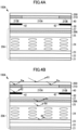
- FIGS. 4A and 4B are diagrams illustrating cross-sectional views of a schematic configuration of a liquid crystal display according to the second embodiment, and the same reference numerals are given to the same components as those illustrated in FIG. 2B .
- a film, anti-reflection film 200 is adhered to the front surface of the cover glass 40 via an adhesive 210.
- the adhesive 210 includes a first adhesive portion 210A having a shape corresponding to the active area P and a second adhesive portion 210B having a shape corresponding to the light-shielding area Q or the black mask 42.
- the second adhesive portion 210B is configured to have a greater reflectance at the interface than the first adhesive portion 210A.
- FIG. 4B is a diagram illustrating reflectances in addition to FIG.
- a shield electrode 26A of a liquid crystal module 20A is formed of an organic conductive film such as a conductive plastic.
- a metal material such as ITO
- the reflectance R3 at the interface with the glass substrate 25 is high (in the example of FIG. 2B , R3 ⁇ 0.7%).
- the refractive index is smaller than that of the metal material, and the reflectance R3 at the interface with the glass substrate 25 can be made to be almost zero or mostly suppressed.
- the shield electrode 26A is made of an organic conductive material, the reflectance R3 ⁇ 0%.
- the reflectance R A of the active area and the reflectance R B of the black mask area can be made approximately the same level.
- the boundary B can be made inconspicuous and thus seamless.
- the liquid crystal module includes an IPS type liquid crystal panel
- the liquid crystal module is not limited thereto, and a VA type or TN type liquid crystal panel may be used.
- the first embodiment and the second embodiment have been described separately, the present disclosure may include a combination of the first embodiment and the second embodiment.
- the reflectance generated at the front surface of the second anti-reflection layer corresponding to the light-shielding region greater than the reflectance generated at the front surface of the first anti-reflection layer corresponding to the display region, a reflectance difference between the light-shielding region and the display region is reduced, and a boundary between the light-shielding region and the display region can be made inconspicuous and thus seamless.
- the reflectance generated at the interface of the second adhesive portion corresponding to the light-shielding region greater than the reflectance generated at the interface of the first adhesive portion corresponding to the display region, the reflectance difference between the light-shielding region and the display region is reduced, and the boundary between the light-shielding region and the display region can be made inconspicuous and thus seamless.
Landscapes
- Physics & Mathematics (AREA)
- Nonlinear Science (AREA)
- General Physics & Mathematics (AREA)
- Optics & Photonics (AREA)
- Mathematical Physics (AREA)
- Chemical & Material Sciences (AREA)
- Crystallography & Structural Chemistry (AREA)
- Liquid Crystal (AREA)
Abstract
Description
- The present disclosure relates to a liquid crystal display, and more particularly to a seamless boundary between a display region for displaying an image and a light-shielding region.
- The liquid crystal display includes a liquid crystal module housed in a housing, and the liquid crystal module includes a liquid crystal panel and a protective cover mounted on a front surface of the liquid crystal panel. The liquid crystal display includes a display region (active area) for displaying an image and a light-shielding region surrounding the display region, and what is known as a black mask for defining the light-shielding region is formed on an outer periphery of the protective cover. The black mask is, for example, a region in which black color is printed on the protective cover. For example, in the liquid crystal display disclosed in
JP 2019-15772A - The present disclosure relates to a liquid crystal display according to the appended claims. Embodiments are disclosed in the dependent claims. A liquid crystal display according to an aspect of the present disclosure includes: a liquid crystal module; a cover glass provided on the liquid crystal module; a light-shielding region formed on an outer periphery of a back surface side of the cover glass; and an anti-reflection layer formed on a front surface side of the cover glass. The anti-reflection layer includes a first anti-reflection layer corresponding to a display region for displaying an image and a second anti-reflection layer corresponding to the light-shielding region, and a reflectance generated at a front surface of the second anti-reflection layer is greater than that generated on a front surface of the first anti-reflection layer.
- In one embodiment, reflectances of the first and second anti-reflection layers are determined such that a sum of the reflectance generated at the interface of the light-shielding region and the reflectance generated at the front surface of the second anti-reflection layer is approximately equal to a sum of the reflectance generated at the interface of each layer in the liquid crystal module of the display region and the reflectance generated at the front surface of the first anti-reflection layer. In one embodiment, the reflectance generated at the interface of each layer in the liquid crystal module includes the reflectance generated at the interface of a shield electrode and a glass substrate, the reflectance generated at the interface of the glass substrate and the liquid crystal panel, and the reflectance generated at the interface of the liquid crystal panel and a TFT substrate.
- A liquid crystal display according to a further aspect of the present disclosure includes a liquid crystal module, a cover glass provided on the liquid crystal module, a light shielding region formed on an outer periphery of a back surface side of the cover glass, an adhesive portion formed on a front surface side of the cover glass, and an anti-reflection layer formed on the adhesive portion. The adhesive portion includes a first adhesive portion corresponding to a display region for displaying an image and a second adhesive portion corresponding to the light shielding region, and a reflectance generated at an interface between the second adhesive portion and the anti-reflection layer is greater than the reflectance generated at the interface between the first adhesive portion and the anti-reflection layer.
- In one embodiment, the reflectances of the first and second adhesive portions are determined such that a sum of the reflectance generated at the interface of the light shielding region, the reflectance generated at the interface of the second adhesive portion, and the reflectance generated at the front surface of the anti-reflection layer is approximately equal to a sum of the reflectance generated at the interface of each layer in the liquid crystal module of the display region, the reflectance generated at the interface of the first adhesive portion, and the reflectance generated at the front surface of the anti-reflection layer. In one embodiment, the reflectance generated at the interface of each layer in the liquid crystal module includes the reflectance generated at the interface between the glass substrate and the liquid crystal panel, and the reflectance generated at the interface between the liquid crystal panel and the TFT substrate. In one embodiment, the shield electrode is formed of an organic conductive film, and the reflectance generated at the interface between the shield electrode and the glass substrate is suppressed.
-
FIG. 1 is a diagram illustrating a cross-sectional view of a schematic configuration of an existing liquid crystal display; -
FIG. 2A is diagram illustrating a schematic plan view of a liquid crystal display according to a first embodiment of the present disclosure; -
FIG. 2B is a diagram illustrating a schematic cross-sectional view taken along a line A-A; -
FIGS. 3A, 3B, 3C, and 3D are diagrams illustrating cross-sectional views of one example of a method of manufacturing an anti-reflection layer according to the first embodiment; and -
FIGS. 4A and 4B are diagrams illustrating schematic cross-sectional views of a liquid crystal display according to a second embodiment of the present disclosure. -
FIG. 1 is a diagram illustrating a schematic cross section of an existing liquid crystal display. Aliquid crystal display 10 includes aliquid crystal module 20, acover glass 40 provided on theliquid crystal module 20 via an optical clear film (optically clear resin (OCR)) or an optical clear adhesive (optically clear adhesive (OCA)) 30, and an anti-reflection (AR) layer or an anti-static film (ASF) 50 formed on a front surface of thecover glass 40. - The
liquid crystal module 20 is formed by laminating, in the order from the bottom, a polarizingplate 21, aglass substrate 22, an array (AR) substrate with a thin film transistor (TFT) 23 (hereinafter, also referred to as TFT substrate) formed on theglass substrate 22, aliquid crystal panel 24 including an RGB filter and liquid crystal molecules, aglass substrate 25, ashield electrode 26, and a polarizingplate 27. A backlight (illustration omitted) is arranged below theliquid crystal module 20. - The
liquid crystal panel 24 is, for example, of an IPS type in which the liquid crystal molecules rotate in a horizontal direction relative to the liquid crystal panel by a voltage applied via the TFT. Normally, in the IPS type, theshield electrode 26 for discharging an electric charge charged above theliquid crystal panel 24 to a GND (reference potential) is arranged between theglass substrate 25 and the polarizingplate 27. Theshield electrode 26 is made of, for example, a light-transmitting transparent metal material such as indium tin oxide (ITO). - A
black mask 42 is formed on an outer periphery of thecover glass 40 so as to surround an active area for displaying an image. Theblack mask 42 is formed, for example, by screen printing a black pigment on a bottom surface of thecover glass 40, and theblack mask 42 defines a light-shielding region. - In the
liquid crystal display 10, the following reflections are generated by light from above (that is, when the liquid crystal display is viewed from above), a reflectance of the front surface, and the reflectance of an interface of each layer. - R1: reflection at the front surface of the anti-reflection film/
anti-static film 50; reflectance = about 0.3%, - R2: reflection at the interface of the
black mask 42; reflectance = about 0.2%, - R3: reflection at the interface of the
shield electrode 26 and theglass substrate 25; reflectance = about 0.7%, - R4: reflection at the interface of the
glass substrate 25 and theliquid crystal panel 24; reflectance = about 0.2%, and - R5: reflection at the interface of the
liquid crystal panel 24 and aTFT substrate 23; reflectance = about 0.2%. - Since refractive indices of the polarizing plate, the OCA, and the glass are approximately 1.5, reflection at the interface due to a refractive index difference hardly occurs.
- A reflectance RA of the active area is RA = R1 + R3 + R4 + R5 ≈ 1.4%, and a reflectance RB of a black mask area is RB = R1 + R2 ≈ 0.5%.
- Accordingly, there is an issue that the reflectance RA of the active area is higher than the reflectance RB of the black mask area and thus their boundary being conspicuous. Conventionally, in order to make this boundary less visible, a method has been employed in which the reflectance RB of the black mask area is increased, the reflectance RA of the active area is decreased, or the reflectances of both are changed.
- In an existing method, the pigment is adjusted in order to increase the reflectance RB of the black mask area, but there is a limit to the pigment adjustment for reasons such as reliability and material restriction due to color, and the reflectance cannot be increased very much. On the other hand, in order to decrease the reflectance RA of the active area, it is also possible to change the metal material (for example, ITO) of the
shield electrode 26 to an organic conductive material (for example, conductive plastics, etc.), but in doing so, a resistance value of theshield electrode 26 becomes high, and discharge of the electric charge by electrical static discharge (ESD) may become insufficient. - According to an aspect of the present disclosure, a liquid crystal display in which a boundary between a display region for displaying an image and a light-shielding region is made seamless is provided.
- Embodiments of the present disclosure will now be described. The present disclosure is particularly applied to a liquid crystal display including a touch panel function as a user interface and a liquid crystal display including a function for detecting proximity of a user's finger or the like using infrared rays or the like, in addition to a liquid crystal display having a general image display function.
- Next, one embodiment of the present disclosure will be described with reference to the drawings. It should be noted that a scale of the drawings is exaggerated to facilitate understanding of the disclosure and does not necessarily represent the scale of an actual product.
-
FIG. 2A is a diagram illustrating a schematic plan view of a liquid crystal display according to a first embodiment of the present disclosure.FIG. 2B is a diagram illustrating a schematic cross-sectional view taken along the line A-A. Aliquid crystal display 100 according to the present embodiment is formed by housing a backlight and aliquid crystal module 20 in a substantially rectangular housing. As illustrated inFIG. 2A , when viewed from above, theliquid crystal display 100 includes a rectangular active area (display region) P for displaying an image, and a light-shielding area Q surrounding an outer periphery of the active area P. The light-shielding area Q is a non-display region in which no image is displayed. When a touch panel is mounted on theliquid crystal display 100, the active area P is also a touch-operable area. A broken line B (boundary B) virtually indicates a boundary between the active area P and the light-shielding area Q, but in practice, such the boundary B cannot be visually recognized or, even when possible, is almost inconspicuous. - The
liquid crystal display 100 includes theliquid crystal module 20 as illustrated inFIG. 2B . Theliquid crystal module 20 is configured in a same manner as theliquid crystal module 20 as illustrated inFIG. 1 . That is, theliquid crystal module 20 is configured by laminating, in the order from the bottom, thepolarizing plate 21, theglass substrate 22, the AR substrate with TFT 23 (hereinafter, also referred to as TFT substrate) formed on theglass substrate 22, theliquid crystal panel 24 including the RGB filter and the liquid crystal molecules, theglass substrate 25, theshield electrode 26, and thepolarizing plate 27. Theliquid crystal panel 24 is of the IPS type in which liquid crystal molecules rotate in the horizontal direction relative to the liquid crystal panel by the voltage applied via the TFT, for example. - The cover glass (protective glass) 40 is mounted on the
polarizing plate 27 of theliquid crystal module 20 via the optical clear film (OCR) or the optical clear adhesive (OCA) 30. Theblack mask 42 defining the light-shielding area Q is formed on the back side of thecover glass 40 by screen printing or the like. - An
anti-reflection layer 110 is formed on the front surface side of thecover glass 40. Theanti-reflection layer 110 includes a firstanti-reflection layer 110A having a shape corresponding to the active area P and theblack mask 42. Asecond anti-reflection layer 110B has a shape corresponding to the light-shielding area Q. Thesecond anti-reflection layer 110B is configured so that the reflectance of the front surface of thesecond anti-reflection layer 110B is greater than that of thefirst anti-reflection layer 110A. More specifically, the reflectance R1 of thefirst anti-reflection layer 110A and the reflectance RBM of thesecond anti-reflection layer 110B are adjusted so that the reflectance RA (RA = R1 + R3 + R4 + R5) of the active area and the reflectance RB (RB = RBM + R2) of the black mask area are approximately equal to each other or a difference between the two reflectances is small (RA ≈ RB). - The
cover glass 40 normally has a reflectance of 3% to 4%, but the reflectance of thecover glass 40 is reduced by forming theanti-reflection layer 110. Thefirst anti-reflection layer 110A is, although materials or thickness thereof is not particularly limited, formed of a single layer film or a multilayer film, and in a case of the multilayer film, a high reflectance can be reduced by alternately laminating, for example, a low refractive material (e.g., MgF2, SiO2, Al2O3, etc.) and a high refractive material (e.g., ZrO2, CeO2, ZnS, etc.). Thefirst anti-reflection layer 110A is formed, for example, by depositing, sputtering, and applying a material to the front surface of thecover glass 40. For example, the reflectance of the front surface of thefirst anti-reflection layer 110A is R1 ≈ 0.3%, consistent with the anti-reflection layer of theliquid crystal display 10 as illustrated inFIG. 1 . - The
second anti-reflection layer 110B is formed of, for example, a resin or paint of hollow nanosilica, although materials or film thickness of thesecond anti-reflection layer 110B is not particularly limited. For example, the reflectance RBM of thesecond anti-reflection layer 110B is RBM ≈ 1.2% when the reflectance R1 of thefirst anti-reflection layer 110A is ≈ 0.3%. -
FIGS. 3A, 3B, 3C, and 3D are diagrams illustrating one example of a method of manufacturing thefirst anti-reflection layer 110A and thesecond anti-reflection layer 110B. As illustrated inFIG. 3A , amask member 120 patterned so as to expose the active area P is formed on thecover glass 40, and then, as illustrated inFIG. 3B , a material for forming thefirst anti-reflection layer 110A is deposited on the area exposed by themask member 120. Then, as illustrated inFIG. 3C , after themask member 120 is removed, as illustrated inFIG. 3D , a material for forming thesecond anti-reflection layer 110B is applied to an area surrounding thefirst anti-reflection layer 110A. As a result, theanti-reflection layer 110 having thefirst anti-reflection layer 110A corresponding to the active area P and thesecond anti-reflection layer 110B corresponding to the light-shielding area Q, which are two anti-reflection layers having different reflectances, is formed on thecover glass 40. - In the
liquid crystal display 100 configured as described above, the reflectance when viewed from above is determined by the reflectance of the front surface and the reflectance of the interface. The reflectance RA of the active area is RA = R1 (0.3%) + R3 (0.7%) + R4 (0.2%) + R5 (0.2%) = 1.4%. Whereas, the reflectance RB of the black mask area is RB = RBM (1.2%) + R2 (0.2%) =1.4%, so that the reflectance RA of the active area is almost equal to the reflectance RB of the black mask area. Thus, by eliminating the reflectance difference between the active area and the black mask area, the boundary B between the active area P and the light-shielding area Q is made inconspicuous, and the boundary B can be made seamless. - Next, a second embodiment of the present disclosure will be described. In the first embodiment, the
first anti-reflection layer 110A and thesecond anti-reflection layer 110B having different refractive indices are formed on thecover glass 40. In the second embodiment, adhesives having different refractive indices are formed on thecover glass 40, and the anti-reflection layer is formed on the adhesives. -
FIGS. 4A and 4B are diagrams illustrating cross-sectional views of a schematic configuration of a liquid crystal display according to the second embodiment, and the same reference numerals are given to the same components as those illustrated inFIG. 2B . As illustrated inFIG. 4A , in aliquid crystal display 100A according to the second embodiment, a film,anti-reflection film 200 is adhered to the front surface of thecover glass 40 via an adhesive 210. - The adhesive 210 includes a first
adhesive portion 210A having a shape corresponding to the active area P and a secondadhesive portion 210B having a shape corresponding to the light-shielding area Q or theblack mask 42. The secondadhesive portion 210B is configured to have a greater reflectance at the interface than the firstadhesive portion 210A.FIG. 4B is a diagram illustrating reflectances in addition toFIG. 4A , and more specifically, the reflectance RAA of the firstadhesive portion 210A and the reflectance RBM of the secondadhesive portion 210B are adjusted so that the reflectance RA (RA = R1 + RAA + R3 + R4 + R5) of the active area and the reflectance RB (RB = RBM + R2) of the black mask area are approximately equal to each other or the difference between the two reflectances is small (RA ≈ RB). - The material and film thickness of the
anti-reflection film 200 are not particularly limited, but are, for example, configured in a same manner as thefirst anti-reflection layer 110A in the first embodiment. The material and film thickness of the firstadhesive portion 210A are not particularly limited, but an acrylic adhesive material is used, for example. The acrylic adhesive material usually has a refractive index of 1.49, and the reflectance RAA at the interface with theanti-reflection film 200 is RAA ≈ 0.01%. The material and film thickness of the secondadhesive portion 210B are not particularly limited, but a silicone-based adhesive is used, for example. The silicone-based adhesive usually has a refractive index of 1.4, and the reflectance RBM at the interface with theanti-reflection film 200 is RBM ≈ 0.17%. - The first
adhesive portion 210A and the secondadhesive portion 210B can be applied to the front surface of thecover glass 40 by any method, and after the application, theanti-reflection film 200 is stuck on the firstadhesive portion 210A and secondadhesive portion 210B. On the contrary, the firstadhesive portion 210A and secondadhesive portion 210B may be applied to the back surface of theanti-reflection film 200 and stuck on the front surface of thecover glass 40. - In the second embodiment, a
shield electrode 26A of aliquid crystal module 20A is formed of an organic conductive film such as a conductive plastic. When a metal material such as ITO is used for the shield electrode, since the refractive index of ITO is high, the reflectance R3 at the interface with theglass substrate 25 is high (in the example ofFIG. 2B , R3 ≈ 0.7%). However, in the case of the organic conductive material, the refractive index is smaller than that of the metal material, and the reflectance R3 at the interface with theglass substrate 25 can be made to be almost zero or mostly suppressed. - When the
liquid crystal display 100A of the second embodiment is viewed from above, the reflectance RA of the active area is RA = R1 (0.3%) + RAA (0.01% ) + R3 (0%) + R4 (0.2%) + R5 (0.2%) =0.71%, and the reflectance RB of the black mask area is RB = R1 (0.3%) + RBM (0.17%) +R2 (0.2%) = 0.67%. When theshield electrode 26A is made of an organic conductive material, the reflectance R3 ≈ 0%. Thus, the reflectance RA of the active area and the reflectance RB of the black mask area can be made approximately the same level. - Thus, in the second embodiment, by changing the refractive index of the adhesive material corresponding to the display region and the refractive index of the adhesive material corresponding to the light-shielding region, it is possible to use a material having a uniform refractive index such as the anti-reflection film, thereby facilitating the manufacturing process and reducing the cost. In addition, as in the first embodiment, by eliminating the reflectance difference between the active area P and the light-shielding area Q, the boundary B can be made inconspicuous and thus seamless.
- In the above embodiment, an example in which the liquid crystal module includes an IPS type liquid crystal panel is exemplified, but the liquid crystal module is not limited thereto, and a VA type or TN type liquid crystal panel may be used. Although the first embodiment and the second embodiment have been described separately, the present disclosure may include a combination of the first embodiment and the second embodiment.
- According to the present disclosure, by making the reflectance generated at the front surface of the second anti-reflection layer corresponding to the light-shielding region greater than the reflectance generated at the front surface of the first anti-reflection layer corresponding to the display region, a reflectance difference between the light-shielding region and the display region is reduced, and a boundary between the light-shielding region and the display region can be made inconspicuous and thus seamless. Further, according to the present disclosure, by making the reflectance generated at the interface of the second adhesive portion corresponding to the light-shielding region greater than the reflectance generated at the interface of the first adhesive portion corresponding to the display region, the reflectance difference between the light-shielding region and the display region is reduced, and the boundary between the light-shielding region and the display region can be made inconspicuous and thus seamless.
- Although embodiments of the present invention have been described in detail above, the present invention is not limited to these embodiments, and various changes and modifications are possible within the scope of the claims.
Claims (7)
- A liquid crystal display, comprising:a liquid crystal module;a cover glass provided on the liquid crystal module;a light-shielding region formed on an outer periphery of a back surface side of the cover glass; andan anti-reflection layer formed on a front surface side of the cover glass, whereinthe anti-reflection layer includes a first anti-reflection layer corresponding to a display region for displaying an image and a second anti-reflection layer corresponding to the light-shielding region, anda reflectance generated at a front surface of the second anti-reflection layer is greater than a reflectance generated at a front surface of the first anti-reflection layer.
- The liquid crystal display according to claim 1, wherein
reflectances of the first anti-reflection layer and the second anti-reflection layer are determined such that a sum of the reflectance generated at an interface of the light-shielding region and the reflectance generated at the front surface of the second anti-reflection layer is approximately equal to a sum of reflectances generated at interfaces of each layer in the liquid crystal module of the display region and the reflectance generated at the front surface of the first anti-reflection layer. - The liquid crystal display according to claim 2, wherein
the reflectances generated at the interfaces of each layer in the liquid crystal module include a reflectance generated at the interface of a shield electrode and a glass substrate, a reflectance generated at the interface of the glass substrate and a liquid crystal panel, and a reflectance generated at the interface of the liquid crystal panel and a TFT substrate. - A liquid crystal display, comprising:a liquid crystal module;a cover glass provided on the liquid crystal module;a light shielding region formed on an outer periphery of a back surface side of the cover glass;an adhesive portion formed on a front surface side of the cover glass; andan anti-reflection layer formed on the adhesive portion, whereinthe adhesive portion includes a first adhesive portion that corresponds to a display region for displaying an image and a second adhesive portion that corresponds to the light shielding region, anda reflectance generated at an interface between the second adhesive portion and the anti-reflection layer is greater than a reflectance generated at an interface between the first adhesive portion and the anti-reflection layer.
- The liquid crystal display according to claim 4, wherein
reflectances of the first adhesive portion and the second adhesive portion are determined such that a sum of the reflectance generated at an interface of the light shielding region, the reflectance generated at the interface of the second adhesive portion, and a reflectance generated at a front surface of the anti-reflection layer is approximately equal to a sum of reflectances generated at interfaces of each layer in the liquid crystal module of the display region, the reflectance generated at the interface of the first adhesive portion, and the reflectance generated at the front surface of the anti-reflection layer. - The liquid crystal display according to claim 5, wherein
the reflectances generated at the interfaces of each layer in the liquid crystal module include a reflectance generated at an interface of a glass substrate and a liquid crystal panel, and a reflectance generated at an interface of the liquid crystal panel and a TFT substrate. - The liquid crystal display according to claim 6, whereina shield electrode is formed of an organic conductive film, andthe reflectance generated at the interface between the shield electrode and the glass substrate is suppressed.
Applications Claiming Priority (1)
| Application Number | Priority Date | Filing Date | Title |
|---|---|---|---|
| JP2023183764A JP2025073204A (en) | 2023-10-26 | 2023-10-26 | liquid crystal display device |
Publications (1)
| Publication Number | Publication Date |
|---|---|
| EP4546038A1 true EP4546038A1 (en) | 2025-04-30 |
Family
ID=93213669
Family Applications (1)
| Application Number | Title | Priority Date | Filing Date |
|---|---|---|---|
| EP24207462.3A Pending EP4546038A1 (en) | 2023-10-26 | 2024-10-18 | Liquid crystal display |
Country Status (4)
| Country | Link |
|---|---|
| US (1) | US20250138355A1 (en) |
| EP (1) | EP4546038A1 (en) |
| JP (1) | JP2025073204A (en) |
| CN (1) | CN119902392A (en) |
Citations (3)
| Publication number | Priority date | Publication date | Assignee | Title |
|---|---|---|---|---|
| EP2112549A1 (en) * | 2008-04-21 | 2009-10-28 | LG Display Co., Ltd. | Liquid crystal display device |
| JP2019015772A (en) | 2017-07-04 | 2019-01-31 | アルパイン株式会社 | Liquid crystal display device |
| CN106990808B (en) * | 2016-01-20 | 2023-10-24 | 宸鸿科技(厦门)有限公司 | Protective cover plate and manufacturing method thereof |
Family Cites Families (2)
| Publication number | Priority date | Publication date | Assignee | Title |
|---|---|---|---|---|
| US20220009201A1 (en) * | 2018-11-20 | 2022-01-13 | Corning Incorporated | Cold-formed glass article having dual adhesive system and process for cold-forming glass articles |
| JP2023086362A (en) * | 2021-12-10 | 2023-06-22 | シャープディスプレイテクノロジー株式会社 | Liquid crystal display device and method for manufacturing liquid crystal display device |
-
2023
- 2023-10-26 JP JP2023183764A patent/JP2025073204A/en active Pending
-
2024
- 2024-10-18 EP EP24207462.3A patent/EP4546038A1/en active Pending
- 2024-10-18 US US18/919,969 patent/US20250138355A1/en active Pending
- 2024-10-21 CN CN202411466567.8A patent/CN119902392A/en active Pending
Patent Citations (3)
| Publication number | Priority date | Publication date | Assignee | Title |
|---|---|---|---|---|
| EP2112549A1 (en) * | 2008-04-21 | 2009-10-28 | LG Display Co., Ltd. | Liquid crystal display device |
| CN106990808B (en) * | 2016-01-20 | 2023-10-24 | 宸鸿科技(厦门)有限公司 | Protective cover plate and manufacturing method thereof |
| JP2019015772A (en) | 2017-07-04 | 2019-01-31 | アルパイン株式会社 | Liquid crystal display device |
Also Published As
| Publication number | Publication date |
|---|---|
| US20250138355A1 (en) | 2025-05-01 |
| CN119902392A (en) | 2025-04-29 |
| JP2025073204A (en) | 2025-05-13 |
Similar Documents
| Publication | Publication Date | Title |
|---|---|---|
| US20210341781A1 (en) | Electro-optical device and electronic equipment | |
| US7924362B2 (en) | Bezelless display system having a display assembly with an overlay including a transparent section optically bonded to a display region with an optical layer that includes a pre-cured adhesive preform | |
| JP6892248B2 (en) | Liquid crystal display device | |
| KR101181342B1 (en) | Touch screen | |
| CN106681042B (en) | Touch display screen, manufacturing method thereof and touch display device | |
| US9025100B2 (en) | Display with shielding antireflection layer | |
| JP2012150418A (en) | Display front face plate, method for manufacturing display front face plate, display device, and method for manufacturing display device | |
| KR20100112409A (en) | Display apparatus | |
| KR102427151B1 (en) | A display device | |
| TWI464482B (en) | Input device, electro-optical device and electronic machine | |
| TW200415405A (en) | Optical collective substrate and display device using the same, and their manufacturing methods | |
| US20240338097A1 (en) | Touch display device | |
| US10095333B2 (en) | Touch apparatus | |
| US20080218866A1 (en) | Display element | |
| CN113821115A (en) | Light-leak-proof touch display device | |
| US10884279B2 (en) | Liquid crystal display device | |
| CN106200063B (en) | display device | |
| CN112306277B (en) | Touch panel | |
| US20250138355A1 (en) | Liquid crystal display | |
| JP2001051256A (en) | Liquid crystal display | |
| KR100669674B1 (en) | Display assembly integrated with touch panel | |
| JP6206063B2 (en) | Touch panel sensor and display device with touch panel | |
| JP7468980B2 (en) | Liquid crystal display device | |
| KR20150074498A (en) | Touch screen panel and display device including the same | |
| US20170343854A1 (en) | Liquid crystal display |
Legal Events
| Date | Code | Title | Description |
|---|---|---|---|
| PUAI | Public reference made under article 153(3) epc to a published international application that has entered the european phase |
Free format text: ORIGINAL CODE: 0009012 |
|
| STAA | Information on the status of an ep patent application or granted ep patent |
Free format text: STATUS: THE APPLICATION HAS BEEN PUBLISHED |
|
| AK | Designated contracting states |
Kind code of ref document: A1 Designated state(s): AL AT BE BG CH CY CZ DE DK EE ES FI FR GB GR HR HU IE IS IT LI LT LU LV MC ME MK MT NL NO PL PT RO RS SE SI SK SM TR |
|
| STAA | Information on the status of an ep patent application or granted ep patent |
Free format text: STATUS: REQUEST FOR EXAMINATION WAS MADE |
|
| 17P | Request for examination filed |
Effective date: 20251023 |
|
| STAA | Information on the status of an ep patent application or granted ep patent |
Free format text: STATUS: EXAMINATION IS IN PROGRESS |
|
| 17Q | First examination report despatched |
Effective date: 20260312 |