EP4545927A1 - Pressure sensor having improved rejection of undesired stimuli - Google Patents
Pressure sensor having improved rejection of undesired stimuli Download PDFInfo
- Publication number
- EP4545927A1 EP4545927A1 EP24206565.4A EP24206565A EP4545927A1 EP 4545927 A1 EP4545927 A1 EP 4545927A1 EP 24206565 A EP24206565 A EP 24206565A EP 4545927 A1 EP4545927 A1 EP 4545927A1
- Authority
- EP
- European Patent Office
- Prior art keywords
- chamber
- pressure sensor
- buried cavity
- deformation
- deformable element
- Prior art date
- Legal status (The legal status is an assumption and is not a legal conclusion. Google has not performed a legal analysis and makes no representation as to the accuracy of the status listed.)
- Pending
Links
Images

Classifications
-
- B—PERFORMING OPERATIONS; TRANSPORTING
- B81—MICROSTRUCTURAL TECHNOLOGY
- B81B—MICROSTRUCTURAL DEVICES OR SYSTEMS, e.g. MICROMECHANICAL DEVICES
- B81B7/00—Microstructural systems ; Auxiliary parts of microstructural devices or systems
- B81B7/02—Microstructural systems ; Auxiliary parts of microstructural devices or systems containing distinct electrical or optical devices of particular relevance for their function, e.g. microelectro-mechanical systems [MEMS]
-
- G—PHYSICS
- G01—MEASURING; TESTING
- G01L—MEASURING FORCE, STRESS, TORQUE, WORK, MECHANICAL POWER, MECHANICAL EFFICIENCY, OR FLUID PRESSURE
- G01L19/00—Details of, or accessories for, apparatus for measuring steady or quasi-steady pressure of a fluent medium insofar as such details or accessories are not special to particular types of pressure gauges
- G01L19/04—Means for compensating for effects of changes of temperature, i.e. other than electric compensation
-
- B—PERFORMING OPERATIONS; TRANSPORTING
- B81—MICROSTRUCTURAL TECHNOLOGY
- B81B—MICROSTRUCTURAL DEVICES OR SYSTEMS, e.g. MICROMECHANICAL DEVICES
- B81B3/00—Devices comprising flexible or deformable elements, e.g. comprising elastic tongues or membranes
- B81B3/0018—Structures acting upon the moving or flexible element for transforming energy into mechanical movement or vice versa, i.e. actuators, sensors, generators
-
- B—PERFORMING OPERATIONS; TRANSPORTING
- B81—MICROSTRUCTURAL TECHNOLOGY
- B81B—MICROSTRUCTURAL DEVICES OR SYSTEMS, e.g. MICROMECHANICAL DEVICES
- B81B7/00—Microstructural systems ; Auxiliary parts of microstructural devices or systems
- B81B7/0009—Structural features, others than packages, for protecting a device against environmental influences
-
- G—PHYSICS
- G01—MEASURING; TESTING
- G01L—MEASURING FORCE, STRESS, TORQUE, WORK, MECHANICAL POWER, MECHANICAL EFFICIENCY, OR FLUID PRESSURE
- G01L1/00—Measuring force or stress, in general
- G01L1/14—Measuring force or stress, in general by measuring variations in capacitance or inductance of electrical elements, e.g. by measuring variations of frequency of electrical oscillators
-
- G—PHYSICS
- G01—MEASURING; TESTING
- G01L—MEASURING FORCE, STRESS, TORQUE, WORK, MECHANICAL POWER, MECHANICAL EFFICIENCY, OR FLUID PRESSURE
- G01L13/00—Devices or apparatus for measuring differences of two or more fluid pressure values
- G01L13/02—Devices or apparatus for measuring differences of two or more fluid pressure values using elastically-deformable members or pistons as sensing elements
- G01L13/025—Devices or apparatus for measuring differences of two or more fluid pressure values using elastically-deformable members or pistons as sensing elements using diaphragms
-
- G—PHYSICS
- G01—MEASURING; TESTING
- G01L—MEASURING FORCE, STRESS, TORQUE, WORK, MECHANICAL POWER, MECHANICAL EFFICIENCY, OR FLUID PRESSURE
- G01L19/00—Details of, or accessories for, apparatus for measuring steady or quasi-steady pressure of a fluent medium insofar as such details or accessories are not special to particular types of pressure gauges
- G01L19/06—Means for preventing overload or deleterious influence of the measured medium on the measuring device or vice versa
-
- G—PHYSICS
- G01—MEASURING; TESTING
- G01L—MEASURING FORCE, STRESS, TORQUE, WORK, MECHANICAL POWER, MECHANICAL EFFICIENCY, OR FLUID PRESSURE
- G01L9/00—Measuring steady of quasi-steady pressure of fluid or fluent solid material by electric or magnetic pressure-sensitive elements; Transmitting or indicating the displacement of mechanical pressure-sensitive elements, used to measure the steady or quasi-steady pressure of a fluid or fluent solid material, by electric or magnetic means
- G01L9/0041—Transmitting or indicating the displacement of flexible diaphragms
- G01L9/0042—Constructional details associated with semiconductive diaphragm sensors, e.g. etching, or constructional details of non-semiconductive diaphragms
- G01L9/0045—Diaphragm associated with a buried cavity
-
- G—PHYSICS
- G01—MEASURING; TESTING
- G01L—MEASURING FORCE, STRESS, TORQUE, WORK, MECHANICAL POWER, MECHANICAL EFFICIENCY, OR FLUID PRESSURE
- G01L9/00—Measuring steady of quasi-steady pressure of fluid or fluent solid material by electric or magnetic pressure-sensitive elements; Transmitting or indicating the displacement of mechanical pressure-sensitive elements, used to measure the steady or quasi-steady pressure of a fluid or fluent solid material, by electric or magnetic means
- G01L9/0041—Transmitting or indicating the displacement of flexible diaphragms
- G01L9/0051—Transmitting or indicating the displacement of flexible diaphragms using variations in ohmic resistance
- G01L9/0052—Transmitting or indicating the displacement of flexible diaphragms using variations in ohmic resistance of piezoresistive elements
-
- G—PHYSICS
- G01—MEASURING; TESTING
- G01L—MEASURING FORCE, STRESS, TORQUE, WORK, MECHANICAL POWER, MECHANICAL EFFICIENCY, OR FLUID PRESSURE
- G01L9/00—Measuring steady of quasi-steady pressure of fluid or fluent solid material by electric or magnetic pressure-sensitive elements; Transmitting or indicating the displacement of mechanical pressure-sensitive elements, used to measure the steady or quasi-steady pressure of a fluid or fluent solid material, by electric or magnetic means
- G01L9/0041—Transmitting or indicating the displacement of flexible diaphragms
- G01L9/0051—Transmitting or indicating the displacement of flexible diaphragms using variations in ohmic resistance
- G01L9/0052—Transmitting or indicating the displacement of flexible diaphragms using variations in ohmic resistance of piezoresistive elements
- G01L9/0055—Transmitting or indicating the displacement of flexible diaphragms using variations in ohmic resistance of piezoresistive elements bonded on a diaphragm
-
- G—PHYSICS
- G01—MEASURING; TESTING
- G01L—MEASURING FORCE, STRESS, TORQUE, WORK, MECHANICAL POWER, MECHANICAL EFFICIENCY, OR FLUID PRESSURE
- G01L9/00—Measuring steady of quasi-steady pressure of fluid or fluent solid material by electric or magnetic pressure-sensitive elements; Transmitting or indicating the displacement of mechanical pressure-sensitive elements, used to measure the steady or quasi-steady pressure of a fluid or fluent solid material, by electric or magnetic means
- G01L9/0041—Transmitting or indicating the displacement of flexible diaphragms
- G01L9/0072—Transmitting or indicating the displacement of flexible diaphragms using variations in capacitance
- G01L9/0073—Transmitting or indicating the displacement of flexible diaphragms using variations in capacitance using a semiconductive diaphragm
-
- G—PHYSICS
- G01—MEASURING; TESTING
- G01L—MEASURING FORCE, STRESS, TORQUE, WORK, MECHANICAL POWER, MECHANICAL EFFICIENCY, OR FLUID PRESSURE
- G01L9/00—Measuring steady of quasi-steady pressure of fluid or fluent solid material by electric or magnetic pressure-sensitive elements; Transmitting or indicating the displacement of mechanical pressure-sensitive elements, used to measure the steady or quasi-steady pressure of a fluid or fluent solid material, by electric or magnetic means
- G01L9/10—Measuring steady of quasi-steady pressure of fluid or fluent solid material by electric or magnetic pressure-sensitive elements; Transmitting or indicating the displacement of mechanical pressure-sensitive elements, used to measure the steady or quasi-steady pressure of a fluid or fluent solid material, by electric or magnetic means by making use of variations in inductance, i.e. electric circuits therefor
-
- H—ELECTRICITY
- H10—SEMICONDUCTOR DEVICES; ELECTRIC SOLID-STATE DEVICES NOT OTHERWISE PROVIDED FOR
- H10N—ELECTRIC SOLID-STATE DEVICES NOT OTHERWISE PROVIDED FOR
- H10N30/00—Piezoelectric or electrostrictive devices
- H10N30/30—Piezoelectric or electrostrictive devices with mechanical input and electrical output, e.g. functioning as generators or sensors
- H10N30/302—Sensors
-
- H—ELECTRICITY
- H10—SEMICONDUCTOR DEVICES; ELECTRIC SOLID-STATE DEVICES NOT OTHERWISE PROVIDED FOR
- H10N—ELECTRIC SOLID-STATE DEVICES NOT OTHERWISE PROVIDED FOR
- H10N39/00—Integrated devices, or assemblies of multiple devices, comprising at least one piezoelectric, electrostrictive or magnetostrictive element covered by groups H10N30/00 – H10N35/00
-
- B—PERFORMING OPERATIONS; TRANSPORTING
- B81—MICROSTRUCTURAL TECHNOLOGY
- B81B—MICROSTRUCTURAL DEVICES OR SYSTEMS, e.g. MICROMECHANICAL DEVICES
- B81B2201/00—Specific applications of microelectromechanical systems
- B81B2201/02—Sensors
- B81B2201/0264—Pressure sensors
Definitions
- the present invention relates to a pressure sensor, in particular of MEMS ("Micro Electro-Mechanical System”) type, having improved rejection of undesired stimuli.
- MEMS Micro Electro-Mechanical System
- MEMS pressure sensors having a membrane configured to deform as a function of an external pressure to be measured. By detecting the deformation of the membrane, for example through piezoresistors, a measurement of the external pressure may be obtained.
- MEMS pressure sensors are subject to undesired mechanical stimuli that may cause a spurious, undesired deformation of the membrane. This causes low detection accuracy of MEMS pressure sensors.
- Undesired mechanical stimuli may be divided into external stimuli, for example bending of the PCB having the pressure sensor mounted thereon, thermal expansion of the pressure sensor package, humidity, etc.; and internal stimuli, for example thermal expansion of the materials that form the pressure sensor and hysteresis of the residual mechanical stress following temperature variations.
- the membrane is formed into a structure suspended with respect to the body of the pressure sensor. This allows the membrane to be decoupled from external mechanical stimuli. However, in this approach, the membrane remains sensitive to internal mechanical stimuli.
- a MEMS pressure sensor comprises a further membrane which is configured not to deform as a function of the external pressure.
- the further membrane may be used as a reference to cancel the deformation contribution caused by internal mechanical stimuli.
- the fact that the further membrane does not deform as a function of the pressure to be measured causes the pressure sensor to have low sensitivity and high area occupation.
- US 2018/148323 A1 and EP 3 210 934 A1 disclose further examples of MEMS pressure sensors. However, the need is felt to enhance the detection performance of said pressure sensors.
- the aim of the present invention is to overcome the disadvantages of the prior art.
- Figures 1 and 2 show a pressure sensor 1, hereinafter also simply referred to as sensor 1, in a Cartesian reference system XYZ having a first axis X, a second axis Y and a third axis Z.
- the sensor 1 is of MEMS type.
- the sensor 1 may be manufactured through micro- and nano-machining techniques known per se, for example starting from a wafer of semiconductor material, in particular silicon, and subsequent processing steps, for example including lithography, chemical etching, growth, annealing, dicing, bonding, etc., typical of the semiconductor industry.
- the sensor 1 is configured to detect an external pressure P ext .
- the sensor 1 is formed in a body 5 comprising a lower substrate 7 and an upper substrate 9 mutually bonded through a bonding region 10.
- the lower substrate 7 and the upper substrate 9 are of semiconductor material, in particular silicon.
- the lower substrate 7 and the upper substrate 9 may be of different material or comprise portions or layers of different material, for example insulating material, depending on the specific manufacturing processes used.
- the bonding region 10 is of a material that allows a hermetic bonding to be obtained between the lower substrate 7 and the upper substrate 9.
- the bonding region 10 may be of aluminum-germanium (Al-Ge). Bonding through Al-Ge may allow very low pressures to be obtained, for example even lower than 20 mbar.
- Figure 1 shows, for clarity, the sensor 1 without the upper substrate 9.
- the sensor 1 comprises a first chamber 12 and a second chamber 13 arranged in the body 5.
- the first chamber 12 and the second chamber 13 are hermetically separated from each other by the bonding region 10.
- the body 5 comprises an opening 15 that couples the first chamber 12 with the outside of the sensor 1.
- the opening 15 causes the first chamber 12 to be at the external pressure P ext .
- the opening 15 extends through the upper substrate 9, throughout its thickness along the third axis Z.
- the sensor 1 further comprises a first detection structure 18 arranged in the first chamber 12 and a second detection structure 19 arranged in the second chamber 13.
- the first and the second detection structures 18, 19 are structures suspended in the first and, respectively, in the second chamber 12, 13 through respective elastic elements 21, 22.
- the first and the second detection structures 18, 19 and the elastic elements 21, 22 may be of semiconductor material, in particular silicon, formed starting from the same wafer used to form the lower substrate 7, through subsequent processing steps comprising lithography, growth, chemical etching, etc.
- the elastic element 21 extends into the first chamber 12 between the first detection structure 18 and the lower substrate 7.
- the elastic element 22 extends into the second chamber 13 between the second detection structure 19 and the lower substrate 7.
- the elastic elements 21, 22 are configured so as to mechanically decouple each the respective detection structure 18, 19 from the lower substrate 7. In this manner, the detection structures 18, 19 may be decoupled by external mechanical stimuli applied on the body 5.
- Shape and dimensions of the elastic elements 21, 22 may be chosen, during the design step, based on the desired elastic properties of the elastic elements 21, 22.
- the first detection structure 18 comprises a buried cavity 24 that extends within the first detection structure 18 and a membrane 25 that faces the buried cavity 24.
- the membrane 25 has a lower surface 25A facing the buried cavity 24 and an upper surface 25B facing the first chamber 12.
- the buried cavity 24 delimits the membrane 25 at the bottom and the first chamber 12 delimits the membrane 25 at the top.
- Position of the buried cavity 24 within the first detection structure 18 and dimensions of the buried cavity 24 may be chosen, during the design step, depending on the desired dimensions of the membrane 25.
- the membrane 25 may have a thickness, along the third axis Z, comprised for example between 2 ⁇ m and 20 pm, and an area, measured in an XY plane, comprised between 40x40 ⁇ m 2 and 600x600 ⁇ m 2 .
- the second detection structure 19 comprises a buried cavity 30 that extends within the second detection structure 19 and a membrane 32 that faces the buried cavity 30.
- the membrane 32 has a lower surface 32A facing the buried cavity 30 and an upper surface 32B facing the second chamber 13.
- the buried cavity 30 delimits the membrane 32 at the bottom and the second chamber 13 delimits the membrane 32 at the top.
- Position of the buried cavity 30 within the second detection structure 19 and dimensions of the buried cavity 30 may be chosen, during the design step, depending on the desired dimensions of the membrane 32.
- the membrane 32 may have a thickness, along the third axis Z, comprised for example between 2 ⁇ m and 20 pm, and an area, measured in the XY plane, comprised between 40x40 ⁇ m 2 and 600x600 ⁇ m 2 .
- first and the second detection structures 18, 19 may be designed to be equal to each other.
- the membranes 30, 32 may have the same dimensions as each other. This allows the detection accuracy of the sensor 1 to be improved.
- the sensor 1 further comprises a channel 40 that extends into the body 5 between the buried cavity 24 and the second chamber 13 and a channel 41 that extends into the body 5 between the buried cavity 30 and the first chamber 12.
- the channel 40 is open at a first end on the buried cavity 24 and at a second end on the second chamber 13.
- the channel 40 causes the buried cavity 24 and the second chamber 13 to be at a same pressure P 1 .
- the channel 41 is open at a first end on the buried cavity 30 and at a second end on the first chamber 12.
- the channel 41 causes the buried cavity 30 and the first chamber 12 to be at a same pressure P 2 , which here is equal to the external pressure Pext.
- the channel 40 extends, starting from the buried cavity 24, buried within the first detection structure 18, the elastic element 21 and part of the lower substrate 7, towards the second chamber 13.
- the channel 40 comprises a via 43 that extends, along the third axis Z, from a surface of the lower substrate 7 which faces the second chamber 13 towards the inside of the lower substrate 7.
- the via 43 may fluidically couple the buried portion of the channel 40 with the second chamber 13.
- the channel 41 extends, starting from the buried cavity 30, buried within the second detection structure 19, the elastic element 22 and part of the lower substrate 7, towards the first chamber 12.
- the channel 41 comprises a via 44 that extends, along the third axis Z, from a surface of the lower substrate 7 which faces the first chamber 12 towards the inside of the lower substrate 7.
- the via 44 may fluidically couple the buried portion of the channel 41 with the first chamber 12.
- the buried cavities 24, 30 and the buried portions of the channels 40, 41 may be formed for example through formation and subsequent removal of sacrificial layers; or through subsequent steps comprising growth, lithography, chemical etching and annealing, as for example described in the European patent EP1577656 .
- the vias 43, 44 may be formed with the same chemical etching used to define the elastic elements 21, 22 and the detection structures 18, 19.
- the sensor 1 further comprises one or more transduction elements, here two piezoresistors 46, 47, coupled to the first detection structure 18 and one or more transduction elements, here two piezoresistors 48, 49, coupled to the second detection structure 19.
- the piezoresistors 46, 47 are configured to detect a deformation of the membrane 25.
- the piezoresistors 46, 47 have a resistance R 1 , R 3 , respectively, which is variable as a function of the deformation of the membrane 25.
- the resistances R 1 , R 3 are sensitive both to the direction (upwards or downwards along the third axis Z) and to the extent of the deformation of the membrane 25.
- the piezoresistors 46, 47 are configured in such a way that the respective resistances R 1 , R 3 undergo, in response to the deformation of the membrane 25, a variation having sign opposite to each other.
- the piezoresistor 47 may be configured to undergo a positive variation (increase) of the respective resistance R 3 and the piezoresistor 46 may be configured to undergo a negative variation (decrease) of the respective resistance R 1 .
- the piezoresistors 48, 49 are configured to detect the deformation of the membrane 32.
- the piezoresistors 48, 49 have a resistance R 2 , R 4 , respectively, which is variable as a function of the deformation of the membrane 32.
- the resistances R 2 , R 4 are sensitive both to the direction (upwards or downwards along the third axis Z) and to the extent of the deformation of the membrane 32.
- the piezoresistors 48, 49 are configured in such a way that the respective resistances R 2 , R 4 undergo, in response to the deformation of the membrane 32, a variation having sign opposite to each other.
- the piezoresistor 48 in response to an upward deformation of the membrane 32, the piezoresistor 48 may be configured to undergo a positive variation (increase) of the respective resistance R 2 and the piezoresistor 49 may be configured to undergo a negative variation (decrease) of the respective resistance R4.
- the sensor 1 also comprises electrical connection means, comprising contact pads 50 and metal connection tracks (not shown here), which allow the electrical connection of the sensor 1, in particular of the transduction elements 46-49, to an electrical detection circuit for reading the resistances R1-R4.
- FIG. 5 shows an embodiment of the detection circuit, here indicated by 50, wherein the piezoresistors 46-49 are electrically coupled to each other in a Wheatstone bridge configuration between a supply voltage V cc and ground GND.
- the piezoresistor 46 and the piezoresistor 47 form a half-bridge and are connected in series between the supply voltage V cc and the ground GND.
- the piezoresistor 48 and the piezoresistor 49 form a half-bridge and are connected in series between the supply voltage V cc and the ground GND.
- An operational amplifier 52 is coupled to the piezoresistors 46-49 and provides a voltage Vout.
- the pressure P 2 of the first chamber 12 and the buried cavity 30 is equal to the external pressure Pext.
- the membranes 25, 32 are subject, in use, to a pressure difference being equal in magnitude but having opposite sign.
- the membrane 25 undergoes a downward deformation, while the membrane 32 undergoes an upward deformation.
- the Wheatstone bridge configuration of the transduction elements 46-49 allows a differential detection of the pressure Pext to be obtained; therefore, any spurious-type mechanical stresses that may affect the first and the second detection structures 18, 19 may be canceled as common mode. Consequently, the sensor 1 may have a high rejection of also internal undesired mechanical stimuli. Furthermore, both membranes 25, 32 deform as a function of the external pressure Pext; consequently, both membranes 25, 32 contribute to the useful signal that allows the external pressure Pext to be measured. The sensor 1 may therefore have a high detection sensitivity.
- FIG. 7 shows a schematic cross-section of a MEMS pressure sensor 100, according to a different embodiment.
- the sensor 100 has a general structure similar to that of the sensor 1; consequently, common elements are indicated by the same reference numerals and are not further described in detail.
- the sensor 100 comprises the body 5 having the lower substrate 7 and an upper substrate, here indicated by 109, mutually bonded through the bonding region 10.
- the sensor 100 has the first and the second chambers 12, 13 wherein the first and, respectively, the second detection structure 18, 19 are accommodated.
- the first detection structure 18 is a structure suspended through the elastic element 21 and comprises the buried cavity 24 and the membrane 25; and the second detection structure 19 is a structure suspended through the elastic element 22 and comprises the buried cavity 30 and the membrane 32.
- first chamber 12 and the buried cavity 30 are fluidically coupled by the channel 40
- second chamber 13 and the buried cavity 24 are fluidically coupled by the channel 41.
- the opening 15 is a first opening of the upper substrate 109 and the upper substrate 109 also comprises a second opening 115 on the second chamber 13.
- transduction elements are coupled to the membranes 25, 32 for detecting the respective deformations, similarly to what has been discussed for the sensor 1.
- the senor 100 may be used as a differential pressure sensor between two external pressures Pext, Pext'.
- first chamber 12 and the buried cavity 30 are at the pressure Pext
- second chamber 13 and the buried cavity 24 are at the pressure Pext'.
- the detection structures 18, 19, the membranes 25, 32 and the elastic elements 21, 22 may have a different shape from what has been shown, depending on the specific application.
- the membranes 25, 32 may have, in-plan, a non-square shape, for example rectangular or of other type, for example regular or non-regular, such as a polygon having a different number of sides or they may have a substantially circular shape.
- the membranes 25, 32 may be deformable elements configured to deform as a function of a pressure difference, of a different type and shape from a membrane, for example cantilevers or other.
- the detection structures 18, 19 may be structures that are non-suspended and integral with the body 5, in particular with the lower substrate 7.
- the pressure sensor may comprise one or more getter layers arranged on one or more walls of one or more of the chambers 12, 13 and the buried cavities 25, 32.
- a getter layer may be arranged on the (lower) internal wall of the upper substrate 9 which faces the second chamber 13, so that the pressure P 1 is as low as possible.
- the transduction elements 46-49 may be based on a different transduction principle, for example piezoelectric, capacitive, etc., to detect the deformation of the membranes 25, 32.
- the present pressure sensor may have a different number of transduction elements, for example one for each of the membranes 25, 32, and/or the transduction elements may be coupled to each other according to circuit configurations.
- Figure 8 shows a different embodiment of the detection circuit, here indicated by 150, which may be used in case the present sensor has only one transduction element 152 coupled to the membrane 25 and only one transduction element 153 coupled to the membrane 32.
- the transduction elements 152, 153 are piezoresistors having resistance R 1 and, respectively, R 2 .
- the piezoresistors 152, 153 are sensitive to the direction along the third axis Z of the deformation of the respective membrane 25, 32.
- the piezoresistors 152, 153 are configured so that the respective resistance R 1 , R 2 undergoes a positive (or, alternatively, a negative) variation in response to an upward deformation of the respective membrane 25, 32 and a negative (or, alternatively, a positive) variation in response to a downward deformation of the respective membrane 25, 32.
- the detection circuit 150 comprises a current generator 155 which provides a reading current to the piezoresistors 152, 153; an operational amplifier 156 coupled at input to the piezoresistor 152; an operational amplifier 157 coupled at input to the piezoresistor 153; and an operational amplifier 158 coupled to the outputs of the operational amplifiers 156, 157 and providing the voltage Vout.
- the operational amplifier 158 operates as a subtractor that cancels any common mode stress components that affect the variation of the resistances R 1 , R 2 .
- the output voltage Vout is only a function of the external pressure to be measured and, at least as a first approximation, independent of spurious mechanical stresses.
- the electrical detection circuits 50, 150 may be integrated in the same die wherein the sensor is integrated, or in a separate die, depending on the specific application.
- the electrical connections among the transduction elements may be formed in the die wherein the transduction elements are formed, or in the die wherein the detection circuit is formed.
Landscapes
- Physics & Mathematics (AREA)
- General Physics & Mathematics (AREA)
- Chemical & Material Sciences (AREA)
- Analytical Chemistry (AREA)
- Engineering & Computer Science (AREA)
- Computer Hardware Design (AREA)
- Microelectronics & Electronic Packaging (AREA)
- Health & Medical Sciences (AREA)
- General Health & Medical Sciences (AREA)
- Toxicology (AREA)
- Measuring Fluid Pressure (AREA)
Abstract
Description
- The present invention relates to a pressure sensor, in particular of MEMS ("Micro Electro-Mechanical System") type, having improved rejection of undesired stimuli.
- MEMS pressure sensors are known having a membrane configured to deform as a function of an external pressure to be measured. By detecting the deformation of the membrane, for example through piezoresistors, a measurement of the external pressure may be obtained.
- However, as known, MEMS pressure sensors are subject to undesired mechanical stimuli that may cause a spurious, undesired deformation of the membrane. This causes low detection accuracy of MEMS pressure sensors.
- Undesired mechanical stimuli may be divided into external stimuli, for example bending of the PCB having the pressure sensor mounted thereon, thermal expansion of the pressure sensor package, humidity, etc.; and internal stimuli, for example thermal expansion of the materials that form the pressure sensor and hysteresis of the residual mechanical stress following temperature variations.
- According to one approach, the membrane is formed into a structure suspended with respect to the body of the pressure sensor. This allows the membrane to be decoupled from external mechanical stimuli. However, in this approach, the membrane remains sensitive to internal mechanical stimuli.
- According to a different approach, a MEMS pressure sensor comprises a further membrane which is configured not to deform as a function of the external pressure. The further membrane may be used as a reference to cancel the deformation contribution caused by internal mechanical stimuli. However, the fact that the further membrane does not deform as a function of the pressure to be measured causes the pressure sensor to have low sensitivity and high area occupation.
-
US 2018/148323 A1 andEP 3 210 934 A1 disclose further examples of MEMS pressure sensors. However, the need is felt to enhance the detection performance of said pressure sensors. - The aim of the present invention is to overcome the disadvantages of the prior art.
- According to the present invention, a pressure sensor is therefore provided, as defined in the attached claims.
- For a better understanding of the present invention, embodiments thereof are now described, purely by way of nonlimiting example, with reference to the attached drawings, wherein:
-
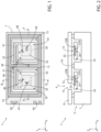
Figure 1 shows a top-plan view of a MEMS pressure sensor, according to one embodiment; -
Figure 2 shows a cross-section of the MEMS pressure sensor ofFigure 1 , along a section line II-II ofFigure 1 ; -
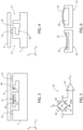
Figure 3 shows a cross-section of a portion of the MEMS pressure sensor ofFigure 1 , along a section line III-III ofFigure 1 ; -
Figure 4 shows a cross-section of a different portion of the MEMS pressure sensor ofFigure 1 , along a section line IV-IV ofFigure 1 ; -
Figure 5 shows a circuit diagram of a detection circuit coupeable to the MEMS pressure sensor ofFigure 1 ; -
Figure 6 shows a simplified view of a portion of the MEMS pressure sensor ofFigure 1 , in use; -
Figure 7 shows a cross-section of a MEMS pressure sensor, according to a different embodiment; and -
Figure 8 shows a circuit diagram of a detection circuit coupeable to a MEMS pressure sensor, according to one embodiment. - The following description refers to the arrangement shown in the attached Figures; consequently, expressions such as "above", "below", "lower", "upper", "right", "left", "top", "bottom", and the like, relate to the attached Figures and should not be interpreted in a limiting manner.
-
Figures 1 and 2 show apressure sensor 1, hereinafter also simply referred to assensor 1, in a Cartesian reference system XYZ having a first axis X, a second axis Y and a third axis Z. - The
sensor 1 is of MEMS type. - The
sensor 1 may be manufactured through micro- and nano-machining techniques known per se, for example starting from a wafer of semiconductor material, in particular silicon, and subsequent processing steps, for example including lithography, chemical etching, growth, annealing, dicing, bonding, etc., typical of the semiconductor industry. - The
sensor 1 is configured to detect an external pressure Pext. - The
sensor 1 is formed in abody 5 comprising alower substrate 7 and anupper substrate 9 mutually bonded through abonding region 10. - The
lower substrate 7 and theupper substrate 9 are of semiconductor material, in particular silicon. However, thelower substrate 7 and theupper substrate 9 may be of different material or comprise portions or layers of different material, for example insulating material, depending on the specific manufacturing processes used. - The
bonding region 10 is of a material that allows a hermetic bonding to be obtained between thelower substrate 7 and theupper substrate 9. For example, thebonding region 10 may be of aluminum-germanium (Al-Ge). Bonding through Al-Ge may allow very low pressures to be obtained, for example even lower than 20 mbar. -
Figure 1 shows, for clarity, thesensor 1 without theupper substrate 9. - The
sensor 1 comprises afirst chamber 12 and asecond chamber 13 arranged in thebody 5. - The
first chamber 12 and thesecond chamber 13 are hermetically separated from each other by thebonding region 10. - In this embodiment, the
body 5 comprises anopening 15 that couples thefirst chamber 12 with the outside of thesensor 1. In other words, theopening 15 causes thefirst chamber 12 to be at the external pressure Pext. - In the embodiment shown, the
opening 15 extends through theupper substrate 9, throughout its thickness along the third axis Z. - The
sensor 1 further comprises afirst detection structure 18 arranged in thefirst chamber 12 and asecond detection structure 19 arranged in thesecond chamber 13. - In detail, in this embodiment, the first and the
second detection structures second chamber elastic elements - The first and the
second detection structures elastic elements lower substrate 7, through subsequent processing steps comprising lithography, growth, chemical etching, etc. - The
elastic element 21 extends into thefirst chamber 12 between thefirst detection structure 18 and thelower substrate 7. Theelastic element 22 extends into thesecond chamber 13 between thesecond detection structure 19 and thelower substrate 7. - The
elastic elements respective detection structure lower substrate 7. In this manner, thedetection structures body 5. - Shape and dimensions of the
elastic elements elastic elements - The
first detection structure 18 comprises a buriedcavity 24 that extends within thefirst detection structure 18 and amembrane 25 that faces the buriedcavity 24. - In detail, the
membrane 25 has alower surface 25A facing the buriedcavity 24 and anupper surface 25B facing thefirst chamber 12. - In practice, the buried
cavity 24 delimits themembrane 25 at the bottom and thefirst chamber 12 delimits themembrane 25 at the top. - Position of the buried
cavity 24 within thefirst detection structure 18 and dimensions of the buriedcavity 24 may be chosen, during the design step, depending on the desired dimensions of themembrane 25. For example, themembrane 25 may have a thickness, along the third axis Z, comprised for example between 2 µm and 20 pm, and an area, measured in an XY plane, comprised between 40x40 µm2 and 600x600 µm2. - The
second detection structure 19 comprises a buriedcavity 30 that extends within thesecond detection structure 19 and amembrane 32 that faces the buriedcavity 30. - In detail, the
membrane 32 has alower surface 32A facing the buriedcavity 30 and anupper surface 32B facing thesecond chamber 13. - In practice, the buried
cavity 30 delimits themembrane 32 at the bottom and thesecond chamber 13 delimits themembrane 32 at the top. - Position of the buried
cavity 30 within thesecond detection structure 19 and dimensions of the buriedcavity 30 may be chosen, during the design step, depending on the desired dimensions of themembrane 32. For example, themembrane 32 may have a thickness, along the third axis Z, comprised for example between 2 µm and 20 pm, and an area, measured in the XY plane, comprised between 40x40 µm2 and 600x600 µm2. - In particular, the first and the
second detection structures membranes sensor 1 to be improved. - The
sensor 1 further comprises achannel 40 that extends into thebody 5 between the buriedcavity 24 and thesecond chamber 13 and achannel 41 that extends into thebody 5 between the buriedcavity 30 and thefirst chamber 12. - The
channel 40, details of which are shown inFigures 3 and 4 , is open at a first end on the buriedcavity 24 and at a second end on thesecond chamber 13. - In practice, the
channel 40 causes the buriedcavity 24 and thesecond chamber 13 to be at a same pressure P1. - The
channel 41 is open at a first end on the buriedcavity 30 and at a second end on thefirst chamber 12. - In practice, the
channel 41 causes the buriedcavity 30 and thefirst chamber 12 to be at a same pressure P2, which here is equal to the external pressure Pext. - In detail, the
channel 40 extends, starting from the buriedcavity 24, buried within thefirst detection structure 18, theelastic element 21 and part of thelower substrate 7, towards thesecond chamber 13. - In this embodiment, the
channel 40 comprises a via 43 that extends, along the third axis Z, from a surface of thelower substrate 7 which faces thesecond chamber 13 towards the inside of thelower substrate 7. In practice, the via 43 may fluidically couple the buried portion of thechannel 40 with thesecond chamber 13. - In detail, the
channel 41 extends, starting from the buriedcavity 30, buried within thesecond detection structure 19, theelastic element 22 and part of thelower substrate 7, towards thefirst chamber 12. - In this embodiment, the
channel 41 comprises a via 44 that extends, along the third axis Z, from a surface of thelower substrate 7 which faces thefirst chamber 12 towards the inside of thelower substrate 7. In practice, the via 44 may fluidically couple the buried portion of thechannel 41 with thefirst chamber 12. - The buried
cavities channels EP1577656 . - The
vias elastic elements detection structures - The
sensor 1 further comprises one or more transduction elements, here twopiezoresistors first detection structure 18 and one or more transduction elements, here twopiezoresistors second detection structure 19. - The
piezoresistors membrane 25. - In detail, the
piezoresistors membrane 25. - In particular, the resistances R1, R3 are sensitive both to the direction (upwards or downwards along the third axis Z) and to the extent of the deformation of the
membrane 25. - In this embodiment, the
piezoresistors membrane 25, a variation having sign opposite to each other. - For example, in response to a downward deformation of the
membrane 25, thepiezoresistor 47 may be configured to undergo a positive variation (increase) of the respective resistance R3 and thepiezoresistor 46 may be configured to undergo a negative variation (decrease) of the respective resistance R1. - The
piezoresistors membrane 32. - In detail, the
piezoresistors membrane 32. - In particular, the resistances R2, R4 are sensitive both to the direction (upwards or downwards along the third axis Z) and to the extent of the deformation of the
membrane 32. - In this embodiment, the
piezoresistors membrane 32, a variation having sign opposite to each other. For example, in response to an upward deformation of themembrane 32, thepiezoresistor 48 may be configured to undergo a positive variation (increase) of the respective resistance R2 and thepiezoresistor 49 may be configured to undergo a negative variation (decrease) of the respective resistance R4. - The
sensor 1 also comprises electrical connection means, comprisingcontact pads 50 and metal connection tracks (not shown here), which allow the electrical connection of thesensor 1, in particular of the transduction elements 46-49, to an electrical detection circuit for reading the resistances R1-R4. -
Figure 5 shows an embodiment of the detection circuit, here indicated by 50, wherein the piezoresistors 46-49 are electrically coupled to each other in a Wheatstone bridge configuration between a supply voltage Vcc and ground GND. - In particular, the
piezoresistor 46 and thepiezoresistor 47 form a half-bridge and are connected in series between the supply voltage Vcc and the ground GND. Thepiezoresistor 48 and thepiezoresistor 49 form a half-bridge and are connected in series between the supply voltage Vcc and the ground GND. - An
operational amplifier 52 is coupled to the piezoresistors 46-49 and provides a voltage Vout. - In use, in presence of the external pressure Pext to be measured, the pressure P2 of the
first chamber 12 and the buriedcavity 30 is equal to the external pressure Pext. - Consequently, between the
upper surface 25B and thelower surface 25A of the membrane 25 a pressure difference Pext - P1 is present, and between theupper surface 32B and thelower surface 32A of the membrane 32 a pressure difference P1 - Pext is present. - In practice, the
membranes -
Figure 6 shows an example where Pext = P2 > P1. In this case, themembrane 25 undergoes a downward deformation, while themembrane 32 undergoes an upward deformation. - The Wheatstone bridge configuration of the transduction elements 46-49 allows a differential detection of the pressure Pext to be obtained; therefore, any spurious-type mechanical stresses that may affect the first and the
second detection structures sensor 1 may have a high rejection of also internal undesired mechanical stimuli. Furthermore, bothmembranes membranes sensor 1 may therefore have a high detection sensitivity. -
Figure 7 shows a schematic cross-section of aMEMS pressure sensor 100, according to a different embodiment. Thesensor 100 has a general structure similar to that of thesensor 1; consequently, common elements are indicated by the same reference numerals and are not further described in detail. - The
sensor 100 comprises thebody 5 having thelower substrate 7 and an upper substrate, here indicated by 109, mutually bonded through thebonding region 10. - The
sensor 100 has the first and thesecond chambers second detection structure - Also in this embodiment, the
first detection structure 18 is a structure suspended through theelastic element 21 and comprises the buriedcavity 24 and themembrane 25; and thesecond detection structure 19 is a structure suspended through theelastic element 22 and comprises the buriedcavity 30 and themembrane 32. - Also here, the
first chamber 12 and the buriedcavity 30 are fluidically coupled by thechannel 40, and thesecond chamber 13 and the buriedcavity 24 are fluidically coupled by thechannel 41. - In this embodiment, the
opening 15 is a first opening of theupper substrate 109 and theupper substrate 109 also comprises asecond opening 115 on thesecond chamber 13. - Although not shown, transduction elements are coupled to the
membranes sensor 1. - In practice, in this embodiment, the
sensor 100 may be used as a differential pressure sensor between two external pressures Pext, Pext'. - In fact, here, the
first chamber 12 and the buriedcavity 30 are at the pressure Pext, and thesecond chamber 13 and the buriedcavity 24 are at the pressure Pext'. - Finally, it is clear that modifications and variations may be made to the
sensors - For example, the
openings lower substrate 7 and not through theupper substrate - For example, the
detection structures membranes elastic elements - The
membranes - For example, the
membranes - For example, the
detection structures body 5, in particular with thelower substrate 7. - For example, the pressure sensor may comprise one or more getter layers arranged on one or more walls of one or more of the
chambers cavities Figure 1 , a getter layer may be arranged on the (lower) internal wall of theupper substrate 9 which faces thesecond chamber 13, so that the pressure P1 is as low as possible. - For example, the transduction elements 46-49 may be based on a different transduction principle, for example piezoelectric, capacitive, etc., to detect the deformation of the
membranes - The present pressure sensor may have a different number of transduction elements, for example one for each of the
membranes - For example,
Figure 8 shows a different embodiment of the detection circuit, here indicated by 150, which may be used in case the present sensor has only one transduction element 152 coupled to themembrane 25 and only one transduction element 153 coupled to themembrane 32. - The transduction elements 152, 153 are piezoresistors having resistance R1 and, respectively, R2.
- The piezoresistors 152, 153 are sensitive to the direction along the third axis Z of the deformation of the
respective membrane respective membrane respective membrane - The
detection circuit 150 is an Anderson loop wherein the piezoresistors 152, 153 are arranged in series with each other. - In detail, the
detection circuit 150 comprises acurrent generator 155 which provides a reading current to the piezoresistors 152, 153; anoperational amplifier 156 coupled at input to the piezoresistor 152; anoperational amplifier 157 coupled at input to the piezoresistor 153; and anoperational amplifier 158 coupled to the outputs of theoperational amplifiers operational amplifier 158 operates as a subtractor that cancels any common mode stress components that affect the variation of the resistances R1, R2. - In this manner, the output voltage Vout is only a function of the external pressure to be measured and, at least as a first approximation, independent of spurious mechanical stresses.
- The
electrical detection circuits - The electrical connections among the transduction elements may be formed in the die wherein the transduction elements are formed, or in the die wherein the detection circuit is formed.
- Finally, the different embodiments described above may be combined to provide further solutions.
Claims (11)
- A pressure sensor (1; 100) comprising:a body (5) having a first chamber (12) and a second chamber (13) hermetically separated from the first chamber;a first detection structure (18) arranged in the first chamber (12), comprising a first deformable element (25) and a first buried cavity (24) within the first detection structure, wherein the first deformable element is configured to undergo a deformation as a function of a pressure difference between the first chamber and the first buried cavity;a second detection structure (19) arranged in the second chamber (13), comprising a second deformable element (32) and a second buried cavity (30) within the second detection structure, wherein the second deformable element is configured to undergo a deformation as a function of a pressure difference between the second chamber and the second buried cavity;a first channel (40, 43) extending into the body (5) and configured to fluidically couple the first buried cavity (24) with the second chamber (13); anda second channel (41, 44) extending into the body (5) and configured to fluidically couple the second buried cavity (30) with the first chamber (12).
- The pressure sensor according to the preceding claim, wherein the first deformable element (25) has a first face (25A) facing the first buried cavity (24) and a second face (25B) opposite to the first face and facing the first chamber (12), and wherein the second deformable element (32) has a first face (32A) facing the second buried cavity (30) and a second face (32B) opposite to the first face and facing the second chamber (13).
- The pressure sensor according to claim 1 or 2, wherein the first detection structure (18) is a structure suspended in the first chamber (12) and/or the second detection structure (19) is a structure suspended in the second chamber (13) .
- The pressure sensor according to any of the preceding claims, comprising at least one opening (15; 115) that extends through the body (5) and is configured to couple one of the first and the second chambers with an external pressure (Pext, Pext').
- The pressure sensor according to the preceding claim, wherein the at least one opening is a first opening (15) configured to fluidically couple the first chamber (12) with the external pressure (Pext), the sensor further comprising a second opening (115) extending through the body (5) and configured to fluidically couple the second chamber (13) with a second external pressure (Pext').
- The pressure sensor according to any of the preceding claims, wherein the body (5) comprises a lower substrate (7), an upper substrate (9; 109) and a bonding region (10) configured to hermetically couple the upper substrate with the lower substrate.
- The pressure sensor according to any of the preceding claims, further comprising at least one first transduction element (46, 47; 152) configured to detect the deformation of the first deformable element (25), and at least one second transduction element (48, 49; 153) configured to detect the deformation of the second deformable element (32).
- The pressure sensor according to the preceding claim, wherein the at least one first transduction element (46, 47; 152) is sensitive to the direction of the deformation of the first deformable element (25) and the at least one second transduction element (48, 49; 153) is sensitive to the direction of the deformation of the second deformable element (32) .
- The pressure sensor according to claim 7 or 8, wherein the at least one first transduction element and/or the at least one second transduction element are piezoresistors.
- The pressure sensor according to any of the preceding claims, further comprising a detection circuit (50; 150) configured to perform a differential reading of the deformation of the first deformable element (25) and the second deformable element (32).
- The pressure sensor according to any of the preceding claims, wherein the pressure sensor is of MEMS type.
Applications Claiming Priority (1)
| Application Number | Priority Date | Filing Date | Title |
|---|---|---|---|
| IT102023000022215A IT202300022215A1 (en) | 2023-10-24 | 2023-10-24 | PRESSURE SENSOR WITH IMPROVED REJECTION OF UNWANTED STIMULI |
Publications (1)
| Publication Number | Publication Date |
|---|---|
| EP4545927A1 true EP4545927A1 (en) | 2025-04-30 |
Family
ID=89321487
Family Applications (1)
| Application Number | Title | Priority Date | Filing Date |
|---|---|---|---|
| EP24206565.4A Pending EP4545927A1 (en) | 2023-10-24 | 2024-10-15 | Pressure sensor having improved rejection of undesired stimuli |
Country Status (4)
| Country | Link |
|---|---|
| US (1) | US20250130129A1 (en) |
| EP (1) | EP4545927A1 (en) |
| CN (1) | CN119873724A (en) |
| IT (1) | IT202300022215A1 (en) |
Citations (3)
| Publication number | Priority date | Publication date | Assignee | Title |
|---|---|---|---|---|
| EP1577656A1 (en) | 2004-03-19 | 2005-09-21 | STMicroelectronics S.r.l. | Method for manufacturing a semiconductor pressure sensor |
| EP3210934A1 (en) | 2016-02-25 | 2017-08-30 | STMicroelectronics Srl | Micro-electro-mechanical type pressure device having low sensitivity to temperature |
| US20180148323A1 (en) | 2016-11-30 | 2018-05-31 | Stmicroelectronics S.R.L. | Multi-device transducer modulus, electronic apparatus including the transducer modulus and method for manufacturing the transducer modulus |
-
2023
- 2023-10-24 IT IT102023000022215A patent/IT202300022215A1/en unknown
-
2024
- 2024-10-14 US US18/915,158 patent/US20250130129A1/en active Pending
- 2024-10-15 EP EP24206565.4A patent/EP4545927A1/en active Pending
- 2024-10-21 CN CN202411469187.XA patent/CN119873724A/en active Pending
Patent Citations (3)
| Publication number | Priority date | Publication date | Assignee | Title |
|---|---|---|---|---|
| EP1577656A1 (en) | 2004-03-19 | 2005-09-21 | STMicroelectronics S.r.l. | Method for manufacturing a semiconductor pressure sensor |
| EP3210934A1 (en) | 2016-02-25 | 2017-08-30 | STMicroelectronics Srl | Micro-electro-mechanical type pressure device having low sensitivity to temperature |
| US20180148323A1 (en) | 2016-11-30 | 2018-05-31 | Stmicroelectronics S.R.L. | Multi-device transducer modulus, electronic apparatus including the transducer modulus and method for manufacturing the transducer modulus |
Also Published As
| Publication number | Publication date |
|---|---|
| IT202300022215A1 (en) | 2025-04-24 |
| CN119873724A (en) | 2025-04-25 |
| US20250130129A1 (en) | 2025-04-24 |
Similar Documents
| Publication | Publication Date | Title |
|---|---|---|
| Eaton et al. | Micromachined pressure sensors: review and recent developments | |
| US8220330B2 (en) | Vertically integrated MEMS sensor device with multi-stimulus sensing | |
| Diem et al. | SOI'SIMOX'; from bulk to surface micromachining, a new age for silicon sensors and actuators | |
| EP3252449B1 (en) | Miniaturized load sensor device having low sensitivity to thermo-mechanical packaging stress, in particular force and pressure sensor | |
| US7093493B2 (en) | Pressure sensor having a silicon chip on a steel diaphragm | |
| US8387464B2 (en) | Laterally integrated MEMS sensor device with multi-stimulus sensing | |
| US8569092B2 (en) | Method for fabricating a microelectromechanical sensor with a piezoresistive type readout | |
| JP6053357B2 (en) | Pressure measuring device with optimized sensitivity | |
| US20150268115A1 (en) | Microelectromechanical and/or nanoelectromechanical differential pressure measurement sensor | |
| US9686864B2 (en) | Device including interposer between semiconductor and substrate | |
| JP2001523814A (en) | Micromechanical differential pressure sensor device | |
| US11697586B2 (en) | Surface micromechanical element and method for manufacturing the same | |
| CN115452207B (en) | A differential capacitive MEMS pressure sensor and its manufacturing method | |
| JP6258977B2 (en) | Sensor and manufacturing method thereof | |
| US20250130129A1 (en) | Pressure sensor having improved rejection of undesired stimuli | |
| JP2001524212A (en) | Batch assembled semiconductor thin film pressure sensor and method of manufacturing the same | |
| CN104603936B (en) | The semiconductor of substrate is fixed to via the hole in substrate | |
| JP3368744B2 (en) | Vibration acceleration sensor | |
| US10647568B2 (en) | Micromechanical component including diaphragm, manufacturing method for such a component and method for operating a pressure sensor | |
| JPH10142086A (en) | Semiconductor pressure sensor, method of manufacturing the same, and differential pressure transmitter using the same | |
| CN116609550B (en) | MEMS accelerometer and preparation method thereof | |
| US11879800B2 (en) | MEMS strain gauge pressure sensor with mechanical symmetries | |
| Li et al. | Enhanced Bulk Micromachining Based on MIS Process | |
| WO2013180696A1 (en) | Device including substrate that absorbs stresses | |
| WO2021005394A1 (en) | Pressure measurement sensor and manufacturing process of a differential pressure measurement sensor |
Legal Events
| Date | Code | Title | Description |
|---|---|---|---|
| PUAI | Public reference made under article 153(3) epc to a published international application that has entered the european phase |
Free format text: ORIGINAL CODE: 0009012 |
|
| STAA | Information on the status of an ep patent application or granted ep patent |
Free format text: STATUS: THE APPLICATION HAS BEEN PUBLISHED |
|
| AK | Designated contracting states |
Kind code of ref document: A1 Designated state(s): AL AT BE BG CH CY CZ DE DK EE ES FI FR GB GR HR HU IE IS IT LI LT LU LV MC ME MK MT NL NO PL PT RO RS SE SI SK SM TR |
|
| STAA | Information on the status of an ep patent application or granted ep patent |
Free format text: STATUS: REQUEST FOR EXAMINATION WAS MADE |
|
| 17P | Request for examination filed |
Effective date: 20251028 |
|
| GRAP | Despatch of communication of intention to grant a patent |
Free format text: ORIGINAL CODE: EPIDOSNIGR1 |
|
| STAA | Information on the status of an ep patent application or granted ep patent |
Free format text: STATUS: GRANT OF PATENT IS INTENDED |
|
| INTG | Intention to grant announced |
Effective date: 20260216 |
|
| RAP3 | Party data changed (applicant data changed or rights of an application transferred) |
Owner name: STMICROELECTRONICS INTERNATIONAL N.V. |