EP4542654A1 - A semiconductor switching device implementing an edge termination structure - Google Patents
A semiconductor switching device implementing an edge termination structure Download PDFInfo
- Publication number
- EP4542654A1 EP4542654A1 EP23204901.5A EP23204901A EP4542654A1 EP 4542654 A1 EP4542654 A1 EP 4542654A1 EP 23204901 A EP23204901 A EP 23204901A EP 4542654 A1 EP4542654 A1 EP 4542654A1
- Authority
- EP
- European Patent Office
- Prior art keywords
- type
- region
- switching device
- semiconductor switching
- charge carriers
- Prior art date
- Legal status (The legal status is an assumption and is not a legal conclusion. Google has not performed a legal analysis and makes no representation as to the accuracy of the status listed.)
- Pending
Links
Images



Classifications
-
- H—ELECTRICITY
- H10—SEMICONDUCTOR DEVICES; ELECTRIC SOLID-STATE DEVICES NOT OTHERWISE PROVIDED FOR
- H10D—INORGANIC ELECTRIC SEMICONDUCTOR DEVICES
- H10D62/00—Semiconductor bodies, or regions thereof, of devices having potential barriers
- H10D62/10—Shapes, relative sizes or dispositions of the regions of the semiconductor bodies; Shapes of the semiconductor bodies
- H10D62/102—Constructional design considerations for preventing surface leakage or controlling electric field concentration
- H10D62/103—Constructional design considerations for preventing surface leakage or controlling electric field concentration for increasing or controlling the breakdown voltage of reverse-biased devices
- H10D62/105—Constructional design considerations for preventing surface leakage or controlling electric field concentration for increasing or controlling the breakdown voltage of reverse-biased devices by having particular doping profiles, shapes or arrangements of PN junctions; by having supplementary regions, e.g. junction termination extension [JTE]
- H10D62/106—Constructional design considerations for preventing surface leakage or controlling electric field concentration for increasing or controlling the breakdown voltage of reverse-biased devices by having particular doping profiles, shapes or arrangements of PN junctions; by having supplementary regions, e.g. junction termination extension [JTE] having supplementary regions doped oppositely to or in rectifying contact with regions of the semiconductor bodies, e.g. guard rings with PN or Schottky junctions
-
- H—ELECTRICITY
- H10—SEMICONDUCTOR DEVICES; ELECTRIC SOLID-STATE DEVICES NOT OTHERWISE PROVIDED FOR
- H10D—INORGANIC ELECTRIC SEMICONDUCTOR DEVICES
- H10D62/00—Semiconductor bodies, or regions thereof, of devices having potential barriers
- H10D62/10—Shapes, relative sizes or dispositions of the regions of the semiconductor bodies; Shapes of the semiconductor bodies
- H10D62/102—Constructional design considerations for preventing surface leakage or controlling electric field concentration
- H10D62/103—Constructional design considerations for preventing surface leakage or controlling electric field concentration for increasing or controlling the breakdown voltage of reverse-biased devices
- H10D62/105—Constructional design considerations for preventing surface leakage or controlling electric field concentration for increasing or controlling the breakdown voltage of reverse-biased devices by having particular doping profiles, shapes or arrangements of PN junctions; by having supplementary regions, e.g. junction termination extension [JTE]
- H10D62/106—Constructional design considerations for preventing surface leakage or controlling electric field concentration for increasing or controlling the breakdown voltage of reverse-biased devices by having particular doping profiles, shapes or arrangements of PN junctions; by having supplementary regions, e.g. junction termination extension [JTE] having supplementary regions doped oppositely to or in rectifying contact with regions of the semiconductor bodies, e.g. guard rings with PN or Schottky junctions
- H10D62/107—Buried supplementary regions, e.g. buried guard rings
-
- H—ELECTRICITY
- H10—SEMICONDUCTOR DEVICES; ELECTRIC SOLID-STATE DEVICES NOT OTHERWISE PROVIDED FOR
- H10D—INORGANIC ELECTRIC SEMICONDUCTOR DEVICES
- H10D62/00—Semiconductor bodies, or regions thereof, of devices having potential barriers
- H10D62/10—Shapes, relative sizes or dispositions of the regions of the semiconductor bodies; Shapes of the semiconductor bodies
- H10D62/124—Shapes, relative sizes or dispositions of the regions of semiconductor bodies or of junctions between the regions
- H10D62/126—Top-view geometrical layouts of the regions or the junctions
- H10D62/127—Top-view geometrical layouts of the regions or the junctions of cellular field-effect devices, e.g. multicellular DMOS transistors or IGBTs
-
- H—ELECTRICITY
- H10—SEMICONDUCTOR DEVICES; ELECTRIC SOLID-STATE DEVICES NOT OTHERWISE PROVIDED FOR
- H10D—INORGANIC ELECTRIC SEMICONDUCTOR DEVICES
- H10D64/00—Electrodes of devices having potential barriers
- H10D64/111—Field plates
-
- H—ELECTRICITY
- H10—SEMICONDUCTOR DEVICES; ELECTRIC SOLID-STATE DEVICES NOT OTHERWISE PROVIDED FOR
- H10D—INORGANIC ELECTRIC SEMICONDUCTOR DEVICES
- H10D64/00—Electrodes of devices having potential barriers
- H10D64/111—Field plates
- H10D64/112—Field plates comprising multiple field plate segments
-
- H—ELECTRICITY
- H10—SEMICONDUCTOR DEVICES; ELECTRIC SOLID-STATE DEVICES NOT OTHERWISE PROVIDED FOR
- H10D—INORGANIC ELECTRIC SEMICONDUCTOR DEVICES
- H10D12/00—Bipolar devices controlled by the field effect, e.g. insulated-gate bipolar transistors [IGBT]
- H10D12/411—Insulated-gate bipolar transistors [IGBT]
- H10D12/441—Vertical IGBTs
Definitions
- the present disclosure relates to a semiconductor switching device implementing an edge termination structure.
- Edge termination structures are intended to limit or to terminate the electric field within minimal length or for a given length of the termination, to increase the breakdown voltage (VBR) of a semiconductor switching device.
- edge termination structures are intended to minimize the electric field peaks that often are cause of reliability failures of the device.
- the electric field during the blocking state of an edge termination structure may still consist of maxima's and thus may still be the cause of reliability failures.
- a semiconductor switching device is proposed implementing an edge termination structure.
- the semiconductor switching device comprises a semiconductor die formed by a first region doped with a first type of charge carriers and the top section having a center area and a peripheral area surrounding the center area. At least one junction is provided in the center area of the semiconductor die, the junction being formed between a second region doped with a second type of charge carriers different from the first type of charge carriers, with the second region adjoining the first region.
- an edge termination structure is provided in the edge area and surrounds the center area.
- the edge termination structure is structured to prevent voltage breakdown during operation of the semiconductor switching device, and composed of at least one ring structure provided at the edge of the first region.
- the at least one ring structure is composed of a series of spaced apart concentric ring sections provided in the first region, each ring section being doped with the second type of charge carriers and being spaced apart by a spacing doped with the first type of charge carriers.
- the first type of charge carriers may be N-type carriers
- the second type of charge carriers may be P-type carriers.
- the reversed configuration, wherein the first type of charge carriers are P-type carriers and the second type of charge carriers are N-type carriers is equally appliable in achieving the desired effect of smoothening out electric field peaks and improving the VBR and the reliability.
- the second region is formed as a well in the first region. Accordingly, such device can be manufactured in a logical sequence of manufacturing steps.
- the number of subring sections is in the range of 3-10, in particular 3-8 and more in particular 3-5.
- the lateral width of a subring section maybe in the range of 3-10 ⁇ m, in particular 3-6 ⁇ m and preferably 4 ⁇ m.
- a spacing between adjacent subring sections may be in the range of 4-10 ⁇ m, preferably 6-10 ⁇ m.
- the termination structure comprises a metal field plate element on top of the main ring section extending to the spacing between the main ring sections.
- the metal FP structure can increase the reliability in cases of suboptimal charge shielding of passivation layers.
- the first type of charge carriers are N-type carriers
- the second type of charge carriers are logically P-type carriers.
- the reversed configuration, wherein the first type of charge carriers are P-type carriers and the second type of charge carriers are N-type carriers is equally appliable in all examples described in this application, as both configurations (NP or PN) achieve the desired effect of the disclosure.
- edge termination structures are intended to limit or to terminate the electric field within minimal length or for a given length of the termination, to increase the breakdown voltage (VBR) of a semiconductor switching device.
- edge termination structures are intended to minimize the electric field peaks that often are cause of reliability failures of the device.
- Reference numeral 10 denotes a semiconductor switching device, yet is functionality or manner of operation is not detailed further.
- the device 10 is formed of a semiconductor die 11.
- the die 11 is formed by a first region doped with a first type of charge carriers.
- the first type of charge carriers are N-type of charge carriers.
- the semiconductor switching device 10 has a center area denoted with reference numeral 10y and a peripheral area surrounding the center area 10y, with the peripheral area being denoted with reference numeral 10z.
- the center area 10y of the semiconductor die 11 may be provided with a junction usually being formed by a second region doped with a second type of charge carriers different from the first type of charge carriers, with the second region adjoining or above or on top of the first region.
- Reference numeral 13 may denote an edge termination structure that is provided in the edge area 10z and that surrounds the center area 10y of the semiconductor die 11.
- the edge termination structure 13 is structured to prevent voltage breakdown during operation of the semiconductor switching device 10, and composed of at least one ring structure 13, that is provided in the first region doped with a first type of charge carriers, here in this example P-type carriers.
- Each ring structure 13 may be electrically connected with a metal field plate element 14, the latter being placed on top of the ring structure 13.
- Reference numeral 16 denotes a polyamide humidity insulator, covering in an isolated manner the semiconductor die surface and the metal field plate elements 14.
- Reference numeral 12 may denote an electrode to apply a bias voltage.
- Figure 1B (accompanied by its detailed view C-C in Figure 1C ) show an example of an improved semiconductor switching device with an edge termination structure exhibiting an improved VBR and reliability.
- FIG. 1B and in its detailed enlargement C-C in Figure 1C corresponding technical features taken from Figure 1A are denoted with a similar numeral referencing.
- FIGs 1B and 1C an example of a semiconductor switching device according to the disclosure is denoted with reference numeral 100. It is formed of a semiconductor die 111 having a first region doped with a first type of charge carriers, which could be P-type or N-type.
- the center area of the semiconductor switching device 100 is denoted as 100y and a peripheral area 100z surrounding the center area 100y.
- the center area 100y of the semiconductor die 111 may be provided with a junction usually being formed by a second region doped with a second type of charge carriers different from the first type of charge carriers, with the second region adjoining the first region.
- the edge termination structure 113 of the disclosure is provided in the edge area 100z and surrounds in a similar fashion as in the prior art the center area 100y of the semiconductor die 111.
- the edge termination structure 113 according to the disclosure also prevents voltage breakdown during operation of the semiconductor switching device 100.
- the edge termination structure 113 is formed as a ring structure composed of a series of spaced apart concentric ring sections. Each individual concentric ring section is denoted with reference numerals 113 1 -..-113 3 -..-113 n .
- the various individual concentrically oriented ring sections 113 n are present in the first region, and are each being doped with the second type of charge carriers. As seen in more detail in Figure 1C , the individual concentrically oriented ring sections 113 n are spaced apart by spacings 120. See also the top view in Figure 2 .
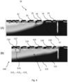
- FIG. 4A and 4B show the electric field distribution profiles E for the standard structure of Figure 1A and for the example of the disclosure, Figure 1B , both at 1200V.
- Figure 4B depicting an example according to the disclosure, the generated electric field E is spread across the semiconductor die structure 111, as compared with the known state-of-the-art device 10 as depicted in Figure 1A .
- An overall improvement in VBR was observed for the implant dose of 5 ⁇ 10 12 and 1.5 ⁇ 10 13 .
- the reliability of the new configuration of the disclosure is also expected to be better.
- the semiconductor switching device 100 according to the disclosure becomes robust since the sensitive high electric field peaks are pushed away from the surface and their amplitude is diminished.
- the electric field during the blocking state of a FP structure ( Figures 1B and 1C ) consists of maxima's in the gaps 120 between the concentric ring sections 113 n , and minima's, inside the concentric ring sections 113 n . It also includes another maxima in the large gaps between rings 113.
- the known single p-implanted ring structure 13 is substituted with 3-5 individual concentric ring sections 113 n with a ⁇ 3-10 ⁇ m width of ring sections 113 n and 4-10 ⁇ m width of spacings 120. After diffusion, these concentric ring sections 113 n become partially inter-diffused spreading the doping evenly inside the ring sections 113 n .
- each ring structure 113 may be electrically connected with a metal field plate element 114, the latter being placed on top of the ring structure 113.
- each metal field plate element 114 may be electrically connected at one of the spaced apart concentric ring sections 113 n , the contact section is denoted with reference numeral 117, see in particular the more detailed Figure 1C .
- the second region is formed as a well in the first region. Accordingly, such device can be manufactured in a logical sequence of manufacturing steps.
- the number n of ring sections 113 n is in the range of 3-10, in particular 3-8 and more in particular 3-5.
- the lateral width of a ring section 113 n maybe in the range of 3-10 ⁇ m, in particular 3-6 ⁇ m and preferably 4 ⁇ m.
- a spacing 120 between adjacent ring sections 113 n may be in the range of 4-10 ⁇ m, preferably 6-10 ⁇ m.
Landscapes
- Electrodes Of Semiconductors (AREA)
- Thyristors (AREA)
- Semiconductor Integrated Circuits (AREA)
Abstract
According to a first example of the disclosure, a semiconductor switching device implementing an edge termination structure is proposed. The semiconductor switching device comprises a semiconductor die formed by a first region (111) doped with a first type of charge carriers and having a center area (100y) and a peripheral area (100z) surrounding the center area, and at least one junction provided in the center area of the semiconductor die, the junction being formed with respect to a second region doped with a second type of charge carriers different from the first type of charge carriers, with the second region adjoining the first region.
An edge termination structure is provided in the edge area (100z) and surrounding the center area (100y), and structured to prevent voltage breakdown during operation of the semiconductor switching device, the edge termination structure being composed of are least one ring structure (113, 120) provided in the first region, wherein the at least ring one structure is composed of a series of spaced apart concentric ring sections (113) provided in the first region, each ring section being doped with the second type of charge carriers and being spaced apart by a spacing (120) doped with the first type of charge carriers. Each ring section is connected to a field plate (114).
Description
- The present disclosure relates to a semiconductor switching device implementing an edge termination structure.
- Edge termination structures are intended to limit or to terminate the electric field within minimal length or for a given length of the termination, to increase the breakdown voltage (VBR) of a semiconductor switching device. In particular edge termination structures are intended to minimize the electric field peaks that often are cause of reliability failures of the device. However, depending on the doping profile and configuration, the electric field during the blocking state of an edge termination structure may still consist of maxima's and thus may still be the cause of reliability failures.
- Accordingly, it is a goal of the present disclosure to provide an improved semiconductor switching device with an edge termination structure with an improved VBR and reliability.
- According to a first example of the disclosure, a semiconductor switching device is proposed implementing an edge termination structure. The semiconductor switching device comprises a semiconductor die formed by a first region doped with a first type of charge carriers and the top section having a center area and a peripheral area surrounding the center area. At least one junction is provided in the center area of the semiconductor die, the junction being formed between a second region doped with a second type of charge carriers different from the first type of charge carriers, with the second region adjoining the first region.
- In addition, an edge termination structure is provided in the edge area and surrounds the center area. The edge termination structure is structured to prevent voltage breakdown during operation of the semiconductor switching device, and composed of at least one ring structure provided at the edge of the first region.
- The at least one ring structure is composed of a series of spaced apart concentric ring sections provided in the first region, each ring section being doped with the second type of charge carriers and being spaced apart by a spacing doped with the first type of charge carriers.
- Accordingly, with the substitution of the currently implemented each wide ring with multiple narrow subrings which are provided concentric to each other the implantation (doping) profiles of the relevant charge carriers are spread smoothly in a lateral direction, The resulting electric field, which is a function of the doping, is smoothed out to get the advantages of the VLD-like profile within each ring. Accordingly, any electric field peaks that occur within the spacings at the various junctions of the ring sections are further reduced and thereby the VBR and the reliability are improved.
- It should be noted, that the first type of charge carriers may be N-type carriers, whereas the second type of charge carriers may be P-type carriers. However, the reversed configuration, wherein the first type of charge carriers are P-type carriers and the second type of charge carriers are N-type carriers is equally appliable in achieving the desired effect of smoothening out electric field peaks and improving the VBR and the reliability.
- In an example, the second region is formed as a well in the first region. Accordingly, such device can be manufactured in a logical sequence of manufacturing steps.
- In an advantageous example, the number of subring sections is in the range of 3-10, in particular 3-8 and more in particular 3-5.
- In particular, the lateral width of a subring section maybe in the range of 3-10 µm, in particular 3-6 µm and preferably 4 µm.
- Likewise, a spacing between adjacent subring sections may be in the range of 4-10 µm, preferably 6-10 µm.
- In a further advantageous example, the termination structure comprises a metal field plate element on top of the main ring section extending to the spacing between the main ring sections. The metal FP structure can increase the reliability in cases of suboptimal charge shielding of passivation layers.
- The disclosure will now be discussed with reference to the drawings, which show in:
-
Figure 1A a semiconductor switching device implementing an edge termination structure according to the state of the art; -
Figure 1B a field plate edge termination structure according to an example of the disclosure; -
Figure 1C a detailed view of the example ofFigure 1B ; -
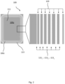
Figure 2 a top view of the example ofFigure 1B and1C ; -
Figure 3 an improved breakdown voltage (VBR) for the Field plate termination example according to the disclosure compared with the state of the art -
Figure 4A an electric field distribution profile for the standard structure ofFigure 1A at 1200V; -
Figure 4B an electric field distribution profile for the example of the disclosure at 1200V. - For a proper understanding of the disclosure, in the detailed description below corresponding elements or parts of the disclosure will be denoted with identical reference numerals in the drawings.
- Throughout the following detailed description it is understood, that the first type of charge carriers are N-type carriers, and the second type of charge carriers are logically P-type carriers. However, the reversed configuration, wherein the first type of charge carriers are P-type carriers and the second type of charge carriers are N-type carriers is equally appliable in all examples described in this application, as both configurations (NP or PN) achieve the desired effect of the disclosure.
- As outlined in the introductory part of this application, edge termination structures are intended to limit or to terminate the electric field within minimal length or for a given length of the termination, to increase the breakdown voltage (VBR) of a semiconductor switching device. In particular edge termination structures are intended to minimize the electric field peaks that often are cause of reliability failures of the device.
- An example as known in the prior art is detailed in
Figure 1A .Reference numeral 10 denotes a semiconductor switching device, yet is functionality or manner of operation is not detailed further. Thedevice 10 is formed of a semiconductor die 11. The die 11 is formed by a first region doped with a first type of charge carriers. For the sake of clarity and explanation of the disclosure, it is assumed that the first type of charge carriers are N-type of charge carriers. - The
semiconductor switching device 10 has a center area denoted withreference numeral 10y and a peripheral area surrounding thecenter area 10y, with the peripheral area being denoted withreference numeral 10z. - Although not relevant for a proper understanding of the disclosure, the
center area 10y of thesemiconductor die 11 may be provided with a junction usually being formed by a second region doped with a second type of charge carriers different from the first type of charge carriers, with the second region adjoining or above or on top of the first region. -
Reference numeral 13 may denote an edge termination structure that is provided in theedge area 10z and that surrounds thecenter area 10y of the semiconductor die 11. Theedge termination structure 13 is structured to prevent voltage breakdown during operation of thesemiconductor switching device 10, and composed of at least onering structure 13, that is provided in the first region doped with a first type of charge carriers, here in this example P-type carriers. Eachring structure 13 may be electrically connected with a metalfield plate element 14, the latter being placed on top of thering structure 13. - Between the
metal plate element 14 and the semiconductor surface, aninsulation layer 15 is provided.Reference numeral 16 denotes a polyamide humidity insulator, covering in an isolated manner the semiconductor die surface and the metalfield plate elements 14.Reference numeral 12 may denote an electrode to apply a bias voltage. -
Figure 1B (accompanied by its detailed view C-C inFigure 1C ) show an example of an improved semiconductor switching device with an edge termination structure exhibiting an improved VBR and reliability. - In
Figure 1B and in its detailed enlargement C-C inFigure 1C , corresponding technical features taken fromFigure 1A are denoted with a similar numeral referencing. InFigures 1B and1C an example of a semiconductor switching device according to the disclosure is denoted withreference numeral 100. It is formed of asemiconductor die 111 having a first region doped with a first type of charge carriers, which could be P-type or N-type. - The center area of the
semiconductor switching device 100 is denoted as 100y and aperipheral area 100z surrounding thecenter area 100y. Likewise, thecenter area 100y of thesemiconductor die 111 may be provided with a junction usually being formed by a second region doped with a second type of charge carriers different from the first type of charge carriers, with the second region adjoining the first region. - The
edge termination structure 113 of the disclosure is provided in theedge area 100z and surrounds in a similar fashion as in the prior art thecenter area 100y of thesemiconductor die 111. Theedge termination structure 113 according to the disclosure also prevents voltage breakdown during operation of thesemiconductor switching device 100. - Contrary to the prior art
edge termination structure 13, according to the present disclosure theedge termination structure 113 is formed as a ring structure composed of a series of spaced apart concentric ring sections. Each individual concentric ring section is denoted with reference numerals 1131-..-1133-..-113n. The various individual concentrically orientedring sections 113n are present in the first region, and are each being doped with the second type of charge carriers. As seen in more detail inFigure 1C , the individual concentricallyoriented ring sections 113n are spaced apart byspacings 120. See also the top view inFigure 2 . - By substituting of the single
wide ring 13 as in the prior art ofFigure 1A with multiplenarrow ring sections 113n which are provided concentric to each other in thesemiconductor die structure 111 the doping profiles of the relevant charge carriers are spread in a lateral direction as well as deeper into the semiconductor device, hence towards theouter periphery 100z of thesemiconductor switching device 100 as seen in a direction originating from thecenter area 100y towards theperipheral area 100z thereof. The resulting electric field, which is a function of the doping, is smoothed out to get the advantages of the VLD-like profile within the rings. Accordingly, large electric field peaks that occur within the wide spacings between therings 13, are further reduced and thereby the VBR and the reliability of thesemiconductor switching device 100 according to the disclosure are improved. - The above advantageous effects on the electric field are shown in
Figure 4A and 4B , showing the electric field distribution profiles E for the standard structure ofFigure 1A and for the example of the disclosure,Figure 1B , both at 1200V. InFigure 4B , depicting an example according to the disclosure, the generated electric field E is spread across thesemiconductor die structure 111, as compared with the known state-of-the-art device 10 as depicted inFigure 1A . - The configuration of the
edge termination structure 113 by means of multiplenarrow ring sections 113n results in the VBR increase, as shown inFigure 3 from 1348 V to 1500 V, which is considered an improvement of approx. 150 V (=10%) compared to the state of the art example (also depicted in the same graph). An overall improvement in VBR was observed for the implant dose of 5×10¹² and 1.5×10¹³. - The reliability of the new configuration of the disclosure, that is the substitution of the single
wide ring 13 as in the prior art with multiplenarrow ring sections 113n according to the disclosure, is also expected to be better. In cases of high humidity and cosmic ray events as well as in suboptimal passivation of external charges, thesemiconductor switching device 100 according to the disclosure becomes robust since the sensitive high electric field peaks are pushed away from the surface and their amplitude is diminished. - Resulting from this doping profile due to the multiple
concentric ring sections 113n the electric field during the blocking state of a FP structure (Figures 1B and1C ) consists of maxima's in thegaps 120 between theconcentric ring sections 113n, and minima's, inside theconcentric ring sections 113n. It also includes another maxima in the large gaps betweenrings 113. - In an FP example, the known single p-implanted
ring structure 13 is substituted with 3-5 individualconcentric ring sections 113n with a ~3-10µm width ofring sections 113n and 4-10 µm width ofspacings 120. After diffusion, theseconcentric ring sections 113n become partially inter-diffused spreading the doping evenly inside thering sections 113n. - Likewise, each
ring structure 113 may be electrically connected with a metalfield plate element 114, the latter being placed on top of thering structure 113. In more detail, each metalfield plate element 114 may be electrically connected at one of the spaced apartconcentric ring sections 113n, the contact section is denoted withreference numeral 117, see in particular the more detailedFigure 1C . - Similarly, between the
metal plate element 114 and (the first region doped with the first type of charge carriers of) the semiconductor die 111 aninsulation layer 115 is provided. Themetal plate structure 114 can increase the reliability in cases of suboptimal charge shielding of passivation layers. Also,reference numeral 116 denotes a passivation layer covering theinsulation layer 115 and the associated metalfield plate elements 114. Likewise,reference numeral 112 may denote a contact implant and an electrode to apply a bias voltage. - In an example, the second region is formed as a well in the first region. Accordingly, such device can be manufactured in a logical sequence of manufacturing steps.
- In an advantageous example, the number n of
ring sections 113n is in the range of 3-10, in particular 3-8 and more in particular 3-5. - In particular, the lateral width of a
ring section 113n maybe in the range of 3-10 µm, in particular 3-6 µm and preferably 4 µm. - Likewise, a spacing 120 between
adjacent ring sections 113n may be in the range of 4-10 µm, preferably 6-10 µm. - Aspects of the invention are set out in the accompanying independent claims. Combinations of features from the dependent and/or independent claims may be combined as appropriate and not merely as set out in the claims.
- The scope of the present disclosure includes any novel feature or combination of features disclosed therein either explicitly or implicitly or any generalisation thereof irrespective of whether or not it relates to the claimed invention or mitigate against any or all of the problems addressed by the present invention. The applicant hereby gives notice that new claims may be formulated to such features during prosecution of this application or of any such further application derived there from. In particular, with reference to the appended claims, features from dependent claims may be combined with those of the independent claims and features from respective independent claims may be combined in any appropriate manner and not merely in specific combinations enumerated in the claims.
- Features which are described in the context of separate embodiments may also be provided in combination in a single embodiment. Conversely, various features which are, for brevity, described in the context of a single embodiment, may also be provided separately or in any suitable sub combination.
- Term "comprising" does not exclude other elements or steps, the term "a" or "an" does not exclude a plurality. Reference signs in the claims shall not be construed as limiting the scope of the claims.
-
- 10
- semiconductor switching device according to the prior art
- 10y
- center area
- 10z
- peripheral area
- 11
- semiconductor die structure
- 12
- electrode
- 13
- edge termination structure
- 14
- metal field plate element
- 15
- insulation layer
- 16
- field shielding plate
- 100
- semiconductor switching device according to the disclosure
- 100y
- center area
- 100z
- peripheral area
- 111
- semiconductor die structure
- 112
- electrode
- 113
- edge termination structure according to the disclosure
- 113n
- spaced apart concentric ring sections
- 114
- metal field plate element
- 115
- insulation layer
- 116
- field shielding plate
- 117
- concentric ring section electrically connected with field shielding plate
- 120
- spacing or pitch
Claims (8)
- A semiconductor switching device implementing an edge termination structure, the semiconductor switching device comprising:a semiconductor die formed by a first region doped with a first type of charge carriers and having a center area and a peripheral area surrounding the center area,at least one junction provided in the center area of the semiconductor die, the junction being formed a second region doped with a second type of charge carriers different from the first type of charge carriers, with the second region adjoining the first region,an edge termination structure provided in the edge area and surrounding the center area, and structured to prevent voltage breakdown during operation of the semiconductor switching device, the edge termination structure being composed of at least one ring structure provided in the first region, whereinthe at least ring one structure is composed of a series of spaced apart concentric ring sections provided in the first region, each ring section being doped with the second type of charge carriers and being spaced apart by a spacing doped with the first type of charge carriers.
- The semiconductor switching device according to claim 1, wherein the first type of charge carriers are N-type carriers and the second type of charge carriers are P-type carriers.
- The semiconductor switching device according to claim 1, wherein the first type of charge carriers are P-type carriers and the second type of charge carriers are N-type carriers.
- The semiconductor switching device according to any one or more of the claims 1-3, wherein the second region is formed as a well in the first region.
- The semiconductor switching device according to any one or more of the claims 1-3, wherein the first region and the second region are formed as layers, with the first region layer extending over the second region layer.
- The semiconductor switching device according to any one or more of the claims 1-5, wherein the number of ring sections is in the range of 3-10, in particular 3-8 and more in particular 3-5.
- The semiconductor switching device according to any one or more of the claims 1-6, wherein a lateral width of a ring section is in the range of 3-10 µm, in particular 3-6 µm and preferably 4 µm.
- The semiconductor switching device according to any one or more of the claims 1-7, wherein a spacing between adjacent ring sections is in the range of 4-10 µm, preferably 6-10 µm.
Priority Applications (3)
| Application Number | Priority Date | Filing Date | Title |
|---|---|---|---|
| EP23204901.5A EP4542654A1 (en) | 2023-10-20 | 2023-10-20 | A semiconductor switching device implementing an edge termination structure |
| CN202411451588.2A CN119866040A (en) | 2023-10-20 | 2024-10-17 | Semiconductor switching device for implementing edge terminal structure |
| US18/919,768 US20250133782A1 (en) | 2023-10-20 | 2024-10-18 | Semiconductor switching device implementing an edge termination structure |
Applications Claiming Priority (1)
| Application Number | Priority Date | Filing Date | Title |
|---|---|---|---|
| EP23204901.5A EP4542654A1 (en) | 2023-10-20 | 2023-10-20 | A semiconductor switching device implementing an edge termination structure |
Publications (1)
| Publication Number | Publication Date |
|---|---|
| EP4542654A1 true EP4542654A1 (en) | 2025-04-23 |
Family
ID=88511204
Family Applications (1)
| Application Number | Title | Priority Date | Filing Date |
|---|---|---|---|
| EP23204901.5A Pending EP4542654A1 (en) | 2023-10-20 | 2023-10-20 | A semiconductor switching device implementing an edge termination structure |
Country Status (3)
| Country | Link |
|---|---|
| US (1) | US20250133782A1 (en) |
| EP (1) | EP4542654A1 (en) |
| CN (1) | CN119866040A (en) |
Citations (6)
| Publication number | Priority date | Publication date | Assignee | Title |
|---|---|---|---|---|
| US20090302376A1 (en) * | 2008-05-28 | 2009-12-10 | Kabushiki Kaisha Toshiba | Semiconductor device |
| WO2011013379A1 (en) * | 2009-07-31 | 2011-02-03 | Fuji Electric Systems Co., Ltd. | Semiconductor apparatus |
| US20190288062A1 (en) * | 2016-11-10 | 2019-09-19 | Rohm Co., Ltd. | Semiconductor device |
| US20200091282A1 (en) * | 2017-05-08 | 2020-03-19 | Rohm Co., Ltd. | Semiconductor device |
| US11227844B1 (en) * | 2018-10-09 | 2022-01-18 | National Technology & Engineering Solutions Of Sandia, Llc | Gallium nitride electromagnetic pulse arrestor |
| WO2023285133A1 (en) * | 2021-07-16 | 2023-01-19 | Rise Research Institutes of Sweden AB | Junction termination structure |
-
2023
- 2023-10-20 EP EP23204901.5A patent/EP4542654A1/en active Pending
-
2024
- 2024-10-17 CN CN202411451588.2A patent/CN119866040A/en active Pending
- 2024-10-18 US US18/919,768 patent/US20250133782A1/en active Pending
Patent Citations (6)
| Publication number | Priority date | Publication date | Assignee | Title |
|---|---|---|---|---|
| US20090302376A1 (en) * | 2008-05-28 | 2009-12-10 | Kabushiki Kaisha Toshiba | Semiconductor device |
| WO2011013379A1 (en) * | 2009-07-31 | 2011-02-03 | Fuji Electric Systems Co., Ltd. | Semiconductor apparatus |
| US20190288062A1 (en) * | 2016-11-10 | 2019-09-19 | Rohm Co., Ltd. | Semiconductor device |
| US20200091282A1 (en) * | 2017-05-08 | 2020-03-19 | Rohm Co., Ltd. | Semiconductor device |
| US11227844B1 (en) * | 2018-10-09 | 2022-01-18 | National Technology & Engineering Solutions Of Sandia, Llc | Gallium nitride electromagnetic pulse arrestor |
| WO2023285133A1 (en) * | 2021-07-16 | 2023-01-19 | Rise Research Institutes of Sweden AB | Junction termination structure |
Also Published As
| Publication number | Publication date |
|---|---|
| CN119866040A (en) | 2025-04-22 |
| US20250133782A1 (en) | 2025-04-24 |
Similar Documents
| Publication | Publication Date | Title |
|---|---|---|
| US4134123A (en) | High voltage Schottky barrier diode | |
| KR101679164B1 (en) | Reverse conducting power semiconductor device | |
| US4454527A (en) | Thyristor having controllable emitter short circuits and a method for its operation | |
| US11056582B2 (en) | Bidirectional phase controlled thyristor (BiPCT)—a new semiconductor device concept | |
| KR20000064647A (en) | Semiconductor devices | |
| WO1994016462A1 (en) | Spiral edge passivation structure for semiconductor devices | |
| US4132996A (en) | Electric field-controlled semiconductor device | |
| EP0143259B1 (en) | Composite type thyristor | |
| JP3853595B2 (en) | Semiconductor component having field forming region | |
| EP4542654A1 (en) | A semiconductor switching device implementing an edge termination structure | |
| JPS6243548B2 (en) | ||
| US5184198A (en) | Special geometry Schottky diode | |
| JP6736585B2 (en) | Thyristor with improved plasma spread | |
| CA1188820A (en) | Radiation-controllable thyristor | |
| US20240097048A1 (en) | Mps diode having non-uniformly spaced wells and method for manufacturing the same | |
| JP4696356B2 (en) | Semiconductor device | |
| EP0391337B1 (en) | Gate turn-off thyristor | |
| US20240014302A1 (en) | Bidirectional thyristor device with asymmetric characteristics | |
| CN120786913B (en) | Semiconductor device with a semiconductor layer having a plurality of semiconductor layers | |
| CN116057711A (en) | power semiconductor device | |
| KR20090113964A (en) | Manufacturing method of high voltage schottky barrier diode | |
| US20240097046A1 (en) | Mps diode having a non-uniformly doped region and method for manufacturing the same | |
| EP3925009B1 (en) | Integrated gate-commutated thyristor (igct) | |
| JPH02294073A (en) | Large blocking capacitance semiconductor device | |
| US20250261388A1 (en) | Semiconductor device |
Legal Events
| Date | Code | Title | Description |
|---|---|---|---|
| PUAI | Public reference made under article 153(3) epc to a published international application that has entered the european phase |
Free format text: ORIGINAL CODE: 0009012 |
|
| STAA | Information on the status of an ep patent application or granted ep patent |
Free format text: STATUS: THE APPLICATION HAS BEEN PUBLISHED |
|
| AK | Designated contracting states |
Kind code of ref document: A1 Designated state(s): AL AT BE BG CH CY CZ DE DK EE ES FI FR GB GR HR HU IE IS IT LI LT LU LV MC ME MK MT NL NO PL PT RO RS SE SI SK SM TR |
|
| STAA | Information on the status of an ep patent application or granted ep patent |
Free format text: STATUS: REQUEST FOR EXAMINATION WAS MADE |
|
| 17P | Request for examination filed |
Effective date: 20251023 |