EP4542644A1 - Semiconductor device with surrounding bump metallization and method therefor - Google Patents
Semiconductor device with surrounding bump metallization and method therefor Download PDFInfo
- Publication number
- EP4542644A1 EP4542644A1 EP24204783.5A EP24204783A EP4542644A1 EP 4542644 A1 EP4542644 A1 EP 4542644A1 EP 24204783 A EP24204783 A EP 24204783A EP 4542644 A1 EP4542644 A1 EP 4542644A1
- Authority
- EP
- European Patent Office
- Prior art keywords
- metal wall
- wall segments
- vertical metal
- sbm
- conductive layer
- Prior art date
- Legal status (The legal status is an assumption and is not a legal conclusion. Google has not performed a legal analysis and makes no representation as to the accuracy of the status listed.)
- Pending
Links
Images




Classifications
-
- H—ELECTRICITY
- H10—SEMICONDUCTOR DEVICES; ELECTRIC SOLID-STATE DEVICES NOT OTHERWISE PROVIDED FOR
- H10W—GENERIC PACKAGES, INTERCONNECTIONS, CONNECTORS OR OTHER CONSTRUCTIONAL DETAILS OF DEVICES COVERED BY CLASS H10
- H10W72/00—Interconnections or connectors in packages
- H10W72/20—Bump connectors, e.g. solder bumps or copper pillars; Dummy bumps; Thermal bumps
- H10W72/241—Dispositions, e.g. layouts
- H10W72/244—Dispositions, e.g. layouts relative to underlying supporting features, e.g. bond pads, RDLs or vias
-
- H—ELECTRICITY
- H10—SEMICONDUCTOR DEVICES; ELECTRIC SOLID-STATE DEVICES NOT OTHERWISE PROVIDED FOR
- H10W—GENERIC PACKAGES, INTERCONNECTIONS, CONNECTORS OR OTHER CONSTRUCTIONAL DETAILS OF DEVICES COVERED BY CLASS H10
- H10W90/00—Package configurations
- H10W90/701—Package configurations characterised by the relative positions of pads or connectors relative to package parts
-
- H—ELECTRICITY
- H10—SEMICONDUCTOR DEVICES; ELECTRIC SOLID-STATE DEVICES NOT OTHERWISE PROVIDED FOR
- H10W—GENERIC PACKAGES, INTERCONNECTIONS, CONNECTORS OR OTHER CONSTRUCTIONAL DETAILS OF DEVICES COVERED BY CLASS H10
- H10W70/00—Package substrates; Interposers; Redistribution layers [RDL]
- H10W70/60—Insulating or insulated package substrates; Interposers; Redistribution layers
- H10W70/62—Insulating or insulated package substrates; Interposers; Redistribution layers characterised by their interconnections
- H10W70/65—Shapes or dispositions of interconnections
-
- H—ELECTRICITY
- H10—SEMICONDUCTOR DEVICES; ELECTRIC SOLID-STATE DEVICES NOT OTHERWISE PROVIDED FOR
- H10W—GENERIC PACKAGES, INTERCONNECTIONS, CONNECTORS OR OTHER CONSTRUCTIONAL DETAILS OF DEVICES COVERED BY CLASS H10
- H10W70/00—Package substrates; Interposers; Redistribution layers [RDL]
- H10W70/60—Insulating or insulated package substrates; Interposers; Redistribution layers
- H10W70/67—Insulating or insulated package substrates; Interposers; Redistribution layers characterised by their insulating layers or insulating parts
- H10W70/68—Shapes or dispositions thereof
- H10W70/685—Shapes or dispositions thereof comprising multiple insulating layers
-
- H—ELECTRICITY
- H10—SEMICONDUCTOR DEVICES; ELECTRIC SOLID-STATE DEVICES NOT OTHERWISE PROVIDED FOR
- H10W—GENERIC PACKAGES, INTERCONNECTIONS, CONNECTORS OR OTHER CONSTRUCTIONAL DETAILS OF DEVICES COVERED BY CLASS H10
- H10W72/00—Interconnections or connectors in packages
- H10W72/01—Manufacture or treatment
- H10W72/012—Manufacture or treatment of bump connectors, dummy bumps or thermal bumps
- H10W72/01251—Changing the shapes of bumps
- H10W72/01257—Changing the shapes of bumps by reflowing
-
- H—ELECTRICITY
- H10—SEMICONDUCTOR DEVICES; ELECTRIC SOLID-STATE DEVICES NOT OTHERWISE PROVIDED FOR
- H10W—GENERIC PACKAGES, INTERCONNECTIONS, CONNECTORS OR OTHER CONSTRUCTIONAL DETAILS OF DEVICES COVERED BY CLASS H10
- H10W72/00—Interconnections or connectors in packages
- H10W72/20—Bump connectors, e.g. solder bumps or copper pillars; Dummy bumps; Thermal bumps
- H10W72/281—Auxiliary members
- H10W72/283—Reinforcing structures, e.g. bump collars
-
- H—ELECTRICITY
- H10—SEMICONDUCTOR DEVICES; ELECTRIC SOLID-STATE DEVICES NOT OTHERWISE PROVIDED FOR
- H10W—GENERIC PACKAGES, INTERCONNECTIONS, CONNECTORS OR OTHER CONSTRUCTIONAL DETAILS OF DEVICES COVERED BY CLASS H10
- H10W72/00—Interconnections or connectors in packages
- H10W72/20—Bump connectors, e.g. solder bumps or copper pillars; Dummy bumps; Thermal bumps
- H10W72/281—Auxiliary members
- H10W72/287—Flow barriers
-
- H—ELECTRICITY
- H10—SEMICONDUCTOR DEVICES; ELECTRIC SOLID-STATE DEVICES NOT OTHERWISE PROVIDED FOR
- H10W—GENERIC PACKAGES, INTERCONNECTIONS, CONNECTORS OR OTHER CONSTRUCTIONAL DETAILS OF DEVICES COVERED BY CLASS H10
- H10W70/00—Package substrates; Interposers; Redistribution layers [RDL]
- H10W70/60—Insulating or insulated package substrates; Interposers; Redistribution layers
- H10W70/62—Insulating or insulated package substrates; Interposers; Redistribution layers characterised by their interconnections
- H10W70/65—Shapes or dispositions of interconnections
- H10W70/654—Top-view layouts
- H10W70/656—Fan-in layouts
-
- H—ELECTRICITY
- H10—SEMICONDUCTOR DEVICES; ELECTRIC SOLID-STATE DEVICES NOT OTHERWISE PROVIDED FOR
- H10W—GENERIC PACKAGES, INTERCONNECTIONS, CONNECTORS OR OTHER CONSTRUCTIONAL DETAILS OF DEVICES COVERED BY CLASS H10
- H10W72/00—Interconnections or connectors in packages
- H10W72/01—Manufacture or treatment
- H10W72/012—Manufacture or treatment of bump connectors, dummy bumps or thermal bumps
- H10W72/01221—Manufacture or treatment of bump connectors, dummy bumps or thermal bumps using local deposition
- H10W72/01225—Manufacture or treatment of bump connectors, dummy bumps or thermal bumps using local deposition in solid form, e.g. by using a powder or by stud bumping
-
- H—ELECTRICITY
- H10—SEMICONDUCTOR DEVICES; ELECTRIC SOLID-STATE DEVICES NOT OTHERWISE PROVIDED FOR
- H10W—GENERIC PACKAGES, INTERCONNECTIONS, CONNECTORS OR OTHER CONSTRUCTIONAL DETAILS OF DEVICES COVERED BY CLASS H10
- H10W72/00—Interconnections or connectors in packages
- H10W72/20—Bump connectors, e.g. solder bumps or copper pillars; Dummy bumps; Thermal bumps
- H10W72/241—Dispositions, e.g. layouts
- H10W72/242—Dispositions, e.g. layouts relative to the surface, e.g. recessed, protruding
-
- H—ELECTRICITY
- H10—SEMICONDUCTOR DEVICES; ELECTRIC SOLID-STATE DEVICES NOT OTHERWISE PROVIDED FOR
- H10W—GENERIC PACKAGES, INTERCONNECTIONS, CONNECTORS OR OTHER CONSTRUCTIONAL DETAILS OF DEVICES COVERED BY CLASS H10
- H10W72/00—Interconnections or connectors in packages
- H10W72/20—Bump connectors, e.g. solder bumps or copper pillars; Dummy bumps; Thermal bumps
- H10W72/29—Bond pads specially adapted therefor
-
- H—ELECTRICITY
- H10—SEMICONDUCTOR DEVICES; ELECTRIC SOLID-STATE DEVICES NOT OTHERWISE PROVIDED FOR
- H10W—GENERIC PACKAGES, INTERCONNECTIONS, CONNECTORS OR OTHER CONSTRUCTIONAL DETAILS OF DEVICES COVERED BY CLASS H10
- H10W72/00—Interconnections or connectors in packages
- H10W72/90—Bond pads, in general
- H10W72/921—Structures or relative sizes of bond pads
- H10W72/922—Bond pads being integral with underlying chip-level interconnections
- H10W72/9223—Bond pads being integral with underlying chip-level interconnections with redistribution layers [RDL]
-
- H—ELECTRICITY
- H10—SEMICONDUCTOR DEVICES; ELECTRIC SOLID-STATE DEVICES NOT OTHERWISE PROVIDED FOR
- H10W—GENERIC PACKAGES, INTERCONNECTIONS, CONNECTORS OR OTHER CONSTRUCTIONAL DETAILS OF DEVICES COVERED BY CLASS H10
- H10W72/00—Interconnections or connectors in packages
- H10W72/90—Bond pads, in general
- H10W72/931—Shapes of bond pads
- H10W72/934—Cross-sectional shape, i.e. in side view
-
- H—ELECTRICITY
- H10—SEMICONDUCTOR DEVICES; ELECTRIC SOLID-STATE DEVICES NOT OTHERWISE PROVIDED FOR
- H10W—GENERIC PACKAGES, INTERCONNECTIONS, CONNECTORS OR OTHER CONSTRUCTIONAL DETAILS OF DEVICES COVERED BY CLASS H10
- H10W74/00—Encapsulations, e.g. protective coatings
-
- H—ELECTRICITY
- H10—SEMICONDUCTOR DEVICES; ELECTRIC SOLID-STATE DEVICES NOT OTHERWISE PROVIDED FOR
- H10W—GENERIC PACKAGES, INTERCONNECTIONS, CONNECTORS OR OTHER CONSTRUCTIONAL DETAILS OF DEVICES COVERED BY CLASS H10
- H10W90/00—Package configurations
- H10W90/701—Package configurations characterised by the relative positions of pads or connectors relative to package parts
- H10W90/791—Package configurations characterised by the relative positions of pads or connectors relative to package parts of direct-bonded pads
- H10W90/796—Package configurations characterised by the relative positions of pads or connectors relative to package parts of direct-bonded pads between a chip and a stacked lead frame, conducting package substrate or heat sink
Definitions
- This disclosure relates generally to semiconductor device packaging, and more specifically, to a semiconductor device with a surrounding bump metallization and method of forming the same.
- a semiconductor device with a surrounding bump metallization includes a patterned redistribution layer.
- a plurality of interconnections traces are formed from the patterned redistribution layer.
- Each interconnection trace includes a first portion connected to a top surface of a respective bond pad and a second portion configured as a base for formation of a surrounding bump metallization structure.
- a plurality of surrounding bump metallization structures are formed on respective interconnection traces.
- Each of surrounding bump metallization structure includes a plurality of vertical metal wall segments formed around an outer perimeter region of the second portion of the interconnection trace. A central opening or cavity is formed by the surrounding plurality of the vertical metal wall segments.
- Each of the vertical metal wall segments is separated from a neighboring vertical metal wall segment by a vertical gap.
- Each of the surrounding bump metallization structures is configured to serve as a socket for receiving a ball connector.
- the vertical gap allows air to vent as the ball connector material is melted.
- the width of the gap is chosen such that it is large enough for air to escape and small enough to keep the melted ball connector material from oozing out of the socket.
- FIG. 1 illustrates, in a simplified plan view, a portion of an example semiconductor device 100 having a surrounding bump metallization (SBM) structure in accordance with an embodiment.
- the device 100 includes a semiconductor die 102, bond pads 104 formed at the top side of the semiconductor die, conductive (e.g., metal) interconnections traces 106 of a patterned redistribution layer (RDL) formed over the semiconductor die 102, and a plurality of SBM structures 108 formed on respective traces 106.
- RDL redistribution layer
- conductive generally refers to electrical conductivity unless otherwise described.
- each of the interconnections traces 106 includes a first portion directly connected to a top surface of a respective bond pad 104 and a second portion configured as a base for formation of a SBM structure 108.
- the SBM structure includes a plurality of vertical metal wall segments 110 formed around an outer perimeter region of the second portion of the trace 106.
- the vertical metal wall segments 110 are arranged to substantially surround a central opening or cavity 114.
- Each of the vertical metal wall segments 110 is separated from a neighboring vertical metal wall segment by a respective vertical gap 112.
- the arrangement of the vertical metal wall segments 110 surrounding the central opening 114 may be characterized as a socket structure configured to receive a ball connector (e.g., solder ball) at a subsequent stage of manufacture, for example.
- the vertical gap 112 is therefore configured to have a predetermined width such that the gap width is large enough to vent air/gas when the ball connector is reflowed yet small enough to prevent reflowed material from extending significantly beyond an outer perimeter formed by the plurality of vertical metal wall segments 110.
- the number, shape, and arrangement of the vertical metal wall segments 110 and RDL interconnection traces 106 are chosen for illustration purposes. Some features of the semiconductor device 100 such as intermediate layers disposed between the semiconductor die 102 and the RDL are not shown for illustration purposes. Even though the embodiment of FIG. 1 is depicted in a "fan-in" configuration, embodiments in other configurations (e.g., "fan-out") are anticipated by this disclosure. Cross-sectional views of the example semiconductor device 100 taken along line A-A of FIG. 1 at stages of manufacture are depicted in FIG. 2 through FIG. 8 .
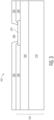
- FIG. 2 illustrates, in a simplified cross-sectional view, the example semiconductor device 100 at a stage of manufacture in accordance with an embodiment.
- the semiconductor device 100 includes a semiconductor die 202.
- the semiconductor die 202 includes a substrate region (e.g., bulk) 210, an active region (e.g., circuitry, interconnect) 206 formed at an active side of the semiconductor die, a bond pad 204 conductively connected to the circuitry and/or interconnect of the active region, and a final passivation layer 208 formed over the active side of the semiconductor die.
- the semiconductor die 202 may be provided in a wafer form or portion of a wafer.
- the semiconductor device 100 may be include an encapsulant (e.g., epoxy molding compound) formed over the backside of the semiconductor die 202.
- the semiconductor die 202 may include any number of conductive interconnect layers and passivation layers.
- the bond pad 204 at a top surface and the overlying final passivation layer 208 are depicted.
- the semiconductor die 202 depicted in FIG. 2 corresponds to the semiconductor die 102 of FIG. 1 .
- the semiconductor die 202 is configured and arranged in an active side up orientation.
- the bond pad 204 at the active side is configured for connection to printed circuit board (PCB) by way of a redistribution layer, SBM structure, and conductive connectors formed at subsequent stages, for example.
- the semiconductor die 202 may be formed from any suitable semiconductor material, such as silicon, germanium, gallium arsenide, gallium nitride, silicon nitride, silicon carbide, and the like.
- the semiconductor die 202 may further include any digital circuits, analog circuits, RF circuits, power circuits, memory, processor, MEMS, sensors, the like, and combinations thereof.
- FIG. 3 illustrates, in a simplified cross-sectional view, the example semiconductor device 100 at a subsequent stage of manufacture in accordance with an embodiment.
- the semiconductor device 100 includes a first non-conductive (e.g., dielectric) layer 302 formed over the semiconductor die 202.
- the non-conductive layer 302 is deposited or otherwise applied on the top surface of the semiconductor die 202.
- the non-conductive layer 302 may be formed from suitable non-conducting polymer materials such as polyimide, PBO, and the like, for example.
- the non-conductive layer 302 is patterned to form an opening 304.
- the opening 304 is located directly over the bond pad 204 such that a substantial portion of the top surface of the bond pad 204 is exposed (e.g., not covered with the non-conductive layer 302).
- FIG. 4 illustrates, in a simplified cross-sectional view, the example semiconductor device 100 at a subsequent stage of manufacture in accordance with an embodiment.
- the semiconductor device 100 includes a metal RDL formed over the non-conductive layer 302 and exposed portion of the bond pad 204.
- the RDL may be formed by way of sputtering or electroplating a metal material (e.g., copper), for example.
- the RDL is patterned to form a plurality of RDL interconnection traces such as the interconnection trace 402 depicted in FIG. 4 .
- the interconnection trace 402 may correspond to the interconnection trace 106 depicted in FIG. 1 , for example.
- interconnection trace 402 includes a first portion 404 directly connected to the top surface of the bond pad 204 and a second portion 406 configured as a base for formation of an SBM structure at a subsequent stage of manufacture.
- the interconnection trace 402 is configured to interconnect the bond pad 204 with the SBM structure formed at a subsequent stage, for example.
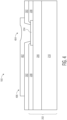
- FIG. 5 illustrates, in a simplified cross-sectional view, the example semiconductor device 100 at a subsequent stage of manufacture in accordance with an embodiment.
- the semiconductor device 100 includes a metal (e.g., copper) SBM structure 502 formed on the exposed portion of the interconnection trace 402.
- the SBM structure includes a plurality of vertical metal wall segments 504 arranged to substantially surround a central opening or cavity 506.
- Each of the vertical metal wall segments 504 is separated from a neighboring vertical metal wall segment by a respective vertical gap (not shown).
- the arrangement of the vertical metal wall segments 504 surrounding the central opening 506 may serve as a socket structure for placement of a ball connector (e.g., solder ball) at a subsequent stage of manufacture, for example.
- a ball connector e.g., solder ball
- the vertical metal wall segments 504 of the SBM structure 502 maybe formed by way of a plating process.
- a seed layer (not shown) may be formed and patterned on an exposed portion of the interconnection trace 402 (e.g., second portion 406 of FIG. 4 ).
- the plurality of vertical metal wall segments 504 of the SBM structure are formed as electroplated copper pillars by utilizing the patterned seed layer, for example.
- the vertical metal wall segments 504 are formed having a substantially uniform height dimension 508 and a (shortest) horizontal width or diameter dimension 510 across the central opening 506. In this embodiment, it is desirable for the height dimension 508 to be approximately in a range of 40-60% of the horizontal width or diameter dimension 510.
- FIG. 6 illustrates, in a simplified cross-sectional view, the example semiconductor device 100 at a subsequent stage of manufacture in accordance with an embodiment.
- the semiconductor device 100 includes a second non-conductive (e.g., dielectric) layer 602 formed over the first non-conductive layer 302 and the exposed portions of the interconnection trace 402.
- the non-conductive layer 602 is deposited or otherwise applied on the top surface of the semiconductor die 202.
- the non-conductive layer 602 is patterned to form an opening through the non-conductive layer 602 such that the central opening 506 is void of the non-conductive layer 602.
- the patterned opening through the non-conductive layer 602 is located directly over the SBM structure 502 such that the portion of the interconnection trace 402 at the bottom of the central opening 506 remains exposed.
- a portion of the non-conductive layer 602 surrounds an outer perimeter of the SBM structure 502.
- FIG. 7 illustrates, in a simplified cross-sectional view, the example semiconductor device 100 at a subsequent stage of manufacture in accordance with an embodiment.
- the semiconductor device 100 includes a ball connector 702 placed into the central opening of the SBM structure 502.
- the plurality of vertical metal wall segments 504 substantially surrounds the ball connector 702.
- the ball connector 702 may be characterized as a solder ball being formed from a solder or solder alloy material.
- the ball connector 702 may be formed as a solder coated spere having a solid metal core (e.g., copper, copper alloy).
- the ball connector 702 is a substantially round sphere having a maximum diameter dimension 704.
- the height dimension 508 of the vertical metal wall segments 504 is desirable for the height dimension 508 of the vertical metal wall segments 504 to be approximately in a range of 40-60% of the maximum diameter dimension 704 the ball connector 702.
- FIG. 8 illustrates, in a simplified cross-sectional view, the example semiconductor device 100 at a subsequent stage of manufacture in accordance with an embodiment.
- the semiconductor device 100 includes a reflowed ball connector 802 (e.g., reflowed solder ball) wetted to the SBM structure 502 and underlying portion of the interconnection trace 402.
- the semiconductor device is subjected to a reflow thermal cycle such that the ball connector 702 depicted in FIG. 7 is reflowed to form the reflowed ball connector 802 depicted in FIG. 8 .
- the ball connector material melts and wets to the inner sidewall surfaces of the SBM structure while venting any potentially trapped air or gases through the vertical gaps located between the vertical metal wall segments 504.
- the ball connector material melts and is wetted to the inner sidewalls of the plurality of vertical metal wall segments 504 and the portion of the trace 402 surrounded by the plurality of vertical metal wall segments 504 exposed at the bottom of the SBM structure 502.
- FIG. 9A through FIG. 9C illustrate, in simplified plan views, example SBM structures of the semiconductor device 100 at a stage of manufacture in accordance with an embodiment.
- Each of the plan views depicted in FIG. 9A through FIG. 9C include a focused portion of the semiconductor device 100 showing example alternative SBM structures for the SBM structure 108 and consistent with the stage of manufacture depicted in FIG. 1 .
- FIG. 9A illustrates, in a simplified plan view, the focused portion of the example semiconductor device 100 with an example SBM structure 902 in accordance with an embodiment.
- the SBM structure 902 includes a plurality of vertical metal wall segments 912 substantially surrounding a central opening 910.
- each of the vertical metal wall segments 912 is formed as a substantially round vertical wall segment.
- the plurality of vertical metal wall segments 912 of the SBM structure 902 may be formed as electroplated copper pillars, for example.
- the plurality of vertical metal wall segments 912 are arranged in a series around an outer perimeter base portion of the interconnection trace 914.
- Each of the vertical metal wall segments 912 is separated from a neighboring vertical metal wall segment by a vertical gap 916.
- the vertical gap is formed having a predetermined lateral width dimension 918 in a range with a minimum value of approximately 10 microns and maximum value chosen such that reflowed ball connector material does not significantly flow past an outer perimeter of the SBM structure 902.
- FIG. 9B illustrates, in a simplified plan view, the focused portion of the example semiconductor device 100 with an example SBM structure 904 in accordance with an embodiment.
- the SBM structure 904 includes a plurality of vertical metal wall segments 922 substantially surrounding a central opening 920.
- each of the vertical metal wall segments 922 is formed as a substantially square or rectilinear vertical wall segment.
- the plurality of vertical metal wall segments 922 of the SBM structure 904 may be formed as electroplated copper pillars, for example.
- the plurality of vertical metal wall segments 922 are arranged in a series around an outer perimeter base portion of the interconnection trace 924.
- Each of the vertical metal wall segments 922 is separated from a neighboring vertical metal wall segment by a vertical gap 926.
- the vertical gap is formed having a predetermined lateral width dimension 928 in a range with a minimum value of approximately 10 microns and maximum value chosen such that reflowed ball connector material does not significantly flow past an outer perimeter of the SBM structure 904.
- FIG. 9C illustrates, in a simplified plan view, the focused portion of the example semiconductor device 100 with an example SBM structure 906 in accordance with an embodiment.
- the SBM structure 906 includes a plurality of vertical metal wall segments 932 substantially surrounding a central opening 930.
- each of the vertical metal wall segments 932 is formed as a substantially oval vertical wall segment.
- the plurality of vertical metal wall segments 932 of the SBM structure 906 may be formed as electroplated copper pillars, for example.
- the plurality of vertical metal wall segments 932 are arranged in a series around an outer perimeter base portion of the interconnection trace 934.
- Each of the vertical metal wall segments 932 is separated from a neighboring vertical metal wall segment by a vertical gap 936.
- the vertical gap is formed having a predetermined lateral width dimension 938 in a range with a minimum value of approximately 10 microns and maximum value chosen such that reflowed ball connector material does not significantly flow past an outer perimeter of the SBM structure 906.
- a method including forming a first non-conductive layer over a top side a semiconductor die; patterning the first non-conductive layer to form an opening exposing a top surface of a bond pad of the semiconductor die; forming a metal trace of a redistribution layer (RDL) over a portion of the first non-conductive layer and exposed top surface of the bond pad; and forming a surrounding bump metallization (SBM) structure on a portion of the metal trace, the SBM structure including a plurality of vertical metal wall segments surrounding a central opening.
- the method may further include placing a ball connector into the central opening of the SBM structure such that the plurality of vertical metal wall segments substantially surround the ball connector.
- a height dimension of the plurality of vertical metal wall segments may be approximately in a range of 40% to 60% of the largest diameter of the ball connector.
- the method may further include reflowing the ball connector such that conductive material of the ball connector wets to the entire inner sidewalls of the plurality of vertical metal wall segments of the SBM.
- the each of the vertical metal wall segments of plurality of vertical metal wall segments may be separated from a neighboring vertical metal wall segment by a respective gap, the gap having a predetermined lateral dimension.
- the predetermined lateral dimension of the gap may be substantially 10 microns or greater.
- the gap may extend vertically from the portion of the metal trace to a top of the plurality of vertical metal wall segments.
- the forming the SBM structure may include forming the plurality of vertical metal wall segments as electroplated copper pillars.
- the method may further include forming a second non-conductive layer over the first non-conductive layer and exposed portions of the metal trace; and patterning the second non-conductive layer such that a top surface of the metal trace is exposed in the central opening of the SBM structure.
- a semiconductor device including a first non-conductive layer over a top side a semiconductor die, an opening in the first non-conductive layer exposes a top surface of a bond pad of the semiconductor die; a metal trace of a redistribution layer formed over a portion of the first non-conductive layer and exposed top surface of the bond pad; and a surrounding bump metallization (SBM) structure formed on a portion of the metal trace, the SBM structure including a plurality of vertical metal wall segments surrounding a central opening.
- the plurality of vertical metal wall segments of the SBM structure may be formed as electroplated copper pillars.
- a height dimension of the plurality of vertical metal wall segments may be substantially in a range of 40% to 60% of a horizontal width or diameter of the central opening.
- the semiconductor device may further include a reflowed ball connector surrounded by the plurality of vertical metal wall segments such that conductive material of the ball connector may be wetted to the inner sidewalls of the plurality of vertical metal wall segments and to the portion of the metal trace.
- a height dimension of the plurality of vertical metal wall segments may be at least 50% of a maximum height dimension of the reflowed ball connector.
- Each vertical metal wall segment of the plurality of vertical metal wall segments may be separated from a neighboring vertical wall segment by way of a gap, the gap having a predetermined lateral dimension.
- a method including forming a first non-conductive layer over a top side a semiconductor die; patterning the first non-conductive layer to form an opening exposing a top surface of a bond pad of the semiconductor die; forming a metal trace of a redistribution layer (RDL) over a portion of the first non-conductive layer and exposed top surface of the bond pad; forming a surrounding bump metallization (SBM) structure on a portion of the metal trace, the SBM structure including a plurality of vertical metal wall segments surrounding a central opening, each vertical metal wall segment separated from a neighboring vertical wall segment by way of a vertical gap; forming a second non-conductive layer over the first non-conductive layer and exposed portions of the metal trace; and patterning the second non-conductive layer such that a top surface of the metal trace is exposed in the central opening of the SBM structure.
- RDL redistribution layer
- the method may further include placing a ball connector into the central opening of the SBM structure such that the plurality of vertical metal wall segments substantially surround the ball connector.
- the method may further include reflowing the ball connector such that conductive material of the ball connector wets to the entire inner sidewalls of the plurality of vertical metal wall segments of the SBM structure and to the portion of the metal trace.
- the vertical gap may be formed having a predetermined lateral dimension, the predetermined lateral dimension substantially 10 microns or greater.
- the plurality of vertical metal wall segments of the SBM structure may be formed as electroplated copper pillars.
- the semiconductor device includes a patterned redistribution layer.
- a plurality of interconnections traces are formed from the patterned redistribution layer.
- Each interconnection trace includes a first portion connected to a top surface of a respective bond pad and a second portion configured as a base for formation of a surrounding bump metallization structure.
- a plurality of surrounding bump metallization structures are formed on respective interconnection traces.
- Each of surrounding bump metallization structure includes a plurality of vertical metal wall segments formed around an outer perimeter region of the second portion of the interconnection trace.
- a central opening or cavity is formed by the surrounding plurality of the vertical metal wall segments.
- Each of the vertical metal wall segments is separated from a neighboring vertical metal wall segment by a vertical gap.
- Each of the surrounding bump metallization structures is configured to serve as a socket for receiving a ball connector.
- the vertical gap allows air to vent as the ball connector material is melted.
- the width of the gap is chosen such that it is large enough for air to escape and small enough to keep the melted ball connector material from oozing out of the socket.
Landscapes
- Internal Circuitry In Semiconductor Integrated Circuit Devices (AREA)
- Physics & Mathematics (AREA)
- Geometry (AREA)
Abstract
Description
- This disclosure relates generally to semiconductor device packaging, and more specifically, to a semiconductor device with a surrounding bump metallization and method of forming the same.
- Today, there is an increasing trend to include sophisticated semiconductor devices in products and systems that are used every day. These sophisticated semiconductor devices may include features for specific applications which may impact the configuration of the semiconductor device packages, for example. For some features and applications, the configuration of the semiconductor device packages may be susceptible to lower reliability, lower performance, and higher product or system costs. Accordingly, significant challenges exist in accommodating these features and applications while minimizing the impact on semiconductor devices' reliability, performance, and costs.
- The present invention is illustrated by way of example and is not limited by the accompanying figures, in which like references indicate similar elements. Elements in the figures are illustrated for simplicity and clarity and have not necessarily been drawn to scale.
-
FIG. 1 illustrates, in a simplified plan view, an example semiconductor device having a surrounding bump metallization structure in accordance with an embodiment. -
FIG. 2 through FIG. 8 illustrate, in simplified cross-sectional views, the example semiconductor device taken along line A-A ofFIG. 1 at various stages of manufacture in accordance with an embodiment. -
FIG. 9A through FIG. 9C illustrate, in simplified plan views, example surrounding bump metallization structures of the semiconductor device in accordance with an embodiment. - Generally, there is provided, a semiconductor device with a surrounding bump metallization. The semiconductor device includes a patterned redistribution layer. A plurality of interconnections traces are formed from the patterned redistribution layer. Each interconnection trace includes a first portion connected to a top surface of a respective bond pad and a second portion configured as a base for formation of a surrounding bump metallization structure. A plurality of surrounding bump metallization structures are formed on respective interconnection traces. Each of surrounding bump metallization structure includes a plurality of vertical metal wall segments formed around an outer perimeter region of the second portion of the interconnection trace. A central opening or cavity is formed by the surrounding plurality of the vertical metal wall segments. Each of the vertical metal wall segments is separated from a neighboring vertical metal wall segment by a vertical gap. Each of the surrounding bump metallization structures is configured to serve as a socket for receiving a ball connector. The vertical gap allows air to vent as the ball connector material is melted. The width of the gap is chosen such that it is large enough for air to escape and small enough to keep the melted ball connector material from oozing out of the socket. By forming the surrounding bump metallization structures in this manner, the ball connections with semiconductor device are more robust and provide superior reliability along with tighter ball pitch control.
-
FIG. 1 illustrates, in a simplified plan view, a portion of anexample semiconductor device 100 having a surrounding bump metallization (SBM) structure in accordance with an embodiment. Thedevice 100 includes a semiconductor die 102,bond pads 104 formed at the top side of the semiconductor die, conductive (e.g., metal) interconnections traces 106 of a patterned redistribution layer (RDL) formed over the semiconductor die 102, and a plurality ofSBM structures 108 formed onrespective traces 106. The term "conductive," as used herein, generally refers to electrical conductivity unless otherwise described. In this embodiment, each of theinterconnections traces 106 includes a first portion directly connected to a top surface of arespective bond pad 104 and a second portion configured as a base for formation of aSBM structure 108. - In this embodiment, the SBM structure includes a plurality of vertical
metal wall segments 110 formed around an outer perimeter region of the second portion of thetrace 106. The verticalmetal wall segments 110 are arranged to substantially surround a central opening orcavity 114. Each of the verticalmetal wall segments 110 is separated from a neighboring vertical metal wall segment by a respectivevertical gap 112. The arrangement of the verticalmetal wall segments 110 surrounding thecentral opening 114 may be characterized as a socket structure configured to receive a ball connector (e.g., solder ball) at a subsequent stage of manufacture, for example. Thevertical gap 112 is therefore configured to have a predetermined width such that the gap width is large enough to vent air/gas when the ball connector is reflowed yet small enough to prevent reflowed material from extending significantly beyond an outer perimeter formed by the plurality of verticalmetal wall segments 110. - The number, shape, and arrangement of the vertical
metal wall segments 110 andRDL interconnection traces 106 are chosen for illustration purposes. Some features of thesemiconductor device 100 such as intermediate layers disposed between thesemiconductor die 102 and the RDL are not shown for illustration purposes. Even though the embodiment ofFIG. 1 is depicted in a "fan-in" configuration, embodiments in other configurations (e.g., "fan-out") are anticipated by this disclosure. Cross-sectional views of theexample semiconductor device 100 taken along line A-A ofFIG. 1 at stages of manufacture are depicted inFIG. 2 through FIG. 8 . -
FIG. 2 illustrates, in a simplified cross-sectional view, theexample semiconductor device 100 at a stage of manufacture in accordance with an embodiment. At this stage of manufacture, thesemiconductor device 100 includes asemiconductor die 202. In this embodiment, the semiconductor die 202 includes a substrate region (e.g., bulk) 210, an active region (e.g., circuitry, interconnect) 206 formed at an active side of the semiconductor die, abond pad 204 conductively connected to the circuitry and/or interconnect of the active region, and afinal passivation layer 208 formed over the active side of the semiconductor die. In some embodiments, the semiconductor die 202 may be provided in a wafer form or portion of a wafer. In some embodiments (e.g., wafer-level chip-scale packaging), thesemiconductor device 100 may be include an encapsulant (e.g., epoxy molding compound) formed over the backside of thesemiconductor die 202. The semiconductor die 202 may include any number of conductive interconnect layers and passivation layers. For illustration purposes, thebond pad 204 at a top surface and the overlyingfinal passivation layer 208 are depicted. In this embodiment, the semiconductor die 202 depicted inFIG. 2 corresponds to the semiconductor die 102 ofFIG. 1 . - The semiconductor die 202 is configured and arranged in an active side up orientation. The
bond pad 204 at the active side is configured for connection to printed circuit board (PCB) by way of a redistribution layer, SBM structure, and conductive connectors formed at subsequent stages, for example. The semiconductor die 202 may be formed from any suitable semiconductor material, such as silicon, germanium, gallium arsenide, gallium nitride, silicon nitride, silicon carbide, and the like. The semiconductor die 202 may further include any digital circuits, analog circuits, RF circuits, power circuits, memory, processor, MEMS, sensors, the like, and combinations thereof. -
FIG. 3 illustrates, in a simplified cross-sectional view, theexample semiconductor device 100 at a subsequent stage of manufacture in accordance with an embodiment. At this stage of manufacture, thesemiconductor device 100 includes a first non-conductive (e.g., dielectric)layer 302 formed over thesemiconductor die 202. Thenon-conductive layer 302 is deposited or otherwise applied on the top surface of thesemiconductor die 202. Thenon-conductive layer 302 may be formed from suitable non-conducting polymer materials such as polyimide, PBO, and the like, for example. In this embodiment, thenon-conductive layer 302 is patterned to form anopening 304. The opening 304 is located directly over thebond pad 204 such that a substantial portion of the top surface of thebond pad 204 is exposed (e.g., not covered with the non-conductive layer 302). -
FIG. 4 illustrates, in a simplified cross-sectional view, theexample semiconductor device 100 at a subsequent stage of manufacture in accordance with an embodiment. At this stage of manufacture, thesemiconductor device 100 includes a metal RDL formed over thenon-conductive layer 302 and exposed portion of thebond pad 204. The RDL may be formed by way of sputtering or electroplating a metal material (e.g., copper), for example. In this embodiment, the RDL is patterned to form a plurality of RDL interconnection traces such as theinterconnection trace 402 depicted inFIG. 4 . Theinterconnection trace 402 may correspond to theinterconnection trace 106 depicted inFIG. 1 , for example. In this embodiment,interconnection trace 402 includes afirst portion 404 directly connected to the top surface of thebond pad 204 and asecond portion 406 configured as a base for formation of an SBM structure at a subsequent stage of manufacture. Theinterconnection trace 402 is configured to interconnect thebond pad 204 with the SBM structure formed at a subsequent stage, for example. -
FIG. 5 illustrates, in a simplified cross-sectional view, theexample semiconductor device 100 at a subsequent stage of manufacture in accordance with an embodiment. At this stage of manufacture, thesemiconductor device 100 includes a metal (e.g., copper)SBM structure 502 formed on the exposed portion of theinterconnection trace 402. In this embodiment, the SBM structure includes a plurality of verticalmetal wall segments 504 arranged to substantially surround a central opening orcavity 506. Each of the verticalmetal wall segments 504 is separated from a neighboring vertical metal wall segment by a respective vertical gap (not shown). The arrangement of the verticalmetal wall segments 504 surrounding thecentral opening 506 may serve as a socket structure for placement of a ball connector (e.g., solder ball) at a subsequent stage of manufacture, for example. In this embodiment, the verticalmetal wall segments 504 of theSBM structure 502 maybe formed by way of a plating process. For example, a seed layer (not shown) may be formed and patterned on an exposed portion of the interconnection trace 402 (e.g.,second portion 406 ofFIG. 4 ). The plurality of verticalmetal wall segments 504 of the SBM structure are formed as electroplated copper pillars by utilizing the patterned seed layer, for example. In this embodiment, the verticalmetal wall segments 504 are formed having a substantiallyuniform height dimension 508 and a (shortest) horizontal width ordiameter dimension 510 across thecentral opening 506. In this embodiment, it is desirable for theheight dimension 508 to be approximately in a range of 40-60% of the horizontal width ordiameter dimension 510. -
FIG. 6 illustrates, in a simplified cross-sectional view, theexample semiconductor device 100 at a subsequent stage of manufacture in accordance with an embodiment. At this stage of manufacture, thesemiconductor device 100 includes a second non-conductive (e.g., dielectric)layer 602 formed over the firstnon-conductive layer 302 and the exposed portions of theinterconnection trace 402. Thenon-conductive layer 602 is deposited or otherwise applied on the top surface of the semiconductor die 202. Thenon-conductive layer 602 is patterned to form an opening through thenon-conductive layer 602 such that thecentral opening 506 is void of thenon-conductive layer 602. The patterned opening through thenon-conductive layer 602 is located directly over theSBM structure 502 such that the portion of theinterconnection trace 402 at the bottom of thecentral opening 506 remains exposed. In this embodiment, a portion of thenon-conductive layer 602 surrounds an outer perimeter of theSBM structure 502. -
FIG. 7 illustrates, in a simplified cross-sectional view, theexample semiconductor device 100 at a subsequent stage of manufacture in accordance with an embodiment. At this stage of manufacture, thesemiconductor device 100 includes aball connector 702 placed into the central opening of theSBM structure 502. When placed into the SBM structure, the plurality of verticalmetal wall segments 504 substantially surrounds theball connector 702. In this embodiment, theball connector 702 may be characterized as a solder ball being formed from a solder or solder alloy material. In some embodiments, theball connector 702 may be formed as a solder coated spere having a solid metal core (e.g., copper, copper alloy). In this embodiment, theball connector 702 is a substantially round sphere having amaximum diameter dimension 704. In this embodiment, it is desirable for theheight dimension 508 of the verticalmetal wall segments 504 to be approximately in a range of 40-60% of themaximum diameter dimension 704 theball connector 702. By keeping the vertical metal wallsegments height dimension 508 roughly half of the ballconnector diameter dimension 704, an ample dome of ball connector material will remain above the top of the verticalmetal wall segments 504 after reflowing at a subsequent stage. -
FIG. 8 illustrates, in a simplified cross-sectional view, theexample semiconductor device 100 at a subsequent stage of manufacture in accordance with an embodiment. At this stage of manufacture, thesemiconductor device 100 includes a reflowed ball connector 802 (e.g., reflowed solder ball) wetted to theSBM structure 502 and underlying portion of theinterconnection trace 402. In this embodiment, the semiconductor device is subjected to a reflow thermal cycle such that theball connector 702 depicted inFIG. 7 is reflowed to form the reflowedball connector 802 depicted inFIG. 8 . During the reflow thermal cycle, the ball connector material melts and wets to the inner sidewall surfaces of the SBM structure while venting any potentially trapped air or gases through the vertical gaps located between the verticalmetal wall segments 504. In this embodiment, the ball connector material melts and is wetted to the inner sidewalls of the plurality of verticalmetal wall segments 504 and the portion of thetrace 402 surrounded by the plurality of verticalmetal wall segments 504 exposed at the bottom of theSBM structure 502. By reflowing theball connector 802 in this manner, a robust and reliable joint and connection with theSBM structure 502 is formed without voids. -
FIG. 9A through FIG. 9C illustrate, in simplified plan views, example SBM structures of thesemiconductor device 100 at a stage of manufacture in accordance with an embodiment. Each of the plan views depicted inFIG. 9A through FIG. 9C include a focused portion of thesemiconductor device 100 showing example alternative SBM structures for theSBM structure 108 and consistent with the stage of manufacture depicted inFIG. 1 . -
FIG. 9A illustrates, in a simplified plan view, the focused portion of theexample semiconductor device 100 with anexample SBM structure 902 in accordance with an embodiment. In this embodiment, theSBM structure 902 includes a plurality of verticalmetal wall segments 912 substantially surrounding acentral opening 910. In this embodiment, each of the verticalmetal wall segments 912 is formed as a substantially round vertical wall segment. The plurality of verticalmetal wall segments 912 of theSBM structure 902 may be formed as electroplated copper pillars, for example. The plurality of verticalmetal wall segments 912 are arranged in a series around an outer perimeter base portion of theinterconnection trace 914. Each of the verticalmetal wall segments 912 is separated from a neighboring vertical metal wall segment by avertical gap 916. In this embodiment, the vertical gap is formed having a predeterminedlateral width dimension 918 in a range with a minimum value of approximately 10 microns and maximum value chosen such that reflowed ball connector material does not significantly flow past an outer perimeter of theSBM structure 902. -
FIG. 9B illustrates, in a simplified plan view, the focused portion of theexample semiconductor device 100 with anexample SBM structure 904 in accordance with an embodiment. In this embodiment, theSBM structure 904 includes a plurality of verticalmetal wall segments 922 substantially surrounding acentral opening 920. In this embodiment, each of the verticalmetal wall segments 922 is formed as a substantially square or rectilinear vertical wall segment. The plurality of verticalmetal wall segments 922 of theSBM structure 904 may be formed as electroplated copper pillars, for example. The plurality of verticalmetal wall segments 922 are arranged in a series around an outer perimeter base portion of theinterconnection trace 924. Each of the verticalmetal wall segments 922 is separated from a neighboring vertical metal wall segment by avertical gap 926. In this embodiment, the vertical gap is formed having a predeterminedlateral width dimension 928 in a range with a minimum value of approximately 10 microns and maximum value chosen such that reflowed ball connector material does not significantly flow past an outer perimeter of theSBM structure 904. -
FIG. 9C illustrates, in a simplified plan view, the focused portion of theexample semiconductor device 100 with anexample SBM structure 906 in accordance with an embodiment. In this embodiment, theSBM structure 906 includes a plurality of verticalmetal wall segments 932 substantially surrounding acentral opening 930. In this embodiment, each of the verticalmetal wall segments 932 is formed as a substantially oval vertical wall segment. The plurality of verticalmetal wall segments 932 of theSBM structure 906 may be formed as electroplated copper pillars, for example. The plurality of verticalmetal wall segments 932 are arranged in a series around an outer perimeter base portion of theinterconnection trace 934. Each of the verticalmetal wall segments 932 is separated from a neighboring vertical metal wall segment by avertical gap 936. In this embodiment, the vertical gap is formed having a predeterminedlateral width dimension 938 in a range with a minimum value of approximately 10 microns and maximum value chosen such that reflowed ball connector material does not significantly flow past an outer perimeter of theSBM structure 906. - Generally, there is provided, a method including forming a first non-conductive layer over a top side a semiconductor die; patterning the first non-conductive layer to form an opening exposing a top surface of a bond pad of the semiconductor die; forming a metal trace of a redistribution layer (RDL) over a portion of the first non-conductive layer and exposed top surface of the bond pad; and forming a surrounding bump metallization (SBM) structure on a portion of the metal trace, the SBM structure including a plurality of vertical metal wall segments surrounding a central opening. The method may further include placing a ball connector into the central opening of the SBM structure such that the plurality of vertical metal wall segments substantially surround the ball connector. A height dimension of the plurality of vertical metal wall segments may be approximately in a range of 40% to 60% of the largest diameter of the ball connector. The method may further include reflowing the ball connector such that conductive material of the ball connector wets to the entire inner sidewalls of the plurality of vertical metal wall segments of the SBM. The each of the vertical metal wall segments of plurality of vertical metal wall segments may be separated from a neighboring vertical metal wall segment by a respective gap, the gap having a predetermined lateral dimension. The predetermined lateral dimension of the gap may be substantially 10 microns or greater. The gap may extend vertically from the portion of the metal trace to a top of the plurality of vertical metal wall segments. The forming the SBM structure may include forming the plurality of vertical metal wall segments as electroplated copper pillars. The method may further include forming a second non-conductive layer over the first non-conductive layer and exposed portions of the metal trace; and patterning the second non-conductive layer such that a top surface of the metal trace is exposed in the central opening of the SBM structure.
- In another embodiment, there is provided, a semiconductor device including a first non-conductive layer over a top side a semiconductor die, an opening in the first non-conductive layer exposes a top surface of a bond pad of the semiconductor die; a metal trace of a redistribution layer formed over a portion of the first non-conductive layer and exposed top surface of the bond pad; and a surrounding bump metallization (SBM) structure formed on a portion of the metal trace, the SBM structure including a plurality of vertical metal wall segments surrounding a central opening. The plurality of vertical metal wall segments of the SBM structure may be formed as electroplated copper pillars. A height dimension of the plurality of vertical metal wall segments may be substantially in a range of 40% to 60% of a horizontal width or diameter of the central opening. The semiconductor device may further include a reflowed ball connector surrounded by the plurality of vertical metal wall segments such that conductive material of the ball connector may be wetted to the inner sidewalls of the plurality of vertical metal wall segments and to the portion of the metal trace. A height dimension of the plurality of vertical metal wall segments may be at least 50% of a maximum height dimension of the reflowed ball connector. Each vertical metal wall segment of the plurality of vertical metal wall segments may be separated from a neighboring vertical wall segment by way of a gap, the gap having a predetermined lateral dimension.
- In yet another embodiment, there is provided, a method including forming a first non-conductive layer over a top side a semiconductor die; patterning the first non-conductive layer to form an opening exposing a top surface of a bond pad of the semiconductor die; forming a metal trace of a redistribution layer (RDL) over a portion of the first non-conductive layer and exposed top surface of the bond pad; forming a surrounding bump metallization (SBM) structure on a portion of the metal trace, the SBM structure including a plurality of vertical metal wall segments surrounding a central opening, each vertical metal wall segment separated from a neighboring vertical wall segment by way of a vertical gap; forming a second non-conductive layer over the first non-conductive layer and exposed portions of the metal trace; and patterning the second non-conductive layer such that a top surface of the metal trace is exposed in the central opening of the SBM structure. The method may further include placing a ball connector into the central opening of the SBM structure such that the plurality of vertical metal wall segments substantially surround the ball connector. The method may further include reflowing the ball connector such that conductive material of the ball connector wets to the entire inner sidewalls of the plurality of vertical metal wall segments of the SBM structure and to the portion of the metal trace. The vertical gap may be formed having a predetermined lateral dimension, the predetermined lateral dimension substantially 10 microns or greater. The plurality of vertical metal wall segments of the SBM structure may be formed as electroplated copper pillars.
- By now, it should be appreciated that there has been provided a semiconductor device with a surrounding bump metallization. The semiconductor device includes a patterned redistribution layer. A plurality of interconnections traces are formed from the patterned redistribution layer. Each interconnection trace includes a first portion connected to a top surface of a respective bond pad and a second portion configured as a base for formation of a surrounding bump metallization structure. A plurality of surrounding bump metallization structures are formed on respective interconnection traces. Each of surrounding bump metallization structure includes a plurality of vertical metal wall segments formed around an outer perimeter region of the second portion of the interconnection trace. A central opening or cavity is formed by the surrounding plurality of the vertical metal wall segments. Each of the vertical metal wall segments is separated from a neighboring vertical metal wall segment by a vertical gap. Each of the surrounding bump metallization structures is configured to serve as a socket for receiving a ball connector. The vertical gap allows air to vent as the ball connector material is melted. The width of the gap is chosen such that it is large enough for air to escape and small enough to keep the melted ball connector material from oozing out of the socket. By forming the surrounding bump metallization structures in this manner, the ball connections with semiconductor device are more robust and provide superior reliability along with tighter ball pitch control.
- The terms "front," "back," "top," "bottom," "over," "under" and the like in the description and in the claims, if any, are used for descriptive purposes and not necessarily for describing permanent relative positions. It is understood that the terms so used are interchangeable under appropriate circumstances such that the embodiments of the invention described herein are, for example, capable of operation in other orientations than those illustrated or otherwise described herein.
- Although the invention is described herein with reference to specific embodiments, various modifications and changes can be made without departing from the scope of the present invention as set forth in the claims below. Accordingly, the specification and figures are to be regarded in an illustrative rather than a restrictive sense, and all such modifications are intended to be included within the scope of the present invention. Any benefits, advantages, or solutions to problems that are described herein with regard to specific embodiments are not intended to be construed as a critical, required, or essential feature or element of any or all the claims.
- Furthermore, the terms "a" or "an," as used herein, are defined as one or more than one. Also, the use of introductory phrases such as "at least one" and "one or more" in the claims should not be construed to imply that the introduction of another claim element by the indefinite articles "a" or "an" limits any particular claim containing such introduced claim element to inventions containing only one such element, even when the same claim includes the introductory phrases "one or more" or "at least one" and indefinite articles such as "a" or "an." The same holds true for the use of definite articles.
- Unless stated otherwise, terms such as "first" and "second" are used to arbitrarily distinguish between the elements such terms describe. Thus, these terms are not necessarily intended to indicate temporal or other prioritization of such elements.
Claims (15)
- A method comprising:forming a first non-conductive layer over a top side a semiconductor die;patterning the first non-conductive layer to form an opening exposing a top surface of a bond pad of the semiconductor die;forming a metal trace of a redistribution layer, RDL, over a portion of the first non-conductive layer and exposed top surface of the bond pad; andforming a surrounding bump metallization, SBM, structure on a portion of the metal trace, the SBM structure including a plurality of vertical metal wall segments surrounding a central opening.
- The method of claim 1, further comprising placing a ball connector into the central opening of the SBM structure such that the plurality of vertical metal wall segments substantially surround the ball connector.
- The method of claim 2, wherein a height dimension of the plurality of vertical metal wall segments is approximately in a range of 40% to 60% of a largest diameter of the ball connector.
- The method of claim 2 or 3, further comprising reflowing the ball connector such that conductive material of the ball connector wets to the entire inner sidewalls of the plurality of vertical metal wall segments of the SBM.
- The method of any preceding claim, wherein the each of the vertical metal wall segments of plurality of vertical metal wall segments is separated from a neighboring vertical metal wall segment by a respective gap, the gap having a predetermined lateral dimension.
- The method of claim 5, wherein the predetermined lateral dimension of the gap is substantially 10 microns or greater.
- The method of claim 5 or 6, wherein the gap extends vertically from the portion of the metal trace to a top of the plurality of vertical metal wall segments.
- The method of any preceding claim, wherein forming the SBM structure includes forming the plurality of vertical metal wall segments as electroplated copper pillars.
- The method of any preceding claim, further comprising:forming a second non-conductive layer over the first non-conductive layer and exposed portions of the metal trace; andpatterning the second non-conductive layer such that a top surface of the metal trace is exposed in the central opening of the SBM structure.
- A semiconductor device comprising:a first non-conductive layer over a top side a semiconductor die, an opening in the first non-conductive layer exposes a top surface of a bond pad of the semiconductor die;a metal trace of a redistribution layer formed over a portion of the first non-conductive layer and exposed top surface of the bond pad; anda surrounding bump metallization, SBM, structure formed on a portion of the metal trace, the SBM structure including a plurality of vertical metal wall segments surrounding a central opening.
- The semiconductor device of claim 10, wherein the plurality of vertical metal wall segments of the SBM structure are formed as electroplated copper pillars.
- The semiconductor device of claim 10 or 11, wherein a height dimension of the plurality of vertical metal wall segments is substantially in a range of 40% to 60% of a horizontal width or diameter of the central opening.
- The semiconductor device of any of claims 10 to 12, further comprising a reflowed ball connector surrounded by the plurality of vertical metal wall segments such that conductive material of the ball connector is wetted to the inner sidewalls of the plurality of vertical metal wall segments and to the portion of the metal trace.
- The semiconductor device of claim 13, wherein a height dimension of the plurality of vertical metal wall segments is at least 50% of a maximum height dimension of the reflowed ball connector.
- The semiconductor device of any of claims 10 to 14, wherein each vertical metal wall segment of the plurality of vertical metal wall segments is separated from a neighboring vertical wall segment by way of a gap, the gap having a predetermined lateral dimension.
Applications Claiming Priority (1)
| Application Number | Priority Date | Filing Date | Title |
|---|---|---|---|
| US18/489,173 US20250132235A1 (en) | 2023-10-18 | 2023-10-18 | Semiconductor device with surrounding bump metallization and method therefor |
Publications (1)
| Publication Number | Publication Date |
|---|---|
| EP4542644A1 true EP4542644A1 (en) | 2025-04-23 |
Family
ID=93014044
Family Applications (1)
| Application Number | Title | Priority Date | Filing Date |
|---|---|---|---|
| EP24204783.5A Pending EP4542644A1 (en) | 2023-10-18 | 2024-10-04 | Semiconductor device with surrounding bump metallization and method therefor |
Country Status (2)
| Country | Link |
|---|---|
| US (1) | US20250132235A1 (en) |
| EP (1) | EP4542644A1 (en) |
Citations (2)
| Publication number | Priority date | Publication date | Assignee | Title |
|---|---|---|---|---|
| JP4693855B2 (en) * | 2008-03-06 | 2011-06-01 | 株式会社フジクラ | Semiconductor package and manufacturing method thereof |
| US20190148317A1 (en) * | 2017-11-14 | 2019-05-16 | Taiwan Semiconductor Manufacturing Co., Ltd. | Package structure with protrusion structure |
Family Cites Families (5)
| Publication number | Priority date | Publication date | Assignee | Title |
|---|---|---|---|---|
| KR100386081B1 (en) * | 2000-01-05 | 2003-06-09 | 주식회사 하이닉스반도체 | Semiconductor package and fabricating method thereof |
| US20110186989A1 (en) * | 2010-02-04 | 2011-08-04 | Taiwan Semiconductor Manufacturing Company, Ltd. | Semiconductor Device and Bump Formation Process |
| US9418947B2 (en) * | 2012-02-27 | 2016-08-16 | Taiwan Semiconductor Manufacturing Company, Ltd. | Mechanisms for forming connectors with a molding compound for package on package |
| US9362243B2 (en) * | 2014-05-21 | 2016-06-07 | Taiwan Semiconductor Manufacturing Company Ltd. | Semiconductor package device and forming the same |
| KR20190036776A (en) * | 2017-09-28 | 2019-04-05 | 삼성전자주식회사 | Bump structure, semiconductor package including the bump structure, and method of forming the bump structure |
-
2023
- 2023-10-18 US US18/489,173 patent/US20250132235A1/en active Pending
-
2024
- 2024-10-04 EP EP24204783.5A patent/EP4542644A1/en active Pending
Patent Citations (2)
| Publication number | Priority date | Publication date | Assignee | Title |
|---|---|---|---|---|
| JP4693855B2 (en) * | 2008-03-06 | 2011-06-01 | 株式会社フジクラ | Semiconductor package and manufacturing method thereof |
| US20190148317A1 (en) * | 2017-11-14 | 2019-05-16 | Taiwan Semiconductor Manufacturing Co., Ltd. | Package structure with protrusion structure |
Also Published As
| Publication number | Publication date |
|---|---|
| US20250132235A1 (en) | 2025-04-24 |
Similar Documents
| Publication | Publication Date | Title |
|---|---|---|
| US11961742B2 (en) | Semiconductor device and manufacturing method thereof | |
| US9899286B2 (en) | Semiconductor device and method of self-confinement of conductive bump material during reflow without solder mask | |
| EP3031080B1 (en) | Embedded packaging with preformed vias | |
| US9345148B2 (en) | Semiconductor device and method of forming flipchip interconnection structure with bump on partial pad | |
| US9679811B2 (en) | Semiconductor device and method of confining conductive bump material with solder mask patch | |
| TWI541916B (en) | Semiconductor device and method for forming a flip chip interconnect structure | |
| US8643164B2 (en) | Package-on-package technology for fan-out wafer-level packaging | |
| US20160043041A1 (en) | Semiconductor packages and methods of packaging semiconductor devices | |
| US20130075900A1 (en) | Semiconductor Device and Method of Forming Insulating Layer on Conductive Traces for Electrical Isolation in Fine Pitch Bonding | |
| US20080230925A1 (en) | Solder-bumping structures produced by a solder bumping method | |
| KR20090071365A (en) | Semiconductor device manufacturing method using semiconductor device and sacrificial carrier | |
| CN102487021A (en) | Semiconductor device and method of forming pad layout for flipchip semiconductor die | |
| US12469759B2 (en) | Semiconductor package | |
| US9324681B2 (en) | Pin attachment | |
| US10804114B2 (en) | Methods for making a multilevel leadframe by etching a conductive sheet from two opposite sides | |
| US20250155105A1 (en) | Semiconductor device and manufacturing method thereof | |
| US9159682B2 (en) | Copper pillar bump and flip chip package using same | |
| US6664176B2 (en) | Method of making pad-rerouting for integrated circuit chips | |
| CN114883196A (en) | Semiconductor device and method for manufacturing the same | |
| US7045893B1 (en) | Semiconductor package and method for manufacturing the same | |
| US20080315394A1 (en) | Semiconductor package and a method for manufacturing the same | |
| US20250132235A1 (en) | Semiconductor device with surrounding bump metallization and method therefor | |
| US20240105659A1 (en) | Semiconductor device with redistribution metallization and method therefor | |
| EP4498408A1 (en) | Semiconductor device with redistribution layer and method therefor |
Legal Events
| Date | Code | Title | Description |
|---|---|---|---|
| PUAI | Public reference made under article 153(3) epc to a published international application that has entered the european phase |
Free format text: ORIGINAL CODE: 0009012 |
|
| STAA | Information on the status of an ep patent application or granted ep patent |
Free format text: STATUS: THE APPLICATION HAS BEEN PUBLISHED |
|
| AK | Designated contracting states |
Kind code of ref document: A1 Designated state(s): AL AT BE BG CH CY CZ DE DK EE ES FI FR GB GR HR HU IE IS IT LI LT LU LV MC ME MK MT NL NO PL PT RO RS SE SI SK SM TR |
|
| STAA | Information on the status of an ep patent application or granted ep patent |
Free format text: STATUS: REQUEST FOR EXAMINATION WAS MADE |
|
| 17P | Request for examination filed |
Effective date: 20251023 |
|
| REG | Reference to a national code |
Ref country code: DE Ref legal event code: R079 Free format text: PREVIOUS MAIN CLASS: H01L0023485000 Ipc: H10W0072200000 |
|
| RIC1 | Information provided on ipc code assigned before grant |
Ipc: H10W 72/20 20260101AFI20260408BHEP Ipc: H10W 70/65 20260101ALN20260408BHEP Ipc: H10W 72/00 20260101ALN20260408BHEP Ipc: H10W 72/29 20260101ALN20260408BHEP Ipc: H10W 72/90 20260101ALN20260408BHEP |