EP4542627A1 - Substrate processing method and substrate processing system - Google Patents
Substrate processing method and substrate processing system Download PDFInfo
- Publication number
- EP4542627A1 EP4542627A1 EP23823704.4A EP23823704A EP4542627A1 EP 4542627 A1 EP4542627 A1 EP 4542627A1 EP 23823704 A EP23823704 A EP 23823704A EP 4542627 A1 EP4542627 A1 EP 4542627A1
- Authority
- EP
- European Patent Office
- Prior art keywords
- film
- metal oxide
- gas
- substrate
- resist film
- Prior art date
- Legal status (The legal status is an assumption and is not a legal conclusion. Google has not performed a legal analysis and makes no representation as to the accuracy of the status listed.)
- Pending
Links
Images








Classifications
-
- C—CHEMISTRY; METALLURGY
- C23—COATING METALLIC MATERIAL; COATING MATERIAL WITH METALLIC MATERIAL; CHEMICAL SURFACE TREATMENT; DIFFUSION TREATMENT OF METALLIC MATERIAL; COATING BY VACUUM EVAPORATION, BY SPUTTERING, BY ION IMPLANTATION OR BY CHEMICAL VAPOUR DEPOSITION, IN GENERAL; INHIBITING CORROSION OF METALLIC MATERIAL OR INCRUSTATION IN GENERAL
- C23C—COATING METALLIC MATERIAL; COATING MATERIAL WITH METALLIC MATERIAL; SURFACE TREATMENT OF METALLIC MATERIAL BY DIFFUSION INTO THE SURFACE, BY CHEMICAL CONVERSION OR SUBSTITUTION; COATING BY VACUUM EVAPORATION, BY SPUTTERING, BY ION IMPLANTATION OR BY CHEMICAL VAPOUR DEPOSITION, IN GENERAL
- C23C16/00—Chemical coating by decomposition of gaseous compounds, without leaving reaction products of surface material in the coating, i.e. chemical vapour deposition [CVD] processes
- C23C16/22—Chemical coating by decomposition of gaseous compounds, without leaving reaction products of surface material in the coating, i.e. chemical vapour deposition [CVD] processes characterised by the deposition of inorganic material, other than metallic material
- C23C16/30—Deposition of compounds, mixtures or solid solutions, e.g. borides, carbides, nitrides
- C23C16/40—Oxides
-
- C—CHEMISTRY; METALLURGY
- C23—COATING METALLIC MATERIAL; COATING MATERIAL WITH METALLIC MATERIAL; CHEMICAL SURFACE TREATMENT; DIFFUSION TREATMENT OF METALLIC MATERIAL; COATING BY VACUUM EVAPORATION, BY SPUTTERING, BY ION IMPLANTATION OR BY CHEMICAL VAPOUR DEPOSITION, IN GENERAL; INHIBITING CORROSION OF METALLIC MATERIAL OR INCRUSTATION IN GENERAL
- C23C—COATING METALLIC MATERIAL; COATING MATERIAL WITH METALLIC MATERIAL; SURFACE TREATMENT OF METALLIC MATERIAL BY DIFFUSION INTO THE SURFACE, BY CHEMICAL CONVERSION OR SUBSTITUTION; COATING BY VACUUM EVAPORATION, BY SPUTTERING, BY ION IMPLANTATION OR BY CHEMICAL VAPOUR DEPOSITION, IN GENERAL
- C23C16/00—Chemical coating by decomposition of gaseous compounds, without leaving reaction products of surface material in the coating, i.e. chemical vapour deposition [CVD] processes
- C23C16/56—After-treatment
-
- G—PHYSICS
- G03—PHOTOGRAPHY; CINEMATOGRAPHY; ANALOGOUS TECHNIQUES USING WAVES OTHER THAN OPTICAL WAVES; ELECTROGRAPHY; HOLOGRAPHY
- G03F—PHOTOMECHANICAL PRODUCTION OF TEXTURED OR PATTERNED SURFACES, e.g. FOR PRINTING, FOR PROCESSING OF SEMICONDUCTOR DEVICES; MATERIALS THEREFOR; ORIGINALS THEREFOR; APPARATUS SPECIALLY ADAPTED THEREFOR
- G03F7/00—Photomechanical, e.g. photolithographic, production of textured or patterned surfaces, e.g. printing surfaces; Materials therefor, e.g. comprising photoresists; Apparatus specially adapted therefor
- G03F7/004—Photosensitive materials
- G03F7/0042—Photosensitive materials with inorganic or organometallic light-sensitive compounds not otherwise provided for, e.g. inorganic resists
-
- G—PHYSICS
- G03—PHOTOGRAPHY; CINEMATOGRAPHY; ANALOGOUS TECHNIQUES USING WAVES OTHER THAN OPTICAL WAVES; ELECTROGRAPHY; HOLOGRAPHY
- G03F—PHOTOMECHANICAL PRODUCTION OF TEXTURED OR PATTERNED SURFACES, e.g. FOR PRINTING, FOR PROCESSING OF SEMICONDUCTOR DEVICES; MATERIALS THEREFOR; ORIGINALS THEREFOR; APPARATUS SPECIALLY ADAPTED THEREFOR
- G03F7/00—Photomechanical, e.g. photolithographic, production of textured or patterned surfaces, e.g. printing surfaces; Materials therefor, e.g. comprising photoresists; Apparatus specially adapted therefor
- G03F7/004—Photosensitive materials
- G03F7/0042—Photosensitive materials with inorganic or organometallic light-sensitive compounds not otherwise provided for, e.g. inorganic resists
- G03F7/0043—Chalcogenides; Silicon, germanium, arsenic or derivatives thereof; Metals, oxides or alloys thereof
-
- G—PHYSICS
- G03—PHOTOGRAPHY; CINEMATOGRAPHY; ANALOGOUS TECHNIQUES USING WAVES OTHER THAN OPTICAL WAVES; ELECTROGRAPHY; HOLOGRAPHY
- G03F—PHOTOMECHANICAL PRODUCTION OF TEXTURED OR PATTERNED SURFACES, e.g. FOR PRINTING, FOR PROCESSING OF SEMICONDUCTOR DEVICES; MATERIALS THEREFOR; ORIGINALS THEREFOR; APPARATUS SPECIALLY ADAPTED THEREFOR
- G03F7/00—Photomechanical, e.g. photolithographic, production of textured or patterned surfaces, e.g. printing surfaces; Materials therefor, e.g. comprising photoresists; Apparatus specially adapted therefor
- G03F7/20—Exposure; Apparatus therefor
-
- G—PHYSICS
- G03—PHOTOGRAPHY; CINEMATOGRAPHY; ANALOGOUS TECHNIQUES USING WAVES OTHER THAN OPTICAL WAVES; ELECTROGRAPHY; HOLOGRAPHY
- G03F—PHOTOMECHANICAL PRODUCTION OF TEXTURED OR PATTERNED SURFACES, e.g. FOR PRINTING, FOR PROCESSING OF SEMICONDUCTOR DEVICES; MATERIALS THEREFOR; ORIGINALS THEREFOR; APPARATUS SPECIALLY ADAPTED THEREFOR
- G03F7/00—Photomechanical, e.g. photolithographic, production of textured or patterned surfaces, e.g. printing surfaces; Materials therefor, e.g. comprising photoresists; Apparatus specially adapted therefor
- G03F7/26—Processing photosensitive materials; Apparatus therefor
- G03F7/40—Treatment after imagewise removal, e.g. baking
-
- G—PHYSICS
- G03—PHOTOGRAPHY; CINEMATOGRAPHY; ANALOGOUS TECHNIQUES USING WAVES OTHER THAN OPTICAL WAVES; ELECTROGRAPHY; HOLOGRAPHY
- G03F—PHOTOMECHANICAL PRODUCTION OF TEXTURED OR PATTERNED SURFACES, e.g. FOR PRINTING, FOR PROCESSING OF SEMICONDUCTOR DEVICES; MATERIALS THEREFOR; ORIGINALS THEREFOR; APPARATUS SPECIALLY ADAPTED THEREFOR
- G03F7/00—Photomechanical, e.g. photolithographic, production of textured or patterned surfaces, e.g. printing surfaces; Materials therefor, e.g. comprising photoresists; Apparatus specially adapted therefor
- G03F7/26—Processing photosensitive materials; Apparatus therefor
- G03F7/40—Treatment after imagewise removal, e.g. baking
- G03F7/405—Treatment with inorganic or organometallic reagents after imagewise removal
-
- H—ELECTRICITY
- H10—SEMICONDUCTOR DEVICES; ELECTRIC SOLID-STATE DEVICES NOT OTHERWISE PROVIDED FOR
- H10P—GENERIC PROCESSES OR APPARATUS FOR THE MANUFACTURE OR TREATMENT OF DEVICES COVERED BY CLASS H10
- H10P50/00—Etching of wafers, substrates or parts of devices
- H10P50/20—Dry etching; Plasma etching; Reactive-ion etching
- H10P50/24—Dry etching; Plasma etching; Reactive-ion etching of semiconductor materials
- H10P50/242—Dry etching; Plasma etching; Reactive-ion etching of semiconductor materials of Group IV materials
-
- H—ELECTRICITY
- H10—SEMICONDUCTOR DEVICES; ELECTRIC SOLID-STATE DEVICES NOT OTHERWISE PROVIDED FOR
- H10P—GENERIC PROCESSES OR APPARATUS FOR THE MANUFACTURE OR TREATMENT OF DEVICES COVERED BY CLASS H10
- H10P72/00—Handling or holding of wafers, substrates or devices during manufacture or treatment thereof
- H10P72/04—Apparatus for manufacture or treatment
- H10P72/0451—Apparatus for manufacturing or treating in a plurality of work-stations
- H10P72/0468—Apparatus for manufacturing or treating in a plurality of work-stations comprising a chamber adapted to a particular process
- H10P72/0474—Apparatus for manufacturing or treating in a plurality of work-stations comprising a chamber adapted to a particular process comprising at least one lithography chamber
-
- H—ELECTRICITY
- H10—SEMICONDUCTOR DEVICES; ELECTRIC SOLID-STATE DEVICES NOT OTHERWISE PROVIDED FOR
- H10P—GENERIC PROCESSES OR APPARATUS FOR THE MANUFACTURE OR TREATMENT OF DEVICES COVERED BY CLASS H10
- H10P76/00—Manufacture or treatment of masks on semiconductor bodies, e.g. by lithography or photolithography
-
- H—ELECTRICITY
- H10—SEMICONDUCTOR DEVICES; ELECTRIC SOLID-STATE DEVICES NOT OTHERWISE PROVIDED FOR
- H10P—GENERIC PROCESSES OR APPARATUS FOR THE MANUFACTURE OR TREATMENT OF DEVICES COVERED BY CLASS H10
- H10P76/00—Manufacture or treatment of masks on semiconductor bodies, e.g. by lithography or photolithography
- H10P76/20—Manufacture or treatment of masks on semiconductor bodies, e.g. by lithography or photolithography of masks comprising organic materials
- H10P76/204—Manufacture or treatment of masks on semiconductor bodies, e.g. by lithography or photolithography of masks comprising organic materials of organic photoresist masks
-
- H—ELECTRICITY
- H10—SEMICONDUCTOR DEVICES; ELECTRIC SOLID-STATE DEVICES NOT OTHERWISE PROVIDED FOR
- H10P—GENERIC PROCESSES OR APPARATUS FOR THE MANUFACTURE OR TREATMENT OF DEVICES COVERED BY CLASS H10
- H10P76/00—Manufacture or treatment of masks on semiconductor bodies, e.g. by lithography or photolithography
- H10P76/40—Manufacture or treatment of masks on semiconductor bodies, e.g. by lithography or photolithography of masks comprising inorganic materials
- H10P76/405—Manufacture or treatment of masks on semiconductor bodies, e.g. by lithography or photolithography of masks comprising inorganic materials characterised by their composition, e.g. multilayer masks
-
- H—ELECTRICITY
- H10—SEMICONDUCTOR DEVICES; ELECTRIC SOLID-STATE DEVICES NOT OTHERWISE PROVIDED FOR
- H10P—GENERIC PROCESSES OR APPARATUS FOR THE MANUFACTURE OR TREATMENT OF DEVICES COVERED BY CLASS H10
- H10P76/00—Manufacture or treatment of masks on semiconductor bodies, e.g. by lithography or photolithography
- H10P76/40—Manufacture or treatment of masks on semiconductor bodies, e.g. by lithography or photolithography of masks comprising inorganic materials
- H10P76/408—Manufacture or treatment of masks on semiconductor bodies, e.g. by lithography or photolithography of masks comprising inorganic materials characterised by their sizes, orientations, dispositions, behaviours or shapes
- H10P76/4085—Manufacture or treatment of masks on semiconductor bodies, e.g. by lithography or photolithography of masks comprising inorganic materials characterised by their sizes, orientations, dispositions, behaviours or shapes characterised by the processes involved to create the masks
Definitions
- the present disclosure relates to a substrate processing method and a substrate processing system.
- Patent Document 1 and Patent Document 2 disclose substrate processing methods for patterning using a resist made of a metal oxide in EUV lithography processing.
- the present disclosure provides a substrate processing method and a substrate processing system that improve line edge roughness of a pattern formed on an underlayer when the underlayer is etched using a metal oxide resist film as a mask.
- a substrate processing method including a step of forming a metal oxide resist film on a substrate including an underlayer; a step of forming a pattern in the metal oxide resist film; a step of modifying the metal oxide resist film in which the pattern has been formed; and a step of etching the underlayer by using the modified metal oxide resist film as a mask is provided.
- a substrate processing method and a substrate processing system that improve line edge roughness of a pattern formed on an underlayer when the underlayer is etched using a metal oxide resist film as a mask can be provided.
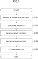
- FIGS. 1 to 5 An example of a substrate processing method according to a first embodiment will be described with reference to FIGS. 1 to 5 .
- FIG. 1 is an example of a flowchart illustrating the substrate processing method according to the first embodiment.
- step S101 a process (a MOR film formation process) of forming, on a substrate including an underlayer, a metal oxide resist film (hereinafter, also referred to as a MOR film) 640 made of a metal oxide is performed.
- a MOR film formation process a process of forming, on a substrate including an underlayer, a metal oxide resist film (hereinafter, also referred to as a MOR film) 640 made of a metal oxide is performed.
- FIG. 2 is an example of a schematic cross-sectional view of the substrate after the MOR film formation process.
- the substrate before the MOR film formation process includes a base material 610 and an underlayer (an organic film 620 and a silicon-containing film 630).
- the base material 610 is made of, for example, Si, SiO 2 , SiN, TiN, or the like.
- the underlayer is formed on the base material 610.
- a laminated structure of the organic film 620 and the silicon-containing film 630 is formed.
- the organic film 620 is formed on the base material 610.
- the organic film 620 is, for example, a carbon film.
- the silicon-containing film 630 is formed on the organic film 620.
- the silicon-containing film 630 is, for example, a spin on glass (SOG) film.
- the silicon-containing film 630 is made of, for example, SiOC, SiOCN, SiC, TiO 2 , SnO 2 , carbon, or the like.
- the configuration of the underlayer is not limited thereto.
- the underlayer may instead be only the organic film 620 or the silicon-containing film 630.
- the MOR film 640 is formed on the underlayer of the substrate. In the example illustrated in FIG. 2 , the MOR film 640 is formed on the silicon-containing film 630.
- the MOR film 640 is made of a metal oxide containing at least a metal atom and an oxygen atom (0). Alternatively, the MOR film 640 may be a metal oxide containing an alkyl group.
- the metal atom included in the MOR film 640 includes at least one of, for example, Sn, Sb, In, Ti, Zr, Hf, V, Co, Mo, W, Al, Ga, Si, Ge, P, As, Y, La, Ce, Lu, or the like.
- a method of forming the MOR film 640 may be, for example, forming by plasma chemical vapor deposition (CVD) using an organic metal-containing gas and an oxidizing gas.
- the organic metal-containing gas contains an alkyl group and a metal atom.
- the organic metal-containing gas for example, at least one of trimethyltin chloride (Me 3 SnCl), dimethyltin dichloride (Me 2 SnCl 2 ), methyltin trichloride (MeSnCl 3 ), tris (dimethylamino) methyltin (IV) ((Me 2 N) 3 SnMe), (dimethylamino) trimethyltin (IV) ((Me 2 N)SnMe 3 ), or the like can be used.
- the oxidizing gas contains an oxygen atom (0).
- the oxidizing gas for example, at least one of O 2 , O 3 , H 2 O 2 , H 2 O, or the like can be used.
- the method of forming the MOR film 640 is not limited to a dry process, may be a wet process, and is not limited.
- a process of forming a pattern in the MOR film 640 is performed.
- step S102 an exposure process is performed on the substrate including the MOR film 640.
- step S103 a development process is performed on the substrate including the MOR film 640.
- the MOR film 640 may be a positive resist film in which an exposed portion in the exposure process is removed by the development process, or may be a negative resist film in which an unexposed portion in the exposure process is removed by the development process.
- FIG. 3 is an example of a schematic cross-sectional view of the substrate after the development process.
- a pattern of an opening 661 is formed in the MOR film 640 by the exposure process and the development process.
- a modification process is performed on the substrate including the MOR film 640 in which the pattern of the opening 661 has been formed.
- the modification process modifies the MOR film 640 in which the pattern has been formed.
- the modification process is an oxidation process.
- the modification process exposes the substrate to an oxygen-containing gas atmosphere.
- the oxygen-containing gas is, for example, a peroxide (H 2 O 2 ) gas, an ozone (O 3 ) gas, or both.
- the temperature of the modification process is 100 to 350°C
- the pressure is 1.2 to 120 Torr
- the processing time is 100 to 1,200 seconds.
- This further oxidizes the MOR film 640 to form a modified MOR film 645.
- the MOR film 640 is made of a metal oxide containing an alkyl group, the alkyl group is removed by the oxidation process, and oxygen atoms (O) are bonded.
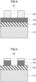
- FIG. 4 is an example of a schematic cross-sectional view of the substrate after the modification process.
- the MOR film 640 is modified by the modification process to form the modified MOR film 645.
- step S105 an etching process is performed on the substrate including the modified MOR film 645 in which the pattern of the opening 661 has been formed.
- the underlayer the silicon-containing film 630 and the organic film 620
- the modified MOR film 645 in which the pattern has been formed are etched using, as a mask, the modified MOR film 645 in which the pattern has been formed, to form a pattern in the underlayer.
- FIG. 5 is an example of a schematic cross-sectional view of the substrate after the etching process.
- a pattern of a recess 662 is formed in the silicon-containing film 630.
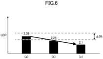
- FIG. 6 is an example of a graph indicating line edge roughness (LER) of the pattern that has been formed in the underlayer.
- step S102 and step S103 the trench-shaped pattern was formed in the MOR film 640.
- step S105 the etching process was performed on the silicon-containing film 630, which was the underlayer, using the MOR film 640 or the modified MOR film 645 having the trench-shaped pattern as a mask, thereby forming the trench-shaped pattern in the silicon-containing film 630.
- the line edge roughness (LER) in the trench-shaped pattern that had been formed in the silicon-containing film 630 was measured.
- the line edge roughness can be reduced (see the arrow in FIG. 6 ) in comparison with the case where the trench-shaped pattern is formed on the underlayer by using the MOR film 640 on which the modification process is not performed, illustrated in (a).
- the line edge roughness of the pattern formed in the underlayer can be improved.
- the organic film 620 is etched using, as a mask, the silicon-containing film 630 in which the pattern of the recess 662 has been formed, to form the pattern in the organic film 620
- the line edge roughness in the pattern formed in the organic film 620 can also be improved.
- the base material 610 is etched using, as a mask, the underlayer in which the pattern has been formed, to form a pattern in the base material 610
- the line edge roughness in the pattern formed in the base material 610 can also be improved.
- the etching resistance is also improved.
- the line width roughness (LWR) is also improved.
- FIG. 7 is an example of a flowchart illustrating the substrate processing method according to the second embodiment.
- step S201 the process (the MOR film formation process) of forming the MOR film 640 made of a metal oxide is performed on the substrate including the underlayer.
- step S202 the exposure process is performed on the substrate.
- step S203 the development process is performed on the substrate.
- the processes from step S201 to step S203 are substantially the same as the processes from step S101 to step S103 (see FIG. 1 ), and thus the duplicated description will be omitted.
- FIG. 8 is an example of a schematic cross-sectional view of the substrate before an annealing process.
- the pattern of the opening 661 is formed in the MOR film 640 by the exposure process and the development process.
- a projection 641 is formed that projects from the upper portion of the sidewall of the MOR film 640 toward the opening 661.
- the cross-sectional shape of the MOR film 640 is substantially a T-shape in which the upper portion is enlarged in the width direction.
- step S204 the annealing process is performed on the substrate.
- the annealing process is performed under the processing conditions of a substrate temperature of 150°C to 400°C, a pressure of 1 to 500 Torr, and a processing time of 30 to 60 minutes in an inert gas atmosphere.
- an inert gas N 2 gas, Ar gas, a mixture gas of N 2 gas and Ar gas, or the like can be used.
- FIG. 9 is an example of a schematic cross-sectional view of the substrate after the annealing process.
- the annealing process improves the shape of a sidewall 643 of the MOR film 640. Additionally, the residue 642 (see FIG. 8 ) on an upper surface 644 of the silicon-containing film 630 in the opening 661 is removed or reduced.
- step S205 the modification process is performed on the substrate.
- step S206 the etching process is performed on the substrate.
- the processes from step S205 to step S206 are substantially the same as the processes from step S104 to step S105 (see FIG. 1 ), and thus the duplicated description will be omitted. With this, the pattern of the recess 662 is formed in the silicon-containing film 630 (see FIG. 5 ).
- FIG. 10 is an example of a cross-sectional view of the substrate before the annealing process.
- the projection 641 is formed, projecting from the upper portion of the sidewall of the MOR film 640 toward the opening 661.
- the cross-sectional shape of the MOR film 640 is a T-shape in which the upper portion is enlarged in the width direction. Additionally, on the upper surface of the silicon-containing film 630 in the opening 661, there is the residue 642.
- FIG. 11 is an example of a cross-sectional view of the substrate after the annealing process. As illustrated in FIG. 11 , the annealing process shapes the sidewall 643 of the MOR film 640. Additionally, the residue 642 (see FIG. 8 ) is removed from the upper surface 644 of the silicon-containing film 630 in the opening 661.
- the annealing process can improve the line edge roughness (LER) of the sidewall 643 of the MOR film 640. This can also improve the line edge roughness (LER) of the recess 662 of the silicon-containing film 630 formed by the etching process using the modified MOR film 645 as a mask. Additionally, when the organic film 620 is etched using, as a mask, the silicon-containing film 630 in which the pattern of the recess 662 has been formed, to form the pattern in the organic film 620, the line edge roughness of the pattern formed in the organic film 620 can also be improved.
- LER line edge roughness
- the line edge roughness of the pattern formed in the base material 610 can also be improved.
- the line width roughness (LWR) is also improved.
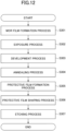
- FIG. 12 is an example of a flowchart illustrating the substrate processing method according to the third embodiment.
- step S301 the process (the MOR film formation process) of forming the MOR film 640 made of a metal oxide is performed on the substrate including the underlayer.
- step S302 the exposure process is performed on the substrate.
- step S303 the development process is performed on the substrate.
- step S304 the annealing process is performed on the substrate.
- the processes from step S301 to step S304 are substantially the same as the processes from step S201 to step S204 (see FIG. 7 ), and thus the duplicated description will be omitted.
- the annealing process in step S304 may be omitted.
- step S305 a process (a protective film formation process) of forming a protective film 650 on an upper portion of the MOR film 640 is performed.
- the protective film formation process in the step S305 also includes a modification process of the MOR film 640.
- FIG. 13 is an example of a flowchart illustrating the protective film formation process.
- step S311 the substrate is placed on a mounting section of the substrate processing apparatus.
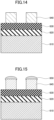
- FIG. 14 is an example of a schematic cross-sectional view of the substrate before the protective film formation process.
- the MOR film 640 in which the pattern has been formed is provided on the underlayer (the organic film 620 and the silicon-containing film 630).
- a metal-containing precursor which is a source gas, is supplied to the substrate.
- the metal-containing precursor is adsorbed on the surface of the substrate.
- the metal-containing precursor is selectively adsorbed on a non-recessed shape formed region of the MOR film 640 (the upper portion of the MOR film 640) rather than a recessed shape formed region of the MOR film 640 (a lower portion in the opening 661).
- an oxidizing gas which is a reactive gas
- a peroxide (H 2 O 2 ) gas, an ozone (O 3 ) gas, or both can be used as the oxidizing gas.
- the metal-containing precursor adsorbed on the surface of the substrate is oxidized to form the protective film 650.
- an oxidation process (corresponding to the modification process in step S104) is performed on the MOR film 640 by the oxidizing gas, and the MOR film 640 is further oxidized to form the modified MOR film 645.
- step S314 it is determined whether the processes from step S312 to step S313 have been repeated a predetermined number of times. If the processes have not been repeated the predetermined number of times (NO in S314), the processes from step S312 to step S313 are repeated. If the processes have been repeated the predetermined number of times (YES in S314), the process proceeds to step S315.
- step S315 the substrate is carried out from the substrate processing apparatus.
- FIG. 15 is an example of a schematic cross-sectional view of the substrate after the protective film formation process.
- the protective film formation process in step S305 also includes the modification process of the MOR film 640.
- the MOR film 640 (see FIG. 14 ) is modified by the oxygen-containing gas to be the modified MOR film 645.
- the protective film 650 is formed in the non-recessed shape formed region of the modified MOR film 645. In other words, the protective film 650 is formed on the upper portion of the modified MOR film 645.
- the protective film 650 is, for example, any of a titanium oxide film, a titanium oxynitride film, an aluminum oxide film, or a silicon oxide film. Additionally, the protective film 650 has a higher etching resistance than the silicon-containing film 630 under the condition of the etching process in the step S307 described later.
- step S306 the protective film shaping process is performed on the substrate.
- the protective film 650 that has been formed on the upper surface 644 of the silicon-containing film 630 is removed.
- the protective film 650 is formed thicker in the non-recessed shape formed region (the upper portion of the modified MOR film 645) than in the recessed shape formed region (the lower portion in the opening 661).
- the protective film 650 in the recessed shape formed region is removed by the etching process while the protective film 650 in the non-recessed shape formed region is left.
- step S307 the etching process is performed on the substrate.
- the process of step S307 is substantially the same as the process of step S105 (see FIG. 1 ), and thus the duplicated description will be omitted.
- the pattern of the recess 662 is formed in the silicon-containing film 630 (see FIG. 5 ).
- the protective film 650 has a higher etching resistance than the silicon-containing film 630. With this, the selectivity of the etching process is improved. Additionally, the number of steps can be reduced by collectively performing the modification process and the protective film formation process.
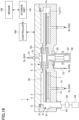
- FIG. 16 is a schematic cross-sectional view illustrating an example of the film deposition apparatus for forming the protective film 650.
- FIG. 17 is a schematic perspective view illustrating a configuration inside a vacuum chamber of the film deposition apparatus.
- FIG. 18 is a schematic plan view illustrating the configuration inside the vacuum chamber of the film deposition apparatus.
- the film deposition apparatus includes a flat vacuum chamber 1 having a substantially circular planar shape, and a rotary table 2 provided inside the vacuum chamber 1 and having a rotation center at the center of the vacuum chamber 1.
- the vacuum chamber 1 is a processing chamber for performing a film deposition process on a surface of a wafer accommodated therein.
- the vacuum chamber 1 includes a chamber body 12 having a cylindrical shape with a bottom, and a top plate 11 airtightly and detachably disposed on an upper surface of the chamber body 12 via a seal member 13 (see FIG. 16 ) such as, an O-ring.
- the rotary table 2 is fixed to a core 21 having a cylindrical shape at the center thereof, and the core 21 is fixed to an upper end of a rotary shaft 22 extending in the vertical direction.
- the rotary shaft 22 penetrates a bottom 14 of the vacuum chamber 1, and a lower end of the rotary shaft 22 is attached to a drive section 23 that rotates the rotary shaft 22 ( FIG. 16 ) around the vertical axis.
- the rotary shaft 22 and the drive section 23 are accommodated in a cylindrical case body 20 having an open upper surface.
- a flange portion provided on the upper surface of the case body 20 is airtightly attached to a lower surface of the bottom 14 of the vacuum chamber 1, and the airtight state between the internal atmosphere and the external atmosphere of the case body 20 is maintained.
- the rotary table 2 In the protective film formation process, when the protective film 650 is grown upward, the rotary table 2 is rotated at a high speed equal to or greater than 120 rpm, for example, at a predetermined speed in a range of 120 rpm to 300 rpm.
- the drive section 23 is configured to rotate the rotary table 2 at a high speed at least in a range of 120 rpm to 300 rpm.
- the protective film 650 can be selectively formed on the upper portion of the MOR film 640.
- the rotation speed of the rotary table 2 is often set to about 20 to 30 rpm. Additionally, the rotary table 2 is also configured to rotate at a low speed.
- circular recesses 24 for mounting multiple (five in the illustrated example) substrates which are semiconductor wafers (hereinafter, referred to as "wafers") W, are provided in a surface of the rotary table 2 along a rotational direction (a circumferential direction).
- wafers semiconductor wafers
- FIG. 18 the wafer W is illustrated in only one of the recesses 24 for convenience.
- the recess 24 has an inner diameter slightly greater than the diameter of the wafer W by, for example, 4mm, and a depth substantially equal to the thickness of the wafer W.
- the surface of the wafer W and the surface of the rotary table 2 are at the same height.
- Through-holes are formed in the bottom surface of the recess 24, for example.
- FIGS. 17 and 18 are views for explaining the structure in the vacuum chamber 1, and the illustration of the top plate 11 is omitted for convenience of explanation.
- a reactive gas nozzle 31, a reactive gas nozzle 32, a reactive gas nozzle 33, and separation gas nozzles 41 and 42 which are made of, for example, quartz, are arranged above the rotary table 2 at intervals in the circumferential direction of the vacuum chamber 1 (the rotational direction of the rotary table 2 (the arrow A in FIG. 18 )).
- the separation gas nozzle 41, the reactive gas nozzle 31, the separation gas nozzle 42, the reactive gas nozzle 32, and the reactive gas nozzle 33 are arranged in this order in a clockwise direction (the rotational direction of the rotary table 2).
- the nozzles 31, 32, 33, 41, and 42 are attached to be introduced from the outer circumferential wall of the vacuum chamber 1 into the vacuum chamber 1 and extend horizontally with respect to the rotary table 2 along the radial direction of the chamber body 12 by fixing gas introduction ports 31a, 32a, 33a, 41a, and 42a ( FIG. 18 ), which are base ends of the nozzles 31, 32, 33, 41, and 42, to an outer circumferential wall of the chamber body 12.
- the reactive gas nozzle 31 is connected to a supply source 130 of the source gas (the metal-containing precursor) via a pipe 110, a flow rate controller 120, and the like.
- the reactive gas nozzle 32 is connected to an oxidizing gas (H 2 O 2 , O 3 , or both) supply source 131 via a pipe 111, a flow rate controller 121, and the like.
- the reactive gas nozzle 33 is connected to an etching gas supply source 132 via a pipe 112, a flow rate controller 122, and the like.
- a halogen-based gas containing a fluorine-based gas such as CF 4 , C 2 F 6 , CH 3 F, CHF 3 , Cl 2 , ClF 3 , BCl 3 , or NF 3
- the separation gas nozzles 41 and 42 are connected to a separation gas supply source (not illustrated) via a pipe, a flow rate control valve, and the like (not illustrated).
- a rare gas such as helium (He) or argon (Ar), or an inert gas, such as nitrogen gas (N 2 ), can be used. In the present embodiment, an example of using the N 2 gas as the separation gas will be described.
- any organic metal gas or organic metalloid gas can be used from among organic metal gases or organic metalloid gases depending on the intended use.
- each of the reactive gas nozzles 31, 32, and 33 multiple gas discharge holes that are opened toward the rotary table 2 are arranged at intervals of, for example, 10 mm along the longitudinal direction of the reactive gas nozzles 31, 32, and 33.
- a region below the reactive gas nozzle 31 serves as a first processing region P1 for adsorbing the source gas onto the wafer W.
- a region below the reactive gas nozzle 32 serves as a second processing region P2 where an oxidizing gas for oxidizing the source gas adsorbed on the wafer W in the first processing region P1 is supplied to generate a molecular layer of an oxide of the organic metal or organic metalloid contained in the source gas as a reactive product.
- the molecular layer of the organic metal oxide or the organic metalloid oxide constitutes the protective film 650 to be formed.
- a region below the reactive gas nozzle 33 becomes a third processing region P3 where, after the organic metal oxide or the organic metalloid oxide (the protective film 650) generated by the oxidation has been grown upward in the second processing region P2, the unnecessary protective film 650 grown in the lateral direction is removed by etching.
- a plasma generator 80 (in FIG. 18 , the position where the plasma generator 80 is provided is illustrated by a dashed line) may be provided in the third processing region P3 as necessary.
- an activated oxygen gas may be supplied in the second processing region P2.
- an activated oxygen gas may be supplied in the second processing region P2.
- an oxygen gas activated by thermal oxidation may be supplied, or an oxygen gas activated by plasma may be supplied.
- a plasma generator may be provided in the second processing region P2.
- the first processing region P1 is a region where the source gas is adsorbed onto the wafer W, and thus may be referred to as a source gas adsorption region P1.
- the second processing region P2 is a region where the source gas adsorbed on the surface of the wafer W is oxidized, and thus may be referred to as an oxidation region P2.
- the third processing region P3 is a region where the side surface of the protective film 650 is etched, and thus may be referred to as an etching region P3.
- the plasma generator 80 it is not necessary to provide the plasma generator 80 above the third processing region P3.
- a gas having a sufficiently strong etching strength for example, ClF 3 , HF, or the like is used as an etching gas, etching can be performed without using the plasma generator 80. Therefore, the plasma generator 80 may be provided as necessary.
- the source gas supplied from the reactive gas nozzle 31 is the organic metal gas or the organic metalloid gas.
- the source gas any organic metal gas or organic metalloid gas can be used, and the source gas is selected depending on the type of the protective film to be formed.
- the organic metal gas may be a gas containing an organic metal.
- a gas containing organic amino titanium such as tetrakis(dimethylamino) titanium (TDMAT)
- TDMAT tetrakis(dimethylamino) titanium
- an organic silane gas for example, an organic aminosilane gas, such as 3DMASi, may be used.
- an organic metal or organic metalloid gas is supplied, a configuration may be used in which an organic metal or organic metalloid is vaporized by using a vaporizer or the like to generate the organic metal gas or the organic metalloid gas, and the generated organic metal gas or the organic metalloid gas is supplied into the vacuum chamber 1 by using a carrier gas, if necessary.
- any oxidizing gas may be used as long as the oxidizing gas can react with the supplied organic metal gas or organic metalloid gas to generate an organic metal oxide.
- the organic metal gas is oxidized by thermal oxidation and the MOR film 640 is also oxidized, H 2 O 2 , O 3 , or both are selected.
- any etching gas can be selected as long as the protective film formed of the organic metal oxide film or the organic metalloid oxide film can be etched.
- a fluorine-containing gas may be used.
- the fluorine-containing gas include CF 4 , ClF 3 , and the like. As described above, it may be determined whether the plasma generator 80 is provided according to the selected etching gas.
- two protrusions 4 are provided in the vacuum chamber 1.
- the protrusions 4 are attached to the back surface of the top plate 11 so as to protrude toward the rotary table 2, as described later, in order to constitute separation regions D together with the separation gas nozzles 41 and 42.
- the protrusion 4 has a fan planar shape with an apex portion being cut in an arc shape, and in the present embodiment, the protrusion 4 is disposed such that an inner arc is connected to a projection 5 (to be described later) and an outer arc is along an inner circumferential surface of the chamber body 12 of the vacuum chamber 1.
- the protrusion 4 is attached to the back surface of the top plate 11, and thus there are a flat low ceiling surface 44 (a first ceiling surface), which is a lower surface of the protrusion 4, and ceiling surfaces 45 (second ceiling surfaces), which are positioned at both sides of the ceiling surface 44 in the circumferential direction and are higher than the ceiling surface 44 in the vacuum chamber 1.
- the ceiling surface 44 has a fan planar shape with an apex portion being cut in an arc shape.
- a groove 43 is formed in the protrusion 4 at the center in the circumferential direction so as to extend in the radial direction, and the separation gas nozzle 42 is accommodated in the groove 43.
- the groove 43 is similarly formed in the other protrusion 4, and the separation gas nozzle 41 is accommodated herein.
- the reactive gas nozzles 31 and 32 are respectively provided in spaces below the high ceiling surfaces 45.
- the reactive gas nozzles 31 and 32 are provided in the vicinity of the wafer W to be spaced apart from the ceiling surfaces 45.
- the reactive gas nozzle 31 is provided in a right space below the high ceiling surface 45
- the reactive gas nozzle 32 is provided in a left space below the high ceiling surface 45.
- multiple gas discharge holes opened toward the rotary table 2 are arranged at intervals of, for example, 10 mm along the longitudinal direction of the separation gas nozzles 41 and 42.
- the ceiling surface 44 forms a separation space, which is a narrow space, with respect to the rotary table 2.
- the N 2 gas flows toward the space including the processing region P1 and the space including the processing regions P2 and P3 through the separation space.
- the volume of the separation space is smaller than the volumes of the space including the processing region P1 and the space including the processing regions P2 and P3, and thus the pressure of the separation space can be made higher than the pressures of the space including the processing region P1 and the space including the processing regions P2 and P3 by the N 2 gas. That is, a high-pressure separation space is formed between the space including the processing region P1 and the space including the processing regions P2 and P3.
- the N 2 gas flowing from the separation space to the space including the processing region P1 and the space including the processing regions P2 and P3 acts as a counter flow with respect to the source gas from the first processing region P1 and the reactive gas from the second processing region P2.
- the source gas from the first processing region P1 and the second reactive gas from the second processing region P2 are separated by the separation space. Thereby, preventing the source gas and the reactive gas from being mixed and reacting with each other in the vacuum chamber 1.
- the height of the ceiling surface 44 with respect to the upper surface of the rotary table 2 is preferably set to a height suitable for making the pressure of the separation space higher than the pressures of the space including the processing region P1 and the space including the processing regions P2 and P3 in consideration of the pressure inside the vacuum chamber 1, the rotation speed of the rotary table 2, and the supply amount of the separation gas (N 2 gas) to be supplied, during the deposition.
- the projection 5 surrounding the outer periphery of the core 21 for fixing the rotary table 2 is provided on the lower surface of the top plate 11.
- the projection 5 is continuous with a portion of the protrusion 4 on the rotation center side, and the lower surface thereof is formed at the same height as the ceiling surface 44.
- a bent portion 46 bent in an L shape is formed at a peripheral portion of the fan-shaped protrusion 4 (a portion of the vacuum chamber 1 on the outer edge side) so as to face the outer end surface of the rotary table 2.
- the bent portion 46 suppresses the reactive gas from entering from both sides of the separation region D and suppresses both of the reactive gases from being mixed, similarly to the protrusion 4.
- the fan-shaped protrusion 4 is provided on the top plate 11 and the top plate 11 is detachable from the chamber body 12, and thus a slight gap is formed between the outer peripheral surface of the bent portion 46 and the chamber body 12.
- a gap between the inner peripheral surface of the bent portion 46 and the outer end surface of the rotary table 2 and a gap between the outer peripheral surface of the bent portion 46 and the chamber body 12 are set to be the same size as the height of the ceiling surface 44 with respect to the upper surface of the rotary table 2, for example.
- An inner peripheral wall of the chamber body 12 is formed as a vertical surface close to the outer peripheral surface of the bent portion 46 in the separation region D, but is recessed outward throughout a region from a portion facing the outer end surface of the rotary table 2 to the bottom 14 in a portion other than the separation region D, as illustrated in FIG. 16 , for example.
- the recessed portion having a substantially rectangular cross-sectional shape is referred to as an exhaust region.
- the exhaust region communicating with the first processing region P1 is referred to as a first exhaust region E1
- the region communicating with the second and third processing regions P2 and P3 is referred to as a second exhaust region E2.
- a first exhaust port 61 and a second exhaust port 62 are formed in bottoms of the first exhaust region E1 and the second exhaust region E2, respectively.
- the first exhaust port 61 and the second exhaust port 62 are connected to a vacuum pump 64, which is a vacuum exhaust means, via respective exhaust pipes 63, for example.
- a pressure controller 65 is provided between the vacuum pump 64 and the exhaust pipe 63.
- a ring-shaped cover member 71 is provided below the vicinity of the periphery of the rotary table 2 to partition an atmosphere from the space above the rotary table 2 to the exhaust regions E1 and E2 from an atmosphere in which the heater unit 7 is placed, to suppress a gas from entering the region below the rotary table 2.
- the cover member 71 includes an inner member 71a provided to face an outer edge of the rotary table 2 and an outer peripheral side of the outer edge from the lower side, and an outer member (not illustrated) provided between the inner member 71a and the inner surface of the vacuum chamber 1.
- the outer member (not illustrated) is provided below the bent portion 46 and adjacent to the bent portion 46 formed at the outer edge of the protrusion 4 in the separation region D, and the inner member 71a surrounds the heater unit 7 throughout the entire circumference below the outer edge of the rotary table 2 (and below a portion slightly outside the outer edge).
- the bottom 14 at a portion closer to the rotation center than the space where the heater unit 7 is disposed projects upward to approach the core 21 near the center of the lower surface of the rotary table 2, which forms a projection 12a.
- a narrow space is formed between the projection 12a and the core 21, and a narrow gap is formed between the inner peripheral surface of the through-hole of the rotary shaft 22 passing through the bottom 14 and the rotary shaft 22, and these narrow spaces communicate with the case body 20.
- a purge gas supply pipe 72 for supplying an N 2 gas, which is a purge gas, into the narrow space to purge the narrow space is provided.
- a separation gas supply pipe 51 is connected to the center of the top plate 11 of the vacuum chamber 1, and N 2 gas, which is the separation gas, is supplied to the space between the top plate 11 and the core 21.
- the separation gas supplied to the space including a central region C is discharged toward the peripheral edge along the surface of the rotary table 2 on the wafer mounting region side via the narrow gap between the projection 5 and the rotary table 2.
- the space including the central region C may be maintained at a pressure higher than the pressure in the space including the processing region P1 and the space including the processing regions P2 and P3 by the separation gas.
- the space including the central region C suppresses the organic metal gas supplied to the first processing region P1 and the oxidizing gas supplied to the second processing region P2 from being mixed through the central region C. That is, the space including the central region C (or the central region C) can function similarly to the separation space (or the separation region D).
- a transfer port 15 for transferring the wafer W, which is the substrate, between an external transfer arm 10 and the rotary table 2 is formed in the sidewall of the vacuum chamber 1.
- the transfer port 15 is opened and closed by a gate valve (not illustrated).
- the wafer W is transferred between the recess 24, which is the wafer mounting region of the rotary table 2, and the transfer arm 10 at a position facing the transfer port 15, and thus a transfer raising/lowering pin and a raising/lowering mechanism (both not illustrated) for raising the wafer W from the back surface through the recess 24 are provided at a portion corresponding to a transfer position below the rotary table 2.
- a controller 100 formed by a computer for controlling the operation of the entire apparatus is provided, and a program for causing the film deposition apparatus to perform a protective film formation method to be described later under the control of the controller 100 is stored in a memory of the controller 100.
- the program includes steps for executing the protective film formation method to be described later, and is stored in a medium 102, such as a hard disk, a compact disc, a magneto-optical disk, a memory card, or a flexible disk, and is read into a storage unit 101 by a predetermined reading device and installed in the controller 100.
- the controller 100 may also control the rotational speed of the rotary table 2.
- the rotational speed of the rotary table 2 can be set to a high speed rotation, such as 120 rpm or greater or 120 rpm to 300 rpm as described above, or a low speed rotation, such as 60 rpm.
- controller 100 may control the flow rate controllers 120 to 122. With this, the flow rate of the gas supplied from each of the gas nozzles 31 to 33 can be controlled.
- the source gas (the metal-containing precursor) is supplied from the supply source 130 to the first processing region P1, and the oxidizing gas is supplied from the supply source 131 to the second processing region P2. Additionally, the separation gas is supplied to the separation region D.
- the wafer W which is the substrate, disposed in the recess 24 of the rotary table 2, passes through the first processing region P1 (the source gas adsorption region P1), the separation region D, the second processing region P2 (the oxidation region P2), and the separation region D every time the rotary table 2 rotates once. That is, the processes of steps S312 and S313 are repeated every time the rotary table 2 rotates. With this, the protective film 650 is formed. Additionally, by rotating the rotary table 2 at a high speed, the source gas is selectively adsorbed on the upper portion of the MOR film 640, and the protective film 650 is selectively formed on the upper portion of the MOR film 640.
- the etching gas is supplied from the supply source 132 to the third processing region P3. Additionally, the separation gas is supplied to the separation region D. With this, a portion of the protective film 650 is removed to shape the protective film 650.
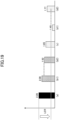
- FIG. 19 is an example of a graph indicating the line edge roughness (LER).
- the trench-shaped pattern was formed in the MOR film 640. Then, the etching process is performed on the silicon-containing film 630, which was the underlayer, using the modified MOR film 645 having the trench-shaped pattern as a mask, thereby forming the trench-shaped pattern in the silicon-containing film 630. The line edge roughness of the trench-shaped pattern formed in the silicon-containing film 630 was measured.
- FIG. 20 is a view illustrating a result of the trench shape in a case where the annealing process in step S304 is omitted and the protective film 650 is formed.
- FIG. 21 is a view illustrating a result of the trench shape in a case where the annealing process in step S304 is performed and the protective film 650 is formed.
- the protective film 650 is also formed on the projection 641 (see FIG. 8 ), and thus an overhang is formed in the protective film 650 to cover the opening 661. With this, as illustrated in FIG. 20 , a projection extending from one sidewall of the opening 661 to the other sidewall of the opening 661 appears.
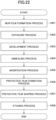
- FIG. 22 is an example of a flowchart illustrating the substrate processing method according to the fourth embodiment.
- step S401 the process (the MOR film formation process) of forming the MOR film 640 made of a metal oxide is performed on the substrate including the underlayer.
- step S402 the exposure process is performed on the substrate.
- step S403 the development process is performed on the substrate.
- step S404 the annealing process is performed on the substrate.
- step S405 the modification process is performed on the substrate.
- the processes from step S401 to step S405 are substantially the same as the processes from step S201 to step S205 (see FIG. 7 ), and thus the duplicated description will be omitted.
- the annealing process in step S404 may be omitted.
- step S406 the process (the protective film formation process) of forming the protective film 650 in the upper portion of the modified MOR film 645 is performed.
- the process in step S406 is substantially the same as the process in step S305 (see FIG. 12 ), and thus the duplicated description will be omitted.
- the description is provided assuming that the reactive gas to be reacted with the metal-containing precursor is the oxidizing gas (see step S313), but is not limited thereto.
- the reactive gas a nitriding gas may be used instead of the oxidizing gas.
- the protective film 650 is, for example, any of a titanium oxide film, a titanium oxynitride film, an aluminum oxide film, a silicon oxide film, a titanium nitride film, or a silicon nitride film. Additionally, the protective film 650 has a higher etching resistance than the silicon-containing film 630 under the condition of the etching process in step S408 described later.
- step S407 the protective film shaping process is performed on the substrate.
- step S408 the etching process is performed on the substrate.
- the processes from step S407 to step S408 are substantially the same as the processes from step S306 to step S307 (see FIG. 12 ), and thus the duplicated description will be omitted.
- the pattern of the recess 662 is formed in the silicon-containing film 630 (see FIG. 5 ).
- the protective film 650 has a higher etching resistance than the silicon-containing film 630. With this, the selectivity of the etching process is improved.
- the reactive gas for forming the protective film 650 may be the same gas as the oxidizing gas for modifying the MOR film 640, or may be a different gas.
- FIG. 23 is a block diagram illustrating the example of the substrate processing system 500.
- the substrate processing system 500 includes a substrate processing apparatus 510 and an exposure apparatus 520.
- the substrate processing apparatus 510 includes one or more processing chambers for performing one or more processes selected from a MOR film formation process 511, a development process 512, a thermal annealing process 513, a modification process 514, a protective film formation process 515, and an etching process 516.
- the exposure apparatus 520 includes a processing chamber for performing an exposure process 521.
- the substrate processing apparatus 510 and the exposure apparatus 520 may be connected in-line.
- the MOR film formation process 511, the development process 512, the thermal annealing process 513, the modification process 514, the protective film formation process 515, and the etching process 516 may be performed in different process chambers. Alternatively, multiple processes selected from the MOR film formation process 511, the development process 512, the thermal annealing process 513, the modification process 514, the protective film formation process 515, and the etching process 516 may be performed in the same process chamber.
Landscapes
- Chemical & Material Sciences (AREA)
- Organic Chemistry (AREA)
- General Physics & Mathematics (AREA)
- Physics & Mathematics (AREA)
- Metallurgy (AREA)
- Engineering & Computer Science (AREA)
- General Chemical & Material Sciences (AREA)
- Chemical Kinetics & Catalysis (AREA)
- Materials Engineering (AREA)
- Mechanical Engineering (AREA)
- Inorganic Chemistry (AREA)
- Drying Of Semiconductors (AREA)
- Manufacturing Of Printed Circuit Boards (AREA)
Abstract
Description
- The present disclosure relates to a substrate processing method and a substrate processing system.
-
Patent Document 1 andPatent Document 2 disclose substrate processing methods for patterning using a resist made of a metal oxide in EUV lithography processing. -
- Patent Document 1:
US Patent Application Publication No. 2021/305048 - Patent Document 2:
US Patent Application Publication No. 2020/326627 - In one aspect, the present disclosure provides a substrate processing method and a substrate processing system that improve line edge roughness of a pattern formed on an underlayer when the underlayer is etched using a metal oxide resist film as a mask.
- According to one aspect, in order to solve the above-described problem, a substrate processing method including a step of forming a metal oxide resist film on a substrate including an underlayer; a step of forming a pattern in the metal oxide resist film; a step of modifying the metal oxide resist film in which the pattern has been formed; and a step of etching the underlayer by using the modified metal oxide resist film as a mask is provided.
- According to one aspect, a substrate processing method and a substrate processing system that improve line edge roughness of a pattern formed on an underlayer when the underlayer is etched using a metal oxide resist film as a mask can be provided.
-
- [
FIG. 1] FIG. 1 is an example of a flowchart illustrating a substrate processing method according to a first embodiment. - [
FIG. 2] FIG. 2 is an example of a schematic cross-sectional view of a substrate after a MOR film formation process. - [
FIG. 3] FIG. 3 is an example of a schematic cross-sectional view of the substrate after a development process. - [
FIG. 4] FIG. 4 is an example of a schematic cross-sectional view of the substrate after a modification process. - [
FIG. 5] FIG. 5 is an example of a schematic cross-sectional view of the substrate after an etching process. - [
FIG. 6] FIG. 6 is an example of a graph indicating line edge roughness of a pattern formed on an underlayer. - [
FIG. 7] FIG. 7 is an example of a flowchart illustrating a substrate processing method according to a second embodiment. - [
FIG. 8] FIG. 8 is an example of a schematic cross-sectional view of the substrate before an annealing process. - [
FIG. 9] FIG. 9 is an example of a schematic cross-sectional view of the substrate after the annealing process. - [
FIG. 10] FIG. 10 is an example of a cross-sectional view of the substrate before the annealing process. - [
FIG. 11] FIG. 11 is an example of a cross-sectional view of the substrate after the annealing process. - [
FIG. 12] FIG. 12 is an example of a flowchart illustrating a substrate processing method according to a third embodiment. - [
FIG. 13] FIG. 13 is an example of a flowchart illustrating a protective film formation process. - [
FIG. 14] FIG. 14 is an example of a schematic cross-sectional view of the substrate before the protective film formation process. - [
FIG. 15] FIG. 15 is an example of a schematic cross-sectional view of the substrate after the protective film formation process. - [
FIG. 16] FIG. 16 is a schematic cross-sectional view illustrating an example of a film deposition apparatus for forming a protective film. - [
FIG. 17] FIG. 17 is a schematic perspective view illustrating a configuration inside a vacuum chamber of the film deposition apparatus. - [
FIG. 18] FIG. 18 is a schematic plan view illustrating the configuration inside the vacuum chamber of the film deposition apparatus. - [
FIG. 19] FIG. 19 is an example of a graph indicating line edge roughness. - [
FIG. 20] FIG. 20 is a view illustrating a result of a trench shape in a case where the annealing process is omitted and the protective film is formed. - [
FIG. 21] FIG. 21 is a view illustrating a result of a trench shape in a case where the annealing is performed and the protective film is formed. - [
FIG. 22] FIG. 22 is an example of a flowchart illustrating a substrate processing method according to a fourth embodiment. - [
FIG. 23] FIG. 23 is a block diagram illustrating an example of a substrate processing system. - In the following, various exemplary embodiments will be described in detail with reference to the drawings. Here, in the drawings, the same or corresponding parts are denoted by the same reference symbols.
- An example of a substrate processing method according to a first embodiment will be described with reference to
FIGS. 1 to 5 . -
FIG. 1 is an example of a flowchart illustrating the substrate processing method according to the first embodiment. - In step S101, a process (a MOR film formation process) of forming, on a substrate including an underlayer, a metal oxide resist film (hereinafter, also referred to as a MOR film) 640 made of a metal oxide is performed.
-
FIG. 2 is an example of a schematic cross-sectional view of the substrate after the MOR film formation process. - Here, the substrate before the MOR film formation process includes a
base material 610 and an underlayer (anorganic film 620 and a silicon-containing film 630). Thebase material 610 is made of, for example, Si, SiO2, SiN, TiN, or the like. The underlayer is formed on thebase material 610. In the example illustrated inFIG. 2 , as the underlayer, a laminated structure of theorganic film 620 and the silicon-containingfilm 630 is formed. Theorganic film 620 is formed on thebase material 610. Theorganic film 620 is, for example, a carbon film. The silicon-containingfilm 630 is formed on theorganic film 620. The silicon-containingfilm 630 is, for example, a spin on glass (SOG) film. The silicon-containingfilm 630 is made of, for example, SiOC, SiOCN, SiC, TiO2, SnO2, carbon, or the like. Here, the configuration of the underlayer is not limited thereto. The underlayer may instead be only theorganic film 620 or the silicon-containingfilm 630. - In the MOR film formation process, the
MOR film 640 is formed on the underlayer of the substrate. In the example illustrated inFIG. 2 , the MORfilm 640 is formed on the silicon-containingfilm 630. TheMOR film 640 is made of a metal oxide containing at least a metal atom and an oxygen atom (0). Alternatively, theMOR film 640 may be a metal oxide containing an alkyl group. The metal atom included in theMOR film 640 includes at least one of, for example, Sn, Sb, In, Ti, Zr, Hf, V, Co, Mo, W, Al, Ga, Si, Ge, P, As, Y, La, Ce, Lu, or the like. - A method of forming the
MOR film 640 may be, for example, forming by plasma chemical vapor deposition (CVD) using an organic metal-containing gas and an oxidizing gas. The organic metal-containing gas contains an alkyl group and a metal atom. As the organic metal-containing gas, for example, at least one of trimethyltin chloride (Me3SnCl), dimethyltin dichloride (Me2SnCl2), methyltin trichloride (MeSnCl3), tris (dimethylamino) methyltin (IV) ((Me2N)3SnMe), (dimethylamino) trimethyltin (IV) ((Me2N)SnMe3), or the like can be used. Additionally, the oxidizing gas contains an oxygen atom (0). As the oxidizing gas, for example, at least one of O2, O3, H2O2, H2O, or the like can be used. Additionally, the method of forming theMOR film 640 is not limited to a dry process, may be a wet process, and is not limited. - Next, a process of forming a pattern in the
MOR film 640 is performed. First, in step S102, an exposure process is performed on the substrate including theMOR film 640. Next, in step S103, a development process is performed on the substrate including theMOR film 640. Here, theMOR film 640 may be a positive resist film in which an exposed portion in the exposure process is removed by the development process, or may be a negative resist film in which an unexposed portion in the exposure process is removed by the development process. -
FIG. 3 is an example of a schematic cross-sectional view of the substrate after the development process. A pattern of anopening 661 is formed in theMOR film 640 by the exposure process and the development process. - In step S104, a modification process is performed on the substrate including the
MOR film 640 in which the pattern of theopening 661 has been formed. Here, the modification process modifies theMOR film 640 in which the pattern has been formed. Additionally, the modification process is an oxidation process. Specifically, the modification process exposes the substrate to an oxygen-containing gas atmosphere. The oxygen-containing gas is, for example, a peroxide (H2O2) gas, an ozone (O3) gas, or both. For example, the temperature of the modification process is 100 to 350°C, the pressure is 1.2 to 120 Torr, and the processing time is 100 to 1,200 seconds. This further oxidizes theMOR film 640 to form a modifiedMOR film 645. For example, when theMOR film 640 is made of a metal oxide containing an alkyl group, the alkyl group is removed by the oxidation process, and oxygen atoms (O) are bonded. -
FIG. 4 is an example of a schematic cross-sectional view of the substrate after the modification process. TheMOR film 640 is modified by the modification process to form the modifiedMOR film 645. - In step S105, an etching process is performed on the substrate including the modified
MOR film 645 in which the pattern of theopening 661 has been formed. Here, the underlayer (the silicon-containingfilm 630 and the organic film 620) are etched using, as a mask, the modifiedMOR film 645 in which the pattern has been formed, to form a pattern in the underlayer. -
FIG. 5 is an example of a schematic cross-sectional view of the substrate after the etching process. By the etching process, a pattern of arecess 662 is formed in the silicon-containingfilm 630. - Here, the linearity of an edge (sidewall) of the trench-shaped pattern formed in the underlayer will be described with reference to
FIG. 6. FIG. 6 is an example of a graph indicating line edge roughness (LER) of the pattern that has been formed in the underlayer. - Here, in step S102 and step S103, the trench-shaped pattern was formed in the
MOR film 640. Then, in step S105, the etching process was performed on the silicon-containingfilm 630, which was the underlayer, using theMOR film 640 or the modifiedMOR film 645 having the trench-shaped pattern as a mask, thereby forming the trench-shaped pattern in the silicon-containingfilm 630. The line edge roughness (LER) in the trench-shaped pattern that had been formed in the silicon-containingfilm 630 was measured. - (a) indicates the line edge roughness (LER) in a case where step S104 is omitted and the underlayer is etched using the
unmodified MOR film 640. Additionally, inFIG. 6 , a range of ±5% from the line edge roughness (LER) in (a) is illustrated by the dashed lines. - (b) indicates the line edge roughness (LER) in a case where the modification process is performed on the substrate by the hydrogen peroxide (H2O2) gas in step S104 and the underlayer is etched using the modified
MOR film 645. - (c) indicates the line edge roughness (LER) in a case where the modification process is performed on the substrate by the ozone (O3) gas in step S104 and the underlayer is etched using the modified
MOR film 645. - As illustrated in
FIG. 6 , by forming the trench-shaped pattern in the underlayer by using the modifiedMOR film 645 that is modified using the hydrogen peroxide (H2O2) gas, the ozone (O3) gas, or both illustrated in (b) and (c), the line edge roughness can be reduced (see the arrow inFIG. 6 ) in comparison with the case where the trench-shaped pattern is formed on the underlayer by using theMOR film 640 on which the modification process is not performed, illustrated in (a). - With this, the line edge roughness of the pattern formed in the underlayer can be improved. Additionally, when the
organic film 620 is etched using, as a mask, the silicon-containingfilm 630 in which the pattern of therecess 662 has been formed, to form the pattern in theorganic film 620, the line edge roughness in the pattern formed in theorganic film 620 can also be improved. Additionally, when thebase material 610 is etched using, as a mask, the underlayer in which the pattern has been formed, to form a pattern in thebase material 610, the line edge roughness in the pattern formed in thebase material 610 can also be improved. Additionally, by modifying theMOR film 640, the etching resistance is also improved. Here, as the line edge roughness is improved, the line width roughness (LWR) is also improved. - Next, an example of a substrate processing method according to a second embodiment will be described with reference to
FIGS. 7 to 9 . -
FIG. 7 is an example of a flowchart illustrating the substrate processing method according to the second embodiment. - In step S201, the process (the MOR film formation process) of forming the
MOR film 640 made of a metal oxide is performed on the substrate including the underlayer. Next, the process of forming the pattern in theMOR film 640 is performed. First, in step S202, the exposure process is performed on the substrate. Next, in step S203, the development process is performed on the substrate. Here, the processes from step S201 to step S203 are substantially the same as the processes from step S101 to step S103 (seeFIG. 1 ), and thus the duplicated description will be omitted. -
FIG. 8 is an example of a schematic cross-sectional view of the substrate before an annealing process. The pattern of theopening 661 is formed in theMOR film 640 by the exposure process and the development process. Here, aprojection 641 is formed that projects from the upper portion of the sidewall of theMOR film 640 toward theopening 661. In other words, the cross-sectional shape of theMOR film 640 is substantially a T-shape in which the upper portion is enlarged in the width direction. Additionally, on an upper surface of the silicon-containingfilm 630 in theopening 661, there is aresidue 642 due to the development process. - In step S204, the annealing process is performed on the substrate. Here, the annealing process is performed under the processing conditions of a substrate temperature of 150°C to 400°C, a pressure of 1 to 500 Torr, and a processing time of 30 to 60 minutes in an inert gas atmosphere. As the inert gas, N2 gas, Ar gas, a mixture gas of N2 gas and Ar gas, or the like can be used.
-
FIG. 9 is an example of a schematic cross-sectional view of the substrate after the annealing process. The annealing process improves the shape of asidewall 643 of theMOR film 640. Additionally, the residue 642 (seeFIG. 8 ) on anupper surface 644 of the silicon-containingfilm 630 in theopening 661 is removed or reduced. - In step S205, the modification process is performed on the substrate. Next, in step S206, the etching process is performed on the substrate. The processes from step S205 to step S206 are substantially the same as the processes from step S104 to step S105 (see
FIG. 1 ), and thus the duplicated description will be omitted. With this, the pattern of therecess 662 is formed in the silicon-containing film 630 (seeFIG. 5 ). - Here, the shapes of the formed
MOR film 640 before the annealing process and after the annealing process will be described with reference toFIGS. 10 and 11 . -
FIG. 10 is an example of a cross-sectional view of the substrate before the annealing process. As illustrated inFIG. 10 , theprojection 641 is formed, projecting from the upper portion of the sidewall of theMOR film 640 toward theopening 661. In other words, the cross-sectional shape of theMOR film 640 is a T-shape in which the upper portion is enlarged in the width direction. Additionally, on the upper surface of the silicon-containingfilm 630 in theopening 661, there is theresidue 642. -
FIG. 11 is an example of a cross-sectional view of the substrate after the annealing process. As illustrated inFIG. 11 , the annealing process shapes thesidewall 643 of theMOR film 640. Additionally, the residue 642 (seeFIG. 8 ) is removed from theupper surface 644 of the silicon-containingfilm 630 in theopening 661. - The annealing process can improve the line edge roughness (LER) of the
sidewall 643 of theMOR film 640. This can also improve the line edge roughness (LER) of therecess 662 of the silicon-containingfilm 630 formed by the etching process using the modifiedMOR film 645 as a mask. Additionally, when theorganic film 620 is etched using, as a mask, the silicon-containingfilm 630 in which the pattern of therecess 662 has been formed, to form the pattern in theorganic film 620, the line edge roughness of the pattern formed in theorganic film 620 can also be improved. Additionally, when thebase material 610 is etched using, as a mask, the underlayer in which the pattern has been formed, to form the pattern in thebase material 610, the line edge roughness of the pattern formed in thebase material 610 can also be improved. Here, as the line edge roughness is improved, the line width roughness (LWR) is also improved. - Next, an example of a substrate processing method according to a third embodiment will be described with reference to
FIGS. 12 to 15 . -
FIG. 12 is an example of a flowchart illustrating the substrate processing method according to the third embodiment. - In step S301, the process (the MOR film formation process) of forming the
MOR film 640 made of a metal oxide is performed on the substrate including the underlayer. Next, the process of forming the pattern in theMOR film 640 is performed. First, in step S302, the exposure process is performed on the substrate. Next, in step S303, the development process is performed on the substrate. Next, in step S304, the annealing process is performed on the substrate. Here, the processes from step S301 to step S304 are substantially the same as the processes from step S201 to step S204 (seeFIG. 7 ), and thus the duplicated description will be omitted. Here, the annealing process in step S304 may be omitted. - In step S305, a process (a protective film formation process) of forming a
protective film 650 on an upper portion of theMOR film 640 is performed. Here, the protective film formation process in the step S305 also includes a modification process of theMOR film 640. - Here, an example of the protective film formation process in step S305 will be described with reference to
FIG. 13. FIG. 13 is an example of a flowchart illustrating the protective film formation process. - In step S311, the substrate is placed on a mounting section of the substrate processing apparatus.
-
FIG. 14 is an example of a schematic cross-sectional view of the substrate before the protective film formation process. Here, theMOR film 640 in which the pattern has been formed is provided on the underlayer (theorganic film 620 and the silicon-containing film 630). - In step S312, a metal-containing precursor, which is a source gas, is supplied to the substrate. With this, the metal-containing precursor is adsorbed on the surface of the substrate. Here, the metal-containing precursor is selectively adsorbed on a non-recessed shape formed region of the MOR film 640 (the upper portion of the MOR film 640) rather than a recessed shape formed region of the MOR film 640 (a lower portion in the opening 661).
- In step S313, an oxidizing gas, which is a reactive gas, is supplied to the substrate. Here, as the oxidizing gas, a peroxide (H2O2) gas, an ozone (O3) gas, or both can be used. With this, the metal-containing precursor adsorbed on the surface of the substrate is oxidized to form the
protective film 650. Additionally, an oxidation process (corresponding to the modification process in step S104) is performed on theMOR film 640 by the oxidizing gas, and theMOR film 640 is further oxidized to form the modifiedMOR film 645. - In step S314, it is determined whether the processes from step S312 to step S313 have been repeated a predetermined number of times. If the processes have not been repeated the predetermined number of times (NO in S314), the processes from step S312 to step S313 are repeated. If the processes have been repeated the predetermined number of times (YES in S314), the process proceeds to step S315.
- In step S315, the substrate is carried out from the substrate processing apparatus.
-
FIG. 15 is an example of a schematic cross-sectional view of the substrate after the protective film formation process. The protective film formation process in step S305 also includes the modification process of theMOR film 640. Thus, the MOR film 640 (seeFIG. 14 ) is modified by the oxygen-containing gas to be the modifiedMOR film 645. Additionally, theprotective film 650 is formed in the non-recessed shape formed region of the modifiedMOR film 645. In other words, theprotective film 650 is formed on the upper portion of the modifiedMOR film 645. Theprotective film 650 is, for example, any of a titanium oxide film, a titanium oxynitride film, an aluminum oxide film, or a silicon oxide film. Additionally, theprotective film 650 has a higher etching resistance than the silicon-containingfilm 630 under the condition of the etching process in the step S307 described later. - In step S306, the protective film shaping process is performed on the substrate. Here, for example, the
protective film 650 that has been formed on theupper surface 644 of the silicon-containingfilm 630 is removed. For example, in step S305, theprotective film 650 is formed thicker in the non-recessed shape formed region (the upper portion of the modified MOR film 645) than in the recessed shape formed region (the lower portion in the opening 661). In step S306, theprotective film 650 in the recessed shape formed region is removed by the etching process while theprotective film 650 in the non-recessed shape formed region is left. - In step S307, the etching process is performed on the substrate. Here, the process of step S307 is substantially the same as the process of step S105 (see
FIG. 1 ), and thus the duplicated description will be omitted. With this, the pattern of therecess 662 is formed in the silicon-containing film 630 (seeFIG. 5 ). Additionally, theprotective film 650 has a higher etching resistance than the silicon-containingfilm 630. With this, the selectivity of the etching process is improved. Additionally, the number of steps can be reduced by collectively performing the modification process and the protective film formation process. - Here, an example of the substrate processing apparatus used for the protective film formation process in step S305 will be described with reference to
FIGS. 16 to 18 .FIG. 16 is a schematic cross-sectional view illustrating an example of the film deposition apparatus for forming theprotective film 650.FIG. 17 is a schematic perspective view illustrating a configuration inside a vacuum chamber of the film deposition apparatus.FIG. 18 is a schematic plan view illustrating the configuration inside the vacuum chamber of the film deposition apparatus. - Referring to
FIGS. 16 to 18 , the film deposition apparatus includes aflat vacuum chamber 1 having a substantially circular planar shape, and a rotary table 2 provided inside thevacuum chamber 1 and having a rotation center at the center of thevacuum chamber 1. Thevacuum chamber 1 is a processing chamber for performing a film deposition process on a surface of a wafer accommodated therein. Thevacuum chamber 1 includes achamber body 12 having a cylindrical shape with a bottom, and atop plate 11 airtightly and detachably disposed on an upper surface of thechamber body 12 via a seal member 13 (seeFIG. 16 ) such as, an O-ring. - The rotary table 2 is fixed to a core 21 having a cylindrical shape at the center thereof, and the
core 21 is fixed to an upper end of arotary shaft 22 extending in the vertical direction. Therotary shaft 22 penetrates a bottom 14 of thevacuum chamber 1, and a lower end of therotary shaft 22 is attached to adrive section 23 that rotates the rotary shaft 22 (FIG. 16 ) around the vertical axis. Therotary shaft 22 and thedrive section 23 are accommodated in acylindrical case body 20 having an open upper surface. A flange portion provided on the upper surface of thecase body 20 is airtightly attached to a lower surface of the bottom 14 of thevacuum chamber 1, and the airtight state between the internal atmosphere and the external atmosphere of thecase body 20 is maintained. - In the protective film formation process, when the
protective film 650 is grown upward, the rotary table 2 is rotated at a high speed equal to or greater than 120 rpm, for example, at a predetermined speed in a range of 120 rpm to 300 rpm. Thus, thedrive section 23 is configured to rotate the rotary table 2 at a high speed at least in a range of 120 rpm to 300 rpm. By rotating the rotary table 2 at a high speed, theprotective film 650 can be selectively formed on the upper portion of theMOR film 640. Here, in a general film formation process, the rotation speed of the rotary table 2 is often set to about 20 to 30 rpm. Additionally, the rotary table 2 is also configured to rotate at a low speed. - As illustrated in
FIGS. 17 and18 ,circular recesses 24 for mounting multiple (five in the illustrated example) substrates, which are semiconductor wafers (hereinafter, referred to as "wafers") W, are provided in a surface of the rotary table 2 along a rotational direction (a circumferential direction). Here, inFIG. 18 , the wafer W is illustrated in only one of therecesses 24 for convenience. Therecess 24 has an inner diameter slightly greater than the diameter of the wafer W by, for example, 4mm, and a depth substantially equal to the thickness of the wafer W. Therefore, when the wafer W is accommodated in therecess 24, the surface of the wafer W and the surface of the rotary table 2 (the region where the wafer W is not mounted) are at the same height. Through-holes (not illustrated), through which three raising/lowering pins to support the back surface of the wafer W and raise and lower the wafer W penetrate, are formed in the bottom surface of therecess 24, for example. -
FIGS. 17 and18 are views for explaining the structure in thevacuum chamber 1, and the illustration of thetop plate 11 is omitted for convenience of explanation. As illustrated inFIGS. 17 and18 , areactive gas nozzle 31, areactive gas nozzle 32, areactive gas nozzle 33, andseparation gas nozzles FIG. 18 )). In the illustrated example, theseparation gas nozzle 41, thereactive gas nozzle 31, theseparation gas nozzle 42, thereactive gas nozzle 32, and thereactive gas nozzle 33 are arranged in this order in a clockwise direction (the rotational direction of the rotary table 2). Thenozzles vacuum chamber 1 into thevacuum chamber 1 and extend horizontally with respect to the rotary table 2 along the radial direction of thechamber body 12 by fixinggas introduction ports FIG. 18 ), which are base ends of thenozzles chamber body 12. - In the present embodiment, as illustrated in
FIG. 18 , thereactive gas nozzle 31 is connected to asupply source 130 of the source gas (the metal-containing precursor) via apipe 110, aflow rate controller 120, and the like. Thereactive gas nozzle 32 is connected to an oxidizing gas (H2O2, O3, or both)supply source 131 via a pipe 111, aflow rate controller 121, and the like. Further, thereactive gas nozzle 33 is connected to an etchinggas supply source 132 via apipe 112, aflow rate controller 122, and the like. As the etching gas, a halogen-based gas containing a fluorine-based gas, such as CF4, C2F6, CH3F, CHF3, Cl2, ClF3, BCl3, or NF3, can be used; however, there is no particular limitation as long as it can be used for etching. Theseparation gas nozzles - As the source gas supplied from the
reactive gas nozzle 31, any organic metal gas or organic metalloid gas can be used from among organic metal gases or organic metalloid gases depending on the intended use. - In each of the
reactive gas nozzles reactive gas nozzles reactive gas nozzle 31 serves as a first processing region P1 for adsorbing the source gas onto the wafer W. A region below thereactive gas nozzle 32 serves as a second processing region P2 where an oxidizing gas for oxidizing the source gas adsorbed on the wafer W in the first processing region P1 is supplied to generate a molecular layer of an oxide of the organic metal or organic metalloid contained in the source gas as a reactive product. Here, the molecular layer of the organic metal oxide or the organic metalloid oxide constitutes theprotective film 650 to be formed. A region below thereactive gas nozzle 33 becomes a third processing region P3 where, after the organic metal oxide or the organic metalloid oxide (the protective film 650) generated by the oxidation has been grown upward in the second processing region P2, the unnecessaryprotective film 650 grown in the lateral direction is removed by etching. As schematically illustrated inFIG. 18 , a plasma generator 80 (inFIG. 18 , the position where theplasma generator 80 is provided is illustrated by a dashed line) may be provided in the third processing region P3 as necessary. Additionally, in the second processing region P2, an activated oxygen gas may be supplied. For example, an oxygen gas activated by thermal oxidation may be supplied, or an oxygen gas activated by plasma may be supplied. When the oxidizing gas is activated by plasma, a plasma generator may be provided in the second processing region P2. - Here, the first processing region P1 is a region where the source gas is adsorbed onto the wafer W, and thus may be referred to as a source gas adsorption region P1. The second processing region P2 is a region where the source gas adsorbed on the surface of the wafer W is oxidized, and thus may be referred to as an oxidation region P2. Additionally, the third processing region P3 is a region where the side surface of the
protective film 650 is etched, and thus may be referred to as an etching region P3. - It is not necessary to provide the
plasma generator 80 above the third processing region P3. For example, when a gas having a sufficiently strong etching strength, for example, ClF3, HF, or the like is used as an etching gas, etching can be performed without using theplasma generator 80. Therefore, theplasma generator 80 may be provided as necessary. - As described above, the source gas supplied from the
reactive gas nozzle 31 is the organic metal gas or the organic metalloid gas. As the source gas, any organic metal gas or organic metalloid gas can be used, and the source gas is selected depending on the type of the protective film to be formed. The organic metal gas may be a gas containing an organic metal. For example, when theprotective film 650 of TiO2 is formed, a gas containing organic amino titanium, such as tetrakis(dimethylamino) titanium (TDMAT), is selected. Additionally, as the organic metalloid gas, an organic silane gas, for example, an organic aminosilane gas, such as 3DMASi, may be used. When such an organic metal gas or organic metalloid gas is supplied, a configuration may be used in which an organic metal or organic metalloid is vaporized by using a vaporizer or the like to generate the organic metal gas or the organic metalloid gas, and the generated organic metal gas or the organic metalloid gas is supplied into thevacuum chamber 1 by using a carrier gas, if necessary. - Additionally, as the oxidizing gas supplied from the
reactive gas nozzle 32, any oxidizing gas may be used as long as the oxidizing gas can react with the supplied organic metal gas or organic metalloid gas to generate an organic metal oxide. For example, when the organic metal gas is oxidized by thermal oxidation and theMOR film 640 is also oxidized, H2O2, O3, or both are selected. - As the etching gas supplied from the
reactive gas nozzle 33, any etching gas can be selected as long as the protective film formed of the organic metal oxide film or the organic metalloid oxide film can be etched. For example, a fluorine-containing gas may be used. Examples of the fluorine-containing gas include CF4, ClF3, and the like. As described above, it may be determined whether theplasma generator 80 is provided according to the selected etching gas. - Referring to
FIGS. 17 and18 , twoprotrusions 4 are provided in thevacuum chamber 1. Theprotrusions 4 are attached to the back surface of thetop plate 11 so as to protrude toward the rotary table 2, as described later, in order to constitute separation regions D together with theseparation gas nozzles protrusion 4 has a fan planar shape with an apex portion being cut in an arc shape, and in the present embodiment, theprotrusion 4 is disposed such that an inner arc is connected to a projection 5 (to be described later) and an outer arc is along an inner circumferential surface of thechamber body 12 of thevacuum chamber 1. - The
protrusion 4 is attached to the back surface of thetop plate 11, and thus there are a flat low ceiling surface 44 (a first ceiling surface), which is a lower surface of theprotrusion 4, and ceiling surfaces 45 (second ceiling surfaces), which are positioned at both sides of theceiling surface 44 in the circumferential direction and are higher than theceiling surface 44 in thevacuum chamber 1. Theceiling surface 44 has a fan planar shape with an apex portion being cut in an arc shape. Additionally, as illustrated, agroove 43 is formed in theprotrusion 4 at the center in the circumferential direction so as to extend in the radial direction, and theseparation gas nozzle 42 is accommodated in thegroove 43. Thegroove 43 is similarly formed in theother protrusion 4, and theseparation gas nozzle 41 is accommodated herein. Additionally, thereactive gas nozzles reactive gas nozzles reactive gas nozzle 31 is provided in a right space below thehigh ceiling surface 45, and thereactive gas nozzle 32 is provided in a left space below thehigh ceiling surface 45. - Additionally, in the
separation gas nozzles grooves 43 of theprotrusions 4, multiple gas discharge holes opened toward the rotary table 2 are arranged at intervals of, for example, 10 mm along the longitudinal direction of theseparation gas nozzles - The
ceiling surface 44 forms a separation space, which is a narrow space, with respect to the rotary table 2. When the N2 gas is supplied from the discharge holes of theseparation gas nozzle 42, the N2 gas flows toward the space including the processing region P1 and the space including the processing regions P2 and P3 through the separation space. At this time, the volume of the separation space is smaller than the volumes of the space including the processing region P1 and the space including the processing regions P2 and P3, and thus the pressure of the separation space can be made higher than the pressures of the space including the processing region P1 and the space including the processing regions P2 and P3 by the N2 gas. That is, a high-pressure separation space is formed between the space including the processing region P1 and the space including the processing regions P2 and P3. Additionally, the N2 gas flowing from the separation space to the space including the processing region P1 and the space including the processing regions P2 and P3 acts as a counter flow with respect to the source gas from the first processing region P1 and the reactive gas from the second processing region P2. Thus, the source gas from the first processing region P1 and the second reactive gas from the second processing region P2 are separated by the separation space. Thereby, preventing the source gas and the reactive gas from being mixed and reacting with each other in thevacuum chamber 1. - Here, the height of the
ceiling surface 44 with respect to the upper surface of the rotary table 2 is preferably set to a height suitable for making the pressure of the separation space higher than the pressures of the space including the processing region P1 and the space including the processing regions P2 and P3 in consideration of the pressure inside thevacuum chamber 1, the rotation speed of the rotary table 2, and the supply amount of the separation gas (N2 gas) to be supplied, during the deposition. - With respect to the above, the
projection 5 surrounding the outer periphery of thecore 21 for fixing the rotary table 2 is provided on the lower surface of thetop plate 11. In the present embodiment, theprojection 5 is continuous with a portion of theprotrusion 4 on the rotation center side, and the lower surface thereof is formed at the same height as theceiling surface 44. - A
bent portion 46 bent in an L shape is formed at a peripheral portion of the fan-shaped protrusion 4 (a portion of thevacuum chamber 1 on the outer edge side) so as to face the outer end surface of the rotary table 2. Thebent portion 46 suppresses the reactive gas from entering from both sides of the separation region D and suppresses both of the reactive gases from being mixed, similarly to theprotrusion 4. The fan-shapedprotrusion 4 is provided on thetop plate 11 and thetop plate 11 is detachable from thechamber body 12, and thus a slight gap is formed between the outer peripheral surface of thebent portion 46 and thechamber body 12. A gap between the inner peripheral surface of thebent portion 46 and the outer end surface of the rotary table 2 and a gap between the outer peripheral surface of thebent portion 46 and thechamber body 12 are set to be the same size as the height of theceiling surface 44 with respect to the upper surface of the rotary table 2, for example. - An inner peripheral wall of the
chamber body 12 is formed as a vertical surface close to the outer peripheral surface of thebent portion 46 in the separation region D, but is recessed outward throughout a region from a portion facing the outer end surface of the rotary table 2 to the bottom 14 in a portion other than the separation region D, as illustrated inFIG. 16 , for example. Hereinafter, for convenience of description, the recessed portion having a substantially rectangular cross-sectional shape is referred to as an exhaust region. Specifically, the exhaust region communicating with the first processing region P1 is referred to as a first exhaust region E1, and the region communicating with the second and third processing regions P2 and P3 is referred to as a second exhaust region E2. As illustrated inFIGS. 16 to 18 , afirst exhaust port 61 and asecond exhaust port 62 are formed in bottoms of the first exhaust region E1 and the second exhaust region E2, respectively. As illustrated inFIG. 16 , thefirst exhaust port 61 and thesecond exhaust port 62 are connected to avacuum pump 64, which is a vacuum exhaust means, viarespective exhaust pipes 63, for example. Additionally, apressure controller 65 is provided between thevacuum pump 64 and theexhaust pipe 63. - As illustrated in
FIG. 16 , aheater unit 7, which is a heating means, is provided in a space between the rotary table 2 and the bottom 14 of thevacuum chamber 1, and the wafer W on the rotary table 2 is heated to a temperature (for example, 150°C) determined by a process recipe via the rotary table 2. A ring-shapedcover member 71 is provided below the vicinity of the periphery of the rotary table 2 to partition an atmosphere from the space above the rotary table 2 to the exhaust regions E1 and E2 from an atmosphere in which theheater unit 7 is placed, to suppress a gas from entering the region below the rotary table 2. Thecover member 71 includes aninner member 71a provided to face an outer edge of the rotary table 2 and an outer peripheral side of the outer edge from the lower side, and an outer member (not illustrated) provided between theinner member 71a and the inner surface of thevacuum chamber 1. The outer member (not illustrated) is provided below thebent portion 46 and adjacent to thebent portion 46 formed at the outer edge of theprotrusion 4 in the separation region D, and theinner member 71a surrounds theheater unit 7 throughout the entire circumference below the outer edge of the rotary table 2 (and below a portion slightly outside the outer edge). - The bottom 14 at a portion closer to the rotation center than the space where the
heater unit 7 is disposed projects upward to approach thecore 21 near the center of the lower surface of the rotary table 2, which forms aprojection 12a. A narrow space is formed between theprojection 12a and thecore 21, and a narrow gap is formed between the inner peripheral surface of the through-hole of therotary shaft 22 passing through the bottom 14 and therotary shaft 22, and these narrow spaces communicate with thecase body 20. In thecase body 20, a purgegas supply pipe 72 for supplying an N2 gas, which is a purge gas, into the narrow space to purge the narrow space is provided. Additionally, multiple purgegas supply pipes 73 for purging the space where theheater unit 7 is disposed are provided at the bottom 14 of thevacuum chamber 1 below theheater unit 7 at predetermined angular intervals in the circumferential direction. Additionally, acover member 7a is provided between theheater unit 7 and the rotary table 2 to cover a space from an inner peripheral wall (an upper surface of theinner member 71a) of the outer member (not illustrated) to an upper end of theprojection 12a in the circumferential direction in order to suppress the gas from entering the region where theheater unit 7 is provided. Thecover member 7a can be made of, for example, quartz. - Additionally, a configuration is used in which a separation
gas supply pipe 51 is connected to the center of thetop plate 11 of thevacuum chamber 1, and N2 gas, which is the separation gas, is supplied to the space between thetop plate 11 and thecore 21. The separation gas supplied to the space including a central region C is discharged toward the peripheral edge along the surface of the rotary table 2 on the wafer mounting region side via the narrow gap between theprojection 5 and the rotary table 2. The space including the central region C may be maintained at a pressure higher than the pressure in the space including the processing region P1 and the space including the processing regions P2 and P3 by the separation gas. Therefore, the space including the central region C suppresses the organic metal gas supplied to the first processing region P1 and the oxidizing gas supplied to the second processing region P2 from being mixed through the central region C. That is, the space including the central region C (or the central region C) can function similarly to the separation space (or the separation region D). - Further, as illustrated in
FIGS. 17 and18 , atransfer port 15 for transferring the wafer W, which is the substrate, between anexternal transfer arm 10 and the rotary table 2 is formed in the sidewall of thevacuum chamber 1. Thetransfer port 15 is opened and closed by a gate valve (not illustrated). Additionally, the wafer W is transferred between therecess 24, which is the wafer mounting region of the rotary table 2, and thetransfer arm 10 at a position facing thetransfer port 15, and thus a transfer raising/lowering pin and a raising/lowering mechanism (both not illustrated) for raising the wafer W from the back surface through therecess 24 are provided at a portion corresponding to a transfer position below the rotary table 2. - Additionally, as illustrated in
FIG. 16 , in the film deposition apparatus according to the present embodiment, acontroller 100 formed by a computer for controlling the operation of the entire apparatus is provided, and a program for causing the film deposition apparatus to perform a protective film formation method to be described later under the control of thecontroller 100 is stored in a memory of thecontroller 100. The program includes steps for executing the protective film formation method to be described later, and is stored in a medium 102, such as a hard disk, a compact disc, a magneto-optical disk, a memory card, or a flexible disk, and is read into astorage unit 101 by a predetermined reading device and installed in thecontroller 100. - Here, the
controller 100 may also control the rotational speed of the rotary table 2. With this, the rotational speed of the rotary table 2 can be set to a high speed rotation, such as 120 rpm or greater or 120 rpm to 300 rpm as described above, or a low speed rotation, such as 60 rpm. - Additionally, the
controller 100 may control theflow rate controllers 120 to 122. With this, the flow rate of the gas supplied from each of thegas nozzles 31 to 33 can be controlled. - With such a configuration, in the protective film formation process in step S305, the source gas (the metal-containing precursor) is supplied from the
supply source 130 to the first processing region P1, and the oxidizing gas is supplied from thesupply source 131 to the second processing region P2. Additionally, the separation gas is supplied to the separation region D. The wafer W, which is the substrate, disposed in therecess 24 of the rotary table 2, passes through the first processing region P1 (the source gas adsorption region P1), the separation region D, the second processing region P2 (the oxidation region P2), and the separation region D every time the rotary table 2 rotates once. That is, the processes of steps S312 and S313 are repeated every time the rotary table 2 rotates. With this, theprotective film 650 is formed. Additionally, by rotating the rotary table 2 at a high speed, the source gas is selectively adsorbed on the upper portion of theMOR film 640, and theprotective film 650 is selectively formed on the upper portion of theMOR film 640. - Additionally, in the protective film shaping process in step S306, the etching gas is supplied from the
supply source 132 to the third processing region P3. Additionally, the separation gas is supplied to the separation region D. With this, a portion of theprotective film 650 is removed to shape theprotective film 650. - Next, the linearity of the edge (the sidewall) of the trench-shaped pattern will be further described with reference to
FIG. 19. FIG. 19 is an example of a graph indicating the line edge roughness (LER). - Here, the trench-shaped pattern was formed in the
MOR film 640. Then, the etching process is performed on the silicon-containingfilm 630, which was the underlayer, using the modifiedMOR film 645 having the trench-shaped pattern as a mask, thereby forming the trench-shaped pattern in the silicon-containingfilm 630. The line edge roughness of the trench-shaped pattern formed in the silicon-containingfilm 630 was measured. - (a) indicates the line edge roughness (LER) in a case where the underlayer is etched using the
unmodified MOR film 640. - (b1) and (b2) indicate the line edge roughness (LER) in a case where the underlayer is etched using the modified
MOR film 645 without forming theprotective film 650. Here, the mean value of (b1) and (b2) is illustrated by the dashed line. - (c) indicates the line edge roughness (LER) in a case where the underlayer is etched using the modified
MOR film 645 in which theprotective film 650 has been formed. - (d1) and (d2) indicate the line edge roughness (LER) in a case where the protective film shaping process illustrated in step S306 is performed and the underlayer is etched using the modified
MOR film 645 in which the protective film 350 has been formed. The mean value of (d1) and (d2) is illustrated by the dashed line. - As indicated by comparing (a), (b1), and (b2), it is indicated that the line edge roughness (LER) is improved by forming the pattern of the
recess 662 in the silicon-containingfilm 630. - Further, as indicated by comparing (b1), (b2), and (c), it is indicated that the line edge roughness (LER) is further improved by forming the
protective film 650. - As indicated by comparing (c), (d1), and (d2), it is indicated that the line edge roughness (LER) is further improved by performing the protective film shaping process (see step S306). Therefore, in comparison with the case of forming the trench-shaped pattern in the underlayer by using the
MOR film 640 on which the modification process is not performed as illustrated in (a), the line edge roughness can be reduced (see the arrow ofFIG. 19 ). -
FIG. 20 is a view illustrating a result of the trench shape in a case where the annealing process in step S304 is omitted and theprotective film 650 is formed.FIG. 21 is a view illustrating a result of the trench shape in a case where the annealing process in step S304 is performed and theprotective film 650 is formed. - In the case where the annealing process is omitted and the
protective film 650 is formed, theprotective film 650 is also formed on the projection 641 (seeFIG. 8 ), and thus an overhang is formed in theprotective film 650 to cover theopening 661. With this, as illustrated inFIG. 20 , a projection extending from one sidewall of theopening 661 to the other sidewall of theopening 661 appears. - In contrast, in the case where the annealing process is performed and the
protective film 650 is formed, overhang of theprotective film 650 is suppressed. - Next, an example of a substrate processing method according to a fourth embodiment will be described with reference to
FIG. 22 . -
FIG. 22 is an example of a flowchart illustrating the substrate processing method according to the fourth embodiment. - In step S401, the process (the MOR film formation process) of forming the
MOR film 640 made of a metal oxide is performed on the substrate including the underlayer. Next, the process of forming the pattern in theMOR film 640 is performed. First, in step S402, the exposure process is performed on the substrate. Next, in step S403, the development process is performed on the substrate. Next, in step S404, the annealing process is performed on the substrate. Next, in step S405, the modification process is performed on the substrate. Here, the processes from step S401 to step S405 are substantially the same as the processes from step S201 to step S205 (seeFIG. 7 ), and thus the duplicated description will be omitted. Here, the annealing process in step S404 may be omitted. - In step S406, the process (the protective film formation process) of forming the
protective film 650 in the upper portion of the modifiedMOR film 645 is performed. Here, the process in step S406 is substantially the same as the process in step S305 (seeFIG. 12 ), and thus the duplicated description will be omitted. Additionally, in the flowchart ofFIG. 13 , the description is provided assuming that the reactive gas to be reacted with the metal-containing precursor is the oxidizing gas (see step S313), but is not limited thereto. As the reactive gas, a nitriding gas may be used instead of the oxidizing gas. Here, theprotective film 650 is, for example, any of a titanium oxide film, a titanium oxynitride film, an aluminum oxide film, a silicon oxide film, a titanium nitride film, or a silicon nitride film. Additionally, theprotective film 650 has a higher etching resistance than the silicon-containingfilm 630 under the condition of the etching process in step S408 described later. - In step S407, the protective film shaping process is performed on the substrate. In step S408, the etching process is performed on the substrate. Here, the processes from step S407 to step S408 are substantially the same as the processes from step S306 to step S307 (see
FIG. 12 ), and thus the duplicated description will be omitted. With this, the pattern of therecess 662 is formed in the silicon-containing film 630 (seeFIG. 5 ). Additionally, theprotective film 650 has a higher etching resistance than the silicon-containingfilm 630. With this, the selectivity of the etching process is improved. Additionally, according to the substrate processing method of the fourth embodiment, the reactive gas for forming theprotective film 650 may be the same gas as the oxidizing gas for modifying theMOR film 640, or may be a different gas. - Next, an example of a
substrate processing system 500 will be described with reference toFIG. 23. FIG. 23 is a block diagram illustrating the example of thesubstrate processing system 500. - The
substrate processing system 500 includes asubstrate processing apparatus 510 and anexposure apparatus 520. Thesubstrate processing apparatus 510 includes one or more processing chambers for performing one or more processes selected from a MORfilm formation process 511, adevelopment process 512, athermal annealing process 513, amodification process 514, a protectivefilm formation process 515, and anetching process 516. Theexposure apparatus 520 includes a processing chamber for performing anexposure process 521. - The
substrate processing apparatus 510 and theexposure apparatus 520 may be connected in-line. The MORfilm formation process 511, thedevelopment process 512, thethermal annealing process 513, themodification process 514, the protectivefilm formation process 515, and theetching process 516 may be performed in different process chambers. Alternatively, multiple processes selected from the MORfilm formation process 511, thedevelopment process 512, thethermal annealing process 513, themodification process 514, the protectivefilm formation process 515, and theetching process 516 may be performed in the same process chamber. - Although the embodiments and the like of the plasma processing system have been described above, the present disclosure is not limited to the above-described embodiments, and various modifications and improvements can be made within the scope of the present disclosure described in the appended claims.
- This application claims priority to
U.S. Provisional Application No. 63/366,346, filed Jun. 14, 2022 -
- 610: base material
- 620: organic film
- 630: silicon-containing film
- 640 MOR film (metal oxide resist film)
- 645 modified MOR film (metal oxide resist film)
- 641 projection
- 642 residue
- 643 sidewall
- 644 upper surface
- 650: protective film
- 661 opening
- 662 recess
Claims (10)
- A substrate processing method comprising:a step of forming a metal oxide resist film on a substrate including an underlayer;a step of forming a pattern in the metal oxide resist film;a step of modifying the metal oxide resist film in which the pattern has been formed; anda step of etching the underlayer by using the modified metal oxide resist film as a mask.
- The substrate processing method as claimed in claim 1, wherein the step of modifying the metal oxide resist film includes a process of oxidizing the metal oxide resist film.
- The substrate processing method as claimed in claim 2, wherein the step of modifying the metal oxide resist film includes a process of exposing the substrate to hydrogen peroxide, ozone, or both.
- The substrate processing method as claimed in claim 1, further comprising a step of performing an annealing process on the substrate, after the step of forming the pattern in the metal oxide resist film yet before the step of modifying the metal oxide resist film.
- The substrate processing method as claimed in claim 1, further comprising a step of forming a protective film in a non-recessed shape formed region of the metal oxide resist film after the step of forming the pattern in the metal oxide resist film,
wherein the step of forming the protective film includes:a step of providing a metal-containing precursor; anda step of supplying an oxidizing gas that also serves the step of modifying the metal oxide resist film. - The substrate processing method as claimed in claim 5, wherein the protective film is any of a titanium oxide film, a titanium oxynitride film, an aluminum oxide film, or a silicon oxide film.
- The substrate processing method as claimed in claim 1, further comprising a step of forming a protective film in a non-recessed shape formed region of the metal oxide resist film after the step of modifying the metal oxide resist film,
wherein the step of forming the protective film includes:a step of providing a metal-containing precursor; anda step of supplying a reactive gas. - The substrate processing method as claimed in claim 7, wherein the protective film is any of a titanium oxide film, a titanium oxynitride film, an aluminum oxide film, a silicon oxide film, a titanium nitride film, or a silicon nitride film.
- The substrate processing method as claimed in any one of claims 5 to 8, further comprising a step of performing a process of shaping the protective film after the step of forming the protective film yet before the step of etching the underlayer.
- A substrate processing system comprising:a film deposition apparatus configured to perform a process of forming a metal oxide resist film on a substrate including an underlayer;an exposure apparatus configured to perform an exposure process on the substrate on which the metal oxide resist film has been formed;a development apparatus configured to perform a development process on the substrate on which the exposure process has been performed;a modification apparatus configured to modify the metal oxide resist film on the substrate on which the development process has been performed; andan etching apparatus configured to etch the underlayer by using the modified metal oxide resist film as a mask.
Applications Claiming Priority (2)
| Application Number | Priority Date | Filing Date | Title |
|---|---|---|---|
| US202263366346P | 2022-06-14 | 2022-06-14 | |
| PCT/JP2023/020329 WO2023243410A1 (en) | 2022-06-14 | 2023-05-31 | Substrate processing method and substrate processing system |
Publications (2)
| Publication Number | Publication Date |
|---|---|
| EP4542627A1 true EP4542627A1 (en) | 2025-04-23 |
| EP4542627A4 EP4542627A4 (en) | 2025-11-26 |
Family
ID=89190970
Family Applications (1)
| Application Number | Title | Priority Date | Filing Date |
|---|---|---|---|
| EP23823704.4A Pending EP4542627A4 (en) | 2022-06-14 | 2023-05-31 | Substrate Processing Method and Substrate Processing System |
Country Status (7)
| Country | Link |
|---|---|
| US (1) | US20250092514A1 (en) |
| EP (1) | EP4542627A4 (en) |
| JP (1) | JPWO2023243410A1 (en) |
| KR (1) | KR20250022782A (en) |
| CN (1) | CN119343755A (en) |
| TW (1) | TW202349133A (en) |
| WO (1) | WO2023243410A1 (en) |
Families Citing this family (1)
| Publication number | Priority date | Publication date | Assignee | Title |
|---|---|---|---|---|
| WO2025177872A1 (en) * | 2024-02-21 | 2025-08-28 | 東京エレクトロン株式会社 | Plasma processing method |
Family Cites Families (8)
| Publication number | Priority date | Publication date | Assignee | Title |
|---|---|---|---|---|
| US9684234B2 (en) * | 2011-03-24 | 2017-06-20 | Uchicago Argonne, Llc | Sequential infiltration synthesis for enhancing multiple-patterning lithography |
| US10170300B1 (en) * | 2017-11-30 | 2019-01-01 | Tokyo Electron Limited | Protective film forming method |
| US10845704B2 (en) * | 2018-10-30 | 2020-11-24 | Taiwan Semiconductor Manufacturing Co., Ltd. | Extreme ultraviolet photolithography method with infiltration for enhanced sensitivity and etch resistance |
| JP7649752B2 (en) | 2019-04-12 | 2025-03-21 | インプリア・コーポレイション | Organometallic photoresist developer compositions and processing methods |
| CN114200776A (en) * | 2020-01-15 | 2022-03-18 | 朗姆研究公司 | Underlayer for photoresist adhesion and dose reduction |
| US11615958B2 (en) | 2020-03-24 | 2023-03-28 | Tokyo Electron Limited | Methods to reduce microbridge defects in EUV patterning for microelectronic workpieces |
| US12487523B2 (en) * | 2020-09-30 | 2025-12-02 | Taiwan Semiconductor Manufacturing Company, Ltd. | In-situ deposition and densification treatment for metal-comprising resist layer |
| JP7773277B2 (en) * | 2021-04-14 | 2025-11-19 | 東京エレクトロン株式会社 | Substrate processing method |
-
2023
- 2023-05-31 CN CN202380045201.0A patent/CN119343755A/en active Pending
- 2023-05-31 JP JP2024528686A patent/JPWO2023243410A1/ja active Pending
- 2023-05-31 WO PCT/JP2023/020329 patent/WO2023243410A1/en not_active Ceased
- 2023-05-31 KR KR1020257000547A patent/KR20250022782A/en active Pending
- 2023-05-31 EP EP23823704.4A patent/EP4542627A4/en active Pending
- 2023-06-06 TW TW112120941A patent/TW202349133A/en unknown
-
2024
- 2024-12-05 US US18/970,324 patent/US20250092514A1/en active Pending
Also Published As
| Publication number | Publication date |
|---|---|
| JPWO2023243410A1 (en) | 2023-12-21 |
| KR20250022782A (en) | 2025-02-17 |
| EP4542627A4 (en) | 2025-11-26 |
| WO2023243410A1 (en) | 2023-12-21 |
| US20250092514A1 (en) | 2025-03-20 |
| TW202349133A (en) | 2023-12-16 |
| CN119343755A (en) | 2025-01-21 |
Similar Documents
| Publication | Publication Date | Title |
|---|---|---|
| TWI820059B (en) | Protective film forming method | |
| JP5599350B2 (en) | Film forming apparatus and film forming method | |
| US9972500B2 (en) | Method of manufacturing semiconductor device | |
| JP6294194B2 (en) | Substrate processing method and substrate processing apparatus | |
| US20100130015A1 (en) | Patterning method | |
| KR102119299B1 (en) | Film forming apparatus | |
| JP6388553B2 (en) | Substrate processing apparatus and substrate processing method | |
| JP6388552B2 (en) | Substrate processing apparatus and substrate processing method | |
| US20240071752A1 (en) | Method of processing substrate, substrate processing apparatus, method of manufacturing semiconductor device, and recording medium | |
| KR102058264B1 (en) | Substrate processing apparatus and substrate processing method | |
| JP2017022210A (en) | Substrate processing apparatus | |
| JP2013133521A (en) | Film deposition method | |
| US9368341B2 (en) | Method of manufacturing a silicon oxide film | |
| JP6964515B2 (en) | How to clean the susceptor | |
| US20250092514A1 (en) | Substrate processing method and substrate processing system | |
| JP2017120884A (en) | Method for forming protective film | |
| JP6735549B2 (en) | Substrate processing apparatus, substrate processing method and ring-shaped member | |
| JP6071537B2 (en) | Deposition method | |
| US11710633B2 (en) | Deposition method and deposition apparatus | |
| JP5750190B2 (en) | Film forming apparatus and film forming method | |
| JP6494495B2 (en) | Substrate processing method and substrate processing apparatus | |
| JP7795162B2 (en) | Carbon film forming method and semiconductor device manufacturing method | |
| KR20230173020A (en) | Film forming method and film forming apparatus | |
| JP7744634B2 (en) | Carbon film forming method and semiconductor device manufacturing method | |
| WO2025182495A1 (en) | Film formation method and film formation device |
Legal Events
| Date | Code | Title | Description |
|---|---|---|---|
| STAA | Information on the status of an ep patent application or granted ep patent |
Free format text: STATUS: THE INTERNATIONAL PUBLICATION HAS BEEN MADE |
|
| PUAI | Public reference made under article 153(3) epc to a published international application that has entered the european phase |
Free format text: ORIGINAL CODE: 0009012 |
|
| STAA | Information on the status of an ep patent application or granted ep patent |
Free format text: STATUS: REQUEST FOR EXAMINATION WAS MADE |
|
| 17P | Request for examination filed |
Effective date: 20241230 |
|
| AK | Designated contracting states |
Kind code of ref document: A1 Designated state(s): AL AT BE BG CH CY CZ DE DK EE ES FI FR GB GR HR HU IE IS IT LI LT LU LV MC ME MK MT NL NO PL PT RO RS SE SI SK SM TR |
|
| DAV | Request for validation of the european patent (deleted) | ||
| DAX | Request for extension of the european patent (deleted) | ||
| A4 | Supplementary search report drawn up and despatched |
Effective date: 20251027 |
|
| RIC1 | Information provided on ipc code assigned before grant |
Ipc: H01L 21/3065 20060101AFI20251021BHEP Ipc: G03F 7/004 20060101ALI20251021BHEP Ipc: G03F 7/40 20060101ALI20251021BHEP Ipc: H01L 21/027 20060101ALI20251021BHEP |