EP4542622A1 - Method for producing josephson junction element and method for producing quantum bit - Google Patents
Method for producing josephson junction element and method for producing quantum bit Download PDFInfo
- Publication number
- EP4542622A1 EP4542622A1 EP22946896.2A EP22946896A EP4542622A1 EP 4542622 A1 EP4542622 A1 EP 4542622A1 EP 22946896 A EP22946896 A EP 22946896A EP 4542622 A1 EP4542622 A1 EP 4542622A1
- Authority
- EP
- European Patent Office
- Prior art keywords
- film
- substrate
- superconducting
- forming
- opening
- Prior art date
- Legal status (The legal status is an assumption and is not a legal conclusion. Google has not performed a legal analysis and makes no representation as to the accuracy of the status listed.)
- Pending
Links
Images












Classifications
-
- H—ELECTRICITY
- H10—SEMICONDUCTOR DEVICES; ELECTRIC SOLID-STATE DEVICES NOT OTHERWISE PROVIDED FOR
- H10N—ELECTRIC SOLID-STATE DEVICES NOT OTHERWISE PROVIDED FOR
- H10N60/00—Superconducting devices
- H10N60/01—Manufacture or treatment
- H10N60/0912—Manufacture or treatment of Josephson-effect devices
-
- H—ELECTRICITY
- H10—SEMICONDUCTOR DEVICES; ELECTRIC SOLID-STATE DEVICES NOT OTHERWISE PROVIDED FOR
- H10N—ELECTRIC SOLID-STATE DEVICES NOT OTHERWISE PROVIDED FOR
- H10N60/00—Superconducting devices
- H10N60/10—Junction-based devices
- H10N60/12—Josephson-effect devices
-
- H—ELECTRICITY
- H10—SEMICONDUCTOR DEVICES; ELECTRIC SOLID-STATE DEVICES NOT OTHERWISE PROVIDED FOR
- H10N—ELECTRIC SOLID-STATE DEVICES NOT OTHERWISE PROVIDED FOR
- H10N60/00—Superconducting devices
- H10N60/80—Constructional details
- H10N60/805—Constructional details for Josephson-effect devices
-
- H—ELECTRICITY
- H10—SEMICONDUCTOR DEVICES; ELECTRIC SOLID-STATE DEVICES NOT OTHERWISE PROVIDED FOR
- H10N—ELECTRIC SOLID-STATE DEVICES NOT OTHERWISE PROVIDED FOR
- H10N69/00—Integrated devices, or assemblies of multiple devices, comprising at least one superconducting element covered by group H10N60/00
Definitions
- the present invention relates to a method for manufacturing a Josephson junction device and a method for manufacturing a qubit.
- a qubit including a transmon in which a Josephson junction device and a capacitor are coupled in parallel is known.
- the Josephson junction device has a structure in which an insulating film is sandwiched between two layers of superconducting films.
- the superconducting film is formed by film formation from an oblique direction (for example, Patent Documents 1 and 2).
- a difference in a width dimension of a plurality of the superconducting films formed above a substrate may occur due to a difference in an incident angle of a film formation material to an opening of a mask layer.
- the width dimension of the plurality of superconducting films formed above the substrate is made substantially the same even in a case where the incident angle of the film formation material is different by correcting a width dimension of the opening of the mask layer (for example, Patent Document 3).
- a mask layer provided with a plurality of mask patterns each having a first opening and a second opening extending in an intersecting manner may be used.
- a first superconducting film is formed by film formation from obliquely above in a direction in which the first opening extends
- an insulating film is formed on a surface of the first superconducting film
- a second superconducting film is formed by film formation from obliquely above in a direction in which the second opening extends.
- variation in a width dimension of a plurality of the second superconducting films formed above a substrate may increase.
- an object is to suppress variation in a width dimension of a second superconducting film small.
- a method for manufacturing a Josephson junction device includes: forming, on a substrate, a mask layer in which a plurality of mask patterns, each of which has a first opening that extends in a first direction and a second opening that extends in a second direction that intersects the first direction and that intersects the first opening, is arranged in the first direction; forming, using the mask layer as a mask, a first film above the substrate by first film formation from obliquely above in the first direction, and forming, after the forming the first film, a second film above the substrate by second film formation from obliquely above in a direction different from the direction of the first film formation relative to the substrate, and forming a first superconducting film that includes the first film and the second film; forming an insulating film on a surface of the first superconducting film; and forming, using the mask layer as a mask, a third film that has a region in which the third film overlaps the first superconducting film via the insulating
- a method for manufacturing a qubit includes: forming a Josephson junction device; and forming a capacitor coupled in parallel to the Josephson junction device, and the forming the Josephson junction device includes: forming, on a substrate, a mask layer in which a plurality of mask patterns, each of which has a first opening that extends in a first direction and a second opening that extends in a second direction that intersects the first direction and that intersects the first opening, is arranged in the first direction; forming, using the mask layer as a mask, a first film above the substrate by first film formation from obliquely above in the first direction, and forming, after the forming the first film, a second film above the substrate by second film formation from obliquely above in a direction different from the direction of the first film formation relative to the substrate, and forming a first superconducting film that includes the first film and the second film; forming an insulating film on a surface of the first superconducting film; and forming, using the mask
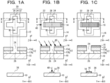
- FIGs. 1A to 2B are views illustrating the method for manufacturing the Josephson junction device according to the comparative example.
- Upper views of FIGs. 1A to 2B are plan views illustrating the method for manufacturing the Josephson junction device according to the comparative example.
- Middle views are cross-sectional views taken along a line A-A of the upper views, and lower views are cross-sectional views taken along a line B-B of the upper views.
- a first superconducting film 14, an insulating film 16, and a second superconducting film 18 formed in a gap 26 are hatched for clarity of the drawings (the same applies to the following similar drawings).
- a mask layer 12 is formed on a substrate 10.
- the mask layer 12 has an upper layer 12a and a lower layer 12b.
- a mask pattern 20 including an opening 22, an opening 24, and the gap 26 is formed in the mask layer 12.
- the opening 22 extends in an X-axis direction
- the opening 24 intersects the opening 22 and extends in a Y-axis direction, and both are formed in the upper layer 12a.
- the gap 26 is formed in the lower layer 12b.
- the gap 26 is positioned below the openings 22 and 24, and has a shape obtained by enlarging shapes of the openings 22 and 24 in plan view.
- the first superconducting film 14 is formed above the substrate 10 by film formation from obliquely above in a -X direction as indicated by an arrow 40, using the mask layer 12 as a mask.
- the first superconducting film 14 is formed by an oblique vacuum deposition method. Since the first superconducting film 14 is formed above the substrate 10 by film formation from obliquely above in the -X direction, by setting a width dimension of the opening 24 to an appropriate size, the first superconducting film 14 extending in the Y-axis direction is not formed in the gap 26. Only the first superconducting film 14 extending in the X-axis direction is formed in the gap 26.
- oxygen is introduced into a chamber to oxidize a surface of the first superconducting film 14, and the insulating film 16 is formed at the surface of the first superconducting film 14.
- the second superconducting film 18 is formed above the substrate 10 by film formation from obliquely above in a +Y direction as indicated by an arrow 42, using the mask layer 12 as a mask.
- the second superconducting film 18 is formed by the oblique vacuum deposition method. Since the second superconducting film 18 is formed above the substrate 10 by film formation from obliquely above in the +Y direction, by setting a width dimension of the opening 22 to an appropriate size, the second superconducting film 18 extending in the X-axis direction is not formed in the gap 26. Only the second superconducting film 18 extending in the Y-axis direction is formed in the gap 26. Therefore, a region 28 in which the first superconducting film 14 extending in the X-axis direction and the second superconducting film 18 extending in the Y-axis direction overlap each other via the insulating film 16 is formed.
- the mask layer 12, and the first superconducting film 14, the insulating film 16, and the second superconducting film 18 formed above the mask layer 12 are removed by a lift-off method.
- the region 28 in which the first superconducting film 14 extending in the X-axis direction and the second superconducting film 18 extending in the Y-axis direction overlap each other via the insulating film 16 becomes a Josephson junction 30.
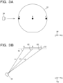
- FIGs. 3A and 3B are diagrams illustrating the oblique vacuum deposition method for film formation of the first superconducting film 14 in the method for manufacturing the Josephson junction device according to the comparative example.
- a deposition material of a deposition source 34 is vaporized or sublimated to adhere the deposition material to the substrate 10, thereby forming the first superconducting film 14.
- the deposition material of the deposition source 34 is made incident to the substrate 10 from obliquely above in the -X direction.
- a distance from the deposition source 34 to the substrate 10 greatly varies in a plane of the substrate 10.
- a distance L2 from the deposition source 34 to a central portion B of the substrate 10 a distance L1 from the deposition source 34 to an end A of the substrate 10 closer to the deposition source 34, and a distance L3 from the deposition source 34 to an end C of the substrate 10 farther from the deposition source 34 are different.
- the distance L1 is shorter than the distance L2, and the distance L2 is shorter than the distance L3.
- an angle ⁇ 2 at which the deposition material of the deposition source 34 is incident to the central portion B of the substrate 10 is 45.0°
- the distance L2 is 550 mm.
- an angle ⁇ 1 at which the deposition material is incident to the end A of the substrate 10 closer to the deposition source 34 is 47.9°
- the distance L1 is 524 mm.
- An angle ⁇ 3 at which the deposition material is incident to the end C of the substrate 10 farther from the deposition source 34 is 42.3°, and the distance L3 is 577 mm.
- FIGs. 4A to 4C are views illustrating a film thickness distribution of the first superconducting film 14 in the method for manufacturing the Josephson junction device according to the comparative example.
- Upper views of FIGs. 4A to 4C are plan views of the mask patterns 20 formed at the respective positions A to C in FIGs. 3A and 3B .
- Lower views are cross-sectional views taken along a line A-A of the upper views.
- a thickness of the first superconducting film 14 deposited at each of the positions A to C is different.
- a thickness T1 of the first superconducting film 14 deposited on the mask layer 12 at the position A is thicker than a thickness T2 of the first superconducting film 14 deposited on the mask layer 12 at the position B.
- the thickness T2 of the first superconducting film 14 deposited on the mask layer 12 at the position B is thicker than a thickness T3 of the first superconducting film 14 deposited on the mask layer 12 at the position C.
- the distances L1, L2, and L3 are 524 mm, 550 mm, and 577 mm, and the angles ⁇ 1, ⁇ 2, and ⁇ 3 are 47.9°, 45.0°, and 42.3°.
- the thickness T2 of the first superconducting film 14 at the position B is set to 28.3 nm
- the thickness T1 of the first superconducting film 14 at the position A is 31.1 nm
- the thickness T3 of the first superconducting film 14 at the position C is 25.6 nm.
- the first superconducting film 14 is deposited not only on an upper surface of the mask layer 12 but also on a side surface of the mask layer 12 in the opening 24.
- a thickness of the first superconducting film 14 on the side surface of the mask layer 12 in the opening 24 at the position A is larger than a thickness of the first superconducting film 14 on the side surface of the mask layer 12 in the opening 24 at the position B.
- the thickness of the first superconducting film 14 on the side surface of the mask layer 12 in the opening 24 at the position B is larger than a thickness of the first superconducting film 14 on the side surface of the mask layer 12 in the opening 24 at the position C.
- widths of the openings 24 formed at the respective positions A to C excluding the first superconducting films 14 are X1, X2, and X3, the width X1 is narrower than the width X2, and the width X2 is narrower than the width X3.
- FIGs. 5A to 5C are views illustrating a width distribution of the second superconducting film 18 in the method for manufacturing the Josephson junction device according to the comparative example.
- Upper views of FIGs. 5A to 5C are plan views of the mask patterns 20 formed at the respective positions A to C in FIGs. 3A and 3B .
- Lower views are cross-sectional views taken along a line A-A of the upper views.
- the width X1 of the opening 24 at the position A is narrower than the width X2 of the opening 24 at the position B
- the width X2 of the opening 24 at the position B is narrower than the width X3 of the opening 24 at the position C. Therefore, as in FIGs.
- a width W1 of the second superconducting film 18 formed in the gap 26 at the position A is narrower than a width W2 of the second superconducting film 18 formed in the gap 26 at the position B.
- the width W2 of the second superconducting film 18 formed in the gap 26 at the position B is narrower than a width W3 of the second superconducting film 18 formed in the gap 26 at the position C.
- the width dimension of the second superconducting film 18 formed in the gap 26 varies at each of the positions A to C. Therefore, an area of the region 28 where the first superconducting film 14 and the second superconducting film 18 overlap each other via the insulating film 16 (in other words, the Josephson junction 30) varies.
- a method for manufacturing a Josephson junction device according to a first embodiment capable of suppressing the variation in the width dimension of the second superconducting film 18 formed in the gap 26 and suppressing the variation in the area of the Josephson junction 30 will be indicated below.
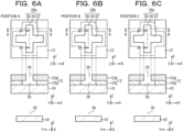
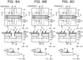
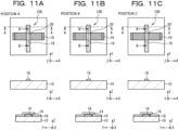
- FIGs. 6A to 11C are views illustrating the method for manufacturing the Josephson junction device according to the first embodiment.
- Upper views of FIGs. 6A , 7A , 8A , 9A , 10A , and 11A are plan views of a mask pattern 20a formed at the position A in FIGs. 3A and 3B .
- Middle views are cross-sectional views taken along a line A-A of the upper views, and lower views are cross-sectional views taken along a line B-B of the upper views.
- Upper views of FIGs. 6B , 7B , 8B , 9B , 10B , and 11B are plan views of a mask pattern 20b formed at the position B in FIGs. 3A and 3B .
- Middle views are cross-sectional views taken along the line A-A of the upper views, and lower views are cross-sectional views taken along the line B-B of the upper views.
- Upper views of FIGs. 6C , 7C , 8C , 9C , 10C , and 11C are plan views of a mask pattern 20c formed at the position C in FIGs. 3A and 3B .
- Middle views are cross-sectional views taken along the line A-A of the upper views, and lower views are cross-sectional views taken along the line B-B of the upper views.
- the mask layer 12 is formed on the substrate 10.
- the substrate 10 is, for example, a high-resistance silicon substrate.
- the mask layer 12 has an upper layer 12a and a lower layer 12b.
- the mask patterns 20a to 20c each including the opening 22, the opening 24, and the gap 26 are formed at the respective positions A to C in the mask layer 12.
- the opening 22 extends in the X-axis direction
- the opening 24 intersects (for example, is orthogonal to) the opening 22 and extends in the Y-axis direction, and both are formed in the upper layer 12a.
- the mask patterns 20a to 20c have the cross-shaped openings formed by the openings 22 and 24 in the upper layer 12a.
- the gap 26 is formed in the lower layer 12b.
- the gap 26 is positioned below the openings 22 and 24, and has the larger shape than the openings 22 and 24 in plan view.
- the mask layer 12 is formed of, for example, a resist.
- a resist having higher sensitivity to exposure for example, electron beam (EB) exposure
- EB electron beam
- the mask patterns 20a to 20c formed at the respective positions A to C are formed side by side in the X direction as in FIG. 3A .
- a first film 14a is formed above the substrate 10 by film formation from obliquely above in the -X direction as indicated by the arrow 40, using the mask layer 12 as a mask.
- the first film 14a is formed by the oblique vacuum deposition method.
- the first film 14a is, for example, an aluminum (Al) film. Since the first film 14a is formed above the substrate 10 by film formation from obliquely above in the -X direction, by setting the width dimension of the opening 24 to an appropriate size, the first film 14a extending in the Y-axis direction is not formed in the gap 26. Only the first film 14a extending in the X-axis direction is formed in the gap 26.
- the width dimension of the opening 24 smaller than a thickness dimension of the upper layer 12a, it is possible to avoid that the first film 14a extending in the Y-axis direction is formed in the gap 26.
- the first film 14a is formed to be shifted in a +X direction relative to the opening 22.
- film formation conditions are adjusted such that the thickness of the first film 14a formed at the position B is about half of the thickness of the first superconducting film 14 to be formed at the position B.
- the first film 14a is formed by film formation from obliquely above in the -X direction, a distance from the deposition source 34 is such that the first film 14a formed at the position A is closer than the first film 14a formed at the position B and the first film 14a formed at the position B is closer than the first film 14a formed at the position C. Therefore, the thickness of the first film 14a formed at the position A is larger than the thickness of the first film 14a formed at the position B. The thickness of the first film 14a formed at the position B is larger than the thickness of the first film 14a formed at the position C. In this manner, a film thickness distribution is generated in the first film 14a formed at each of the positions A to C.
- the width X1 of the opening 24 excluding the first film 14a at the position A is smaller than the width X2 of the opening 24 excluding the first film 14a at the position B.
- the width X2 of the opening 24 excluding the first film 14a at the position B is smaller than the width X3 of the opening 24 excluding the first film 14a at the position C.
- a second film 14b is formed above the substrate 10 by film formation from obliquely above in the +X direction as indicated by an arrow 41, using the mask layer 12 as a mask.
- the second film 14b is formed by the oblique vacuum deposition method.
- the second film 14b is, for example, an aluminum (Al) film. Since the second film 14b is formed above the substrate 10 by film formation from obliquely above in the +X direction, by setting the width dimension of the opening 24 to an appropriate size, the second film 14b extending in the Y-axis direction is not formed in the gap 26. Only the second film 14b extending in the X-axis direction is formed in the gap 26.
- the width dimension of the opening 24 smaller than the thickness dimension of the upper layer 12a, it is possible to avoid that the second film 14b extending in the Y-axis direction is formed in the gap 26.
- the second film 14b is formed to be shifted in the -X direction relative to the opening 22. Film formation conditions are adjusted such that a film thickness of the second film 14b formed at the position B is about half of the film thickness of the first superconducting film 14 to be formed at the position B.
- the second film 14b is formed so as to largely overlap the first film 14a, and the first superconducting film 14 is formed by the first film 14a and the second film 14b.
- the first superconducting film 14 has, for example, a width of about 100 nm to 300 nm, and the thickness of about 10 nm to 100 nm.
- FIG. 12A is a plan view after film formation of the first film 14a
- FIG. 12B is a plan view after film formation of the second film 14b.
- a lead pad 32 formed by the first film 14a and the second film 14b is also illustrated. As in FIGs.
- the first film 14a is formed to be shifted in the +X direction relative to the opening 22 (not illustrated in FIGs. 12A and 12B ), and the second film 14b is formed to be shifted in the -X direction relative to the opening 22, the first film 14a and the second film 14b are formed to be shifted in pattern in the X-axis direction.
- the second film 14b formed at the position C is closer than the second film 14b formed at the position B and the second film 14b formed at the position B is closer than the second film 14b formed at the position A. Therefore, the thickness of the second film 14b formed at the position C is larger than the thickness of the second film 14b formed at the position B. The thickness of the second film 14b formed at the position B is larger than the thickness of the second film 14b formed at the position A. In this manner, the second films 14b formed at the respective positions A to C have a film thickness distribution opposite to that of the first films 14a formed at the respective positions A to C.
- a total film thickness of the first film 14a and the second film 14b formed at each of the positions A to C has small variation.
- the variation in the thickness of the first superconducting film 14 formed at each of the positions A to C is reduced. Therefore, variation among the width X1 of the opening 24 excluding the first superconducting film 14 at the position A, the width X2 of the opening 24 excluding the first superconducting film 14 at the position B, and the width X3 of the opening 24 excluding the first superconducting film 14 at the position C is reduced.
- the thickness of the first film 14a and the thickness of the second film 14b are substantially the same in the central portion B of the substrate 10 from a viewpoint of suppressing the variation in the thickness of the first superconducting film 14 formed at each of the positions A to C using the film thickness distribution of the first film 14a and the film thickness distribution of the second film 14b.
- a ratio of a difference between the thickness of the first film 14a and the thickness of the second film 14b to the thickness of the first film 14a is set to ⁇ 3% or less.
- FIGs. 13A and 13B are diagrams illustrating the oblique vacuum deposition method for film formation of the first superconducting film 14 in the method for manufacturing the Josephson junction device according to the first embodiment.
- the first film 14a is formed above the substrate 10 by first film formation in which the deposition material of the deposition source 34 is made incident to the substrate 10 from obliquely above in the -X direction.
- the second film 14b is formed above the substrate 10 by second film formation in which the deposition material is made incident to the substrate 10 from obliquely above in the +X direction.
- an angle at which the deposition material of the deposition source 34 is incident to the end A of the substrate 10 is defined as ⁇ 11, and a distance from the deposition source 34 to the end A of the substrate 10 is defined as L11.
- An angle at which the deposition material of the deposition source 34 is incident to the central portion B of the substrate 10 is defined as ⁇ 12, and a distance from the deposition source 34 to the central portion B of the substrate 10 is defined as L12.
- An angle at which the deposition material of the deposition source 34 is incident to the end C of the substrate 10 is defined as ⁇ 13, and a distance from the deposition source 34 to the end C of the substrate 10 is defined as L13.
- an angle at which the deposition material of the deposition source 34 is incident to the end A of the substrate 10 is defined as ⁇ 21, and a distance from the deposition source 34 to the end A of the substrate 10 is defined as L21.
- An angle at which the deposition material of the deposition source 34 is incident to the central portion B of the substrate 10 is defined as ⁇ 22, and a distance from the deposition source 34 to the central portion B of the substrate 10 is defined as L22.
- An angle at which the deposition material of the deposition source 34 is incident to the end C of the substrate 10 is defined as ⁇ 23, and a distance from the deposition source 34 to the end C of the substrate 10 is defined as L23.
- the substrate 10 is a 3-inch wafer.
- the angle ⁇ 12 at which the deposition material of the deposition source 34 is incident to the central portion B of the substrate 10 is 45.0°, and the distance L12 is 550 mm.
- the angle ⁇ 11 at which the deposition material is incident to the end A of the substrate 10 is 47.9°, and the distance L11 is 524 mm.
- the angle ⁇ 13 at which the deposition material is incident to the end C of the substrate 10 is 42.3°, and the distance L13 is 577 mm.
- the angle ⁇ 22 at which the deposition material of the deposition source 34 is incident to the central portion B of the substrate 10 is 45.0°, and the distance L22 is 550 mm.
- the angle ⁇ 21 at which the deposition material is incident to the end A of the substrate 10 is 42.3°, and the distance L21 is 577 mm.
- the angle ⁇ 23 at which the deposition material is incident to the end C of the substrate 10 is 47.9°, and the distance L23 is 524 mm.
- the thickness T2 of the first film 14a deposited on the central portion B of the substrate 10 is set to 14.2 nm.
- the thickness T1 of the first film 14a deposited on the end A of the substrate 10 is about 15.6 nm
- the thickness T3 of the first film 14a deposited on the end C of the substrate 10 is about 12.8 nm (see FIGs. 7A to 7C for the thicknesses T1 to T3).
- a thickness T4 of the second film 14b deposited on the central portion B of the substrate 10 is set to 14.2 nm.
- a thickness T5 of the second film 14b deposited on the end A of the substrate 10 is about 12.8 nm
- a thickness T6 of the second film 14b deposited on the end C of the substrate 10 is about 15.6 nm (see FIGs. 8A to 8C for the thicknesses T4 to T6). Therefore, at each of the positions A to C, a thickness of a laminated film of the first film 14a and the second film 14b, in other words, the thickness of the first superconducting film 14 is about 28.3 nm, and the variation in the thickness of the first superconducting film 14 is reduced.
- the thickness of the first film 14a and the thickness of the second film 14b are somewhat affected by the incident angle at which the deposition material of the deposition source 34 is incident to the substrate 10, but are generally determined by the distance from the deposition source 34 to the substrate 10. Therefore, in order to make the thicknesses of the first film 14a and the second film 14b at the central portion B of the substrate 10 substantially the same, the distance L12 from the deposition source 34 to the central portion B in the first film formation and the distance L22 from the deposition source 34 to the central portion B in the second film formation are preferably substantially the same.
- a ratio of a difference between the distance L12 and the distance L22 to the distance L12 is set to ⁇ 5% or less.
- the incident angle of the deposition material from the deposition source 34 to the substrate 10 greatly changes, the thickness of the deposited film may change. Therefore, in order to make the thicknesses of the first film 14a and the second film 14b at the central portion B of the substrate 10 substantially the same, it is preferable that the incident angle ⁇ 12 of the deposition material to the central portion B in the first film formation and the incident angle ⁇ 22 of the deposition material to the central portion B in the second film formation are not greatly different.
- a ratio of a difference between the incident angle ⁇ 12 and the incident angle ⁇ 22 to the incident angle ⁇ 12 is set to ⁇ 30% or less.
- the second superconducting film 18 is formed above the substrate 10 by film formation from obliquely above in the +Y direction, by setting the width dimension of the opening 22 to an appropriate size, the second superconducting film 18 extending in the X-axis direction is not formed in the gap 26. Only the second superconducting film 18 extending in the Y-axis direction is formed in the gap 26. For example, by making the width dimension of the opening 22 smaller than the thickness dimension of the upper layer 12a, it is possible to avoid that the second superconducting film 18 extending in the X-axis direction is formed in the gap 26. The second superconducting film 18 is formed to be shifted in a -Y direction relative to the opening 24. Therefore, the region 28 in which the first superconducting film 14 extending in the X-axis direction and the second superconducting film 18 extending in the Y-axis direction overlap each other via the insulating film 16 is formed.
- the mask layer 12, and the first superconducting film 14, the insulating film 16, and the second superconducting film 18 formed above the mask layer 12 are removed by the lift-off method.
- the region 28 in which the first superconducting film 14 extending in the X-axis direction and the second superconducting film 18 extending in the Y-axis direction overlap each other via the insulating film 16 becomes the Josephson junction 30, and a plurality of Josephson junction devices 100 is formed on the substrate 10.
- the insulating film 16 has the thickness with which a tunnel effect may be obtained at a temperature at which superconduction occurs. Since the variation in the widths W1 to W3 of the second superconducting films 18 formed at the respective positions A to C is small, the variation in the area of the Josephson junction 30 is also small.
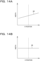
- FIG. 14A is a schematic diagram illustrating the width distribution of the second superconducting film 18 in the method for manufacturing the Josephson junction device according to the comparative example
- FIG. 14B is a schematic diagram illustrating a width distribution of the second superconducting film 18 in the method for manufacturing the Josephson junction device according to the first embodiment.
- a horizontal axis indicates a position of the substrate 10 in the X-axis direction
- a vertical axis indicates the width dimension of the second superconducting film 18.
- the width dimension of the second superconducting film 18 varies in the X-axis direction of the substrate 10.
- FIG. 14B by using the method for manufacturing the Josephson junction device according to the first embodiment, the variation in the width dimension of the second superconducting film 18 may be suppressed in the X-axis direction of the substrate 10.
- the mask layer 12 in which the plurality of mask patterns 20a to 20c each having the opening 22 extending in the X-axis direction and the opening 24 extending in the Y-axis direction and intersecting the opening 22 is arranged in the X-axis direction is formed on the substrate 10.
- the first film 14a is formed above the substrate 10 by film formation from obliquely above in the -X direction, using the mask layer 12 as a mask. Thereafter, as in FIGs.
- the second film 14b is formed above the substrate 10 by film formation from obliquely above in the +X direction 180° different from the direction of the film formation of the first film 14a relative to the substrate 10. Therefore, the first superconducting film 14 including the first film 14a and the second film 14b is formed.
- the insulating film 16 is formed on the surface of the first superconducting film 14.
- the second superconducting film 18 having the region 28 in which the second superconducting film 18 overlaps the first superconducting film 14 via the insulating film 16 above the substrate 10 by film formation from obliquely above in the +Y direction, using the mask layer 12 as a mask.
- the variation in the width dimension of the second superconducting film 18 of the plurality of Josephson junction devices 100 formed above the substrate 10 may be suppressed. Therefore, the variation in the area of the Josephson junction 30 of the plurality of Josephson junction devices 100 may be suppressed.
- the film formation of the second film 14b is performed from obliquely above in the direction 180° different from the direction of the film formation of the first film 14a relative to the substrate 10
- the present invention is not limited to this case, and the film formation of the second film 14b may be performed from obliquely above in a direction 180° ⁇ 5° different from the direction of the film formation of the first film 14a relative to the substrate 10.
- the distance L12 from the deposition source 34 to the central portion B of the substrate 10 in the film formation of the first film 14a (first film formation) is 95% or more and 105% or less of the distance L22 from the deposition source 34 to the central portion B of the substrate 10 in the film formation of the second film 14b (second film formation). Therefore, the variation in the thickness of the first superconducting film 14 in the substrate 10 may be suppressed by the film thickness distribution of the first film 14a and the film thickness distribution of the second film 14b.
- the distance L12 is preferably 97% or more and 103% or less, more preferably 98% or more and 102% or less, still more preferably 99% or more and 101% or less of the distance L22.
- the variation in the width dimension of the second superconducting film 18 of the plurality of Josephson junction devices 100 may be suppressed.
- the angle ⁇ 12 is preferably 75% or more and 125% or less, more preferably 80% or more and 120% or less, still more preferably 90% or more and 110% or less of the angle ⁇ 22.
- the thickness of the first film 14a at the central portion B of the substrate 10 is 97% or more and 103% or less of the thickness of the second film 14b at the central portion B of the substrate 10. Therefore, the variation in the thickness of the first superconducting film 14 in the substrate 10 may be suppressed by the film thickness distribution of the first film 14a and the film thickness distribution of the second film 14b. Therefore, the variation in the width dimension of the second superconducting film 18 of the plurality of Josephson junction devices 100 may be suppressed.
- the thickness of the first film 14a at the central portion B of the substrate 10 is preferably 98% or more and 102% or less, and more preferably 99% or more and 101% or less of the thickness of the second film 14b at the central portion B of the substrate 10.
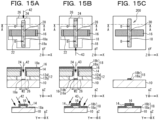
- FIGs. 15A to 15C are cross-sectional views illustrating a method for manufacturing a Josephson junction device according to a second embodiment.
- Upper views of FIGs. 15A to 15C are plan views illustrating the method for manufacturing the Josephson junction device according to the second embodiment, middle views are cross-sectional views taken along a line A-A of the upper views, and lower views are cross-sectional views taken along a line B-B of the upper views.
- steps illustrated in FIGs. 6A to 9C of the first embodiment are performed. Thereafter, as in FIG.
- a first film 18a is formed above a substrate 10 by film formation from obliquely above in the +Y direction as indicated by an arrow 42, using a mask layer 12 as a mask.
- the first film 18a is formed by the oblique vacuum deposition method.
- the first film 18a is, for example, an aluminum (Al) film.
- film formation conditions are adjusted such that a thickness of the first film 18a formed at a center of the substrate 10 is about half of a thickness of a second superconducting film 18 to be formed at the center of the substrate 10.
- a second film 18b is formed above the substrate 10 by film formation from obliquely above in the -Y direction as indicated by an arrow 43, using the mask layer 12 as a mask.
- the second film 18b is formed by the oblique vacuum deposition method.
- the second film 18b is, for example, an aluminum (Al) film.
- film formation conditions are adjusted such that a thickness of the second film 18b formed at the center of the substrate 10 is about half of the thickness of the second superconducting film 18 to be formed at the center of the substrate 10.
- the second film 18b is formed above the substrate 10 by film formation from obliquely above in the -Y direction, the second film 18b is formed to cover the side surface on the side of the -Y direction of the first superconducting film 14. Note that the second film 18b may not be formed on a side surface on a side of the +Y direction of the first superconducting film 14. The second film 18b is formed so as to largely overlap the first film 18a, and the second superconducting film 18 is formed by the first film 18a and the second film 18b.
- the second film 18b is formed above the substrate 10 by film formation from obliquely above in the -Y direction 180° different from the direction of the film formation of the first film 18a relative to the substrate 10. Therefore, the second superconducting film 18 including the first film 18a and the second film 18b is formed. In this manner, by forming the second superconducting film 18 by film formation from obliquely above in the +Y direction and the -Y direction, it is possible to suppress disconnection from occurring in the second superconducting film 18 even in a case where the first superconducting film 14 is thick.
- the film formation of the second film 18b is performed from obliquely above in the direction 180° different from the direction of the film formation of the first film 18a relative to the substrate 10 has been described as an example.
- the present invention is not limited to this case, and the film formation of the second film 18b may be performed from obliquely above in a direction 180° ⁇ 5° different from the direction of the film formation of the first film 18a relative to the substrate 10.
- FIGs. 16A and 16B are diagrams illustrating an incident angle of a deposition material to a substrate 10 in the oblique vacuum deposition method for film formation of a first superconducting film 14 and a second superconducting film 18.
- the substrate 10 is inclined relative to a deposition source 34, and a deposition material of the deposition source 34 is made incident to the substrate 10 from obliquely above in the -X direction and the +X direction to form the first superconducting film 14.
- the deposition source 34 is not positioned at infinity relative to the substrate 10, but is placed at a distance of, for example, about 500 mm from the substrate 10.
- an incident angle of the deposition material of the deposition source 34 is different in the Y-axis direction of the substrate 10.
- the incident angle of the deposition material of the deposition source 34 is different in regions A, B, and C positioned on the side of the +Y direction, regions D, E, and F positioned at a center in the Y-axis direction, and regions G, H, and I positioned on the side of the -Y direction in the substrate 10.
- the deposition material of the deposition source 34 is made incident to the substrate 10 from obliquely above in the +Y direction to form the second superconducting film 18. Therefore, as indicated by arrows 42a to 42c, the incident angle of the deposition material of the deposition source 34 is different in the X-axis direction of the substrate 10. In other words, the incident angle of the deposition material of the deposition source 34 is different in the regions A, D, and G positioned on a side of the -X direction, the regions B, E, and H positioned at the center in the X-axis direction, and the regions C, F, and I positioned on a side of the +X direction in the substrate 10.
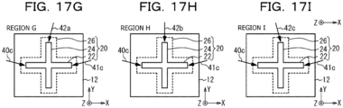
- FIGs. 17A to 17I incident angles of the deposition material to mask patterns 20 formed in the regions A to I in FIGs. 16A and 16B are illustrated.
- an opening 22 included in the mask pattern 20 extends in the X-axis direction and an opening 24 extends in the Y-axis direction in all of the regions A to I. Therefore, as in FIGs. 17D to 17F , with respect to the regions D, E, and F positioned at the center in the Y-axis direction in the substrate 10, the deposition material is incident to the opening 22 from directions substantially parallel to the X-axis direction as indicated by the arrows 40b and 41b.
- the deposition material is incident to the opening 24 from a direction substantially parallel to the Y-axis direction as indicated by the arrow 42b.
- the deposition material is incident to the opening 24 from a direction inclined in the +X direction relative to the opening 24 as indicated by the arrow 42a.
- the deposition material is incident to the opening 24 from a direction inclined in the -X direction relative to the opening 24 as indicated by the arrow 42c.
- FIGs. 18A to 18I Josephson junction devices formed in the regions A to I in FIGs. 16A and 16B are illustrated.
- the first superconducting film 14 is illustrated through the insulating film 16.
- the deposition material is incident to the opening 22 extending in the X-axis direction from the directions substantially parallel to the X-axis direction.
- the deposition material is incident to the opening 22 extending in the X-axis direction from the directions inclined in the -Y direction.
- FIGs. 17D to 17F in the regions D, E, and F
- the deposition material is incident to the opening 22 extending in the X-axis direction from the directions substantially parallel to the X-axis direction.
- the deposition material is incident to the opening 22 extending in the X-axis direction from the directions inclined in the -Y direction.
- the deposition material is incident to the opening 22 extending in the X-axis direction from the directions inclined in the +Y direction. Therefore, as in FIGs. 18A to 18I , the first superconducting films 14 formed in the regions A, B, C, G, H, and I are formed to have widths narrower than widths of the first superconducting films 14 formed in the regions D, E, and F.
- the deposition material is incident to the opening 24 extending in the Y-axis direction from the direction substantially parallel to the Y-axis direction.
- the deposition material is incident to the opening 24 extending in the Y-axis direction from the direction inclined in the +X direction.
- the deposition material is incident to the opening 24 extending in the Y-axis direction from the direction inclined in the -X direction.
- the second superconducting films 18 formed in the regions A, C, D, F, G, and I are formed to have widths narrower than widths of the second superconducting films 18 formed in the regions B, E, and H.
- FIGs. 19A to 19I are plan views illustrating the mask patterns 20 formed in the mask layer 12 in a method for manufacturing a Josephson junction device according to the third embodiment.
- the mask patterns 20 formed in the regions A to I in FIGs. 16A and 16B are illustrated.
- the openings 22 formed in the regions D, E, and F positioned at the center of substrate 10 in the Y-axis direction have widths narrower than widths of the openings 22 formed in the regions A, B, C, G, H, and I positioned at ends of the substrate 10 in the Y-axis direction.
- the widths of the openings 22 positioned at the center of the substrate 10 are narrowed, and the widths of the openings 22 positioned at the ends of the substrate 10 are widened. Therefore, even in a case where the incident angles when the deposition material of the deposition source 34 is incident to the substrate 10 from obliquely above in the -X direction and the +X direction are different in the Y-axis direction, it is possible to suppress the variation in the width dimension of the first superconducting film 14 formed above the substrate 10.
- the openings 24 formed in the regions B, E, and H positioned at the center of the substrate 10 in the X-axis direction have widths narrower than widths of the openings 24 formed in the regions A, C, D, F, G, and I positioned at the ends of the substrate 10 in the X-axis direction. In this manner, in the X-axis direction, the widths of the openings 24 positioned at the center of the substrate 10 are narrowed, and the widths of the openings 24 positioned at the ends of substrate 10 are widened.
- the opening 22 and the opening 24 extend in directions different by 90° has been described as an example.
- the opening 22 and the opening 24 may extend in a direction slightly shifted from 90° (for example, 80° to 100°).
- the case where the first superconducting film 14 and the second superconducting film 18 are formed using the oblique deposition method has been described as an example.
- the first superconducting film 14 and the second superconducting film 18 may be formed by a method other than the oblique deposition.
- the case where the first superconducting film 14 and the second superconducting film 18 are aluminum (Al) films has been described as an example.
- the first superconducting film 14 and the second superconducting film 18 may be a niobium (Nb) film, a niobium nitride (NbN) film, a tantalum (Ta) film, a tantalum nitride (TaN) film, or a titanium nitride (TiN) film.
- the case where the insulating film 16 is an oxide film of the first superconducting film 14 has been described as an example. However, other cases may be employed.
- FIG. 20A is a circuit diagram of a qubit 300 according to a fourth embodiment
- FIG. 20B is a plan view of the qubit 300 according to the fourth embodiment.
- the qubit 300 according to the fourth embodiment includes a transmon 80 including a Josephson junction device 100 formed by the manufacturing method of the first embodiment and a capacitor 82 coupled in parallel to the Josephson junction device 100.
- the Josephson junction device 100 is formed by the manufacturing method of the first embodiment, and the capacitor 82 coupled in parallel to the Josephson junction device 100 is formed.
- the capacitor 82 is formed between electrode films 84 and 86 coupled to the Josephson junction device 100 by making the electrode films 84 and 86 face each other, for example.
- Josephson junction device 100 formed by the manufacturing method of the first embodiment
- a Josephson junction device formed by the manufacturing method of the second embodiment or the third embodiment may be used.
Landscapes
- Engineering & Computer Science (AREA)
- Manufacturing & Machinery (AREA)
- Superconductor Devices And Manufacturing Methods Thereof (AREA)
Abstract
Description
- The present invention relates to a method for manufacturing a Josephson junction device and a method for manufacturing a qubit.
- A qubit including a transmon in which a Josephson junction device and a capacitor are coupled in parallel is known. The Josephson junction device has a structure in which an insulating film is sandwiched between two layers of superconducting films. It is known that the superconducting film is formed by film formation from an oblique direction (for example, Patent Documents 1 and 2). In a case where the superconducting film is formed by the film formation from the oblique direction, a difference in a width dimension of a plurality of the superconducting films formed above a substrate may occur due to a difference in an incident angle of a film formation material to an opening of a mask layer. Thus, it is known that the width dimension of the plurality of superconducting films formed above the substrate is made substantially the same even in a case where the incident angle of the film formation material is different by correcting a width dimension of the opening of the mask layer (for example, Patent Document 3).
- When the Josephson junction device is manufactured, a mask layer provided with a plurality of mask patterns each having a first opening and a second opening extending in an intersecting manner may be used. In this case, a first superconducting film is formed by film formation from obliquely above in a direction in which the first opening extends, an insulating film is formed on a surface of the first superconducting film, and then a second superconducting film is formed by film formation from obliquely above in a direction in which the second opening extends. However, in such a method, variation in a width dimension of a plurality of the second superconducting films formed above a substrate may increase.
- In one aspect, an object is to suppress variation in a width dimension of a second superconducting film small.
- In one aspect, a method for manufacturing a Josephson junction device includes: forming, on a substrate, a mask layer in which a plurality of mask patterns, each of which has a first opening that extends in a first direction and a second opening that extends in a second direction that intersects the first direction and that intersects the first opening, is arranged in the first direction; forming, using the mask layer as a mask, a first film above the substrate by first film formation from obliquely above in the first direction, and forming, after the forming the first film, a second film above the substrate by second film formation from obliquely above in a direction different from the direction of the first film formation relative to the substrate, and forming a first superconducting film that includes the first film and the second film; forming an insulating film on a surface of the first superconducting film; and forming, using the mask layer as a mask, a third film that has a region in which the third film overlaps the first superconducting film via the insulating film above the substrate by third film formation from obliquely above in the second direction, and forming a second superconducting film that includes the third film.
- In one aspect, a method for manufacturing a qubit includes: forming a Josephson junction device; and forming a capacitor coupled in parallel to the Josephson junction device, and the forming the Josephson junction device includes: forming, on a substrate, a mask layer in which a plurality of mask patterns, each of which has a first opening that extends in a first direction and a second opening that extends in a second direction that intersects the first direction and that intersects the first opening, is arranged in the first direction; forming, using the mask layer as a mask, a first film above the substrate by first film formation from obliquely above in the first direction, and forming, after the forming the first film, a second film above the substrate by second film formation from obliquely above in a direction different from the direction of the first film formation relative to the substrate, and forming a first superconducting film that includes the first film and the second film; forming an insulating film on a surface of the first superconducting film; and forming, using the mask layer as a mask, a third film that has a region in which the third film overlaps the first superconducting film via the insulating film above the substrate by third film formation from obliquely above in the second direction, and forming a second superconducting film that includes the third film.
- As one aspect, it is possible to suppress variation in a width dimension of a second superconducting film small.
-
-
FIGs. 1A to 1C are views (part 1) illustrating a method for manufacturing a Josephson junction device according to a comparative example. -
FIGs. 2A and 2B are views (part 2) illustrating the method for manufacturing the Josephson junction device according to the comparative example. -
FIGs. 3A and 3B are diagrams illustrating an oblique vacuum deposition method for film formation of a first superconducting film in the manufacturing method of the comparative example. -
FIGs. 4A to 4C are views illustrating a film thickness distribution of the first superconducting film in the manufacturing method of the comparative example. -
FIGs. 5A to 5C are views illustrating a width distribution of a second superconducting film in the manufacturing method of the comparative example. -
FIGs. 6A to 6C are views (part 1) illustrating a method for manufacturing a Josephson junction device according to a first embodiment. -
FIGs. 7A to 7C are views (part 2) illustrating the method for manufacturing the Josephson junction device according to the first embodiment. -
FIGs. 8A to 8C are views (part 3) illustrating the method for manufacturing the Josephson junction device according to the first embodiment. -
FIGs. 9A to 9C are views (part 4) illustrating the method for manufacturing the Josephson junction device according to the first embodiment. -
FIGs. 10A to 10C are views (part 5) illustrating the method for manufacturing the Josephson junction device according to the first embodiment. -
FIGs. 11A to 11C are views (part 6) illustrating the method for manufacturing the Josephson junction device according to the first embodiment. -
FIG. 12A is a plan view after film formation of a first film of a first superconducting film, andFIG. 12B is a plan view after film formation of a second film of the first superconducting film. -
FIGs. 13A and 13B are diagrams illustrating an oblique vacuum deposition method for film formation of the first superconducting film in the manufacturing method of the first embodiment. -
FIG. 14A is a schematic diagram illustrating the width distribution of the second superconducting film in the manufacturing method of the comparative example, andFIG. 14B is a schematic diagram illustrating a width distribution of a second superconducting film in the manufacturing method of the first embodiment. -
FIGs. 15A to 15C are cross-sectional views illustrating a method for manufacturing a Josephson junction device according to a second embodiment. -
FIGs. 16A and 16B are diagrams illustrating an incident angle of a deposition material to a substrate in an oblique vacuum deposition method for film formation of a first superconducting film and a second superconducting film. -
FIGs. 17A to 17I are views illustrating incident angles of the deposition material to mask patterns formed in regions A to I inFIGs. 16A and 16B . -
FIGs. 18A to 18I are views illustrating the Josephson junction devices formed in the regions A to I inFIGs. 16A and 16B . -
FIGs. 19A to 19I are plan views illustrating mask patterns formed on a mask layer in a method for manufacturing a Josephson junction device according to a third embodiment. -
FIG. 20A is a circuit diagram of a qubit according to a fourth embodiment, andFIG. 20B is a plan view of the qubit according to the fourth embodiment. - Hereinafter, embodiments of the present invention will be described with reference to the drawings.
- A method for manufacturing a Josephson junction device referred to as a Manhattan type will be described. First, a method for manufacturing a Josephson junction device according to a comparative example will be described.
FIGs. 1A to 2B are views illustrating the method for manufacturing the Josephson junction device according to the comparative example. Upper views ofFIGs. 1A to 2B are plan views illustrating the method for manufacturing the Josephson junction device according to the comparative example. Middle views are cross-sectional views taken along a line A-A of the upper views, and lower views are cross-sectional views taken along a line B-B of the upper views. In the upper plan views ofFIGs. 1B to 2B , afirst superconducting film 14, an insulatingfilm 16, and asecond superconducting film 18 formed in agap 26 are hatched for clarity of the drawings (the same applies to the following similar drawings). - As in
FIG. 1A , amask layer 12 is formed on asubstrate 10. Themask layer 12 has anupper layer 12a and alower layer 12b. Amask pattern 20 including anopening 22, anopening 24, and thegap 26 is formed in themask layer 12. Theopening 22 extends in an X-axis direction, theopening 24 intersects theopening 22 and extends in a Y-axis direction, and both are formed in theupper layer 12a. Thegap 26 is formed in thelower layer 12b. Thegap 26 is positioned below theopenings openings - As in
FIG. 1B , thefirst superconducting film 14 is formed above thesubstrate 10 by film formation from obliquely above in a -X direction as indicated by anarrow 40, using themask layer 12 as a mask. For example, thefirst superconducting film 14 is formed by an oblique vacuum deposition method. Since thefirst superconducting film 14 is formed above thesubstrate 10 by film formation from obliquely above in the -X direction, by setting a width dimension of theopening 24 to an appropriate size, thefirst superconducting film 14 extending in the Y-axis direction is not formed in thegap 26. Only thefirst superconducting film 14 extending in the X-axis direction is formed in thegap 26. - As in
FIG. 1C , while maintaining a vacuum state when thefirst superconducting film 14 is formed, oxygen is introduced into a chamber to oxidize a surface of thefirst superconducting film 14, and the insulatingfilm 16 is formed at the surface of thefirst superconducting film 14. - As in
FIG. 2A , thesecond superconducting film 18 is formed above thesubstrate 10 by film formation from obliquely above in a +Y direction as indicated by anarrow 42, using themask layer 12 as a mask. For example, thesecond superconducting film 18 is formed by the oblique vacuum deposition method. Since thesecond superconducting film 18 is formed above thesubstrate 10 by film formation from obliquely above in the +Y direction, by setting a width dimension of theopening 22 to an appropriate size, thesecond superconducting film 18 extending in the X-axis direction is not formed in thegap 26. Only thesecond superconducting film 18 extending in the Y-axis direction is formed in thegap 26. Therefore, aregion 28 in which thefirst superconducting film 14 extending in the X-axis direction and thesecond superconducting film 18 extending in the Y-axis direction overlap each other via the insulatingfilm 16 is formed. - As in
FIG. 2B , themask layer 12, and thefirst superconducting film 14, the insulatingfilm 16, and thesecond superconducting film 18 formed above themask layer 12 are removed by a lift-off method. Theregion 28 in which thefirst superconducting film 14 extending in the X-axis direction and thesecond superconducting film 18 extending in the Y-axis direction overlap each other via the insulatingfilm 16 becomes aJosephson junction 30. - With reference to
FIGs. 3A to 5C , problems caused by the method for manufacturing the Josephson junction device according to the comparative example will be described.FIGs. 3A and 3B are diagrams illustrating the oblique vacuum deposition method for film formation of thefirst superconducting film 14 in the method for manufacturing the Josephson junction device according to the comparative example. As inFIGs. 3A and 3B , a deposition material of adeposition source 34 is vaporized or sublimated to adhere the deposition material to thesubstrate 10, thereby forming thefirst superconducting film 14. At this time, by inclining the wafer-like substrate 10 relative to thedeposition source 34, the deposition material of thedeposition source 34 is made incident to thesubstrate 10 from obliquely above in the -X direction. - In a case where the
substrate 10 is inclined relative to thedeposition source 34, a distance from thedeposition source 34 to thesubstrate 10 greatly varies in a plane of thesubstrate 10. In other words, a distance L2 from thedeposition source 34 to a central portion B of thesubstrate 10, a distance L1 from thedeposition source 34 to an end A of thesubstrate 10 closer to thedeposition source 34, and a distance L3 from thedeposition source 34 to an end C of thesubstrate 10 farther from thedeposition source 34 are different. The distance L1 is shorter than the distance L2, and the distance L2 is shorter than the distance L3. As an example, it is assumed that thesubstrate 10 is a 3-inch (76 mm) wafer, an angle θ2 at which the deposition material of thedeposition source 34 is incident to the central portion B of thesubstrate 10 is 45.0°, and the distance L2 is 550 mm. In this case, an angle θ1 at which the deposition material is incident to the end A of thesubstrate 10 closer to thedeposition source 34 is 47.9°, and the distance L1 is 524 mm. An angle θ3 at which the deposition material is incident to the end C of thesubstrate 10 farther from thedeposition source 34 is 42.3°, and the distance L3 is 577 mm. -
FIGs. 4A to 4C are views illustrating a film thickness distribution of thefirst superconducting film 14 in the method for manufacturing the Josephson junction device according to the comparative example. Upper views ofFIGs. 4A to 4C are plan views of themask patterns 20 formed at the respective positions A to C inFIGs. 3A and 3B . Lower views are cross-sectional views taken along a line A-A of the upper views. As inFIGs. 4A to 4C , since a distance from thedeposition source 34 to each of the positions A to C is different, a thickness of thefirst superconducting film 14 deposited at each of the positions A to C is different. The closer the distance from thedeposition source 34 is, the thicker the deposited firstsuperconducting film 14 becomes, and the farther the distance is, the thinner the deposited firstsuperconducting film 14 becomes. Therefore, a thickness T1 of thefirst superconducting film 14 deposited on themask layer 12 at the position A is thicker than a thickness T2 of thefirst superconducting film 14 deposited on themask layer 12 at the position B. The thickness T2 of thefirst superconducting film 14 deposited on themask layer 12 at the position B is thicker than a thickness T3 of thefirst superconducting film 14 deposited on themask layer 12 at the position C. As an example, inFIG. 3B , it is assumed that the distances L1, L2, and L3 are 524 mm, 550 mm, and 577 mm, and the angles θ1, θ2, and θ3 are 47.9°, 45.0°, and 42.3°. In this case, when the thickness T2 of thefirst superconducting film 14 at the position B is set to 28.3 nm, the thickness T1 of thefirst superconducting film 14 at the position A is 31.1 nm, and the thickness T3 of thefirst superconducting film 14 at the position C is 25.6 nm. - The
first superconducting film 14 is deposited not only on an upper surface of themask layer 12 but also on a side surface of themask layer 12 in theopening 24. A thickness of thefirst superconducting film 14 on the side surface of themask layer 12 in theopening 24 at the position A is larger than a thickness of thefirst superconducting film 14 on the side surface of themask layer 12 in theopening 24 at the position B. The thickness of thefirst superconducting film 14 on the side surface of themask layer 12 in theopening 24 at the position B is larger than a thickness of thefirst superconducting film 14 on the side surface of themask layer 12 in theopening 24 at the position C. Therefore, when it is assumed that widths of theopenings 24 formed at the respective positions A to C excluding the firstsuperconducting films 14 are X1, X2, and X3, the width X1 is narrower than the width X2, and the width X2 is narrower than the width X3. -
FIGs. 5A to 5C are views illustrating a width distribution of thesecond superconducting film 18 in the method for manufacturing the Josephson junction device according to the comparative example. Upper views ofFIGs. 5A to 5C are plan views of themask patterns 20 formed at the respective positions A to C inFIGs. 3A and 3B . Lower views are cross-sectional views taken along a line A-A of the upper views. As illustrated inFIGs. 4A to 4C , the width X1 of theopening 24 at the position A is narrower than the width X2 of theopening 24 at the position B, and the width X2 of theopening 24 at the position B is narrower than the width X3 of theopening 24 at the position C. Therefore, as inFIGs. 5A to 5C , a width W1 of thesecond superconducting film 18 formed in thegap 26 at the position A is narrower than a width W2 of thesecond superconducting film 18 formed in thegap 26 at the position B. The width W2 of thesecond superconducting film 18 formed in thegap 26 at the position B is narrower than a width W3 of thesecond superconducting film 18 formed in thegap 26 at the position C. In this manner, the width dimension of thesecond superconducting film 18 formed in thegap 26 varies at each of the positions A to C. Therefore, an area of theregion 28 where thefirst superconducting film 14 and thesecond superconducting film 18 overlap each other via the insulating film 16 (in other words, the Josephson junction 30) varies. - Since a reciprocal of the area of the
Josephson junction 30 corresponds to a junction resistance of theJosephson junction 30, characteristics of the Josephson junction device are affected by the area of theJosephson junction 30. For example, in a qubit using a transmon in which the Josephson junction device and a capacitor are coupled in parallel, when variation occurs in the area of theJosephson junction 30, the variation is reflected in variation of the qubit and becomes a factor of lowering fidelity. Therefore, as inFIGs. 5A to 5C , when the width dimension of thesecond superconducting film 18 varies and the area of theJosephson junction 30 varies, the characteristics of the Josephson junction device vary, and as a result, the fidelity of the qubit is lowered. In the future, as a wafer size increases and/or a size of a qubit chip increases with integration of the qubit chips, it is considered that the variation in the width dimension of thesecond superconducting film 18 increases and the variation in the area of theJosephson junction 30 increases. - Thus, a method for manufacturing a Josephson junction device according to a first embodiment capable of suppressing the variation in the width dimension of the
second superconducting film 18 formed in thegap 26 and suppressing the variation in the area of theJosephson junction 30 will be indicated below. -
FIGs. 6A to 11C are views illustrating the method for manufacturing the Josephson junction device according to the first embodiment. Upper views ofFIGs. 6A ,7A ,8A ,9A ,10A , and11A are plan views of amask pattern 20a formed at the position A inFIGs. 3A and 3B . Middle views are cross-sectional views taken along a line A-A of the upper views, and lower views are cross-sectional views taken along a line B-B of the upper views. Upper views ofFIGs. 6B ,7B ,8B ,9B ,10B , and11B are plan views of amask pattern 20b formed at the position B inFIGs. 3A and 3B . Middle views are cross-sectional views taken along the line A-A of the upper views, and lower views are cross-sectional views taken along the line B-B of the upper views. Upper views ofFIGs. 6C ,7C ,8C ,9C ,10C , and11C are plan views of amask pattern 20c formed at the position C inFIGs. 3A and 3B . Middle views are cross-sectional views taken along the line A-A of the upper views, and lower views are cross-sectional views taken along the line B-B of the upper views. - As in
FIGs. 6A to 6C , themask layer 12 is formed on thesubstrate 10. Thesubstrate 10 is, for example, a high-resistance silicon substrate. Themask layer 12 has anupper layer 12a and alower layer 12b. Themask patterns 20a to 20c each including theopening 22, theopening 24, and thegap 26 are formed at the respective positions A to C in themask layer 12. Theopening 22 extends in the X-axis direction, theopening 24 intersects (for example, is orthogonal to) theopening 22 and extends in the Y-axis direction, and both are formed in theupper layer 12a. In this manner, themask patterns 20a to 20c have the cross-shaped openings formed by theopenings upper layer 12a. Thegap 26 is formed in thelower layer 12b. Thegap 26 is positioned below theopenings openings mask layer 12 is formed of, for example, a resist. For thelower layer 12b, a resist having higher sensitivity to exposure (for example, electron beam (EB) exposure) for forming theopenings gap 26 than that of theupper layer 12a is used. Therefore, when theopenings upper layer 12a, thegap 26 having the shape obtained by enlarging the shapes of theopenings lower layer 12b. Themask patterns 20a to 20c formed at the respective positions A to C are formed side by side in the X direction as inFIG. 3A . - As in
FIGs. 7A to 7C , afirst film 14a is formed above thesubstrate 10 by film formation from obliquely above in the -X direction as indicated by thearrow 40, using themask layer 12 as a mask. For example, thefirst film 14a is formed by the oblique vacuum deposition method. Thefirst film 14a is, for example, an aluminum (Al) film. Since thefirst film 14a is formed above thesubstrate 10 by film formation from obliquely above in the -X direction, by setting the width dimension of theopening 24 to an appropriate size, thefirst film 14a extending in the Y-axis direction is not formed in thegap 26. Only thefirst film 14a extending in the X-axis direction is formed in thegap 26. For example, by making the width dimension of theopening 24 smaller than a thickness dimension of theupper layer 12a, it is possible to avoid that thefirst film 14a extending in the Y-axis direction is formed in thegap 26. Thefirst film 14a is formed to be shifted in a +X direction relative to theopening 22. For example, film formation conditions are adjusted such that the thickness of thefirst film 14a formed at the position B is about half of the thickness of thefirst superconducting film 14 to be formed at the position B. - Since the
first film 14a is formed by film formation from obliquely above in the -X direction, a distance from thedeposition source 34 is such that thefirst film 14a formed at the position A is closer than thefirst film 14a formed at the position B and thefirst film 14a formed at the position B is closer than thefirst film 14a formed at the position C. Therefore, the thickness of thefirst film 14a formed at the position A is larger than the thickness of thefirst film 14a formed at the position B. The thickness of thefirst film 14a formed at the position B is larger than the thickness of thefirst film 14a formed at the position C. In this manner, a film thickness distribution is generated in thefirst film 14a formed at each of the positions A to C. At this stage, the width X1 of theopening 24 excluding thefirst film 14a at the position A is smaller than the width X2 of theopening 24 excluding thefirst film 14a at the position B. The width X2 of theopening 24 excluding thefirst film 14a at the position B is smaller than the width X3 of theopening 24 excluding thefirst film 14a at the position C. - As in
FIGs. 8A to 8C , asecond film 14b is formed above thesubstrate 10 by film formation from obliquely above in the +X direction as indicated by anarrow 41, using themask layer 12 as a mask. For example, thesecond film 14b is formed by the oblique vacuum deposition method. Thesecond film 14b is, for example, an aluminum (Al) film. Since thesecond film 14b is formed above thesubstrate 10 by film formation from obliquely above in the +X direction, by setting the width dimension of theopening 24 to an appropriate size, thesecond film 14b extending in the Y-axis direction is not formed in thegap 26. Only thesecond film 14b extending in the X-axis direction is formed in thegap 26. For example, by making the width dimension of theopening 24 smaller than the thickness dimension of theupper layer 12a, it is possible to avoid that thesecond film 14b extending in the Y-axis direction is formed in thegap 26. Thesecond film 14b is formed to be shifted in the -X direction relative to theopening 22. Film formation conditions are adjusted such that a film thickness of thesecond film 14b formed at the position B is about half of the film thickness of thefirst superconducting film 14 to be formed at the position B. - The
second film 14b is formed so as to largely overlap thefirst film 14a, and thefirst superconducting film 14 is formed by thefirst film 14a and thesecond film 14b. Thefirst superconducting film 14 has, for example, a width of about 100 nm to 300 nm, and the thickness of about 10 nm to 100 nm. Here, a pattern shift between thefirst film 14a and thesecond film 14b will be described in detail with reference to the drawings.FIG. 12A is a plan view after film formation of thefirst film 14a, andFIG. 12B is a plan view after film formation of thesecond film 14b. InFIGs. 12A and 12B , alead pad 32 formed by thefirst film 14a and thesecond film 14b is also illustrated. As inFIGs. 12A and 12B , since thefirst film 14a is formed to be shifted in the +X direction relative to the opening 22 (not illustrated inFIGs. 12A and 12B ), and thesecond film 14b is formed to be shifted in the -X direction relative to theopening 22, thefirst film 14a and thesecond film 14b are formed to be shifted in pattern in the X-axis direction. - As in
FIGs. 8A to 8C , since thesecond film 14b is formed by film formation from obliquely above in the +X direction, a distance from thedeposition source 34 is such that thesecond film 14b formed at the position C is closer than thesecond film 14b formed at the position B and thesecond film 14b formed at the position B is closer than thesecond film 14b formed at the position A. Therefore, the thickness of thesecond film 14b formed at the position C is larger than the thickness of thesecond film 14b formed at the position B. The thickness of thesecond film 14b formed at the position B is larger than the thickness of thesecond film 14b formed at the position A. In this manner, thesecond films 14b formed at the respective positions A to C have a film thickness distribution opposite to that of thefirst films 14a formed at the respective positions A to C. - Since the film thickness distribution of the
first film 14a is opposite to the film thickness distribution of thesecond film 14b, a total film thickness of thefirst film 14a and thesecond film 14b formed at each of the positions A to C has small variation. In other words, the variation in the thickness of thefirst superconducting film 14 formed at each of the positions A to C is reduced. Therefore, variation among the width X1 of theopening 24 excluding thefirst superconducting film 14 at the position A, the width X2 of theopening 24 excluding thefirst superconducting film 14 at the position B, and the width X3 of theopening 24 excluding thefirst superconducting film 14 at the position C is reduced. - It is preferable that the thickness of the
first film 14a and the thickness of thesecond film 14b are substantially the same in the central portion B of thesubstrate 10 from a viewpoint of suppressing the variation in the thickness of thefirst superconducting film 14 formed at each of the positions A to C using the film thickness distribution of thefirst film 14a and the film thickness distribution of thesecond film 14b. For example, in the first embodiment, for thefirst film 14a and thesecond film 14b formed at the position B, a ratio of a difference between the thickness of thefirst film 14a and the thickness of thesecond film 14b to the thickness of thefirst film 14a is set to ±3% or less. - Here, the vacuum deposition method for film formation of the
first superconducting film 14 including thefirst film 14a and thesecond film 14b will be described with reference to the drawings.FIGs. 13A and 13B are diagrams illustrating the oblique vacuum deposition method for film formation of thefirst superconducting film 14 in the method for manufacturing the Josephson junction device according to the first embodiment. As inFIGs. 13A and 13B , by inclining thesubstrate 10 relative to thedeposition source 34, thefirst film 14a is formed above thesubstrate 10 by first film formation in which the deposition material of thedeposition source 34 is made incident to thesubstrate 10 from obliquely above in the -X direction. Thereafter, by inclining thesubstrate 10 in an opposite direction relative to thedeposition source 34, thesecond film 14b is formed above thesubstrate 10 by second film formation in which the deposition material is made incident to thesubstrate 10 from obliquely above in the +X direction. - In the first film formation, an angle at which the deposition material of the
deposition source 34 is incident to the end A of thesubstrate 10 is defined as θ11, and a distance from thedeposition source 34 to the end A of thesubstrate 10 is defined as L11. An angle at which the deposition material of thedeposition source 34 is incident to the central portion B of thesubstrate 10 is defined as θ12, and a distance from thedeposition source 34 to the central portion B of thesubstrate 10 is defined as L12. An angle at which the deposition material of thedeposition source 34 is incident to the end C of thesubstrate 10 is defined as θ13, and a distance from thedeposition source 34 to the end C of thesubstrate 10 is defined as L13. Furthermore, in the second film formation, an angle at which the deposition material of thedeposition source 34 is incident to the end A of thesubstrate 10 is defined as θ21, and a distance from thedeposition source 34 to the end A of thesubstrate 10 is defined as L21. An angle at which the deposition material of thedeposition source 34 is incident to the central portion B of thesubstrate 10 is defined as θ22, and a distance from thedeposition source 34 to the central portion B of thesubstrate 10 is defined as L22. An angle at which the deposition material of thedeposition source 34 is incident to the end C of thesubstrate 10 is defined as θ23, and a distance from thedeposition source 34 to the end C of thesubstrate 10 is defined as L23. - As an example, it is assumed that the
substrate 10 is a 3-inch wafer. In the first film formation, it is assumed that the angle θ12 at which the deposition material of thedeposition source 34 is incident to the central portion B of thesubstrate 10 is 45.0°, and the distance L12 is 550 mm. In this case, the angle θ11 at which the deposition material is incident to the end A of thesubstrate 10 is 47.9°, and the distance L11 is 524 mm. The angle θ13 at which the deposition material is incident to the end C of thesubstrate 10 is 42.3°, and the distance L13 is 577 mm. In the second film formation, it is assumed that the angle θ22 at which the deposition material of thedeposition source 34 is incident to the central portion B of thesubstrate 10 is 45.0°, and the distance L22 is 550 mm. In this case, the angle θ21 at which the deposition material is incident to the end A of thesubstrate 10 is 42.3°, and the distance L21 is 577 mm. The angle θ23 at which the deposition material is incident to the end C of thesubstrate 10 is 47.9°, and the distance L23 is 524 mm. - For example, the thickness T2 of the
first film 14a deposited on the central portion B of thesubstrate 10 is set to 14.2 nm. In this case, the thickness T1 of thefirst film 14a deposited on the end A of thesubstrate 10 is about 15.6 nm, and the thickness T3 of thefirst film 14a deposited on the end C of thesubstrate 10 is about 12.8 nm (seeFIGs. 7A to 7C for the thicknesses T1 to T3). Furthermore, a thickness T4 of thesecond film 14b deposited on the central portion B of thesubstrate 10 is set to 14.2 nm. In this case, a thickness T5 of thesecond film 14b deposited on the end A of thesubstrate 10 is about 12.8 nm, and a thickness T6 of thesecond film 14b deposited on the end C of thesubstrate 10 is about 15.6 nm (seeFIGs. 8A to 8C for the thicknesses T4 to T6). Therefore, at each of the positions A to C, a thickness of a laminated film of thefirst film 14a and thesecond film 14b, in other words, the thickness of thefirst superconducting film 14 is about 28.3 nm, and the variation in the thickness of thefirst superconducting film 14 is reduced. - The thickness of the
first film 14a and the thickness of thesecond film 14b are somewhat affected by the incident angle at which the deposition material of thedeposition source 34 is incident to thesubstrate 10, but are generally determined by the distance from thedeposition source 34 to thesubstrate 10. Therefore, in order to make the thicknesses of thefirst film 14a and thesecond film 14b at the central portion B of thesubstrate 10 substantially the same, the distance L12 from thedeposition source 34 to the central portion B in the first film formation and the distance L22 from thedeposition source 34 to the central portion B in the second film formation are preferably substantially the same. For example, in the first embodiment, a ratio of a difference between the distance L12 and the distance L22 to the distance L12 is set to ±5% or less. Furthermore, when the incident angle of the deposition material from thedeposition source 34 to thesubstrate 10 greatly changes, the thickness of the deposited film may change. Therefore, in order to make the thicknesses of thefirst film 14a and thesecond film 14b at the central portion B of thesubstrate 10 substantially the same, it is preferable that the incident angle θ12 of the deposition material to the central portion B in the first film formation and the incident angle θ22 of the deposition material to the central portion B in the second film formation are not greatly different. For example, in the first embodiment, a ratio of a difference between the incident angle θ12 and the incident angle θ22 to the incident angle θ12 is set to ±30% or less. - As in
FIGs. 9A to 9C , while maintaining the vacuum state when thefirst superconducting film 14 is formed, oxygen is introduced into the chamber to oxidize the surface of thefirst superconducting film 14, and the insulatingfilm 16 is formed at the surface of thefirst superconducting film 14. The widths X1 to X3 of theopenings 24 at the respective positions A to C are narrowed by a thickness of the insulatingfilm 16, but the variation remains small. Note that, inFIGs. 9A to 9C , thefirst superconducting film 14 is illustrated while omitting illustration of thefirst film 14a and thesecond film 14b (the same applies toFIGs. 10A to 11C ). - As in
FIGs. 10A to 10C , thesecond superconducting film 18 is formed above thesubstrate 10 by film formation from obliquely above in the +Y direction as indicated by thearrow 42, using themask layer 12 as a mask. For example, thesecond superconducting film 18 is formed by the oblique vacuum deposition method. Thesecond superconducting film 18 is, for example, an aluminum (AI) film. Thesecond superconducting film 18 has, for example, the width of about 100 nm to 300 nm, and a thickness of about 10 nm to 100 nm. Since thesecond superconducting film 18 is formed above thesubstrate 10 by film formation from obliquely above in the +Y direction, by setting the width dimension of theopening 22 to an appropriate size, thesecond superconducting film 18 extending in the X-axis direction is not formed in thegap 26. Only thesecond superconducting film 18 extending in the Y-axis direction is formed in thegap 26. For example, by making the width dimension of theopening 22 smaller than the thickness dimension of theupper layer 12a, it is possible to avoid that thesecond superconducting film 18 extending in the X-axis direction is formed in thegap 26. Thesecond superconducting film 18 is formed to be shifted in a -Y direction relative to theopening 24. Therefore, theregion 28 in which thefirst superconducting film 14 extending in the X-axis direction and thesecond superconducting film 18 extending in the Y-axis direction overlap each other via the insulatingfilm 16 is formed. - Since the variation in the widths X1 to X3 of the
openings 24 at the respective positions A to C (seeFIGs. 9A to 9C ) is small, variation in the widths W1 to W3 of the secondsuperconducting films 18 formed in thegaps 26 at the respective positions A to C is small. - As in
FIGs. 11A to 11C , themask layer 12, and thefirst superconducting film 14, the insulatingfilm 16, and thesecond superconducting film 18 formed above themask layer 12 are removed by the lift-off method. Theregion 28 in which thefirst superconducting film 14 extending in the X-axis direction and thesecond superconducting film 18 extending in the Y-axis direction overlap each other via the insulatingfilm 16 becomes theJosephson junction 30, and a plurality ofJosephson junction devices 100 is formed on thesubstrate 10. The insulatingfilm 16 has the thickness with which a tunnel effect may be obtained at a temperature at which superconduction occurs. Since the variation in the widths W1 to W3 of the secondsuperconducting films 18 formed at the respective positions A to C is small, the variation in the area of theJosephson junction 30 is also small. -
FIG. 14A is a schematic diagram illustrating the width distribution of thesecond superconducting film 18 in the method for manufacturing the Josephson junction device according to the comparative example, andFIG. 14B is a schematic diagram illustrating a width distribution of thesecond superconducting film 18 in the method for manufacturing the Josephson junction device according to the first embodiment. InFIGs. 14A and 14B , a horizontal axis indicates a position of thesubstrate 10 in the X-axis direction, and a vertical axis indicates the width dimension of thesecond superconducting film 18. As inFIG. 14A , in the case of using the method for manufacturing the Josephson junction device according to the comparative example, the width dimension of thesecond superconducting film 18 varies in the X-axis direction of thesubstrate 10. On the other hand, as inFIG. 14B , by using the method for manufacturing the Josephson junction device according to the first embodiment, the variation in the width dimension of thesecond superconducting film 18 may be suppressed in the X-axis direction of thesubstrate 10. - As described above, according to the first embodiment, as in
FIG. 6A , themask layer 12 in which the plurality ofmask patterns 20a to 20c each having theopening 22 extending in the X-axis direction and theopening 24 extending in the Y-axis direction and intersecting theopening 22 is arranged in the X-axis direction is formed on thesubstrate 10. As inFIGs. 7A to 7C , thefirst film 14a is formed above thesubstrate 10 by film formation from obliquely above in the -X direction, using themask layer 12 as a mask. Thereafter, as inFIGs. 8A to 8C , thesecond film 14b is formed above thesubstrate 10 by film formation from obliquely above in the +X direction 180° different from the direction of the film formation of thefirst film 14a relative to thesubstrate 10. Therefore, thefirst superconducting film 14 including thefirst film 14a and thesecond film 14b is formed. As inFIGs. 9A to 9C , the insulatingfilm 16 is formed on the surface of thefirst superconducting film 14. As inFIGs. 10A to 10C , thesecond superconducting film 18 having theregion 28 in which thesecond superconducting film 18 overlaps thefirst superconducting film 14 via the insulatingfilm 16 above thesubstrate 10 by film formation from obliquely above in the +Y direction, using themask layer 12 as a mask. Therefore, the variation in the width dimension of thesecond superconducting film 18 of the plurality ofJosephson junction devices 100 formed above thesubstrate 10 may be suppressed. Therefore, the variation in the area of theJosephson junction 30 of the plurality ofJosephson junction devices 100 may be suppressed. - Note that, in the first embodiment, the case where the film formation of the
second film 14b is performed from obliquely above in the direction 180° different from the direction of the film formation of thefirst film 14a relative to thesubstrate 10 has been described as an example. However, the present invention is not limited to this case, and the film formation of thesecond film 14b may be performed from obliquely above in a direction 180° ± 5° different from the direction of the film formation of thefirst film 14a relative to thesubstrate 10. - Furthermore, according to the first embodiment, as in
FIG. 13B , the distance L12 from thedeposition source 34 to the central portion B of thesubstrate 10 in the film formation of thefirst film 14a (first film formation) is 95% or more and 105% or less of the distance L22 from thedeposition source 34 to the central portion B of thesubstrate 10 in the film formation of thesecond film 14b (second film formation). Therefore, the variation in the thickness of thefirst superconducting film 14 in thesubstrate 10 may be suppressed by the film thickness distribution of thefirst film 14a and the film thickness distribution of thesecond film 14b. Since the variation in the thickness of thefirst superconducting film 14 is suppressed, the variation in the width dimension of thesecond superconducting film 18 of the plurality ofJosephson junction devices 100 may be suppressed. From the viewpoint of suppressing the variation in the thickness of thefirst superconducting film 14, the distance L12 is preferably 97% or more and 103% or less, more preferably 98% or more and 102% or less, still more preferably 99% or more and 101% or less of the distance L22. - Furthermore, according to the first embodiment, as in
FIG. 13B , the angle θ12 at which the deposition material of thedeposition source 34 is incident to the central portion B of thesubstrate 10 in the film formation of thefirst film 14a (first film formation) is 70% or more and 130% or less of the angle θ22 at which the deposition material of thedeposition source 34 is incident to the central portion B of thesubstrate 10 in the film formation of thesecond film 14b (second film formation). Therefore, the variation in the thickness of thefirst superconducting film 14 in thesubstrate 10 may be suppressed by the film thickness distribution of thefirst film 14a and the film thickness distribution of thesecond film 14b. Therefore, the variation in the width dimension of thesecond superconducting film 18 of the plurality ofJosephson junction devices 100 may be suppressed. From the viewpoint of suppressing the variation in the thickness of thefirst superconducting film 14, the angle θ12 is preferably 75% or more and 125% or less, more preferably 80% or more and 120% or less, still more preferably 90% or more and 110% or less of the angle θ22. - Furthermore, in the first embodiment, the thickness of the
first film 14a at the central portion B of thesubstrate 10 is 97% or more and 103% or less of the thickness of thesecond film 14b at the central portion B of thesubstrate 10. Therefore, the variation in the thickness of thefirst superconducting film 14 in thesubstrate 10 may be suppressed by the film thickness distribution of thefirst film 14a and the film thickness distribution of thesecond film 14b. Therefore, the variation in the width dimension of thesecond superconducting film 18 of the plurality ofJosephson junction devices 100 may be suppressed. From the viewpoint of suppressing the variation in the thickness of thefirst superconducting film 14, the thickness of thefirst film 14a at the central portion B of thesubstrate 10 is preferably 98% or more and 102% or less, and more preferably 99% or more and 101% or less of the thickness of thesecond film 14b at the central portion B of thesubstrate 10. -
FIGs. 15A to 15C are cross-sectional views illustrating a method for manufacturing a Josephson junction device according to a second embodiment. Upper views ofFIGs. 15A to 15C are plan views illustrating the method for manufacturing the Josephson junction device according to the second embodiment, middle views are cross-sectional views taken along a line A-A of the upper views, and lower views are cross-sectional views taken along a line B-B of the upper views. In the method for manufacturing the Josephson junction device according to the second embodiment, first, steps illustrated inFIGs. 6A to 9C of the first embodiment are performed. Thereafter, as inFIG. 15A , afirst film 18a is formed above asubstrate 10 by film formation from obliquely above in the +Y direction as indicated by anarrow 42, using amask layer 12 as a mask. For example, thefirst film 18a is formed by the oblique vacuum deposition method. Thefirst film 18a is, for example, an aluminum (Al) film. For example, film formation conditions are adjusted such that a thickness of thefirst film 18a formed at a center of thesubstrate 10 is about half of a thickness of asecond superconducting film 18 to be formed at the center of thesubstrate 10. - Since the
first film 18a is formed above thesubstrate 10 by film formation from obliquely above in the +Y direction, thefirst film 18a may not be formed on a side surface on a side of the -Y direction of afirst superconducting film 14 depending on a thickness of thefirst superconducting film 14. Thus, as inFIG. 15B , asecond film 18b is formed above thesubstrate 10 by film formation from obliquely above in the -Y direction as indicated by anarrow 43, using themask layer 12 as a mask. For example, thesecond film 18b is formed by the oblique vacuum deposition method. Thesecond film 18b is, for example, an aluminum (Al) film. For example, film formation conditions are adjusted such that a thickness of thesecond film 18b formed at the center of thesubstrate 10 is about half of the thickness of thesecond superconducting film 18 to be formed at the center of thesubstrate 10. - Since the
second film 18b is formed above thesubstrate 10 by film formation from obliquely above in the -Y direction, thesecond film 18b is formed to cover the side surface on the side of the -Y direction of thefirst superconducting film 14. Note that thesecond film 18b may not be formed on a side surface on a side of the +Y direction of thefirst superconducting film 14. Thesecond film 18b is formed so as to largely overlap thefirst film 18a, and thesecond superconducting film 18 is formed by thefirst film 18a and thesecond film 18b. - As in
FIG. 15C , themask layer 12, and thefirst superconducting film 14, an insulatingfilm 16, and thesecond superconducting film 18 formed above themask layer 12 are removed by the lift-off method. Therefore, aJosephson junction device 200 is formed on thesubstrate 10. - According to the second embodiment, after the
first film 18a is formed above thesubstrate 10 by film formation from obliquely above in the +Y direction, thesecond film 18b is formed above thesubstrate 10 by film formation from obliquely above in the -Y direction 180° different from the direction of the film formation of thefirst film 18a relative to thesubstrate 10. Therefore, thesecond superconducting film 18 including thefirst film 18a and thesecond film 18b is formed. In this manner, by forming thesecond superconducting film 18 by film formation from obliquely above in the +Y direction and the -Y direction, it is possible to suppress disconnection from occurring in thesecond superconducting film 18 even in a case where thefirst superconducting film 14 is thick. - Note that, in the second embodiment, the case where the film formation of the
second film 18b is performed from obliquely above in the direction 180° different from the direction of the film formation of thefirst film 18a relative to thesubstrate 10 has been described as an example. However, the present invention is not limited to this case, and the film formation of thesecond film 18b may be performed from obliquely above in a direction 180° ± 5° different from the direction of the film formation of thefirst film 18a relative to thesubstrate 10. -
FIGs. 16A and 16B are diagrams illustrating an incident angle of a deposition material to asubstrate 10 in the oblique vacuum deposition method for film formation of afirst superconducting film 14 and asecond superconducting film 18. As inFIG. 16A , thesubstrate 10 is inclined relative to adeposition source 34, and a deposition material of thedeposition source 34 is made incident to thesubstrate 10 from obliquely above in the -X direction and the +X direction to form thefirst superconducting film 14. At this time, thedeposition source 34 is not positioned at infinity relative to thesubstrate 10, but is placed at a distance of, for example, about 500 mm from thesubstrate 10. Therefore, as indicated byarrows 40a to 40c andarrows 41a to 41c, an incident angle of the deposition material of thedeposition source 34 is different in the Y-axis direction of thesubstrate 10. In other words, the incident angle of the deposition material of thedeposition source 34 is different in regions A, B, and C positioned on the side of the +Y direction, regions D, E, and F positioned at a center in the Y-axis direction, and regions G, H, and I positioned on the side of the -Y direction in thesubstrate 10. - Similarly, as in
FIG. 16B , the deposition material of thedeposition source 34 is made incident to thesubstrate 10 from obliquely above in the +Y direction to form thesecond superconducting film 18. Therefore, as indicated byarrows 42a to 42c, the incident angle of the deposition material of thedeposition source 34 is different in the X-axis direction of thesubstrate 10. In other words, the incident angle of the deposition material of thedeposition source 34 is different in the regions A, D, and G positioned on a side of the -X direction, the regions B, E, and H positioned at the center in the X-axis direction, and the regions C, F, and I positioned on a side of the +X direction in thesubstrate 10. - In
FIGs. 17A to 17I , incident angles of the deposition material to maskpatterns 20 formed in the regions A to I inFIGs. 16A and 16B are illustrated. As inFIGs. 17A to 17I , anopening 22 included in themask pattern 20 extends in the X-axis direction and anopening 24 extends in the Y-axis direction in all of the regions A to I. Therefore, as inFIGs. 17D to 17F , with respect to the regions D, E, and F positioned at the center in the Y-axis direction in thesubstrate 10, the deposition material is incident to theopening 22 from directions substantially parallel to the X-axis direction as indicated by thearrows FIGs. 17A to 17C , with respect to the regions A, B, and C positioned on the side of the +Y direction in thesubstrate 10, the deposition material is incident to theopening 22 from directions inclined in the -Y direction relative to theopening 22 as indicated by thearrows FIGs. 17G to 17I , with respect to the regions G, H, and I positioned on the side of the -Y direction in thesubstrate 10, the deposition material is incident to theopening 22 from directions inclined in the +Y direction relative to theopening 22 as indicated by thearrows - Furthermore, as in
FIGs. 17B, 17E , and17H , with respect to the regions B, E, and H positioned at the center in the X-axis direction in thesubstrate 10, the deposition material is incident to theopening 24 from a direction substantially parallel to the Y-axis direction as indicated by thearrow 42b. On the other hand, as inFIGs. 17A, 17D , and17G , with respect to the regions A, D, and G positioned on the side of the -X direction in thesubstrate 10, the deposition material is incident to theopening 24 from a direction inclined in the +X direction relative to theopening 24 as indicated by thearrow 42a. As inFIGs. 17C, 17F , and17I , with respect to the regions C, F, and I positioned on the side of the +X direction in thesubstrate 10, the deposition material is incident to theopening 24 from a direction inclined in the -X direction relative to theopening 24 as indicated by thearrow 42c. - In
FIGs. 18A to 18I , Josephson junction devices formed in the regions A to I inFIGs. 16A and 16B are illustrated. Note that, inFIGs. 18A to 18I , thefirst superconducting film 14 is illustrated through the insulatingfilm 16. As illustrated inFIGs. 17D to 17F , in the regions D, E, and F, the deposition material is incident to theopening 22 extending in the X-axis direction from the directions substantially parallel to the X-axis direction. On the other hand, as illustrated inFIGs. 17A to 17C , in the regions A, B, and C, the deposition material is incident to theopening 22 extending in the X-axis direction from the directions inclined in the -Y direction. As illustrated inFIGs. 17G to 17I , in the regions G, H, and I, the deposition material is incident to theopening 22 extending in the X-axis direction from the directions inclined in the +Y direction. Therefore, as inFIGs. 18A to 18I , the firstsuperconducting films 14 formed in the regions A, B, C, G, H, and I are formed to have widths narrower than widths of the firstsuperconducting films 14 formed in the regions D, E, and F. - Furthermore, as illustrated in
FIGs. 17B, 17E , and17H , in the regions B, E, and H, the deposition material is incident to theopening 24 extending in the Y-axis direction from the direction substantially parallel to the Y-axis direction. On the other hand, as illustrated inFIGs. 17A, 17D , and17G , in the regions A, D, and G, the deposition material is incident to theopening 24 extending in the Y-axis direction from the direction inclined in the +X direction. As illustrated inFIGs. 17C, 17F , and17I , in the regions C, F, and I, the deposition material is incident to theopening 24 extending in the Y-axis direction from the direction inclined in the -X direction. Therefore, as inFIGs. 18A to 18I , the secondsuperconducting films 18 formed in the regions A, C, D, F, G, and I are formed to have widths narrower than widths of the secondsuperconducting films 18 formed in the regions B, E, and H. -
FIGs. 19A to 19I are plan views illustrating themask patterns 20 formed in themask layer 12 in a method for manufacturing a Josephson junction device according to the third embodiment. InFIGs. 19A to 19I , themask patterns 20 formed in the regions A to I inFIGs. 16A and 16B are illustrated. As inFIGs. 19A to 19I , theopenings 22 formed in the regions D, E, and F positioned at the center ofsubstrate 10 in the Y-axis direction have widths narrower than widths of theopenings 22 formed in the regions A, B, C, G, H, and I positioned at ends of thesubstrate 10 in the Y-axis direction. In this manner, in the Y-axis direction, the widths of theopenings 22 positioned at the center of thesubstrate 10 are narrowed, and the widths of theopenings 22 positioned at the ends of thesubstrate 10 are widened. Therefore, even in a case where the incident angles when the deposition material of thedeposition source 34 is incident to thesubstrate 10 from obliquely above in the -X direction and the +X direction are different in the Y-axis direction, it is possible to suppress the variation in the width dimension of thefirst superconducting film 14 formed above thesubstrate 10. - Furthermore, the
openings 24 formed in the regions B, E, and H positioned at the center of thesubstrate 10 in the X-axis direction have widths narrower than widths of theopenings 24 formed in the regions A, C, D, F, G, and I positioned at the ends of thesubstrate 10 in the X-axis direction. In this manner, in the X-axis direction, the widths of theopenings 24 positioned at the center of thesubstrate 10 are narrowed, and the widths of theopenings 24 positioned at the ends ofsubstrate 10 are widened. Therefore, even in a case where the incident angles when the deposition material of thedeposition source 34 is incident to thesubstrate 10 from obliquely above in the +Y direction are different in the X-axis direction, it is possible to suppress the variation in the width dimension of thesecond superconducting film 18 formed above thesubstrate 10. - Note that, in the first to third embodiments, the case where the
opening 22 and theopening 24 extend in directions different by 90° has been described as an example. However, theopening 22 and theopening 24 may extend in a direction slightly shifted from 90° (for example, 80° to 100°). Furthermore, in the first to third embodiments, the case where thefirst superconducting film 14 and thesecond superconducting film 18 are formed using the oblique deposition method has been described as an example. However, thefirst superconducting film 14 and thesecond superconducting film 18 may be formed by a method other than the oblique deposition. Furthermore, in the first to third embodiments, the case where thefirst superconducting film 14 and thesecond superconducting film 18 are aluminum (Al) films has been described as an example. However, other cases may be employed. For example, thefirst superconducting film 14 and thesecond superconducting film 18 may be a niobium (Nb) film, a niobium nitride (NbN) film, a tantalum (Ta) film, a tantalum nitride (TaN) film, or a titanium nitride (TiN) film. The case where the insulatingfilm 16 is an oxide film of thefirst superconducting film 14 has been described as an example. However, other cases may be employed. -
FIG. 20A is a circuit diagram of aqubit 300 according to a fourth embodiment, andFIG. 20B is a plan view of thequbit 300 according to the fourth embodiment. As inFIG. 20A , thequbit 300 according to the fourth embodiment includes atransmon 80 including aJosephson junction device 100 formed by the manufacturing method of the first embodiment and acapacitor 82 coupled in parallel to theJosephson junction device 100. - As in
FIG. 20B , theJosephson junction device 100 is formed by the manufacturing method of the first embodiment, and thecapacitor 82 coupled in parallel to theJosephson junction device 100 is formed. Thecapacitor 82 is formed betweenelectrode films Josephson junction device 100 by making theelectrode films - Note that, instead of the
Josephson junction device 100 formed by the manufacturing method of the first embodiment, a Josephson junction device formed by the manufacturing method of the second embodiment or the third embodiment may be used. - Although the embodiments of the present invention have been described in detail above, the present invention is not limited to such specific embodiments, and various modifications and alternations may be made within the scope of the gist of the present invention described in the claims.
-
- Patent Document 1:
Japanese Laid-open Patent Publication No. 5-243626 - Patent Document 2:
U.S. Patent Application Publication No. 2022/0037578 - Patent Document 3:
Japanese National Publication of International Patent Application No. 2021-503171 -
- 10Substrate
- 12Mask layer
- 12aUpper layer
- 12bLower layer
- 14First superconducting film
- 14aFirst film
- 14bSecond film
- 16Insulating film
- 18Second superconducting film
- 18aFirst film
- 18bSecond film
- 20, 20a, 20b, 20cMask pattern
- 22Opening
- 24Opening
- 26Gap
- 28Region
- 30Josephson junction
- 32Lead pad
- 34Deposition source
- 80Transmon
- 82Capacitor
- 84Electrode film
- 86Electrode film
- 100, 200Josephson junction device
Claims (8)
- A method for manufacturing a Josephson junction device, comprising:forming, on a substrate, a mask layer in which a plurality of mask patterns, each of which has a first opening that extends in a first direction and a second opening that extends in a second direction that intersects the first direction and that intersects the first opening, is arranged in the first direction;forming, using the mask layer as a mask, a first film above the substrate by first film formation from obliquely above in the first direction, and forming, after the forming the first film, a second film above the substrate by second film formation from obliquely above in a direction different from the direction of the first film formation relative to the substrate, and forming a first superconducting film that includes the first film and the second film;forming an insulating film on a surface of the first superconducting film; andforming, using the mask layer as a mask, a third film that has a region in which the third film overlaps the first superconducting film via the insulating film above the substrate by third film formation from obliquely above in the second direction, and forming a second superconducting film that includes the third film.
- The method for manufacturing a Josephson junction device according to claim 1, whereinthe first film formation and the second film formation are oblique deposition, anda distance from a deposition source to a center of the substrate in the first film formation is 95% or more and 105% or less of a distance from the deposition source to the center of the substrate in the second film formation.
- The method for manufacturing a Josephson junction device according to claim 2, wherein an angle at which the deposition material is incident to the center of the substrate in the first film formation is 70% or more and 130% or less of an angle at which the deposition material is incident to the center of the substrate in the second film formation.
- The method for manufacturing a Josephson junction device according to claim 2 or 3, wherein, in the forming the first superconducting film, the first film and the second film are formed such that a thickness of the second film at the center of the substrate is 97% or more and 103% or less of a thickness of the first film at the center of the substrate.
- The method for manufacturing a Josephson junction device according to claim 1 or 2, wherein, in the forming the second superconducting film, after the third film is formed by the third film formation, a fourth film is formed above the substrate by fourth film formation from obliquely above in a direction different from the direction of the third film formation by 180° ± 5°, and the second superconducting film that includes the third film and the fourth film is formed.
- The method for manufacturing a Josephson junction device according to claim 1 or 2, wherein, in the forming the mask layer, the mask layer that includes an upper layer in which the first opening and the second opening are formed and a lower layer which is positioned below the first opening and the second opening and has a larger gap than the first opening and the second opening in plan view is formed.
- The method for manufacturing a Josephson junction device according to claim 1 or 2, wherein the second film formation is executed from a direction different from the direction of the first film formation by 180° ± 5° in plan view of a surface of the substrate.
- A method for manufacturing a qubit, comprising:forming a Josephson junction device; andforming a capacitor coupled in parallel to the Josephson junction device,wherein the forming the Josephson junction device includes:forming, on a substrate, a mask layer in which a plurality of mask patterns, each of which has a first opening that extends in a first direction and a second opening that extends in a second direction that intersects the first direction and that intersects the first opening, is arranged in the first direction;forming, using the mask layer as a mask, a first film above the substrate by first film formation from obliquely above in the first direction, and forming, after the forming the first film, a second film above the substrate by second film formation from obliquely above in a direction different from the direction of the first film formation relative to the substrate, and forming a first superconducting film that includes the first film and the second film;forming an insulating film on a surface of the first superconducting film; andforming, using the mask layer as a mask, a third film that has a region in which the third film overlaps the first superconducting film via the insulating film above the substrate by third film formation from obliquely above in the second direction, and forming a second superconducting film that includes the third film.
Applications Claiming Priority (1)
| Application Number | Priority Date | Filing Date | Title |
|---|---|---|---|
| PCT/JP2022/024327 WO2023243080A1 (en) | 2022-06-17 | 2022-06-17 | Method for producing josephson junction element and method for producing quantum bit |
Publications (2)
| Publication Number | Publication Date |
|---|---|
| EP4542622A1 true EP4542622A1 (en) | 2025-04-23 |
| EP4542622A4 EP4542622A4 (en) | 2025-07-16 |
Family
ID=89192712
Family Applications (1)
| Application Number | Title | Priority Date | Filing Date |
|---|---|---|---|
| EP22946896.2A Pending EP4542622A4 (en) | 2022-06-17 | 2022-06-17 | Method for producing a Josephson transition element and method for producing a quantum bit |
Country Status (4)
| Country | Link |
|---|---|
| US (1) | US20250057052A1 (en) |
| EP (1) | EP4542622A4 (en) |
| JP (1) | JP7799221B2 (en) |
| WO (1) | WO2023243080A1 (en) |
Family Cites Families (9)
| Publication number | Priority date | Publication date | Assignee | Title |
|---|---|---|---|---|
| US4218532A (en) * | 1977-10-13 | 1980-08-19 | Bell Telephone Laboratories, Incorporated | Photolithographic technique for depositing thin films |
| JP2674346B2 (en) | 1991-03-22 | 1997-11-12 | 日本電気株式会社 | Josephson device and manufacturing method thereof |
| EP3805423B1 (en) * | 2017-09-18 | 2026-03-11 | Google LLC | Reducing junction resistance variation in two-step deposition processes |
| US10503077B2 (en) * | 2017-11-07 | 2019-12-10 | International Business Machines Corporation | Shadow mask area correction for tunnel junctions |
| US12201037B2 (en) * | 2019-11-06 | 2025-01-14 | International Business Machines Corporation | Cluster tool for production-worthy fabrication of Dolan bridge quantum Josephson junction devices |
| US11121304B2 (en) * | 2019-11-14 | 2021-09-14 | International Business Machines Corporation | Junction fabrication method for forming qubits |
| US11765985B2 (en) * | 2020-06-22 | 2023-09-19 | International Business Machines Corporation | Spurious junction prevention via in-situ ion milling |
| US11683995B2 (en) | 2020-08-03 | 2023-06-20 | International Business Machines Corporation | Lithography for fabricating Josephson junctions |
| US11678591B2 (en) * | 2020-09-29 | 2023-06-13 | International Business Machines Corporation | Vacuum encapsulated Josephson junction |
-
2022
- 2022-06-17 WO PCT/JP2022/024327 patent/WO2023243080A1/en not_active Ceased
- 2022-06-17 EP EP22946896.2A patent/EP4542622A4/en active Pending
- 2022-06-17 JP JP2024528059A patent/JP7799221B2/en active Active
-
2024
- 2024-10-29 US US18/930,149 patent/US20250057052A1/en active Pending
Also Published As
| Publication number | Publication date |
|---|---|
| WO2023243080A1 (en) | 2023-12-21 |
| US20250057052A1 (en) | 2025-02-13 |
| JP7799221B2 (en) | 2026-01-15 |
| JPWO2023243080A1 (en) | 2023-12-21 |
| EP4542622A4 (en) | 2025-07-16 |
Similar Documents
| Publication | Publication Date | Title |
|---|---|---|
| JP7120460B2 (en) | Circuit manufacturing method and superconducting circuit | |
| US7157192B2 (en) | Method of making a semiconductor device manufacturing mask substrate | |
| US4145459A (en) | Method of making a short gate field effect transistor | |
| US5126288A (en) | Fine processing method using oblique metal deposition | |
| TWI859495B (en) | Superconducting device and methods for manufacturing a superconducting device | |
| US20240423099A1 (en) | Method for manufacturing josephson junction device and method for manufacturing qubit | |
| US20240431216A1 (en) | Josephson device, superconducting circuit, quantum operation device, and method for manufacturing josephson device | |
| US20240099160A1 (en) | Quantum device and its manufacturing method | |
| JP7799221B2 (en) | Method for manufacturing Josephson junction device and method for manufacturing quantum bit | |
| US20230422636A1 (en) | Quantum device and its manufacturing method | |
| JP3967701B2 (en) | Semiconductor device | |
| JPS6215869A (en) | Manufacture of josephson device | |
| US20240321779A1 (en) | Interconnection member and method of manufacturing the same | |
| US20250228141A1 (en) | Method for manufacturing josephson junction device and method for manufacturing quantum bit device | |
| US20260047349A1 (en) | Superconducting quantum circuit, quantum device, and method for manufacturing superconducting quantum circuit | |
| US12294024B2 (en) | Method of manufacturing semiconductor device | |
| EP4712751A1 (en) | Qubit device and method of manufacturing qubit device | |
| CN117835802B (en) | Josephson junction and method of manufacturing the same | |
| JPH11162810A (en) | Alignment mark for electron beam exposure | |
| US20250015226A1 (en) | Method of manufacturing light-emitting element | |
| JP2756443B2 (en) | How to make Josephson junctions | |
| KR20240117866A (en) | Josephson junction device, superconducting qubit including the Josephson junction device, and method for manufacturing the Josephson junction device | |
| EP3855493A1 (en) | Methods of manufacturing ic devices on wafers, associated wafers and reticles | |
| JPS5921193B2 (en) | Method for manufacturing field effect transistors | |
| CN121843500A (en) | A method for fabricating a mask structure |
Legal Events
| Date | Code | Title | Description |
|---|---|---|---|
| STAA | Information on the status of an ep patent application or granted ep patent |
Free format text: STATUS: THE INTERNATIONAL PUBLICATION HAS BEEN MADE |
|
| PUAI | Public reference made under article 153(3) epc to a published international application that has entered the european phase |
Free format text: ORIGINAL CODE: 0009012 |
|
| STAA | Information on the status of an ep patent application or granted ep patent |
Free format text: STATUS: REQUEST FOR EXAMINATION WAS MADE |
|
| 17P | Request for examination filed |
Effective date: 20241105 |
|
| AK | Designated contracting states |
Kind code of ref document: A1 Designated state(s): AL AT BE BG CH CY CZ DE DK EE ES FI FR GB GR HR HU IE IS IT LI LT LU LV MC MK MT NL NO PL PT RO RS SE SI SK SM TR |
|
| REG | Reference to a national code |
Ref country code: DE Ref legal event code: R079 Free format text: PREVIOUS MAIN CLASS: H99Z9999999999 Ipc: H10N0060010000 |
|
| A4 | Supplementary search report drawn up and despatched |
Effective date: 20250617 |
|
| RIC1 | Information provided on ipc code assigned before grant |
Ipc: H10N 60/01 20230101AFI20250611BHEP Ipc: H10N 60/12 20230101ALI20250611BHEP Ipc: H10N 60/80 20230101ALI20250611BHEP Ipc: H10N 69/00 20230101ALI20250611BHEP |
|
| DAV | Request for validation of the european patent (deleted) | ||
| DAX | Request for extension of the european patent (deleted) |