EP4542455A1 - A quantum system comprising a dc voltage source for stabilizing a cat qubit - Google Patents
A quantum system comprising a dc voltage source for stabilizing a cat qubit Download PDFInfo
- Publication number
- EP4542455A1 EP4542455A1 EP23306839.4A EP23306839A EP4542455A1 EP 4542455 A1 EP4542455 A1 EP 4542455A1 EP 23306839 A EP23306839 A EP 23306839A EP 4542455 A1 EP4542455 A1 EP 4542455A1
- Authority
- EP
- European Patent Office
- Prior art keywords
- mode
- frequency
- microwave
- resonant
- linear
- Prior art date
- Legal status (The legal status is an assumption and is not a legal conclusion. Google has not performed a legal analysis and makes no representation as to the accuracy of the status listed.)
- Pending
Links
Images




Classifications
-
- G—PHYSICS
- G06—COMPUTING OR CALCULATING; COUNTING
- G06N—COMPUTING ARRANGEMENTS BASED ON SPECIFIC COMPUTATIONAL MODELS
- G06N10/00—Quantum computing, i.e. information processing based on quantum-mechanical phenomena
- G06N10/40—Physical realisations or architectures of quantum processors or components for manipulating qubits, e.g. qubit coupling or qubit control
Definitions
- the field of the invention relates to stabilizing a cat qubit.
- superconducting qubits can be implemented as two-level systems of superconducting electronic circuits. Such qubits can be stored in bosonic modes and thus form a particular class of superconducting qubits known as bosonic qubits.
- a specific dissipative stabilization mechanism may be performed and consists in engineering a non-linear conversion between two photons of a first mode - also known as memory mode or cat qubit mode - that hosts the stabilized quantum manifold and one photon of a second mode - also known as buffer mode - that is strongly dissipative.
- Such a 2-to-1 photon conversion is implemented by means of a parametric pump at frequency
- the corresponding two-photon coupling rate g 2 which quantifies the strength of the 2-to-1 photon conversion, is proportional to the amplitude ⁇ p of the parametric pump. Consequently, the two-photon coupling rate g 2 is limited by the amplitude ⁇ p of the parametric pump.
- the Applicant has recognized that the amplitude of the parametric pump used in the prior art to enable four-wave mixing via the non-linear element cannot be arbitrarily increased without introducing parasitic effects associated with the harmonics of this AC pump (i.e. mixing of the pump into higher order non-linear terms may eventually produce undesirable effects).
- the present invention seeks to improve the situation.
- the invention relates to a quantum system for stabilizing a cat qubit comprising:
- the quantum system is arranged such that, when
- the DC voltage source is an ideal DC voltage source.
- the quantum system comprises a resistive element coupled to the DC voltage source
- the command circuit comprises an additional microwave source arranged to deliver to the DC voltage source microwave radiation at a frequency derived from the frequency of the microwave oscillation induced by the DC voltage source to cause injection locking thereof.
- the resistive element can be incorporated within the non-linear superconducting quantum circuit. In such a case, the resistive element is "on-chip".
- the resistive element can be incorporated within the command circuit.
- the resistive element is "off-chip".
- the non-linear element includes a plurality of Josephson junctions
- the non-linear element is galvanically coupled to the first resonant portion.
- the non-linear element is capacitively coupled to the first resonant portion.
- the non-linear element is galvanically coupled to the second resonant portion.
- the non-linear element is capacitively coupled to the second resonant portion.
- the invention also relates to a method for stabilizing a cat qubit implemented by the quantum system described above and comprising the following operations:
- a cat qubit is defined as a two-dimensional manifold spanned by the so-called cat states
- C ⁇ ⁇ ⁇ N ⁇
- ⁇ ⁇ ⁇ with: N ⁇ 1 2 1 ⁇ e ⁇ 2 ⁇ 2
- this suppression should apply to a large class of physical noise processes having a local effect on the phase space of a harmonic oscillator. This includes, but is not limited to, photon loss, thermal excitations, photon dephasing, and various nonlinearities induced by coupling to a Josephson junction.
- a single repetition code is sufficient to correct the remaining errors as bit-flip errors are sufficiently rare; and, more particularly, a phase-flip error correction code is sufficient to correct the remaining phase-flip.
- This can be for instance a repetition code defined in the dual base or any other state-of-the-art error correction code.
- the cat qubits can be stabilized or confined by the following exemplary schemes:
- the present invention aims to implement stabilization in the spirit of parametric dissipative stabilization according to scheme a) or d).
- the parametric dissipative stabilization relies on generating the following terms:
- the first mode a and the second mode b can be coupled via an ATS, and to generate the first term using a microwave source arranged to deliver radiation at a frequency substantially equal frequency to
- the two-photon coupling rate g 2 is proportional to the amplitude ⁇ p of the microwave source - or two-photon pump. Consequently, the constraints on the amplitude ⁇ p limit the value of the two-photon coupling rate g 2 accordingly, i.e. the amplitude ⁇ p cannot be arbitrarily increased - for increasing the strength of the 2-to-1 photon conversion - without introducing parasitic effects associated with the harmonics of this AC parametric drive (i.e. mixing of the AC drive into higher order non-linear terms may eventually produce undesirable effects).
- the present invention presents an alternative to the use of a microwave source to carry out the 2-to-1 photon conversion in order to obtain a higher two-photon coupling rate g 2 .
- Figure 1 illustrates a prior art quantum system 101 for implementing a parametric dissipative stabilization.
- the quantum system 101 comprises a non-linear superconducting quantum circuit 103 and a command circuit 105.
- the non-linear superconducting quantum circuit 103 is arranged to make possible four-wave mixing between the first mode a and the second mode b.
- the non-linear superconducting quantum circuit 103 is intended to be subject to microwave radiations delivered by the command circuit 105 in order to engineer various non-linear interactions between the first mode a and the second mode b.
- the frequency of each microwave radiation is tuned to select specific terms within the rotating-wave approximation.
- the non-linear superconducting quantum circuit 103 comprises a non-linear element 107 and at least one resonant portion 109.
- the non-linear element 107 is arranged to engineer the first term a 2 b ⁇ + h. c. of the jump operator L 2 for stabilizing the cat qubit.
- the pump frequency satisfies f p ⁇ g 2 to make this parametric pumping work as well as possible.
- H ATS ⁇ 2 E J sin ⁇ ⁇ t sin ⁇ + E L 2 ⁇ ⁇ ⁇ ⁇ t 2
- ⁇ ⁇ a ( a + a ⁇ ) + ⁇ b ( b + b ⁇ ) is the total superconducting phase difference across the ATS 107
- ⁇ a is the zero-point fluctuation of the phase of the first mode a across the ATS 107
- ⁇ b is the zero-point fluctuation of the phase of the second mode b across the ATS 107
- E J is the Josephson energy of the side junctions
- E L is the inductive energy of a central inductance
- ⁇ ⁇ (t) corresponds to a common flux modulation of the two loops of the ATS 107
- ⁇ ⁇ ( t ) corresponds
- Parametric pumping of the ATS 107 is typically done by pumping the common flux as pumping the differential flux merely displaces the modes coupled to the ATS 107.
- , ⁇ ⁇ ( t ) ⁇ p cos (2 ⁇ f p t )
- the non-linear resonant part of the Hamiltonian writes in the rotating frame:
- H ATS E J ⁇ p ⁇ a 2 ⁇ b 2 a 2 b ⁇ + h . c . which is typically the two-to-one photon exchange Hamiltonian needed to engineer the two-photon stabilization.
- the resonant portion 109 is arranged to be connected to the ATS 107 to provide the non-linear superconducting quantum circuit 103 with the first mode a and the second mode b having respective resonant frequencies f a and f b .
- the participation of the first mode a in the ATS 107 is quantified by the zero-point fluctuation ⁇ a
- the participation of the second mode b in the ATS 107 is quantified by the zero-point fluctuation ⁇ b .
- the resonant portion 109 is a linear microwave network b/a.
- a linear microwave network b/a is such that, when coupled via a linear coupler 119 to the ATS 107 which acts as an inductive element, the non-linear superconducting quantum circuit 103 has the first mode a and the second mode b at respective resonant frequencies f a and f b which participate in the ATS 107.
- the command circuit 105 is arranged to deliver microwave radiations. To this end, as illustrated in figure 1 , the command circuit 105 comprises at least a microwave source 111 and a microwave source 127.
- the microwave source 127 is set-up to modulate the common flux in the ATS 107. More particularly, the microwave source 127 is arranged to deliver microwave radiations through flux lines of the ATS 107 out of phase to implement the common flux modulation ⁇ ⁇ ( t ).
- a microwave network 129 is used to split the radiation emitted by the microwave source 127 and apply it to each node of the ATS 107 with the correct phase.
- two different microwave sources could be used, each being simply coupled to a single node of the ATS 107 and their relative phase and amplitude being set so as to achieve the desired flux modulation.
- the non-linear superconducting quantum circuit 103 performs the 2-to-1 photon conversion between the first mode a and the second mode b.
- the second mode b is selectively coupled to a load 121 via a linear coupler 123 and a microwave filter 125 configured as a band pass filter with a frequency f b .
- the microwave filter 125 may be configured as a band stop filter at a frequency f a and may be placed in between, on the one hand, the external environment and, on the other hand, the first mode a and the second mode b to isolate the first mode a and thus prevent the first mode a from suffering additional losses coming from unwanted coupling to the load 121.
- the microwave filter 125 can be omitted when coupling between the load 121 and substantially only the second mode b can be established. The skilled person thus understands that the first mode a has a high-quality factor while the second mode b has a low-quality factor.
- the microwave source 111 is arranged to drive the second mode b in order to engineer the second term ⁇ 2 b ⁇ + h. c. of the jump operator L 2 for stabilizing the cat qubit. As previously explained, the microwave source 111 is thus arranged to deliver microwave radiation at a frequency substantially equal to f b to the linear microwave network b/a.
- the load 121 can be seen as part of the command circuit 105 of figure 1 , while the linear coupler 123 and the microwave filter 125 can be seen as part of the non-linear superconducting quantum circuit 103.
- the command circuit 105 further comprises a microwave source 131 set-up to modulate the differential flux in the ATS 107 through the microwave network 129. More particularly, the microwave source 131 is arranged to deliver microwave radiations through flux lines of the ATS 107 in phase to implement the differential flux modulation ⁇ ⁇ ( t ).
- microwave network 129 is used for convenience but can be omitted and the microwave source 131 could be applied directly to both nodes of the ATS 107, their relative phase and amplitude being set so as to achieve the desired flux modulation.
- the microwave source 131 can be used, instead of the microwave source 111, to deliver microwave radiation at a frequency f b to the linear microwave network b/a to drive the second mode b.
- to parametrically pump the ATS results in a two-photon coupling rate g 2 which is proportional to the amplitude ⁇ p of the microwave source used as two-photon pump.
- the microwave source 111 delivers microwave radiation at a frequency f d substantially equal to f b to drive the second mode b.
- the microwave source 127 delivers microwave radiation at a frequency f p substantially equal to
- H ATS ⁇ a a ⁇ a + ⁇ b b ⁇ b ⁇ 2 E J sin ⁇ p t sin ⁇ a a + a ⁇ + ⁇ b b + b ⁇ + ⁇ d t b + b ⁇
- ⁇ is the reduced Planck constant.
- the two-photon exchange interaction is determined by the amplitude ⁇ p of the two-photon pump.
- a known solution to avoid such a limitation is to implement a resonant dissipative stabilization which corresponds to the previous stabilization scheme g).
- a three-wave mixing non-linear element should be used instead of a four-wave mixing non-linear element.
- one benefit of the above-detailed four-wave mixing non-linear element is that the two-to-one photon exchange can be easily switched off, which may be beneficial for particular operations such as a CNOT gate.
- a four-wave mixing non-linear element makes it possible to avoid the spurious cross-Kerr terms and the related additional noise which caused recurring issues in the very first implementations, i.e. Z. Leghtas et al. (2015) and S. Touzard et al. (2018), of the above-detailed stabilization scheme due to the presence of a transmon.
- the Applicant has therefore recognized that it may be advantageous to use an alternative four-wave mixing mechanism which does not rely on a two-photon AC pump, and thus may thereby avoid parasitic effects associated with harmonics of the two-photon AC pump, whilst still remaining easy to switch off.
- the Applicant thus proposes the quantum system 1 schematically illustrated in figure 2 .
- a detailed architecture of the quantum system 1 and its advantages compared to parametric dissipative stabilization are developed below.
- Figure 2 illustrates a quantum system 1 comprising a non-linear superconducting quantum circuit 3 and a command circuit 5.
- the non-linear superconducting quantum circuit 3 is arranged to make possible four-wave mixing between a first mode a and a second mode b.
- the first mode a is used as a memory hosting a cat qubit
- the second mode b is used as a buffer in between the cat qubit and the external environment.
- the first mode a and the second mode b each correspond to natural resonant frequencies of the non-linear superconducting quantum circuit 3. Consequently, the first mode a and the second mode b each have a respective resonant frequency.
- the non-linear superconducting quantum circuit 3 comprises components operating in a superconducting regime which host the modes independently of each other or concurrently.
- the first mode a and the second mode b may be hosted in different subsets of components of the superconducting circuit or on the same subset of components.
- the first mode a has a high-quality factor Q a while the second mode b has a low-quality factor Q b .
- the skilled person would be aware of various other methods for determining the quality factor of a particular mode.
- the second mode b is more dissipative than the first mode a.
- the first mode a has a high-quality factor Q a while the second mode b has a low-quality factor Q b .
- a high-quality factor Q a means that the rate at which photons are lost from the first mode a directly to the environment is much lower - typically 10 6 times lower - than the resonant frequency f a .
- the respective orders of magnitude of the energy leak rates ⁇ a and ⁇ b satisfy the following inequality: ⁇ a ⁇ 4 g 2 2 ⁇ b
- the Applicant has observed that the energy leak rate ⁇ a of the first mode a is preferably five times smaller than the quantity 4 g 2 2 ⁇ b , i.e.: ⁇ a ⁇ 4 g 2 2 5 ⁇ b .
- the invention thus falls within a different framework than implementations such as, for instance, the design of a bright source of entangled microwaves.
- such an implementation requires, inter alia, that the respective energy leak rates ⁇ a and ⁇ b of the first mode a and the first mode b be similar, as well as the respective quality factors Q a et Q b of the first mode a and the first mode b, or even that the quality factor Q b of the second mode b is greater than the quality factor Q a of the first mode a.
- the quality factor Q a of the first mode a is significantly greater than the quality factor Q b of mode b.
- the ratio of the quality factor of the first mode a to the second mode b may be greater than 100.
- the ratio Q a / Q b is greater than 1000, more preferably greater than 10,000.
- the non-linear superconducting quantum circuit 3 is intended to be subject to microwave radiation and DC voltage both delivered by the command circuit 5 in order to engineer various non-linear interactions between the first mode a and the second mode b.
- the non-linear superconducting quantum circuit 3 comprises a non-linear element 7 and an assembly 9 of two or more resonant portions.
- the assembly 9 includes two resonant portions : a first resonant portion and a second resonant portion ; even if the assembly 9 can include more than two resonant portions.
- the non-linear element 7 is arranged to engineer a Hamiltonian H DC for stabilizing a cat qubit.
- a Hamiltonian H DC for stabilizing a cat qubit.
- the non-linear element 7 only includes one or more Josephson junctions to generate the parametric frequency
- the assembly 9 of two resonant portions is arranged to be coupled or connected to the non-linear element 7 to provide the non-linear superconducting quantum circuit 3 with the first mode a and the second mode b having respective resonant frequencies f a and f b .
- the first mode a and the second mode b "participate" in the non-linear element 7, which means that a portion or the entirety of the mode magnetic energy is stored in the non-linear element 7.
- Such a participation can be quantified by the zero-point fluctuation of the superconducting phase across the one or more Josephson junctions, noted ⁇ a for the first mode a and ⁇ b for the second mode b.
- the first mode a and the second mode b correspond to electromagnetic modes, i.e. a cat qubit mode and a buffer mode respectively.
- the command circuit 5 is arranged to deliver microwave radiations and DC voltage to cause the non-linear element 7 to engineer the Hamiltonian H DC for stabilizing the cat qubit.
- the command circuit comprises a first microwave source 11, a DC voltage source 13 and a second microwave source 15.
- the first microwave source 11 is arranged to drive the second mode b by delivering microwave radiation at a frequency substantially equal to the second resonant frequency f b to the assembly 9 of two resonant portions.
- Such a drive corresponds to the so-called buffer drive.
- the DC voltage source 13 which therefore replaces here the microwave source usually used to implement the non-linear conversion between two photons of the first mode a and one photon of the second mode b, is arranged to bias the non-linear element 7 with the delivered DC voltage having a value inducing a microwave oscillation having a frequency substantially equal to
- the second - or additional - microwave source 15 is arranged to deliver microwave radiation at a frequency substantially equal to the frequency of the microwave oscillation induced by the DC voltage source 13 to cause injection locking thereof.
- an injection locking is particularly useful when the DC voltage source 13 is not an ideal DC voltage source, i.e. when the DC voltage source 13 induces voltage noise.
- Figure 3 shows a detailed architecture of the quantum system 1 for implementing a dissipative stabilization.
- the non-linear element 7 is a set of one or more Josephson junctions to which the assembly 9 of two resonant portions, which is a linear microwave network b/a, is connected. In the example described here, the non-linear element 7 includes only one Josephson junction 17.
- the linear microwave network b/a can be compared to that of the prior art quantum system 101 illustrated in figure 1 and is such that, when coupled via a linear coupler 19 to the non-linear element 7, the non-linear superconducting quantum circuit 3 has the first mode a and the second mode b at respective resonant frequencies f a and f b which participate in the non-linear element 7.
- the microwave source 11 - that can be compared to the microwave source 111 - is arranged to drive the second mode b at the second resonant frequency f b .
- the second mode b is selectively coupled to a load 21 via a linear coupler 23 and a microwave filter 25 configured as a band pass filter with a frequency f b .
- the microwave filter 25 may be configured as a band stop filter at a frequency f a and may be placed in between, on the one hand, the external environment and, on the other hand, the first mode a and the second mode b to isolate the first mode a and thus prevent the first mode a from suffering additional losses coming from unwanted coupling to the load 21.
- the microwave filter 25 can be omitted when coupling between the load 21 and substantially only the second mode b can be established.
- the first mode a has a high-quality factor while the second mode b has a low-quality factor.
- linear coupler 19 the load 21, the linear coupler 23 and the microwave filter 25 of the quantum system 1 can be compared respectively to the linear coupler 119, the load 121, the linear coupler 123 and the microwave filter 125 of the prior art quantum system 101.
- the command circuit 5 does not comprise anything functionally comparable to the microwave source 127, the microwave network 129 or the microwave source 131. Instead, the command circuit 5 comprises the DC voltage source 13 and the microwave source 15 to perform the 2-to-1 photon conversion; such a 2-to-1 photon conversion being converted into a two-photon drive with the drive of the second mode b at frequency f b performed using the microwave source 11, and into a two-photon dissipation with the load 21.
- Figure 4 illustrates an electrical equivalent diagram of an embodiment of the quantum system 1 of figure 3 which takes the form of a galvanic circuit.
- Such an electrical equivalent diagram is partial since it only represents the non-linear element 7 and the linear microwave network b/a, and thus represent neither the linear coupler 19 nor the microwave filter 25.
- injection locking is ignored here, and therefore that the microwave source 15 is not taken into account. Injection locking, as well as the means to implement it, will only be mentioned and discussed in detail below, in part E.4 and with reference to figure 9 .
- the non-linear element 7 comprises only one Josephson junction 17.
- the linear microwave network b/a includes a first resonant portion 27 and a second resonant portion 29.
- Both the first resonant portion 27 and the second resonant portion 29 are galvanically coupled to the Josephson junction 17.
- the first resonant portion 27 confers the first mode a having the resonant frequency f a to the non-linear superconducting quantum circuit 3 while the second resonant portion 29 confers the second mode b having the resonant frequency f b to the non-linear superconducting quantum circuit 3.
- short electrically conducting portions which connect the first resonant portion 27 and the second resonant portion 29 to the Josephson junction 17, i.e., a short electrically conducting track or any other mean ensuring a physically continuous conducting junction.
- the expression “short” means that the electrically conducting track has an impedance which is negligeable compared to the impedance of the Josephson junction 17, the first resonant portion 27 and the second resonant portion 29 at the resonant frequencies f a and f b .
- These short electrically conducting portions correspond to the linear coupler 19 of figure 3 .
- the first resonant portion 27 includes a capacitive element 31 and an inductive element 33 which are connected in parallel.
- the second resonant portion 29 includes a capacitive element 35 and an inductive element 37 which are connected in parallel.
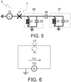
- Figure 5 illustrates an electrical equivalent diagram of an embodiment of the quantum system 1 of figure 3 which takes the form of a capacitive circuit.
- injection locking is ignored here, and the microwave source 15 is not taken into account.
- injection locking as well as the means to implement it, will only be mentioned and discussed in detail below, in part E.4 and with reference to figure 9 .
- the linear microwave network b/a also includes a first resonant portion 27 and a second resonant portion 29.
- first resonant portion 27 still confers the first mode a having the resonant frequency f a to the non-linear superconducting quantum circuit 3
- second resonant portion 29 confers the second mode b having the resonant frequency f b to the non-linear superconducting quantum circuit 3.
- the first resonant portion 27 still includes a capacitive element 31 and an inductive element 33 while the second resonant portion 29 still includes a capacitive element 35 and an inductive element 37.
- first resonant portion 27 is strongly capacitively coupled to the Josephson junction 17 through a capacitive element 39, whereas the second resonant portion 29 is galvanically coupled to the Josephson junction 17.
- the capacitive element 39 and the short electrically conducting portion connecting respectively the first resonant portion 27 and the second resonant portion 29 to the Josephson junction 17 correspond to the linear coupler 19 of figure 3 .
- the second resonant portion 29 can also be capacitively coupled to the Josephson junction 17, whether the first resonant portion 27 and the Josephson junction 17 are galvanically or capacitively coupled.
- the DC voltage source 13 is used to perform the 2-to-1 photon conversion. More particularly, as illustrated in figures 3, 4 and 5 , the DC voltage source 13 delivers DC voltage to bias the non-linear element 7 which takes the form of a single Josephson junction 17.
- Figure 6 shows a simplified circuit in which a DC voltage source and a Josephson junction are connected in series.
- the first resonant portion 27 and the second resonant portion 29 which respectively host the first mode a and the second mode b are absent from this circuit in order to only illustrate the interaction between a DC voltage source and a Josephson junction.
- the DC voltage source is denoted 13 while the Josephson junction is denoted 17.
- the DC voltage source 13 delivers a constant voltage V DC across the Josephson junction 17. Furthermore, the phase of the Josephson junction 17 is denoted ⁇ J .
- the DC voltage source 13 is ideal. By “ideal”, it is meant here that the operation of the DC voltage source 13 does not generate voltage noise.
- An ideal DC voltage source can itself be made with a Josephson junction.
- the Cooper pairs also known as BCS pairs (Bardeen-Cooper-Schrieffer pairs) -, which are pairs of electrons bound together at low temperatures, travel the circuit with an energy equal to 2eV DC , where e is the elementary charge.
- phase ⁇ J thus varies linearly with time.
- the non-linear superconducting quantum circuit 3 of the quantum system 1 further comprises the first resonant portion 27 and the second resonant portion 29, and more particularly the first mode a and the second mode b, in addition to the Josephson junction 17.
- the zero-point phase fluctuation of the first mode a is denoted ⁇ a while the zero-point phase fluctuation of the second mode b is denoted ⁇ b .
- the DC voltage source 13 is arranged to deliver DC voltage to bias the Josephson junction 17.
- the DC voltage source 13 is intended to perform the 2-to-1 photon conversion which is usually obtained with parametric pumping at a frequency
- V DC 2 f a ⁇ f b h 2 e
- H DC ⁇ a a ⁇ a + ⁇ b b ⁇ b ⁇ E J cos ⁇ J + ⁇ d t b + b ⁇
- H DC ⁇ a a ⁇ a + ⁇ b b ⁇ b ⁇ E J cos ⁇ DC t + ⁇ a a + a ⁇ + ⁇ b b + b ⁇ + ⁇ d t b + b ⁇
- H DC ⁇ a a ⁇ a + ⁇ b b ⁇ b ⁇ E J cos ⁇ DC t cos ⁇ a a + a ⁇ + ⁇ b b + b ⁇ + E J sin ⁇ DC t sin ⁇ a a + a ⁇ + ⁇ b b + b ⁇ + ⁇ d t b + b ⁇
- H DC RWA ⁇ g 2 ⁇ a 2 b ⁇ + h . c .
- the non-linear element 7 is formed by a single Josephson junction 17.
- the non-linear element 7 may also include a plurality of Josephson junctions.
- figure 7 shows an electrical equivalent diagram of an embodiment of the quantum system 1 similar to that of figure 4 except that the non-linear element 7 comprises three Josephson junctions, i.e. the Josephson junction 17 - the only one present in figure 4 - as well as two additional Josephson junctions 41 and 43.
- the value V DC of the DC voltage delivered by the DC voltage source 13 must be increased since the potential difference generated by the DC voltage source 13 is distributed between the three Josephson junctions 17, 41 et 43.
- Figure 8 illustrates a theoretical comparison between the prior art quantum system 101 and the proposed quantum system 1 with regard to the dissipation of photons over time.
- the lower curve (ATS) corresponds to parametric dissipative stabilization while the upper curve (DC) corresponds to DC cat qubit stabilization.
- the DC voltage source 13 is considered as an ideal DC voltage source. However, in the following, it is now considered that the DC voltage source 13 is not an ideal DC voltage source. In such a case, it is well known to the skilled person that the DC voltage source 13 is accompanied by non-trivial DC voltage noise.
- This drifting phase angle may be tracked and calibrated for via a feedback mechanism.
- the DC voltage source 13 applied to the Josephson junction 17 can be considered as an oscillator since the DC voltage V DC delivered by the DC voltage source 13 is converted into angular frequency ⁇ DC in the microwave environment set-up by the Josephson junction 17. Since the DC voltage V DC delivered by the DC voltage source 13 is disturbed, it is the same for the angular frequency ⁇ DC of the induced microwave oscillation. Injection locking consists of disturbing a first oscillator with a second oscillator operating at a frequency arbitrarily close to that of the first oscillator; strong coupling allows the second oscillator to capture the first oscillator and cause it to have an identical frequency.
- the command circuit 5 further includes a microwave source 15.
- the principle is to use an external signal to lock the phase ⁇ J of the Josephson junction 17.
- the DC voltage source 13 plays the role of the first oscillator while the microwave source 15 plays the role of the second oscillator.
- Figure 9 shows how injection locking can be implemented with the microwave source 15 and a resistive element 45 which are both coupled to the DC voltage source 13.
- injection locking is incorporated into the galvanic circuit of figure 4 .
- the resistive element 45, the DC voltage source 13 and the microwave source 15 are connected in series.
- ⁇ J t ⁇ DC t + ⁇ J 0 ⁇ ⁇ 0 sin ⁇ J + ⁇ L cos ⁇ L t
- - ⁇ J 0 is the initial value of the phase through the Josephson junction
- the resistive element 45 enables, in combination with the DC voltage delivered by the DC voltage source 13 and the injection signal generated by the microwave source 15, low-frequency oscillations to access the nonlinear regime.
- phase-locked regions for any value of the amplitude ⁇ L of the injection signal, i.e. angular frequency ranges around ⁇ DC in which the angular frequency ⁇ J of the Josephson junction 17 is substantially equal to the angular frequency ⁇ L of the injection signal.
- phase-locked regions take the form of so-called Arnold tongues.
- the so-called detuning v
- the previous criterion can be written as follows with the frequencies f DC and f L instead of the respective angular frequencies ⁇ DC and ⁇ L : f DC ⁇ f L ⁇ ⁇ L ⁇ 0 4 ⁇
- the curve of figure 10 can also be obtained equivalently by varying the angular frequency ⁇ L of the injection signal instead of the angular frequency ⁇ DC of the induced microwave oscillation since the principle is to vary the detuning v.
- the quantity ⁇ J ⁇ ⁇ L 2 ⁇ is substantially equal to 0 GHz.
- the frequency f L of the injection signal is comprised in the range [ f Dc - 0.005; f DC + 0.005]
- the angular frequency ⁇ J of the Josephson junction 17 is substantially equal to the angular frequency ⁇ L of the injection signal.
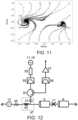
- Figure 11 illustrates the stabilization of the phase of the cat qubit obtained thanks to injection locking.
- figure 12 illustrates an experimental circuit for realizing the quantum system 1.
- This experimental circuit includes the first mode a and the second mode b coupled by only one Josephson junction 17.
- the microwave source 11 is arranged to deliver microwave radiation at a frequency substantially equal to the second resonant frequency f b to drive the second mode b; and the DC voltage source 13 is arranged to bias the Josephson junction 17 to implement the non-linear conversion between two photons of the first mode a and one photon of the second mode b.
- the DC voltage source 13 is coupled to the resistive element 45 for the purpose of implementing injection locking.
- the experimental circuit further includes the microwave source 15.
- the resistive element 45 is off-chip, i.e. is not part of the non-linear superconducting quantum circuit 3.
- the resistive element 45 is part of the command circuit 5.
- the resistive element 45 can be incorporated within the superconducting quantum circuit 3, and more particularly in the non-linear element 7, in the first resonant portion 27 or in the second resonant portion 29. In such a case, the resistive element 45 is on-chip.
- the experimental circuit further includes a bias-tee 47 which is a diplexer, and thus allows two ports - the AC and DC signals respectively delivered by the DC voltage source 13 and the microwave source 11 or the microwave source 15.
- the bias-tee 47 includes an inductive element 49 and a capacitive element 51.
- the experimental circuit also includes an attenuator 53 for selectively attenuating signals delivered by the microwave source 11 or the microwave source 15, and a high-frequency (HF) filter 55 arranged to filter signals that do not belong to the desired frequency band.
- the HF filter 55 may for instance correspond to the microwave filter 25 in figure 3 .
- a high-frequency-mobility transistor (HEMT) 57 is arranged to amplify the signal for the purpose of readout, and a HF filter 59 is coupled to the HEMT 57.
- a circulator 61 is arranged to enable unidirectional signal flow, and thus prevents the entering signal to "bounce" back.
- a DC filter can be added to the experimental circuit in order to filter parasitic high frequency noise originating from the DC voltage source 13.
- a voltage divider can also be used to divide the input voltage and thus reduces the input voltage noise.
- the bias-tee 47 is a diplexer, which enables two input ports or lines carrying signals to be multiplexed into a third line without the signals carried by the two input lines interfering with each other. Namely the DC signal from the DC voltage source 13 and the AC signal from the microwave source 11 or the microwave source 15 are multiplexed into a single output line of the bias-tee 47.
Landscapes
- Engineering & Computer Science (AREA)
- General Physics & Mathematics (AREA)
- Theoretical Computer Science (AREA)
- Physics & Mathematics (AREA)
- Mathematical Analysis (AREA)
- Data Mining & Analysis (AREA)
- Evolutionary Computation (AREA)
- Condensed Matter Physics & Semiconductors (AREA)
- Computational Mathematics (AREA)
- Mathematical Optimization (AREA)
- Pure & Applied Mathematics (AREA)
- Computing Systems (AREA)
- General Engineering & Computer Science (AREA)
- Mathematical Physics (AREA)
- Software Systems (AREA)
- Artificial Intelligence (AREA)
- Superconductor Devices And Manufacturing Methods Thereof (AREA)
Abstract
- a command circuit (5) including a microwave source (11) and a DC voltage source (13), and
- a non-linear superconducting quantum circuit (3) including a non-linear element (7) comprising a Josephson junction, a first and a second resonant portions respectively having a first mode with a first resonant frequency fa and a second mode with a second resonant frequency fb.
• the microwave source (11) delivers microwave radiation at a frequency equal to fb to the second resonant portion to drive the second mode, and
• the DC voltage source (13) delivers DC voltage to bias the non-linear element (7), with the delivered DC voltage having a value inducing a microwave oscillation having a frequency equal to |2fa - fb |.
Description
- The field of the invention relates to stabilizing a cat qubit.
- Generally speaking, superconducting qubits can be implemented as two-level systems of superconducting electronic circuits. Such qubits can be stored in bosonic modes and thus form a particular class of superconducting qubits known as bosonic qubits.
- It is known from the state of the art that it is possible to stabilize cat qubits, i.e. bosonic qubits defined by a quantum manifold spanned by the superpositions of two coherent states, which are quasi-classical states of the bosonic mode. To this end, a specific dissipative stabilization mechanism may be performed and consists in engineering a non-linear conversion between two photons of a first mode - also known as memory mode or cat qubit mode - that hosts the stabilized quantum manifold and one photon of a second mode - also known as buffer mode - that is strongly dissipative.
- The possibility of realizing such a qubit has been demonstrated by R. Lescanne et al. in "Exponential suppression of bit flips in a qubit encoded in an oscillator" (Nature Physics, 2020). As above-mentioned, the cat qubits rely on a mechanism that dissipates photons in pairs. This process pins down two coherent states to separate locations in phase space. By increasing this separation, an exponential decrease of the bit-flip rate was observed experimentally while only linearly increasing the phase-flip rate. As a result, stabilized cat qubits were demonstrated to benefit from a high noise bias, which means that the bit-flip probability is exponentially smaller than the phase-flip probability. Specifically, this was achieved by using an asymmetrical threaded superconducting quantum interference device ("ATS") as a four-wave mixing non-linear element to engineer the 2-to-1 photon conversion.
- Such a 2-to-1 photon conversion is implemented by means of a parametric pump at frequency |2fa - fb |, where fa is the resonant frequency of the memory mode and fb is the resonant frequency of the buffer mode. However, in such a case, the corresponding two-photon coupling rate g 2, which quantifies the strength of the 2-to-1 photon conversion, is proportional to the amplitude εp of the parametric pump. Consequently, the two-photon coupling rate g 2 is limited by the amplitude εp of the parametric pump. That is, the Applicant has recognized that the amplitude of the parametric pump used in the prior art to enable four-wave mixing via the non-linear element cannot be arbitrarily increased without introducing parasitic effects associated with the harmonics of this AC pump (i.e. mixing of the pump into higher order non-linear terms may eventually produce undesirable effects).
- The present invention seeks to improve the situation.
- To this end, the invention relates to a quantum system for stabilizing a cat qubit comprising:
- a command circuit including a microwave source for delivering microwave radiation and a DC voltage source for delivering DC voltage, and
- a non-linear superconducting quantum circuit including a non-linear element, the non-linear element including at least one Josephson junction, a first resonant portion having a first mode with a first resonant frequency and a second resonant portion having a second mode with a second resonant frequency, the non-linear element being coupled to the first resonant portion and the second resonant portion.
- The quantum system is arranged such that, when
- the microwave source delivers microwave radiation at a frequency substantially equal to the second resonant frequency to the second resonant portion to drive the second mode, and
- the DC voltage source delivers DC voltage to bias the non-linear element, with the delivered DC voltage having a value inducing a microwave oscillation having a frequency substantially equal to the absolute value of the difference between twice the first resonant frequency and the second resonant frequency in the non-linear superconducting quantum circuit,
- According to one or more embodiments, the DC voltage source is an ideal DC voltage source.
- According to one or more embodiments, the quantum system comprises a resistive element coupled to the DC voltage source, and the command circuit comprises an additional microwave source arranged to deliver to the DC voltage source microwave radiation at a frequency derived from the frequency of the microwave oscillation induced by the DC voltage source to cause injection locking thereof.
- The resistive element can be incorporated within the non-linear superconducting quantum circuit. In such a case, the resistive element is "on-chip".
- Alternatively, the resistive element can be incorporated within the command circuit. In such a case, the resistive element is "off-chip".
- Preferably, the additional microwave source is arranged to deliver microwave radiation at a frequency fL satisfying the condition


- According to one or more embodiments, the non-linear element includes only one Josephson junction, and the DC voltage source is arranged to deliver DC voltage having a value VDC verifying

- Alternatively, the non-linear element includes a plurality of Josephson junctions, and the DC voltage source is arranged to deliver DC voltage having a value VDC verifying VDC =

- According to one or more embodiments, the non-linear element is galvanically coupled to the first resonant portion.
- Alternatively, the non-linear element is capacitively coupled to the first resonant portion.
- According to one or more embodiments, the non-linear element is galvanically coupled to the second resonant portion.
- Alternatively, the non-linear element is capacitively coupled to the second resonant portion.
- Furthermore, the invention also relates to a method for stabilizing a cat qubit implemented by the quantum system described above and comprising the following operations:
- delivering, by the microwave source, microwave radiation at a frequency substantially equal to the second resonant frequency to the second resonant portion to drive the second mode, and
- delivering, by the DC voltage source, DC voltage to bias the non-linear element, with the delivered DC voltage having a value inducing a microwave oscillation having a frequency substantially equal to the absolute value of the difference between twice the first resonant frequency and the second resonant frequency in the non-linear superconducting quantum circuit.
- Other features and advantages of the invention will become apparent from the following description provided for indicative and non-limiting purposes, with reference to the accompanying drawings, wherein:
-
Figure 1 illustrates a prior art quantum system for stabilizing a cat qubit by implementing a parametric dissipative stabilization, -
Figure 2 schematically illustrates a quantum system according to the invention, -
Figure 3 illustrates an explicit diagram of the quantum system offigure 2 , -
Figure 4 illustrates a partial electrical equivalent diagram of a galvanic example implementation of the quantum system offigure 3 , -
Figure 5 illustrates a partial electrical equivalent diagram of a capacitive example implementation of the quantum system offigure 3 , -
Figure 6 illustrates a circuit including a DC voltage source applied across a Josephson junction, -
Figure 7 illustrates a variant of the galvanic example implementation offigure 4 in which the non-linear element includes three Josephson junctions, -
Figure 8 illustrates a theoretical comparison of the time evolution of photon dissipation for the prior art quantum system offigure 1 and the quantum system according to the present invention, -
Figure 9 illustrates a variant of the galvanic example implementation offigure 4 in which a microwave source and a resistive element are provided for implementing injection locking, -
Figure 10 illustrates the influence of the amplitude of the injection locking pump on the stabilization of the frequency of the Josephson junction, -
Figure 11 illustrates how injection locking contributes to the stabilization of the phase of the cat qubit, and -
Figure 12 illustrates an experimental circuit for realizing the quantum system according to the invention with injection locking. - The drawings and the following description are comprised for the most part of positive and well-defined features. As a result, they are not only useful in understanding the invention, but they can also be used to contribute to its definition, should the need arise.
- So far, the Applicant's work has been generally concerned with the stabilization of cat qubits. As previously explained, R. Lescanne et al. (2020) demonstrated that such cat qubits can be stabilized with a non-linear conversion between two photons of a first mode a - memory mode or cat qubit mode - and one photon of a second mode b - buffer mode.
- A cat qubit is defined as a two-dimensional manifold spanned by the so-called cat states


- Stabilized cat qubits are known to benefit from a high noise bias, which means that the bit-flip probability is exponentially smaller than the phase-flip probability. More precisely, an effective error channel (e.g., bit errors or "bit-flips") is suppressed in an exponential way with the "size" - i.e. the average number of photons
n = |α|2 - of the Schrödinger cat states of the cat qubits. As previously mentioned, this exponential suppression of bit-flip errors is only at the cost of linear increase of phase-flip errors. - According to current knowledge, this suppression should apply to a large class of physical noise processes having a local effect on the phase space of a harmonic oscillator. This includes, but is not limited to, photon loss, thermal excitations, photon dephasing, and various nonlinearities induced by coupling to a Josephson junction.
- Recent experiments in the context of quantum superconducting circuits have observed this exponential suppression of bit-flip errors with the average number of photons in the cat states.
- It is generally considered that the use of a single repetition code is sufficient to correct the remaining errors as bit-flip errors are sufficiently rare; and, more particularly, a phase-flip error correction code is sufficient to correct the remaining phase-flip. This can be for instance a repetition code defined in the dual base or any other state-of-the-art error correction code.
- The cat qubits can be stabilized or confined by the following exemplary schemes:
- a) a parametric dissipative stabilization, with
jump operator 

- b) a Kerr Hamiltonian

- c) a detuned Kerr Hamiltonian

- d) a two-photon exchange (TPE) Hamiltonian

- e) a dissipative squeezing stabilization, with jump operator


- f) a variant of the previous stabilization scheme e), for which the Applicant filed the European patent application
EP 23175147.0 
- g) a resonant dissipative stabilization, with
jump operator 

- The present invention aims to implement stabilization in the spirit of parametric dissipative stabilization according to scheme a) or d).
- The parametric dissipative stabilization relies on generating the following terms:
- a 2 b † + h. c. : this first term corresponds to the non-linear conversion between two photons of a first mode a - the memory - and one photon of a second mode b - the buffer. This term requires a pump at a frequency |2fa - fb |, where fa is the resonant frequency of the first mode a and fb is the resonant frequency of the second mode b. Such a pump is thus a two-photon pump.
- α 2 b † + h. c.: this second term requires the drive of the second mode b at a frequency fb. Such a drive, referred to as buffer drive, combined with the previous conversion terms effectively becomes a two-photon drive.
- For this purpose, it is known to the skilled person that the first mode a and the second mode b can be coupled via an ATS, and to generate the first term using a microwave source arranged to deliver radiation at a frequency substantially equal frequency to |2fa - fb | to parametrically drive the ATS.
- However, as detailed below, such an implementation of the 2-to-1 photon conversion has the disadvantage that the two-photon coupling rate g 2 is proportional to the amplitude εp of the microwave source - or two-photon pump. Consequently, the constraints on the amplitude εp limit the value of the two-photon coupling rate g 2 accordingly, i.e. the amplitude εp cannot be arbitrarily increased - for increasing the strength of the 2-to-1 photon conversion - without introducing parasitic effects associated with the harmonics of this AC parametric drive (i.e. mixing of the AC drive into higher order non-linear terms may eventually produce undesirable effects).
- The present invention presents an alternative to the use of a microwave source to carry out the 2-to-1 photon conversion in order to obtain a higher two-photon coupling rate g 2 .
-
Figure 1 illustrates a priorart quantum system 101 for implementing a parametric dissipative stabilization. - The
quantum system 101 comprises a non-linear superconductingquantum circuit 103 and acommand circuit 105. - The non-linear superconducting
quantum circuit 103 is arranged to make possible four-wave mixing between the first mode a and the second mode b. - The non-linear superconducting
quantum circuit 103 is intended to be subject to microwave radiations delivered by thecommand circuit 105 in order to engineer various non-linear interactions between the first mode a and the second mode b. The frequency of each microwave radiation is tuned to select specific terms within the rotating-wave approximation. - The non-linear superconducting
quantum circuit 103 comprises anon-linear element 107 and at least oneresonant portion 109. - The
non-linear element 107 is arranged to engineer the first term a 2 b † + h. c. of the jump operator L 2 for stabilizing the cat qubit. - The
non-linear element 107 is an ATS. It is known to the skilled person that an ATS can be used to engineer the 2-to-1 photon conversion, i.e. the first term a 2 b † of the jump operator L 2, in order to perform a parametric dissipative stabilization, as successfully shown by R. Lescanne et al. (2020). More particularly, such a 2-to-1 photon conversion between the first mode a and the second mode b is obtained by parametrically pumping the ATS at the frequency fp = |2fa - fb |. Advantageously, the pump frequency satisfies fp ≫ g 2 to make this parametric pumping work as well as possible. - Contrary to the first implementations of this stabilization scheme proposed by Z. Leghtas et al. (2015) and S. Touzard et al. (2018) in which the superconducting circuit element used as a four-wave mixer was a transmon with a single Josephson junction, the solution developed by R. Lescanne et al. (2020) exploits the ATS design which has much lower cross-Kerr terms than the transmon and thus allowed to observe the exponential suppression of bit-flips.
- It is known to the skilled person that, when biased at its flux working point (0 - π or conversely), the Hamiltonian HATS of the
ATS 107 has the following "sin-sin" form:
ATS 107, φa is the zero-point fluctuation of the phase of the first mode a across theATS 107 and φb is the zero-point fluctuation of the phase of the second mode b across theATS 107, EJ is the Josephson energy of the side junctions and EL is the inductive energy of a central inductance, φ Σ(t) corresponds to a common flux modulation of the two loops of theATS 107 and φ Δ(t) corresponds to a differential flux modulation of the two loops of theATS 107. The former can be implemented by delivering microwave radiations through flux lines of theATS 107 out of phase, the latter can be implemented by delivering microwave radiations through flux lines of theATS 107 in phase. - Parametric pumping of the
ATS 107 is typically done by pumping the common flux as pumping the differential flux merely displaces the modes coupled to theATS 107. As an example, by pumping the common flux at the frequency fp = |2fa - fb |, φΣ (t) = εp cos (2πfpt), the non-linear resonant part of the Hamiltonian writes in the rotating frame:
- The
resonant portion 109 is arranged to be connected to theATS 107 to provide the non-linear superconductingquantum circuit 103 with the first mode a and the second mode b having respective resonant frequencies fa and fb. The participation of the first mode a in theATS 107 is quantified by the zero-point fluctuation φa, while the participation of the second mode b in theATS 107 is quantified by the zero-point fluctuation φb. - The
resonant portion 109 is a linear microwave network b/a. Such a linear microwave network b/a is such that, when coupled via alinear coupler 119 to theATS 107 which acts as an inductive element, the non-linear superconductingquantum circuit 103 has the first mode a and the second mode b at respective resonant frequencies fa and fb which participate in theATS 107. - The
command circuit 105 is arranged to deliver microwave radiations. To this end, as illustrated infigure 1 , thecommand circuit 105 comprises at least amicrowave source 111 and amicrowave source 127. - The
microwave source 127 is set-up to modulate the common flux in theATS 107. More particularly, themicrowave source 127 is arranged to deliver microwave radiations through flux lines of theATS 107 out of phase to implement the common flux modulation φΣ (t). - For this purpose, a microwave network 129 is used to split the radiation emitted by the
microwave source 127 and apply it to each node of theATS 107 with the correct phase. Alternatively, two different microwave sources could be used, each being simply coupled to a single node of theATS 107 and their relative phase and amplitude being set so as to achieve the desired flux modulation. - When the
microwave source 127 is set at the frequency |2fa - fb |, the non-linear superconductingquantum circuit 103 performs the 2-to-1 photon conversion between the first mode a and the second mode b. To convert this 2-to-1 photon conversion into two-photon dissipation, the second mode b is selectively coupled to aload 121 via alinear coupler 123 and a microwave filter 125 configured as a band pass filter with a frequency fb. - Alternatively, the microwave filter 125 may be configured as a band stop filter at a frequency fa and may be placed in between, on the one hand, the external environment and, on the other hand, the first mode a and the second mode b to isolate the first mode a and thus prevent the first mode a from suffering additional losses coming from unwanted coupling to the
load 121. - Alternatively, it may be configured as a low-pass (respectively high-pass) filter if fa > fb (resp fb > fa ). In other embodiments, the microwave filter 125 can be omitted when coupling between the
load 121 and substantially only the second mode b can be established. The skilled person thus understands that the first mode a has a high-quality factor while the second mode b has a low-quality factor. - The
microwave source 111 is arranged to drive the second mode b in order to engineer the second term α2b † + h. c. of the jump operator L 2 for stabilizing the cat qubit. As previously explained, themicrowave source 111 is thus arranged to deliver microwave radiation at a frequency substantially equal to fb to the linear microwave network b/a. - In the above, the
load 121 can be seen as part of thecommand circuit 105 offigure 1 , while thelinear coupler 123 and the microwave filter 125 can be seen as part of the non-linear superconductingquantum circuit 103. - Finally, in
figure 1 , thecommand circuit 105 further comprises amicrowave source 131 set-up to modulate the differential flux in theATS 107 through the microwave network 129. More particularly, themicrowave source 131 is arranged to deliver microwave radiations through flux lines of theATS 107 in phase to implement the differential flux modulation φ Δ(t). - It is to be noted that the microwave network 129 is used for convenience but can be omitted and the
microwave source 131 could be applied directly to both nodes of theATS 107, their relative phase and amplitude being set so as to achieve the desired flux modulation. - For the sake of completeness, it may also be noted that the
microwave source 131 can be used, instead of themicrowave source 111, to deliver microwave radiation at a frequency fb to the linear microwave network b/a to drive the second mode b. - As above-mentioned, the parametric dissipative stabilization implemented using an ATS as well as a two-photon pump at a frequency |2fa - fb | to parametrically pump the ATS results in a two-photon coupling rate g 2 which is proportional to the amplitude εp of the microwave source used as two-photon pump.
- Referring again to
figure 1 , themicrowave source 111 delivers microwave radiation at a frequency fd substantially equal to fb to drive the second mode b. Such a buffer drive can be expressed as follows:
- The
microwave source 127 delivers microwave radiation at a frequency fp substantially equal to |2fa - fb | to parametrically drive theATS 107. Such a two-photon pump can be expressed as follows:
- The "sin-sin" form of the Hamiltonian HATS of the
ATS 107 can be written as follows:
- In order to avoid strong pump effect, the two-photon pump is carried out such that the amplitude εp is very small compared to 1: εp ≪ 1. Consequently, it is possible to neglect the higher order terms in the sine expansion:


- The Hamiltonian HATS can be written as follows within the rotating-wave approximation:

- Consequently:

- Consequently, in the limit of small pump amplitude, the two-photon coupling rate g 2 is proportional to the amplitude εp of the two-photon pump:
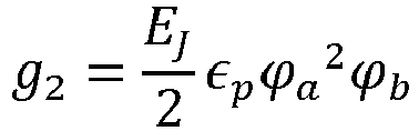
- Due to this linear dependence, the two-photon exchange interaction is determined by the amplitude εp of the two-photon pump.
- A known solution to avoid such a limitation is to implement a resonant dissipative stabilization which corresponds to the previous stabilization scheme g).
- The resonant dissipative stabilization corresponds to the particular case where 2fa = fb, and therefore where the 2-to-1 photon conversion is not activated by parametric pumping. Consequently, only the drive of the second mode b at a frequency fb is necessary to engineer the jump operator L2.
- The resonant case, where fp = 0, may be particularly advantageous, as developed in the European patent application
EP 21306965.1 - On the other hand, one benefit of the above-detailed four-wave mixing non-linear element is that the two-to-one photon exchange can be easily switched off, which may be beneficial for particular operations such as a CNOT gate. Moreover, such a four-wave mixing non-linear element makes it possible to avoid the spurious cross-Kerr terms and the related additional noise which caused recurring issues in the very first implementations, i.e. Z. Leghtas et al. (2015) and S. Touzard et al. (2018), of the above-detailed stabilization scheme due to the presence of a transmon.
- The Applicant has therefore recognized that it may be advantageous to use an alternative four-wave mixing mechanism which does not rely on a two-photon AC pump, and thus may thereby avoid parasitic effects associated with harmonics of the two-photon AC pump, whilst still remaining easy to switch off.
- The Applicant thus proposes the
quantum system 1 schematically illustrated infigure 2 . A detailed architecture of thequantum system 1 and its advantages compared to parametric dissipative stabilization are developed below. -
Figure 2 illustrates aquantum system 1 comprising a non-linear superconductingquantum circuit 3 and acommand circuit 5. - The non-linear superconducting
quantum circuit 3 is arranged to make possible four-wave mixing between a first mode a and a second mode b. In the following, the first mode a is used as a memory hosting a cat qubit, while the second mode b is used as a buffer in between the cat qubit and the external environment. - The first mode a and the second mode b each correspond to natural resonant frequencies of the non-linear superconducting
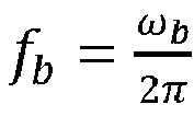
quantum circuit 3. Consequently, the first mode a and the second mode b each have a respective resonant frequency. The first mode a has a resonant frequency
- By "having" a first mode and a second mode, it should be understood here that the non-linear superconducting
quantum circuit 3 comprises components operating in a superconducting regime which host the modes independently of each other or concurrently. In other words, the first mode a and the second mode b may be hosted in different subsets of components of the superconducting circuit or on the same subset of components. - The first mode a has a high-quality factor Qa while the second mode b has a low-quality factor Qb. As will be appreciated, the quality factor (Q-factor) can be determined in various ways, for instance by: (a) spectroscopic linewidth measurement, wherein the quality factor is given by Q = f/Δf, wherein f is resonant frequency and Δf is the spectroscopic linewidth; or (b) via a time-domain measurement wherein a tone is sent in, and a return signal is measured after a pre-determined time, wherein Q = f * τ with τ the characteristic decay time. Of course, the skilled person would be aware of various other methods for determining the quality factor of a particular mode.
- In the context of the invention, the second mode b is more dissipative than the first mode a. In particular, the first mode a has a high-quality factor Qa while the second mode b has a low-quality factor Qb. A high-quality factor Qa means that the rate at which photons are lost from the first mode a directly to the environment is much lower - typically 106 times lower - than the resonant frequency fa . Furthermore, for the purpose of stabilizing a cat qubit, the energy leak rate κb of the second mode b defined as


- In practice, the Applicant has observed that the energy leak rate κa of the first mode a is preferably five times smaller than the quantity


- The invention thus falls within a different framework than implementations such as, for instance, the design of a bright source of entangled microwaves. Indeed, such an implementation requires, inter alia, that the respective energy leak rates κa and κb of the first mode a and the first mode b be similar, as well as the respective quality factors Qa et Qb of the first mode a and the first mode b, or even that the quality factor Qb of the second mode b is greater than the quality factor Qa of the first mode a. Conversely, here, the quality factor Qa of the first mode a is significantly greater than the quality factor Qb of mode b.
- The ratio of the quality factor of the first mode a to the second mode b (Qa /Qb) may be greater than 100. Preferably the ratio Qa /Qb is greater than 1000, more preferably greater than 10,000.
- The non-linear superconducting
quantum circuit 3 is intended to be subject to microwave radiation and DC voltage both delivered by thecommand circuit 5 in order to engineer various non-linear interactions between the first mode a and the second mode b. - The non-linear superconducting
quantum circuit 3 comprises anon-linear element 7 and anassembly 9 of two or more resonant portions. In the following and for the sake of conciseness, theassembly 9 includes two resonant portions : a first resonant portion and a second resonant portion ; even if theassembly 9 can include more than two resonant portions. - The
non-linear element 7 is arranged to engineer a Hamiltonian HDC for stabilizing a cat qubit. The expression of such a Hamiltonian HDC will be detailed hereinafter. - In the context of the present invention, the
non-linear element 7 only includes one or more Josephson junctions to generate the parametric frequency |2fa - fb | via a DC bias, rather than, e.g., an ATS driven by a parametric pump. - The
assembly 9 of two resonant portions is arranged to be coupled or connected to thenon-linear element 7 to provide the non-linear superconductingquantum circuit 3 with the first mode a and the second mode b having respective resonant frequencies fa and fb. More particularly, the first mode a and the second mode b "participate" in thenon-linear element 7, which means that a portion or the entirety of the mode magnetic energy is stored in thenon-linear element 7. Such a participation can be quantified by the zero-point fluctuation of the superconducting phase across the one or more Josephson junctions, noted φa for the first mode a and φb for the second mode b. The first mode a and the second mode b correspond to electromagnetic modes, i.e. a cat qubit mode and a buffer mode respectively. - The
command circuit 5 is arranged to deliver microwave radiations and DC voltage to cause thenon-linear element 7 to engineer the Hamiltonian HDC for stabilizing the cat qubit. - To this end, and as illustrated in
figure 2 , the command circuit comprises afirst microwave source 11, aDC voltage source 13 and asecond microwave source 15. - The
first microwave source 11 is arranged to drive the second mode b by delivering microwave radiation at a frequency substantially equal to the second resonant frequency fb to theassembly 9 of two resonant portions. Such a drive corresponds to the so-called buffer drive. - The
DC voltage source 13, which therefore replaces here the microwave source usually used to implement the non-linear conversion between two photons of the first mode a and one photon of the second mode b, is arranged to bias thenon-linear element 7 with the delivered DC voltage having a value inducing a microwave oscillation having a frequency substantially equal to |2fa - fb | in the non-linear superconductingquantum circuit 3. - Finally, the second - or additional -
microwave source 15 is arranged to deliver microwave radiation at a frequency substantially equal to the frequency of the microwave oscillation induced by theDC voltage source 13 to cause injection locking thereof. As explained below, such an injection locking is particularly useful when theDC voltage source 13 is not an ideal DC voltage source, i.e. when theDC voltage source 13 induces voltage noise. -
Figure 3 shows a detailed architecture of thequantum system 1 for implementing a dissipative stabilization. - The
non-linear element 7 is a set of one or more Josephson junctions to which theassembly 9 of two resonant portions, which is a linear microwave network b/a, is connected. In the example described here, thenon-linear element 7 includes only oneJosephson junction 17. - The linear microwave network b/a can be compared to that of the prior
art quantum system 101 illustrated infigure 1 and is such that, when coupled via alinear coupler 19 to thenon-linear element 7, the non-linear superconductingquantum circuit 3 has the first mode a and the second mode b at respective resonant frequencies fa and fb which participate in thenon-linear element 7. - Similarly to the prior
art quantum system 101, the microwave source 11 - that can be compared to the microwave source 111 - is arranged to drive the second mode b at the second resonant frequency fb. - More particularly, the second mode b is selectively coupled to a
load 21 via alinear coupler 23 and amicrowave filter 25 configured as a band pass filter with a frequency fb. - Again, the
microwave filter 25 may be configured as a band stop filter at a frequency fa and may be placed in between, on the one hand, the external environment and, on the other hand, the first mode a and the second mode b to isolate the first mode a and thus prevent the first mode a from suffering additional losses coming from unwanted coupling to theload 21. - It may also be configured as a low-pass (respectively high-pass) filter if fa > fb (resp fb > fa ). In other embodiments, the
microwave filter 25 can be omitted when coupling between theload 21 and substantially only the second mode b can be established. The skilled person thus understands that the first mode a has a high-quality factor while the second mode b has a low-quality factor. - The skilled person understands that the
linear coupler 19, theload 21, thelinear coupler 23 and themicrowave filter 25 of thequantum system 1 can be compared respectively to thelinear coupler 119, theload 121, thelinear coupler 123 and the microwave filter 125 of the priorart quantum system 101. - The
command circuit 5 does not comprise anything functionally comparable to themicrowave source 127, the microwave network 129 or themicrowave source 131. Instead, thecommand circuit 5 comprises theDC voltage source 13 and themicrowave source 15 to perform the 2-to-1 photon conversion; such a 2-to-1 photon conversion being converted into a two-photon drive with the drive of the second mode b at frequency fb performed using themicrowave source 11, and into a two-photon dissipation with theload 21. -
Figure 4 illustrates an electrical equivalent diagram of an embodiment of thequantum system 1 offigure 3 which takes the form of a galvanic circuit. - Such an electrical equivalent diagram is partial since it only represents the
non-linear element 7 and the linear microwave network b/a, and thus represent neither thelinear coupler 19 nor themicrowave filter 25. - It should also be noted that the injection locking is ignored here, and therefore that the
microwave source 15 is not taken into account. Injection locking, as well as the means to implement it, will only be mentioned and discussed in detail below, in part E.4 and with reference tofigure 9 . - As in
figure 3 , thenon-linear element 7 comprises only oneJosephson junction 17. - The linear microwave network b/a includes a first
resonant portion 27 and a secondresonant portion 29. - Both the first
resonant portion 27 and the secondresonant portion 29 are galvanically coupled to theJosephson junction 17. The firstresonant portion 27 confers the first mode a having the resonant frequency fa to the non-linear superconductingquantum circuit 3 while the secondresonant portion 29 confers the second mode b having the resonant frequency fb to the non-linear superconductingquantum circuit 3. - By "galvanically coupled", it should be understood here that there are short electrically conducting portions which connect the first
resonant portion 27 and the secondresonant portion 29 to theJosephson junction 17, i.e., a short electrically conducting track or any other mean ensuring a physically continuous conducting junction. The expression "short" means that the electrically conducting track has an impedance which is negligeable compared to the impedance of theJosephson junction 17, the firstresonant portion 27 and the secondresonant portion 29 at the resonant frequencies fa and fb. These short electrically conducting portions correspond to thelinear coupler 19 offigure 3 . - In the embodiment of
figure 4 , the firstresonant portion 27 includes acapacitive element 31 and aninductive element 33 which are connected in parallel. Similarly, the secondresonant portion 29 includes acapacitive element 35 and aninductive element 37 which are connected in parallel. -
Figure 5 illustrates an electrical equivalent diagram of an embodiment of thequantum system 1 offigure 3 which takes the form of a capacitive circuit. - Similarly to
figure 4 , such an electrical equivalent diagram is partial and only represents the non-linear element 7 - which comprises only one Josephson junction 17 - and the linear microwave network b/a. - Once again, the injection locking is ignored here, and the
microwave source 15 is not taken into account. As a reminder, injection locking, as well as the means to implement it, will only be mentioned and discussed in detail below, in part E.4 and with reference tofigure 9 . - The linear microwave network b/a also includes a first
resonant portion 27 and a secondresonant portion 29. For the sake of simplification, the same reference signs are used; the firstresonant portion 27 still confers the first mode a having the resonant frequency fa to the non-linear superconductingquantum circuit 3, while the secondresonant portion 29 confers the second mode b having the resonant frequency fb to the non-linear superconductingquantum circuit 3. - In
figure 5 , the firstresonant portion 27 still includes acapacitive element 31 and aninductive element 33 while the secondresonant portion 29 still includes acapacitive element 35 and aninductive element 37. - It must be noted that the first
resonant portion 27 is strongly capacitively coupled to theJosephson junction 17 through acapacitive element 39, whereas the secondresonant portion 29 is galvanically coupled to theJosephson junction 17. Thecapacitive element 39 and the short electrically conducting portion connecting respectively the firstresonant portion 27 and the secondresonant portion 29 to theJosephson junction 17 correspond to thelinear coupler 19 offigure 3 . - It must also be noted that the second
resonant portion 29 can also be capacitively coupled to theJosephson junction 17, whether the firstresonant portion 27 and theJosephson junction 17 are galvanically or capacitively coupled. - As detailed above, the
DC voltage source 13 is used to perform the 2-to-1 photon conversion. More particularly, as illustrated infigures 3, 4 and5 , theDC voltage source 13 delivers DC voltage to bias thenon-linear element 7 which takes the form of asingle Josephson junction 17. -
Figure 6 shows a simplified circuit in which a DC voltage source and a Josephson junction are connected in series. In this figure, the firstresonant portion 27 and the secondresonant portion 29 which respectively host the first mode a and the second mode b are absent from this circuit in order to only illustrate the interaction between a DC voltage source and a Josephson junction. For the sake of consistency with the rest of the description, the DC voltage source is denoted 13 while the Josephson junction is denoted 17. - The
DC voltage source 13 delivers a constant voltage VDC across theJosephson junction 17. Furthermore, the phase of theJosephson junction 17 is denoted φJ. - At this stage, for simplicity, we can consider that the
DC voltage source 13 is ideal. By "ideal", it is meant here that the operation of theDC voltage source 13 does not generate voltage noise. An ideal DC voltage source can itself be made with a Josephson junction. - The Cooper pairs - also known as BCS pairs (Bardeen-Cooper-Schrieffer pairs) -, which are pairs of electrons bound together at low temperatures, travel the circuit with an energy equal to 2eVDC, where e is the elementary charge.
- In the microwave environment set up by the
Josephson junction 17, such an energy 2eVDc is converted into photons with an angular frequency ω DC equal to
Josephson junction 17 acts as a "voltage-to-frequency converter". - Consequently, the circuit of
figure 6 can be described with the following differential equation:
- Since the DC voltage VDC is constant over the time, the time evolution of the phase φJ can be expressed as follows:

0 is the initial value of the phase φJ, φ J0 = φJ (0). - The phase φJ thus varies linearly with time.
- Nonetheless, the non-linear superconducting
quantum circuit 3 of thequantum system 1 further comprises the firstresonant portion 27 and the secondresonant portion 29, and more particularly the first mode a and the second mode b, in addition to theJosephson junction 17. In the following, the zero-point phase fluctuation of the first mode a is denoted φa while the zero-point phase fluctuation of the second mode b is denoted φb. - As previously explained, the
DC voltage source 13 is arranged to deliver DC voltage to bias theJosephson junction 17. The value VDC of the DC voltage induces a microwave oscillation having an angular frequency ω DC such that
DC voltage source 13 is intended to perform the 2-to-1 photon conversion which is usually obtained with parametric pumping at a frequency |2fa - fb |, the value VDC must be set such that the frequency fDC is equal to |2fa - fb |. - Therefore:

- Then, since the reduced Planck constant λ is defined as


- Then:

- Moreover, the differential equation of the phase φJ of the
Josephson junction 17 must now be expressed as follows:
- The Hamiltonian HDC engineered by the non-linear superconducting
quantum circuit 3, and more particularly by theJosephson junction 17, is expressed as follows:
- Then:

- Then:

- As previously mentioned, the Hamiltonian HDC can be written as follows within the rotating-wave approximation:

- Consequently:

- It thus appears that the two-photon rate g 2 is not determined - and thus limited - by the amplitude of any parametric pump.
- It must be added that the DC voltage delivered by the
DC voltage source 13 leads to a linear increase in the phase across theJosephson junction 17 which averages the Kerr and cross-Kerr terms to zero. - In the examples described so far, the
non-linear element 7 is formed by asingle Josephson junction 17. However, thenon-linear element 7 may also include a plurality of Josephson junctions. - Thus,
figure 7 shows an electrical equivalent diagram of an embodiment of thequantum system 1 similar to that offigure 4 except that thenon-linear element 7 comprises three Josephson junctions, i.e. the Josephson junction 17 - the only one present infigure 4 - as well as twoadditional Josephson junctions - In such a case, the value VDC of the DC voltage delivered by the
DC voltage source 13 must be increased since the potential difference generated by theDC voltage source 13 is distributed between the threeJosephson junctions et 43. In the present case, the value VDC is such that:
- More generally, in the case where the
non-linear element 7 includes N Josephson junctions, where N is a strictly positive natural number, the value VDC of the DC voltage in order to induce a microwave oscillation having a frequency substantially equal to |2fa - fb | in the non-linear superconductingquantum circuit 3 is the following:
-
Figure 8 illustrates a theoretical comparison between the priorart quantum system 101 and the proposedquantum system 1 with regard to the dissipation of photons over time. The lower curve (ATS) corresponds to parametric dissipative stabilization while the upper curve (DC) corresponds to DC cat qubit stabilization. - The lower curve is obtained for an amplitude εp = 0.5 GHz for the parametric pump while the upper curve is obtained for an angular frequency ωDC such that

DC voltage source 13. - More particularly, the comparison was implemented with the following parameters:
-

-

-

- φa = 0.31,
- φb = 0.63, and
- εd = 0.03 GHz.
- It appears that the DC cat qubit stabilization converges more quickly towards the asymptotic limit |α|2 = 3.
- In the respective embodiments of
figures 4 ,5 and7 , theDC voltage source 13 is considered as an ideal DC voltage source. However, in the following, it is now considered that theDC voltage source 13 is not an ideal DC voltage source. In such a case, it is well known to the skilled person that theDC voltage source 13 is accompanied by non-trivial DC voltage noise. Such a charge DC noise can be expressed as a noise voltage δVN (t):
- Consequently, the differential equation of the phase φJ of the
Josephson junction 17 must now be expressed as follows:
- Then:

- The phase φJ of the
Josephson junction 17 can be rewritten as follows:

- Consequently, the two-photon rate g 2 also depends on the DC voltage noise:

- The noise term e iφN (t) reflects that the DC voltage noise induces a time-drifting angle on the first mode a:


- This drifting phase angle may be tracked and calibrated for via a feedback mechanism.
- Additionally or alternatively, in order to overcome this problem, it is possible to implement injection locking to stabilize the phase φJ of the
Josephson junction 17. - As explained previously, the
DC voltage source 13 applied to theJosephson junction 17 can be considered as an oscillator since the DC voltage VDC delivered by theDC voltage source 13 is converted into angular frequency ω DC in the microwave environment set-up by theJosephson junction 17. Since the DC voltage VDC delivered by theDC voltage source 13 is disturbed, it is the same for the angular frequency ωDC of the induced microwave oscillation. Injection locking consists of disturbing a first oscillator with a second oscillator operating at a frequency arbitrarily close to that of the first oscillator; strong coupling allows the second oscillator to capture the first oscillator and cause it to have an identical frequency. - As illustrated in
figures 2 and3 , thecommand circuit 5 further includes amicrowave source 15. The principle is to use an external signal to lock the phase φJ of theJosephson junction 17. In other words, theDC voltage source 13 plays the role of the first oscillator while themicrowave source 15 plays the role of the second oscillator. Themicrowave source 15 thus delivers microwave radiation at an angular frequency ω L , where fL =
microwave source 15. Such microwave radiations can be considered as "injection signal". -
Figure 9 shows how injection locking can be implemented with themicrowave source 15 and aresistive element 45 which are both coupled to theDC voltage source 13. In the example offigure 9 , injection locking is incorporated into the galvanic circuit offigure 4 . Theresistive element 45, theDC voltage source 13 and themicrowave source 15 are connected in series. - The presence of the
resistive element 45 and the injection signal at angular frequency ωL of themicrowave source 15 induce the following equation of the phase φJ of the Josephson junction 17:
0 is the initial value of the phase through the Josephson junction, -

Josephson junction 17 and R 0 is the resistance of the addedresistive element 45 such that ν 0 is the phase contribution of theresistive element 45, and - εL is the amplitude of the
microwave source 15. - As will be appreciated, the
resistive element 45 enables, in combination with the DC voltage delivered by theDC voltage source 13 and the injection signal generated by themicrowave source 15, low-frequency oscillations to access the nonlinear regime. - In the context of the present invention, the Applicant has recognized the existence of phase-locked regions for any value of the amplitude εL of the injection signal, i.e. angular frequency ranges around ω DC in which the angular frequency ωJ of the
Josephson junction 17 is substantially equal to the angular frequency ωL of the injection signal. Such phase-locked regions take the form of so-called Arnold tongues. To this end, the so-called detuning v = |ωDC - ωL | preferably verifies the following criterion:
- Equivalently, the previous criterion can be written as follows with the frequencies fDC and fL instead of the respective angular frequencies ω DC and ωL:

- For instance,
figure 10 shows the evolution of the difference between the angular frequency ωJ of theJosephson junction 17 and the angular frequency ωL of the injection signal as a function of the detuning v for a value of the amplitude εL of the injection signal equal to 0.35 gigahertz (GHz). More specifically,figure 10 shows the evolution of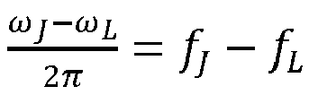

- To be more complete, the curve of
figure 10 was obtained under the following conditions and by varying the angular frequency ωDC of the induced microwave oscillation: -

-

-

- φa = 0.29,
- φb = 0.62,
-

- R 0 = 50 Ω,
- εL = 0.35 GHz,
- εd = 0.05 GHz,
-

- Vnoise = 10.36 nV.
- It must be noted that the curve of
figure 10 can also be obtained equivalently by varying the angular frequency ωL of the injection signal instead of the angular frequency ω DC of the induced microwave oscillation since the principle is to vary the detuning v. In such a case, the condition above

- It appears that, where


Josephson junction 17 is substantially equal to the angular frequency ωL of the injection signal. Preferably, the angular frequency of the injection signal is equal to the angular frequency induced by the DC voltage source, ωL = ωDC. -
Figure 11 illustrates the stabilization of the phase of the cat qubit obtained thanks to injection locking. - Such stabilization was obtained under conditions similar to those of
figure 10 , i.e. with the same values for the parameters listed above, and with:

- This figure shows, in the rotating frame at the frequency memory, semi-classical solutions to the equations of motion of the system showing that with injection locking, two opposite solutions, each taking a spiral shape, are stabilized. As will be appreciated by the skilled person, this is the classical equivalent of a cat state and exemplifies that two photon dissipation to stabilize a cat qubit still works with the injection locking. Without injection locking the steady state would drift in phase in the known reference frame.
- Finally,
figure 12 illustrates an experimental circuit for realizing thequantum system 1. - This experimental circuit includes the first mode a and the second mode b coupled by only one
Josephson junction 17. In addition, themicrowave source 11 is arranged to deliver microwave radiation at a frequency substantially equal to the second resonant frequency fb to drive the second mode b; and theDC voltage source 13 is arranged to bias theJosephson junction 17 to implement the non-linear conversion between two photons of the first mode a and one photon of the second mode b. - The
DC voltage source 13 is coupled to theresistive element 45 for the purpose of implementing injection locking. To this end, the experimental circuit further includes themicrowave source 15. - It must be noted that, in the experimental circuit, the
resistive element 45 is off-chip, i.e. is not part of the non-linear superconductingquantum circuit 3. Here, theresistive element 45 is part of thecommand circuit 5. - However, alternatively, the
resistive element 45 can be incorporated within the superconductingquantum circuit 3, and more particularly in thenon-linear element 7, in the firstresonant portion 27 or in the secondresonant portion 29. In such a case, theresistive element 45 is on-chip. - Still in reference to
figure 12 , the experimental circuit further includes a bias-tee 47 which is a diplexer, and thus allows two ports - the AC and DC signals respectively delivered by theDC voltage source 13 and themicrowave source 11 or themicrowave source 15. Here, the bias-tee 47 includes aninductive element 49 and acapacitive element 51. - The experimental circuit also includes an
attenuator 53 for selectively attenuating signals delivered by themicrowave source 11 or themicrowave source 15, and a high-frequency (HF) filter 55 arranged to filter signals that do not belong to the desired frequency band. TheHF filter 55 may for instance correspond to themicrowave filter 25 infigure 3 .In addition, a high-frequency-mobility transistor (HEMT) 57 is arranged to amplify the signal for the purpose of readout, and aHF filter 59 is coupled to theHEMT 57. Finally, acirculator 61 is arranged to enable unidirectional signal flow, and thus prevents the entering signal to "bounce" back. - As will be appreciated, a DC filter can be added to the experimental circuit in order to filter parasitic high frequency noise originating from the
DC voltage source 13. A voltage divider can also be used to divide the input voltage and thus reduces the input voltage noise. - The bias-
tee 47 is a diplexer, which enables two input ports or lines carrying signals to be multiplexed into a third line without the signals carried by the two input lines interfering with each other. Namely the DC signal from theDC voltage source 13 and the AC signal from themicrowave source 11 or themicrowave source 15 are multiplexed into a single output line of the bias-tee 47.
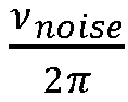
Claims (13)
- A quantum system (1) for stabilizing a cat qubit comprising:- a command circuit (5) including a microwave source (11) for delivering microwave radiation and a DC voltage source (13) for delivering DC voltage, and- a non-linear superconducting quantum circuit (3) including a non-linear element (7), said non-linear element (7) including at least one Josephson junction (17, 41, 43), a first resonant portion (27) having a first mode (a) with a first resonant frequency and a second resonant portion (29) having a second mode (b) with a second resonant frequency, said non-linear element (7) being coupled to the first resonant portion (27) and the second resonant portion (29),said quantum system (1) being arranged such that, when• the microwave source (11) delivers microwave radiation at a frequency substantially equal to the second resonant frequency to the second resonant portion (29) to drive the second mode (b), and• the DC voltage source (13) delivers DC voltage to bias the non-linear element (7), with the delivered DC voltage having a value inducing a microwave oscillation having a frequency substantially equal to the absolute value of the difference between twice the first resonant frequency and the second resonant frequency in the non-linear superconducting quantum circuit (3),the non-linear superconducting quantum circuit (3) stabilizes a two-dimensional manifold hosting said cat qubit.
- The quantum system (1) of claim 1, wherein the DC voltage source (13) is an ideal DC voltage source (13).
- The quantum system (1) of claim 1, comprising a resistive element (45) coupled to said DC voltage source (13), and wherein the command circuit (5) comprises an additional microwave source (15) arranged to deliver to the DC voltage source (13) microwave radiation at a frequency derived from the frequency of the microwave oscillation induced by the DC voltage source (13) to cause injection locking thereof.
- The quantum system (1) of claim 3, wherein said resistive element (45) is incorporated within the non-linear superconducting quantum circuit (3).
- The quantum system (1) of claim 3, wherein said resistive element (45) is incorporated within the command circuit (5).
- The quantum system (1) of one of claims 3 to 5, wherein the additional microwave source (15) is arranged to deliver microwave radiation at a frequency fL satisfying the condition

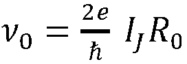
- The quantum system (1) of one of the preceding claims, wherein the non-linear element (7) includes only one Josephson junction (17), and wherein the DC voltage source (13) is arranged to deliver DC voltage having a value VDC verifying


- The quantum system (1) of one of claims 1 to 6, wherein the non-linear element (7) includes a plurality of Josephson junctions (17, 41, 43), and wherein the DC voltage source (13) is arranged to deliver DC voltage having a value VDC verifying


- The quantum system (1) of any one of the preceding claims, wherein the non-linear element (7) is galvanically coupled to the first resonant portion (27).
- The quantum system (1) of one of claims 1 to 8, wherein the non-linear element (7) is capacitively coupled to the first resonant portion (27).
- The quantum system (1) of one of the preceding claims, wherein the non-linear element (7) is galvanically coupled to the second resonant portion (29).
- The quantum system (1) of one of claims 1 to 10, wherein the non-linear element (7) is capacitively coupled to the second resonant portion (29).
- A method for stabilizing a cat qubit implemented by the quantum system (1) of one of the preceding claims and comprising the following operations:- delivering, by the microwave source (11), microwave radiation at a frequency substantially equal to the second resonant frequency to the second resonant portion (29) to drive the second mode (b), and- delivering, by the DC voltage source (13), DC voltage to bias the non-linear element (7), with the delivered DC voltage having a value inducing a microwave oscillation having a frequency substantially equal to the absolute value of the difference between twice the first resonant frequency and the second resonant frequency in the non-linear superconducting quantum circuit (3).
Priority Applications (2)
| Application Number | Priority Date | Filing Date | Title |
|---|---|---|---|
| EP23306839.4A EP4542455A1 (en) | 2023-10-19 | 2023-10-19 | A quantum system comprising a dc voltage source for stabilizing a cat qubit |
| PCT/EP2024/079392 WO2025083155A1 (en) | 2023-10-19 | 2024-10-17 | A quantum system comprising a dc voltage source for stabilizing a cat qubit |
Applications Claiming Priority (1)
| Application Number | Priority Date | Filing Date | Title |
|---|---|---|---|
| EP23306839.4A EP4542455A1 (en) | 2023-10-19 | 2023-10-19 | A quantum system comprising a dc voltage source for stabilizing a cat qubit |
Publications (1)
| Publication Number | Publication Date |
|---|---|
| EP4542455A1 true EP4542455A1 (en) | 2025-04-23 |
Family
ID=89222734
Family Applications (1)
| Application Number | Title | Priority Date | Filing Date |
|---|---|---|---|
| EP23306839.4A Pending EP4542455A1 (en) | 2023-10-19 | 2023-10-19 | A quantum system comprising a dc voltage source for stabilizing a cat qubit |
Country Status (2)
| Country | Link |
|---|---|
| EP (1) | EP4542455A1 (en) |
| WO (1) | WO2025083155A1 (en) |
-
2023
- 2023-10-19 EP EP23306839.4A patent/EP4542455A1/en active Pending
-
2024
- 2024-10-17 WO PCT/EP2024/079392 patent/WO2025083155A1/en active Pending
Non-Patent Citations (7)
| Title |
|---|
| A. MARQUET ET AL: "Autoparametric resonance extending the bit-flip time of a cat qubit up to 0.3 s", ARXIV.ORG, CORNELL UNIVERSITY LIBRARY, 201 OLIN LIBRARY CORNELL UNIVERSITY ITHACA, NY 14853, 13 July 2023 (2023-07-13), XP091562115, DOI: 10.48550/arXiv.2307.06761 * |
| A. PEUGEOT ET AL: "Generating two continuous entangled microwave beams using a dc-biased Josephson junction", ARXIV.ORG, CORNELL UNIVERSITY LIBRARY, 201 OLIN LIBRARY CORNELL UNIVERSITY ITHACA, NY 14853, 7 October 2020 (2020-10-07), XP081780691, DOI: 10.48550/arXiv.2010.03376 * |
| K. WOOD ET AL: "Josephson photonics with simultaneous resonances", ARXIV.ORG, CORNELL UNIVERSITY LIBRARY, 201 OLIN LIBRARY CORNELL UNIVERSITY ITHACA, NY 14853, 4 October 2021 (2021-10-04), XP091068411, DOI: 10.48550/arXiv.2106.15243 * |
| L. DANNER ET AL: "Injection locking and synchronization in Josephson photonics devices", ARXIV.ORG, CORNELL UNIVERSITY LIBRARY, 201 OLIN LIBRARY CORNELL UNIVERSITY ITHACA, NY 14853, 6 May 2021 (2021-05-06), XP081958580, DOI: 10.48550/arXiv.2105.02564 * |
| R. LESCANNE ET AL.: "Exponential suppression of bit flips in a qubit encoded in an oscillator", NATURE PHYSICS, 2020 |
| S.-L. MA ET AL: "Photon-pair blockade in a Josephson-photonics circuit with two nondegenerate microwave resonators", NEW JOURNAL OF PHYSICS, vol. 24, 053001, 3 May 2022 (2022-05-03), XP020422418, DOI: 10.1088/1367-2630/AC60DF * |
| U. R�GLADE ET AL: "Quantum control of a cat-qubit with bit-flip times exceeding ten seconds", ARXIV.ORG, CORNELL UNIVERSITY LIBRARY, 201 OLIN LIBRARY CORNELL UNIVERSITY ITHACA, NY 14853, 13 July 2023 (2023-07-13), XP091562280, DOI: 10.48550/arXiv.2307.06617 * |
Also Published As
| Publication number | Publication date |
|---|---|
| WO2025083155A1 (en) | 2025-04-24 |
Similar Documents
| Publication | Publication Date | Title |
|---|---|---|
| Conner et al. | Superconducting qubits in a flip-chip architecture | |
| US10719776B1 (en) | Quantum bit multi-state reset | |
| Xue et al. | Nonadiabatic holonomic quantum computation with dressed-state qubits | |
| US10572816B1 (en) | System and method for controlling superconducting qubits | |
| Appel et al. | Coherent spin-photon interface with waveguide induced cycling transitions | |
| US10127500B2 (en) | Quantum nondemolition microwave photon counter based on the cross-kerr nonlinearity of a josephson junction embedded in a superconducting circuit | |
| Chen et al. | Realization of a single-Cooper-pair Josephson laser | |
| Abdullaev et al. | Coherent atomic oscillations and resonances between coupled Bose-Einstein condensates with time-dependent trapping potential | |
| US20140368234A1 (en) | Multiple-qubit wave-activated controlled gate | |
| Pogorzalek et al. | Hysteretic flux response and nondegenerate gain of flux-driven Josephson parametric amplifiers | |
| Minev et al. | Planar multilayer circuit quantum electrodynamics | |
| WO2017115160A1 (en) | Multi-qubit tunable coupling architecture using fixed-frequency superconducting qubits | |
| Ito et al. | Four single-spin Rabi oscillations in a quadruple quantum dot | |
| US20180017603A1 (en) | Oscillation device, computing device, and measurement method | |
| JP7609533B2 (en) | Flux bias for pulse shaping of microwave signals. | |
| Xu et al. | Dynamic compensation for pump-induced frequency shift in Kerr-cat qubit initialization | |
| Bengtsson et al. | Quantum approximate optimization of the exact-cover problem on a superconducting quantum processor | |
| EP4720939A1 (en) | A quantum system for stabilizing a bosonic qubit | |
| Dassonneville et al. | Transmon-qubit readout using an in situ bifurcation amplification in the mesoscopic regime | |
| US20260012157A1 (en) | Superconducting quantum circuit for bosonic codes with galvanic coupling | |
| WO2025083155A1 (en) | A quantum system comprising a dc voltage source for stabilizing a cat qubit | |
| Széchenyi et al. | Coulomb-blockade and Pauli-blockade magnetometry | |
| US20260010814A1 (en) | Minimal superconducting quantum circuit for bosonic codes with galvanic coupling | |
| Mori et al. | High-power readout of a transmon qubit using a nonlinear coupling | |
| Van der Wiel et al. | Microwave spectroscopy of a double quantum dot in the low-and high-power regime |
Legal Events
| Date | Code | Title | Description |
|---|---|---|---|
| PUAI | Public reference made under article 153(3) epc to a published international application that has entered the european phase |
Free format text: ORIGINAL CODE: 0009012 |
|
| STAA | Information on the status of an ep patent application or granted ep patent |
Free format text: STATUS: THE APPLICATION HAS BEEN PUBLISHED |
|
| AK | Designated contracting states |
Kind code of ref document: A1 Designated state(s): AL AT BE BG CH CY CZ DE DK EE ES FI FR GB GR HR HU IE IS IT LI LT LU LV MC ME MK MT NL NO PL PT RO RS SE SI SK SM TR |
|
| STAA | Information on the status of an ep patent application or granted ep patent |
Free format text: STATUS: REQUEST FOR EXAMINATION WAS MADE |
|
| 17P | Request for examination filed |
Effective date: 20251016 |
|
| GRAP | Despatch of communication of intention to grant a patent |
Free format text: ORIGINAL CODE: EPIDOSNIGR1 |
|
| STAA | Information on the status of an ep patent application or granted ep patent |
Free format text: STATUS: GRANT OF PATENT IS INTENDED |
|
| INTG | Intention to grant announced |
Effective date: 20260127 |