EP4542338A1 - Storage element assembly and electronic device - Google Patents
Storage element assembly and electronic device Download PDFInfo
- Publication number
- EP4542338A1 EP4542338A1 EP24195587.1A EP24195587A EP4542338A1 EP 4542338 A1 EP4542338 A1 EP 4542338A1 EP 24195587 A EP24195587 A EP 24195587A EP 4542338 A1 EP4542338 A1 EP 4542338A1
- Authority
- EP
- European Patent Office
- Prior art keywords
- storage element
- element assembly
- electronic device
- connecting piece
- storage elements
- Prior art date
- Legal status (The legal status is an assumption and is not a legal conclusion. Google has not performed a legal analysis and makes no representation as to the accuracy of the status listed.)
- Pending
Links
Images



Classifications
-
- G—PHYSICS
- G06—COMPUTING OR CALCULATING; COUNTING
- G06F—ELECTRIC DIGITAL DATA PROCESSING
- G06F1/00—Details not covered by groups G06F3/00 - G06F13/00 and G06F21/00
- G06F1/16—Constructional details or arrangements
- G06F1/20—Cooling means
-
- H—ELECTRICITY
- H05—ELECTRIC TECHNIQUES NOT OTHERWISE PROVIDED FOR
- H05K—PRINTED CIRCUITS; CASINGS OR CONSTRUCTIONAL DETAILS OF ELECTRIC APPARATUS; MANUFACTURE OF ASSEMBLAGES OF ELECTRICAL COMPONENTS
- H05K1/00—Printed circuits
- H05K1/02—Details
- H05K1/0201—Thermal arrangements, e.g. for cooling, heating or preventing overheating
- H05K1/0203—Cooling of mounted components
- H05K1/0209—External configuration of printed circuit board adapted for heat dissipation, e.g. lay-out of conductors, coatings
-
- H—ELECTRICITY
- H10—SEMICONDUCTOR DEVICES; ELECTRIC SOLID-STATE DEVICES NOT OTHERWISE PROVIDED FOR
- H10W—GENERIC PACKAGES, INTERCONNECTIONS, CONNECTORS OR OTHER CONSTRUCTIONAL DETAILS OF DEVICES COVERED BY CLASS H10
- H10W40/00—Arrangements for thermal protection or thermal control
- H10W40/20—Arrangements for cooling
- H10W40/22—Arrangements for cooling characterised by their shape, e.g. having conical or cylindrical projections
-
- H—ELECTRICITY
- H05—ELECTRIC TECHNIQUES NOT OTHERWISE PROVIDED FOR
- H05K—PRINTED CIRCUITS; CASINGS OR CONSTRUCTIONAL DETAILS OF ELECTRIC APPARATUS; MANUFACTURE OF ASSEMBLAGES OF ELECTRICAL COMPONENTS
- H05K1/00—Printed circuits
- H05K1/02—Details
- H05K1/0201—Thermal arrangements, e.g. for cooling, heating or preventing overheating
- H05K1/0203—Cooling of mounted components
-
- H—ELECTRICITY
- H05—ELECTRIC TECHNIQUES NOT OTHERWISE PROVIDED FOR
- H05K—PRINTED CIRCUITS; CASINGS OR CONSTRUCTIONAL DETAILS OF ELECTRIC APPARATUS; MANUFACTURE OF ASSEMBLAGES OF ELECTRICAL COMPONENTS
- H05K1/00—Printed circuits
- H05K1/18—Printed circuits structurally associated with non-printed electric components
- H05K1/181—Printed circuits structurally associated with non-printed electric components associated with surface mounted components
-
- H—ELECTRICITY
- H05—ELECTRIC TECHNIQUES NOT OTHERWISE PROVIDED FOR
- H05K—PRINTED CIRCUITS; CASINGS OR CONSTRUCTIONAL DETAILS OF ELECTRIC APPARATUS; MANUFACTURE OF ASSEMBLAGES OF ELECTRICAL COMPONENTS
- H05K5/00—Casings, cabinets or drawers for electric apparatus
- H05K5/02—Details
- H05K5/0213—Venting apertures; Constructional details thereof
-
- H—ELECTRICITY
- H05—ELECTRIC TECHNIQUES NOT OTHERWISE PROVIDED FOR
- H05K—PRINTED CIRCUITS; CASINGS OR CONSTRUCTIONAL DETAILS OF ELECTRIC APPARATUS; MANUFACTURE OF ASSEMBLAGES OF ELECTRICAL COMPONENTS
- H05K7/00—Constructional details common to different types of electric apparatus
- H05K7/20—Modifications to facilitate cooling, ventilating, or heating
- H05K7/20009—Modifications to facilitate cooling, ventilating, or heating using a gaseous coolant in electronic enclosures
- H05K7/20136—Forced ventilation, e.g. by fans
- H05K7/20154—Heat dissipaters coupled to components
-
- H—ELECTRICITY
- H05—ELECTRIC TECHNIQUES NOT OTHERWISE PROVIDED FOR
- H05K—PRINTED CIRCUITS; CASINGS OR CONSTRUCTIONAL DETAILS OF ELECTRIC APPARATUS; MANUFACTURE OF ASSEMBLAGES OF ELECTRICAL COMPONENTS
- H05K2201/00—Indexing scheme relating to printed circuits covered by H05K1/00
- H05K2201/07—Electric details
- H05K2201/0707—Shielding
-
- H—ELECTRICITY
- H05—ELECTRIC TECHNIQUES NOT OTHERWISE PROVIDED FOR
- H05K—PRINTED CIRCUITS; CASINGS OR CONSTRUCTIONAL DETAILS OF ELECTRIC APPARATUS; MANUFACTURE OF ASSEMBLAGES OF ELECTRICAL COMPONENTS
- H05K2201/00—Indexing scheme relating to printed circuits covered by H05K1/00
- H05K2201/10—Details of components or other objects attached to or integrated in a printed circuit board
- H05K2201/10227—Other objects, e.g. metallic pieces
- H05K2201/10325—Sockets, i.e. female type connectors comprising metallic connector elements integrated in, or bonded to a common dielectric support
Definitions
- the present invention relates to a storage element, and more particularly to a storage element assembly installed in an electronic device, and the electronic device using the same.
- a common portable electronic device includes various electronic elements such as a battery, a processor, and a memory. Because the working efficiency of the electronic elements is affected by the temperature, how to dissipate heat is one of important design issues for portable electronic devices.
- the present invention provides a storage element assembly having a good heat dissipation effect.
- the present invention further provides an electronic device in which a storage element assembly has a good heat dissipation effect.
- an embodiment of the present invention provides a storage element assembly, including two storage elements and a connecting piece.
- Each storage element has a first side and a second side opposite to each other and a third side and a fourth side opposite to each other, the third side and the fourth side are connected between the first side and the second side, and the third sides of the storage elements are opposite to each other and spaced by a gap.
- the connecting piece has two wrapping portions and a bridging portion, each wrapping portion wraps the first side, the second side, and the fourth side of one of the storage elements, and the bridging portion is connected between the wrapping portions and covers the gap.
- the connecting piece comprises a metal layer and a wave-absorbing layer, the metal layer is superimposed on the wave-absorbing layer, and the wave-absorbing layer is located between the metal layer and the storage elements.
- the connecting piece further comprises an insulating layer, and the metal layer is located between the wave-absorbing layer and the insulating layer.
- each of the third sides is provided with an electrical connection portion.
- An embodiment of the present invention provides an electronic device, including a mainboard and the storage element assembly.
- the storage element assembly is arranged on the mainboard.
- the mainboard is provided with two connecting slots, each of the third sides is provided with an electrical connection portion, the electrical connection portions of the third sides are inserted into the connecting slots, respectively, and the bridging portion covers the connecting slots.
- the electronic device further includes a fan configured to generate an airflow, where the airflow passes through the connecting piece.
- the electronic device further includes a housing, where the housing includes an air inlet and an air outlet, the fan is arranged at the air outlet, the storage element assembly is located between the air inlet and the fan, and the airflow flows through a space between the connecting piece and the housing.
- the housing includes a bottom board and a side board, the air inlet is located on the bottom board, and the air outlet is located on the side board.
- the storage element assembly according to the present invention has good heat dissipation performance because the storage element assembly is wrapped by the wrapping portions of the connecting piece and the bridging portion capable of increasing a heat dissipation area is formed between the two wrapping portions.
- the electronic device according to the present invention includes the storage element assembly and thus has good heat dissipation performance.
- the two storage elements are both wrapped by the connecting piece, and the connecting slots for connecting the storage elements are also covered by the bridging portion, so signal interference caused by the storage elements can be reduced and thus interference noise can be reduced.
- orientation or position relation such as “above” and “below” are described according to the orientation or position relation shown in the drawings.
- the above terms are used for facilitating description of the present invention rather than limiting the present invention, i.e., indicating or implying that the mentioned elements have to have specific orientations and to be configured in the specific orientations.
- terms such as “first” and “second” involved in the description or claims are merely used for naming the elements or distinguishing different embodiments or ranges rather than limiting the upper limit or lower limit of the quantity of the elements.
- FIG. 1 is a schematic three-dimensional view of a storage element assembly according to an embodiment of the present invention.
- FIG. 2 is a schematic side view of the storage element assembly in the embodiment of FIG. 1 .
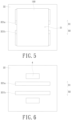
- FIG. 3 is a schematic diagram of a storage element in the embodiment of FIG. 1 .
- the elements in the drawings are all schematic only and not drawn to actual scale.
- a storage element assembly 100 in an embodiment includes two storage elements 1 and a connecting piece 2.
- Each storage element 1 has a first side 1a and a second side 1b opposite to each other and a third side 1c and a fourth side 1d opposite to each other.
- the third side 1c and the fourth side 1d are connected between the first side 1a and the second side 1b, and the third sides 1c of the two storage elements 1 are opposite to each other and spaced by a gap G.
- the connecting piece 2 has two wrapping portions 22 and a bridging portion 21. Each wrapping portion 22 wraps the first side 1a, the second side 1b, and the fourth side 1d of one of the storage elements 1, and the bridging portion 21 is connected between the wrapping portions 22 and covers the gap G.
- the storage element 1 is, for example, a memory installed in an electronic device 300 in FIG. 7 , but the type of the storage element 1 is not limited in the present invention.
- the electronic device 300 is, for example, a portable electronic device, such as a laptop or a tablet, but is not limited to this.
- Each storage element 1 has a body 11 and an electrical connection portion 12.
- the body 11 includes, for example, a substrate (not shown in figure) and a required electronic part (not shown in figure) as the memory.
- the body 11 has a fifth side 1e and a sixth side 1f opposite to each other along different directions.
- the fifth side 1e and the sixth side 1f are connected between the first side 1a and the second side 1b and are further connected between the third side 1c and the fourth side 1d.
- the fifth side 1e and the sixth side 1f of the storage element 1 are not covered by the connecting piece 2, but are not limited to this.
- the electrical connection portion 12 of the storage element 1 includes, for example, a plurality of connecting fingers (not shown in figure) suitable to be inserted and electrically connected into connecting slots (see 321a and 321b in FIG. 5 ) of the electronic device 300.
- the storage element assembly 100 is, for example, in a thin plate shape and has a first side S1 and a second side S2 opposite to each other, and the second side S2 is suitable to face a mainboard 32 of the electronic device 300 when the storage element assembly 100 is connected to the electronic device 300.
- the bridging portion 21 is located, for example, on the first side S1 of the storage element assembly 100.
- the wrapping portion 22 is, for example, a U-shaped groove, and openings of the two grooves formed by the two wrapping portions 22 are opposite to each other (see a position of the electrical connection portion 12 in FIG. 2 ).
- Each wrapping portion 22 includes a first portion 22a, a second portion 22b, and a turning portion 22c.
- the first portion 22a is adjacently connected to the bridging portion 21 and thus located on the first side 1a, while the second portion 22b is connected to the first portion 22a through the turning portion 22c and located on the second side S2 of the storage element assembly 100.
- FIG. 4 is a schematic structural diagram of a connecting piece in the embodiment of FIG. 1 .
- the connecting piece 2 is, for example, a flexible sheet and structurally includes an insulating layer 2a, a metal layer 2b, and a wave-absorbing layer 2c.
- the metal layer 2b is superimposed on the wave-absorbing layer 2c and located between the wave-absorbing layer 2c and the insulating layer 2a, for example, and during assembly, the wave-absorbing layer 2c is located between the metal layer 2b and the storage element 1 and thus may serve as the insulating layer.
- the specific arrangement of the metal layer 2b, the wave-absorbing layer 2c, and the insulating layer 2a is not limited to the above example, and relative positions thereof may be changed according to requirements.
- the insulating layer 2a may not be provided.
- the wave-absorbing layer 2c may be located between the metal layer 2b and the insulating layer 2a, and the connecting piece 2 is in contact with a surface of the storage element 1 via the insulating layer 2a.
- a number of the layers may also be changed according to requirements.
- the metal layer 2b is made of, but not limited to, aluminum foil, for example.
- the wave-absorbing layer 2c is made of, for example, an existing material that may be used to solve the problem of interference noise of electromagnetic waves, which may be selected according to requirements.
- the insulating layer 2a is made from, but not limited to, polyethylene terephthalate (PET), for example.
- FIG. 5 is a schematic diagram in which the storage element assembly according to the embodiment of FIG. 1 is installed on the mainboard.
- FIG. 6 is a schematic diagram in which the mainboard is not installed with the storage element assembly in the embodiment of FIG. 5 .
- FIG. 7 is a schematic diagram of a heat dissipation airflow of an electronic device in the embodiment of FIG. 1 .
- the electronic device 300 is, for example, a laptop and includes, for example, a mainboard 32, a housing 31, and a processor 33.
- the mainboard 32 is installed in the housing 31 and includes a connecting slot 321a, a connecting slot 321b, two thermally conductive pads 4, and a fan 313.
- the connecting slot 321a and the connecting slot 321b are parallel to each other, for example, and an opening direction D1 of the connecting slot 321a is opposite to an opening direction D2 of the connecting slot 321b.
- a distance between the connecting slot 321a and the connecting slot 321b corresponds to a length of the bridging portion 21, for example.
- the connecting piece 2 is suitable to press the two storage elements 1 against the connecting slot 321a and the connecting slot 321b through a tension provided by the bridging portion 21 and the first portions 22a located on two sides of the bridging portion 21, but is not limited to this.
- the two thermally conductive pads 4 are arranged on one side of the connecting slot 321a and one side of the connecting slot 321b, respectively, and one thermally conductive pad 4 is located in front of the opening direction D1 of the connecting slot 321a, while the other thermally conductive pad 4 is located in front of the opening direction D2 of the connecting slot 321b.
- the electrical connection portions 12 located on the third sides 1c of the storage elements 1 are inserted into the connecting slot 321a and the connecting slot 321b, respectively, and the bridging portion 21 covers the connecting slot 321a and the connecting slot 321b.
- the second portions 22b of the two wrapping portions 22 cover the two thermally conductive pads 4, respectively.
- the housing 31 has, for example, an air inlet 311 and an air outlet 312.
- the housing 31 further includes a bottom board 31a and a side board 31b.
- the bottom board 31a and the side board 31b are, for example, perpendicular to each other in this embodiment, but may form an angle in other embodiments.
- the air inlet 311 is located on the bottom board 31a
- the air outlet 312 is located on the side board 31b, but they are not limited thereto.
- the fan 313 is, but not limited to, a centrifugal fan 313, for example.
- the fan 313 is arranged in the housing 31 and located on one side of the air outlet 312, and is suitable to bring air from the air inlet 311 into an internal space of the housing 31 to generate an airflow W.
- the storage element assembly 100 is arranged between the air inlet 311 and the fan 313, allowing the airflow W to flow through a space between the connecting piece 2 and the housing 31.
- the airflow W flows through a surface of the first side S1 and can also flow through a surface (see FIG. 2 , the gap G) of the second side S2 where the bridging portion 21 is located.
- the processor 33 is arranged on the mainboard 32, for example, and is located in the housing 31 and on one side of the storage element assembly 100.
- Table 1 is an experimental table for comparing a temperature of the two storage elements 1 of the storage element assembly 100 in this embodiment with a temperature of two storage elements 1 of an existing storage element assembly (excluding the connecting piece 2). To distinguish the two storage elements 1, they are represented as a first storage element and a second storage element in Table 1.
- Table 1 Existing storage element assembly Storage element assembly 100 Ambient temperature (°C) 25 60 25 60 Temperature (°C) of first storage element 77.5 99.5 74.9 97.0 Temperature (°C) of second storage element 84.2 101.5 80.1 98.7 Temperature (°C) of bottom board 31a 50.1 49.4
- the two storage elements 1 of the storage element assembly 100 in this embodiment both have low temperatures, indicating that the storage element assembly 100 has good heat dissipation efficiency and the two storage elements 1 (the first storage element and the second storage element) in the storage element assembly 100 have a small temperature difference.
- FIG. 8 is a schematic diagram of comparing the embodiment of FIG. 1 with a control embodiment to measure interference noise.
- an instrument is arranged above the two connecting slots 321a and 321b (relative to the mainboard 32), where a line E1 in FIG. 8 represents noise measured in a control group installed with the existing storage element assembly, and a line E2 represents noise measured in an experimental group installed with the storage element assembly 100.
- a frequency band shown in a box A1 and a frequency band shown in a box A2 are a frequency band used by a global positioning system (GPS) and a frequency band used by a global navigation satellite system (GNSS), respectively.
- GPS global positioning system
- GNSS global navigation satellite system
- the noise measured by the experimental group is lower in all frequency ranges than the noise measured by the control group, indicating that the storage element assembly 100 in this embodiment has a function of reducing the interference noise.
- the storage element assembly according to the present invention has good heat dissipation performance because the storage element assembly is wrapped by the wrapping portions of the connecting piece and the bridging portion capable of increasing a heat dissipation area is formed between the two wrapping portions.
- the electronic device according to the present invention includes the storage element assembly and thus has good heat dissipation performance.
- the two storage elements are both wrapped by the connecting piece, and the connecting slots for connecting the storage elements are also covered by the bridging portion, so signal interference caused by the storage elements can be reduced and thus interference noise can be reduced.
Landscapes
- Engineering & Computer Science (AREA)
- Microelectronics & Electronic Packaging (AREA)
- Physics & Mathematics (AREA)
- Theoretical Computer Science (AREA)
- Thermal Sciences (AREA)
- Human Computer Interaction (AREA)
- General Engineering & Computer Science (AREA)
- General Physics & Mathematics (AREA)
- Shielding Devices Or Components To Electric Or Magnetic Fields (AREA)
Abstract
A storage element assembly includes two storage elements and a connecting piece. Each storage element has a first side and a second side opposite to each other and a third side and a fourth side opposite to each other, the third side and the fourth side are connected between the first side and the second side, and the third sides of the storage elements are opposite to each other and spaced by a gap. The connecting piece has two wrapping portions and a bridging portion, each wrapping portion wraps the first side, the second side, and the fourth side of one of the storage elements, and the bridging portion is connected between the wrapping portions and covers the gap. The present invention further provides an electronic device with the storage element assembly.
Description
- The present invention relates to a storage element, and more particularly to a storage element assembly installed in an electronic device, and the electronic device using the same.
- Portable electronic devices are important in the modern busy commercial society. A common portable electronic device includes various electronic elements such as a battery, a processor, and a memory. Because the working efficiency of the electronic elements is affected by the temperature, how to dissipate heat is one of important design issues for portable electronic devices.
- The present invention provides a storage element assembly having a good heat dissipation effect.
- The present invention further provides an electronic device in which a storage element assembly has a good heat dissipation effect.
- To achieve the above advantages, an embodiment of the present invention provides a storage element assembly, including two storage elements and a connecting piece. Each storage element has a first side and a second side opposite to each other and a third side and a fourth side opposite to each other, the third side and the fourth side are connected between the first side and the second side, and the third sides of the storage elements are opposite to each other and spaced by a gap. The connecting piece has two wrapping portions and a bridging portion, each wrapping portion wraps the first side, the second side, and the fourth side of one of the storage elements, and the bridging portion is connected between the wrapping portions and covers the gap.
- In an embodiment of the present invention, the connecting piece comprises a metal layer and a wave-absorbing layer, the metal layer is superimposed on the wave-absorbing layer, and the wave-absorbing layer is located between the metal layer and the storage elements.
- In an embodiment of the present invention, the connecting piece further comprises an insulating layer, and the metal layer is located between the wave-absorbing layer and the insulating layer.
- In an embodiment of the present invention, each of the third sides is provided with an electrical connection portion.
- An embodiment of the present invention provides an electronic device, including a mainboard and the storage element assembly. The storage element assembly is arranged on the mainboard.
- In an embodiment of the present invention, the mainboard is provided with two connecting slots, each of the third sides is provided with an electrical connection portion, the electrical connection portions of the third sides are inserted into the connecting slots, respectively, and the bridging portion covers the connecting slots.
- In an embodiment of the present invention, the electronic device further includes a fan configured to generate an airflow, where the airflow passes through the connecting piece.
- In an embodiment of the present invention, the electronic device further includes a housing, where the housing includes an air inlet and an air outlet, the fan is arranged at the air outlet, the storage element assembly is located between the air inlet and the fan, and the airflow flows through a space between the connecting piece and the housing.
- In an embodiment of the present invention, the housing includes a bottom board and a side board, the air inlet is located on the bottom board, and the air outlet is located on the side board.
- Based on the above description, the storage element assembly according to the present invention has good heat dissipation performance because the storage element assembly is wrapped by the wrapping portions of the connecting piece and the bridging portion capable of increasing a heat dissipation area is formed between the two wrapping portions. The electronic device according to the present invention includes the storage element assembly and thus has good heat dissipation performance. The two storage elements are both wrapped by the connecting piece, and the connecting slots for connecting the storage elements are also covered by the bridging portion, so signal interference caused by the storage elements can be reduced and thus interference noise can be reduced.
- Other objectives, features and advantages of the invention will be further understood from the further technological features disclosed by the embodiments of the invention wherein there are shown and described preferred embodiments of this invention, simply by way of illustration of modes best suited to carry out the invention.
-
-
FIG. 1 is a schematic three-dimensional view of a storage element assembly according to an embodiment of the present invention; -
FIG. 2 is a schematic side view of the storage element assembly in the embodiment ofFIG. 1 ; -
FIG. 3 is a schematic diagram of a storage element in the embodiment ofFIG. 1 ; -
FIG. 4 is a schematic structural diagram of a connecting piece in the embodiment ofFIG. 1 ; -
FIG. 5 is a schematic diagram in which the storage element assembly according to the embodiment ofFIG. 1 is installed on the mainboard; -
FIG. 6 is a schematic diagram in which the mainboard is not installed with the storage element assembly in the embodiment ofFIG. 5 ; -
FIG. 7 is a schematic diagram of a heat dissipation airflow of an electronic device in the embodiment ofFIG. 1 ; and -
FIG. 8 is a schematic diagram of comparing the embodiment ofFIG. 1 with a control embodiment to measure interference noise. - Terms used in the description of the embodiments of the present invention, for example, orientation or position relation such as "above" and "below" are described according to the orientation or position relation shown in the drawings. The above terms are used for facilitating description of the present invention rather than limiting the present invention, i.e., indicating or implying that the mentioned elements have to have specific orientations and to be configured in the specific orientations. In addition, terms such as "first" and "second" involved in the description or claims are merely used for naming the elements or distinguishing different embodiments or ranges rather than limiting the upper limit or lower limit of the quantity of the elements.
-
FIG. 1 is a schematic three-dimensional view of a storage element assembly according to an embodiment of the present invention.FIG. 2 is a schematic side view of the storage element assembly in the embodiment ofFIG. 1 .FIG. 3 is a schematic diagram of a storage element in the embodiment ofFIG. 1 . The elements in the drawings are all schematic only and not drawn to actual scale. As shown inFIG. 1 to FIG. 3 , astorage element assembly 100 in an embodiment includes twostorage elements 1 and a connectingpiece 2. Eachstorage element 1 has a first side 1a and asecond side 1b opposite to each other and athird side 1c and a fourth side 1d opposite to each other. Thethird side 1c and the fourth side 1d are connected between the first side 1a and thesecond side 1b, and thethird sides 1c of the twostorage elements 1 are opposite to each other and spaced by a gap G. The connectingpiece 2 has two wrappingportions 22 and abridging portion 21. Eachwrapping portion 22 wraps the first side 1a, thesecond side 1b, and the fourth side 1d of one of thestorage elements 1, and thebridging portion 21 is connected between thewrapping portions 22 and covers the gap G. - Specifically, as shown in
FIG. 3 , in this embodiment, thestorage element 1 is, for example, a memory installed in anelectronic device 300 inFIG. 7 , but the type of thestorage element 1 is not limited in the present invention. Theelectronic device 300 is, for example, a portable electronic device, such as a laptop or a tablet, but is not limited to this. Eachstorage element 1 has abody 11 and anelectrical connection portion 12. Thebody 11 includes, for example, a substrate (not shown in figure) and a required electronic part (not shown in figure) as the memory. In addition to the first side 1a, thesecond side 1b, thethird side 1c, and the fourth side 1d, thebody 11 has a fifth side 1e and a sixth side 1f opposite to each other along different directions. The fifth side 1e and the sixth side 1f are connected between the first side 1a and thesecond side 1b and are further connected between thethird side 1c and the fourth side 1d. In this embodiment, the fifth side 1e and the sixth side 1f of thestorage element 1 are not covered by the connectingpiece 2, but are not limited to this. Theelectrical connection portion 12 of thestorage element 1 includes, for example, a plurality of connecting fingers (not shown in figure) suitable to be inserted and electrically connected into connecting slots (see 321a and 321b inFIG. 5 ) of theelectronic device 300. - As shown in
FIG. 2 , thestorage element assembly 100 is, for example, in a thin plate shape and has a first side S1 and a second side S2 opposite to each other, and the second side S2 is suitable to face amainboard 32 of theelectronic device 300 when thestorage element assembly 100 is connected to theelectronic device 300. Thebridging portion 21 is located, for example, on the first side S1 of thestorage element assembly 100. The wrappingportion 22 is, for example, a U-shaped groove, and openings of the two grooves formed by the two wrappingportions 22 are opposite to each other (see a position of theelectrical connection portion 12 inFIG. 2 ). Eachwrapping portion 22 includes afirst portion 22a, asecond portion 22b, and aturning portion 22c. Thefirst portion 22a is adjacently connected to thebridging portion 21 and thus located on the first side 1a, while thesecond portion 22b is connected to thefirst portion 22a through theturning portion 22c and located on the second side S2 of thestorage element assembly 100. -
FIG. 4 is a schematic structural diagram of a connecting piece in the embodiment ofFIG. 1 . In this embodiment, the connectingpiece 2 is, for example, a flexible sheet and structurally includes aninsulating layer 2a, ametal layer 2b, and a wave-absorbing layer 2c. Themetal layer 2b is superimposed on the wave-absorbing layer 2c and located between the wave-absorbing layer 2c and theinsulating layer 2a, for example, and during assembly, the wave-absorbing layer 2c is located between themetal layer 2b and thestorage element 1 and thus may serve as the insulating layer. The specific arrangement of themetal layer 2b, the wave-absorbing layer 2c, and theinsulating layer 2a is not limited to the above example, and relative positions thereof may be changed according to requirements. For example, in embodiments not shown in figure, theinsulating layer 2a may not be provided. In other embodiments, the wave-absorbing layer 2c may be located between themetal layer 2b and the insulatinglayer 2a, and the connectingpiece 2 is in contact with a surface of thestorage element 1 via the insulatinglayer 2a. In addition, in some other embodiments, a number of the layers may also be changed according to requirements. Themetal layer 2b is made of, but not limited to, aluminum foil, for example. The wave-absorbing layer 2c is made of, for example, an existing material that may be used to solve the problem of interference noise of electromagnetic waves, which may be selected according to requirements. The insulatinglayer 2a is made from, but not limited to, polyethylene terephthalate (PET), for example. -
FIG. 5 is a schematic diagram in which the storage element assembly according to the embodiment ofFIG. 1 is installed on the mainboard.FIG. 6 is a schematic diagram in which the mainboard is not installed with the storage element assembly in the embodiment ofFIG. 5 .FIG. 7 is a schematic diagram of a heat dissipation airflow of an electronic device in the embodiment ofFIG. 1 . As shown inFIG. 5 to FIG. 7 , theelectronic device 300 is, for example, a laptop and includes, for example, amainboard 32, ahousing 31, and aprocessor 33. - The
mainboard 32 is installed in thehousing 31 and includes a connectingslot 321a, a connectingslot 321b, two thermallyconductive pads 4, and afan 313. The connectingslot 321a and the connectingslot 321b are parallel to each other, for example, and an opening direction D1 of the connectingslot 321a is opposite to an opening direction D2 of the connectingslot 321b. In this embodiment, a distance between the connectingslot 321a and the connectingslot 321b corresponds to a length of the bridgingportion 21, for example. In other words, in this embodiment, the connectingpiece 2 is suitable to press the twostorage elements 1 against the connectingslot 321a and the connectingslot 321b through a tension provided by the bridgingportion 21 and thefirst portions 22a located on two sides of the bridgingportion 21, but is not limited to this. - As shown in
FIG. 5 and FIG. 6 , the two thermallyconductive pads 4 are arranged on one side of the connectingslot 321a and one side of the connectingslot 321b, respectively, and one thermallyconductive pad 4 is located in front of the opening direction D1 of the connectingslot 321a, while the other thermallyconductive pad 4 is located in front of the opening direction D2 of the connectingslot 321b. There is no limitation on a material of the thermallyconductive pads 4, which may be selected according to requirements, and in other embodiments, a number of the thermallyconductive pads 4 may be increased. - As shown in
FIG. 2 ,FIG. 5, and FIG. 6 , when thestorage element assembly 100 is installed on themainboard 32, theelectrical connection portions 12 located on thethird sides 1c of thestorage elements 1 are inserted into the connectingslot 321a and the connectingslot 321b, respectively, and the bridgingportion 21 covers the connectingslot 321a and the connectingslot 321b. Thesecond portions 22b of the two wrappingportions 22 cover the two thermallyconductive pads 4, respectively. - As shown in
FIG. 7 , thehousing 31 has, for example, anair inlet 311 and anair outlet 312. Thehousing 31 further includes abottom board 31a and aside board 31b. Thebottom board 31a and theside board 31b are, for example, perpendicular to each other in this embodiment, but may form an angle in other embodiments. For example, theair inlet 311 is located on thebottom board 31a, and theair outlet 312 is located on theside board 31b, but they are not limited thereto. Thefan 313 is, but not limited to, acentrifugal fan 313, for example. Thefan 313 is arranged in thehousing 31 and located on one side of theair outlet 312, and is suitable to bring air from theair inlet 311 into an internal space of thehousing 31 to generate an airflow W. - As shown in
FIG. 7 , thestorage element assembly 100 is arranged between theair inlet 311 and thefan 313, allowing the airflow W to flow through a space between the connectingpiece 2 and thehousing 31. There is no limitation on an arrangement direction of the storage element assembly 100 (and the connectingslots FIG. 1 and FIG. 2 ). When passing through thestorage element assembly 100, the airflow W flows through a surface of the first side S1 and can also flow through a surface (seeFIG. 2 , the gap G) of the second side S2 where the bridgingportion 21 is located. Theprocessor 33 is arranged on themainboard 32, for example, and is located in thehousing 31 and on one side of thestorage element assembly 100. - To illustrate the advantages of the
storage element assembly 100, reference is made toFIG. 7 and Table 1 below. Table 1 is an experimental table for comparing a temperature of the twostorage elements 1 of thestorage element assembly 100 in this embodiment with a temperature of twostorage elements 1 of an existing storage element assembly (excluding the connecting piece 2). To distinguish the twostorage elements 1, they are represented as a first storage element and a second storage element in Table 1.Table 1 Existing storage element assembly Storage element assembly 100Ambient temperature (°C) 25 60 25 60 Temperature (°C) of first storage element 77.5 99.5 74.9 97.0 Temperature (°C) of second storage element 84.2 101.5 80.1 98.7 Temperature (°C) of bottom board 31a50.1 49.4 - It can be seen from
FIG. 7 that when theprocessor 33 as a heat source for theelectronic device 300 is close to thestorage element assembly 100, onestorage element 1 in thestorage element assembly 100 is closer to theprocessor 33 than theother storage element 1. Because theprocessor 33 is the heat source,different storage elements 1 will be affected by distances from theprocessor 33 and thus have a difference in temperature. Therefore, it can be seen in Table 1 that under the same ambient temperature, the two storage elements 1 (the first storage element and the second storage element) have different temperatures. - It can be seen from Table 1 that compared with the existing storage element assembly, the two
storage elements 1 of thestorage element assembly 100 in this embodiment both have low temperatures, indicating that thestorage element assembly 100 has good heat dissipation efficiency and the two storage elements 1 (the first storage element and the second storage element) in thestorage element assembly 100 have a small temperature difference. - Because noise of interference with wireless communication of the
electronic device 300 may be caused at positions where the connectingslot 321a and the connectingslot 321b are located, the interference noise caused at the positions is expected to be low in practice.FIG. 8 is a schematic diagram of comparing the embodiment ofFIG. 1 with a control embodiment to measure interference noise. In a measurement way, an instrument is arranged above the two connectingslots FIG. 8 represents noise measured in a control group installed with the existing storage element assembly, and a line E2 represents noise measured in an experimental group installed with thestorage element assembly 100. A frequency band shown in a box A1 and a frequency band shown in a box A2 are a frequency band used by a global positioning system (GPS) and a frequency band used by a global navigation satellite system (GNSS), respectively. - It can be seen from
FIG. 8 that compared with the noise measured by the control group, the noise measured by the experimental group is lower in all frequency ranges than the noise measured by the control group, indicating that thestorage element assembly 100 in this embodiment has a function of reducing the interference noise. - Based on the above description, the storage element assembly according to the present invention has good heat dissipation performance because the storage element assembly is wrapped by the wrapping portions of the connecting piece and the bridging portion capable of increasing a heat dissipation area is formed between the two wrapping portions. The electronic device according to the present invention includes the storage element assembly and thus has good heat dissipation performance. The two storage elements are both wrapped by the connecting piece, and the connecting slots for connecting the storage elements are also covered by the bridging portion, so signal interference caused by the storage elements can be reduced and thus interference noise can be reduced.
- While the invention has been described in terms of what is presently considered to be the most practical and preferred embodiments, it is to be understood that the invention needs not be limited to the disclosed embodiment. On the contrary, it is intended to cover various modifications and similar arrangements included within the spirit and scope of the appended claims which are to be accorded with the broadest interpretation so as to encompass all such modifications and similar structures.
Claims (10)
- A storage element assembly (100), comprising:two storage elements (1), wherein each of the two storage elements (1) has a first side (1a), a second side (1b), a third side (1c) and a fourth side (1d), the first side (1a) and the second side (1b) are opposite to each other, the third side (1c) and the fourth side (1d) are opposite to each other, the third side (1c) and the fourth side (1d) are connected between the first side (1a) and the second side (1b), and the third sides (1c) of the two storage elements (1) are opposite to each other and spaced by a gap (G); anda connecting piece (2), having two wrapping portions (22) and a bridging portion (21), wherein each of the two wrapping portions (22) wraps the first side (1a), the second side (1b), and the fourth side (1d) of one of the two storage elements (1), and the bridging portion (21) is connected between the two wrapping portions (22) and covers the gap (G).
- The storage element assembly (100) according to claim 1, wherein the connecting piece (2) comprises a metal layer (2b) and a wave-absorbing layer (2c), the metal layer (2b) is superimposed on the wave-absorbing layer (2c), and the wave-absorbing layer (2c) is located between the metal layer (2b) and the two storage elements (1).
- The storage element assembly (100) according to claim 2, wherein the connecting piece (2) further comprises an insulating layer (2a), and the metal layer (2b) is located between the wave-absorbing layer (2c) and the insulating layer (2a).
- The storage element assembly (100) according to any of claims 1 to 3, wherein each of the third sides (1c) is provided with an electrical connection portion (12).
- An electronic device (300), comprising:a mainboard (32); andthe storage element assembly (100) as claimed in any one of claims 1 to 4, arranged on the mainboard (32).
- The electronic device (300) according to claim 5, wherein the mainboard (32) is provided with two thermally conductive pads (4), and the two wrapping portions (22) are connected to the two thermally conductive pads (4), respectively.
- The electronic device (300) according to claim 5, wherein the mainboard (32) is provided with two connecting slots (321a, 321b), the electrical connection portions (12) of the third sides (1c) are inserted into the two connecting slots (321a, 321b), respectively, and the bridging portion (21) covers the two connecting slots (321a, 321b).
- The electronic device (300) according to any of claims 5 to 7, further comprising a fan (313) configured to generate an airflow (W), wherein the airflow (W) passes through the connecting piece (2).
- The electronic device (300) according to claim 8, further comprising a housing (31), wherein the housing (31) comprises an air inlet (311) and an air outlet (312), the fan (313) is arranged at the air outlet (312), the storage element assembly (100) is located between the air inlet (311) and the fan (313), and the airflow (W) flows through a space between the connecting piece (2) and the housing (31).
- The electronic device (300) according to claim 9, wherein the housing (31) comprises a bottom board (31a) and a side board (31b), the air inlet (311) is located on the bottom board (31a), and the air outlet (312) is located on the side board (31b).
Applications Claiming Priority (1)
| Application Number | Priority Date | Filing Date | Title |
|---|---|---|---|
| CN202311351627.7A CN119852255A (en) | 2023-10-18 | 2023-10-18 | Memory element group and electronic device |
Publications (1)
| Publication Number | Publication Date |
|---|---|
| EP4542338A1 true EP4542338A1 (en) | 2025-04-23 |
Family
ID=92503686
Family Applications (1)
| Application Number | Title | Priority Date | Filing Date |
|---|---|---|---|
| EP24195587.1A Pending EP4542338A1 (en) | 2023-10-18 | 2024-08-21 | Storage element assembly and electronic device |
Country Status (3)
| Country | Link |
|---|---|
| US (1) | US20250133650A1 (en) |
| EP (1) | EP4542338A1 (en) |
| CN (1) | CN119852255A (en) |
Citations (3)
| Publication number | Priority date | Publication date | Assignee | Title |
|---|---|---|---|---|
| US20060146497A1 (en) * | 2004-12-30 | 2006-07-06 | Intel Corporation | Heat exchanger for memory modules |
| GB2463538A (en) * | 2008-05-06 | 2010-03-24 | Ibm | Thermal linking of stacked memory modules to a main board or system enclosure |
| US20120050985A1 (en) * | 2010-08-31 | 2012-03-01 | Samsung Electronics Co., Ltd. | Electronic device having cooling structure |
-
2023
- 2023-10-18 CN CN202311351627.7A patent/CN119852255A/en active Pending
-
2024
- 2024-07-12 US US18/771,030 patent/US20250133650A1/en active Pending
- 2024-08-21 EP EP24195587.1A patent/EP4542338A1/en active Pending
Patent Citations (3)
| Publication number | Priority date | Publication date | Assignee | Title |
|---|---|---|---|---|
| US20060146497A1 (en) * | 2004-12-30 | 2006-07-06 | Intel Corporation | Heat exchanger for memory modules |
| GB2463538A (en) * | 2008-05-06 | 2010-03-24 | Ibm | Thermal linking of stacked memory modules to a main board or system enclosure |
| US20120050985A1 (en) * | 2010-08-31 | 2012-03-01 | Samsung Electronics Co., Ltd. | Electronic device having cooling structure |
Also Published As
| Publication number | Publication date |
|---|---|
| US20250133650A1 (en) | 2025-04-24 |
| CN119852255A (en) | 2025-04-18 |
Similar Documents
| Publication | Publication Date | Title |
|---|---|---|
| US11547018B2 (en) | Semiconductor storage device | |
| US11744046B2 (en) | Semiconductor storage device | |
| US7072181B2 (en) | Heat dissipating device and electronic apparatus including the same | |
| US20080080142A1 (en) | Electronic devices with enhanced heat spreading | |
| CN114243251A (en) | Vehicle body antenna module and method of cooling vehicle body antenna module | |
| CN216698367U (en) | Display module and display device | |
| CN107643806B (en) | Electronic equipment | |
| US12082332B2 (en) | Thermal management systems having signal transfer routing for use with electronic devices | |
| US20200409436A1 (en) | Electronic apparatus | |
| TWI768865B (en) | Antenna module and electronic device | |
| US9775265B2 (en) | Heatsink and circuit board with heatsink | |
| EP1178594B1 (en) | Electronic apparatus provided with an electronic circuit substrate | |
| CN115207611A (en) | Antenna modules and electronic devices | |
| EP4542338A1 (en) | Storage element assembly and electronic device | |
| US12505864B2 (en) | Semiconductor storage device | |
| US20040190249A1 (en) | Communication device | |
| US11013102B2 (en) | Printed circuit board and electronic device | |
| CN207070568U (en) | Cooling mechanism and active antenna system | |
| TWI862224B (en) | Storage element assembly and electronic device | |
| US12169644B2 (en) | Memory system | |
| JP2002334958A (en) | Heat-dissipating device | |
| US7239514B2 (en) | Heat transfer structure for electronic devices | |
| US20240072010A1 (en) | Package | |
| CN222869281U (en) | Circuit board assembly and electronic equipment | |
| US20240268074A1 (en) | Heat dissipation structure for heating element |
Legal Events
| Date | Code | Title | Description |
|---|---|---|---|
| PUAI | Public reference made under article 153(3) epc to a published international application that has entered the european phase |
Free format text: ORIGINAL CODE: 0009012 |
|
| STAA | Information on the status of an ep patent application or granted ep patent |
Free format text: STATUS: THE APPLICATION HAS BEEN PUBLISHED |
|
| AK | Designated contracting states |
Kind code of ref document: A1 Designated state(s): AL AT BE BG CH CY CZ DE DK EE ES FI FR GB GR HR HU IE IS IT LI LT LU LV MC ME MK MT NL NO PL PT RO RS SE SI SK SM TR |
|
| STAA | Information on the status of an ep patent application or granted ep patent |
Free format text: STATUS: REQUEST FOR EXAMINATION WAS MADE |
|
| 17P | Request for examination filed |
Effective date: 20250901 |