EP4541475A1 - Tap processing method for acm panel - Google Patents
Tap processing method for acm panel Download PDFInfo
- Publication number
- EP4541475A1 EP4541475A1 EP23204858.7A EP23204858A EP4541475A1 EP 4541475 A1 EP4541475 A1 EP 4541475A1 EP 23204858 A EP23204858 A EP 23204858A EP 4541475 A1 EP4541475 A1 EP 4541475A1
- Authority
- EP
- European Patent Office
- Prior art keywords
- burring
- burr
- skin
- processing method
- acm
- Prior art date
- Legal status (The legal status is an assumption and is not a legal conclusion. Google has not performed a legal analysis and makes no representation as to the accuracy of the status listed.)
- Withdrawn
Links
Images



Classifications
-
- B—PERFORMING OPERATIONS; TRANSPORTING
- B21—MECHANICAL METAL-WORKING WITHOUT ESSENTIALLY REMOVING MATERIAL; PUNCHING METAL
- B21D—WORKING OR PROCESSING OF SHEET METAL OR METAL TUBES, RODS OR PROFILES WITHOUT ESSENTIALLY REMOVING MATERIAL; PUNCHING METAL
- B21D31/00—Other methods for working sheet metal, metal tubes, metal profiles
- B21D31/02—Stabbing or piercing, e.g. for making sieves
-
- B—PERFORMING OPERATIONS; TRANSPORTING
- B21—MECHANICAL METAL-WORKING WITHOUT ESSENTIALLY REMOVING MATERIAL; PUNCHING METAL
- B21D—WORKING OR PROCESSING OF SHEET METAL OR METAL TUBES, RODS OR PROFILES WITHOUT ESSENTIALLY REMOVING MATERIAL; PUNCHING METAL
- B21D19/00—Flanging or other edge treatment, e.g. of tubes
- B21D19/08—Flanging or other edge treatment, e.g. of tubes by single or successive action of pressing tools, e.g. vice jaws
- B21D19/088—Flanging or other edge treatment, e.g. of tubes by single or successive action of pressing tools, e.g. vice jaws for flanging holes
-
- B—PERFORMING OPERATIONS; TRANSPORTING
- B23—MACHINE TOOLS; METAL-WORKING NOT OTHERWISE PROVIDED FOR
- B23G—THREAD CUTTING; WORKING OF SCREWS, BOLT HEADS, OR NUTS, IN CONJUNCTION THEREWITH
- B23G1/00—Thread cutting; Automatic machines specially designed therefor
- B23G1/16—Thread cutting; Automatic machines specially designed therefor in holes of workpieces by taps
-
- B—PERFORMING OPERATIONS; TRANSPORTING
- B23—MACHINE TOOLS; METAL-WORKING NOT OTHERWISE PROVIDED FOR
- B23P—METAL-WORKING NOT OTHERWISE PROVIDED FOR; COMBINED OPERATIONS; UNIVERSAL MACHINE TOOLS
- B23P15/00—Making specific metal objects by operations not covered by a single other subclass or a group in this subclass
-
- B—PERFORMING OPERATIONS; TRANSPORTING
- B23—MACHINE TOOLS; METAL-WORKING NOT OTHERWISE PROVIDED FOR
- B23P—METAL-WORKING NOT OTHERWISE PROVIDED FOR; COMBINED OPERATIONS; UNIVERSAL MACHINE TOOLS
- B23P17/00—Metal-working operations, not covered by a single other subclass or another group in this subclass
-
- B—PERFORMING OPERATIONS; TRANSPORTING
- B32—LAYERED PRODUCTS
- B32B—LAYERED PRODUCTS, i.e. PRODUCTS BUILT-UP OF STRATA OF FLAT OR NON-FLAT, e.g. CELLULAR OR HONEYCOMB, FORM
- B32B15/00—Layered products comprising a layer of metal
- B32B15/20—Layered products comprising a layer of metal comprising aluminium or copper
-
- B—PERFORMING OPERATIONS; TRANSPORTING
- B32—LAYERED PRODUCTS
- B32B—LAYERED PRODUCTS, i.e. PRODUCTS BUILT-UP OF STRATA OF FLAT OR NON-FLAT, e.g. CELLULAR OR HONEYCOMB, FORM
- B32B3/00—Layered products comprising a layer with external or internal discontinuities or unevennesses, or a layer of non-planar shape; Layered products comprising a layer having particular features of form
- B32B3/02—Layered products comprising a layer with external or internal discontinuities or unevennesses, or a layer of non-planar shape; Layered products comprising a layer having particular features of form characterised by features of form at particular places, e.g. in edge regions
- B32B3/06—Layered products comprising a layer with external or internal discontinuities or unevennesses, or a layer of non-planar shape; Layered products comprising a layer having particular features of form characterised by features of form at particular places, e.g. in edge regions for securing layers together; for attaching the product to another member, e.g. to a support, or to another product, e.g. groove/tongue, interlocking
-
- B—PERFORMING OPERATIONS; TRANSPORTING
- B21—MECHANICAL METAL-WORKING WITHOUT ESSENTIALLY REMOVING MATERIAL; PUNCHING METAL
- B21D—WORKING OR PROCESSING OF SHEET METAL OR METAL TUBES, RODS OR PROFILES WITHOUT ESSENTIALLY REMOVING MATERIAL; PUNCHING METAL
- B21D35/00—Combined processes according to or processes combined with methods covered by groups B21D1/00 - B21D31/00
- B21D35/002—Processes combined with methods covered by groups B21D1/00 - B21D31/00
- B21D35/005—Processes combined with methods covered by groups B21D1/00 - B21D31/00 characterized by the material of the blank or the workpiece
- B21D35/007—Layered blanks
-
- B—PERFORMING OPERATIONS; TRANSPORTING
- B21—MECHANICAL METAL-WORKING WITHOUT ESSENTIALLY REMOVING MATERIAL; PUNCHING METAL
- B21D—WORKING OR PROCESSING OF SHEET METAL OR METAL TUBES, RODS OR PROFILES WITHOUT ESSENTIALLY REMOVING MATERIAL; PUNCHING METAL
- B21D53/00—Making other particular articles
- B21D53/24—Making other particular articles nuts or like thread-engaging members
-
- B—PERFORMING OPERATIONS; TRANSPORTING
- B32—LAYERED PRODUCTS
- B32B—LAYERED PRODUCTS, i.e. PRODUCTS BUILT-UP OF STRATA OF FLAT OR NON-FLAT, e.g. CELLULAR OR HONEYCOMB, FORM
- B32B15/00—Layered products comprising a layer of metal
- B32B15/04—Layered products comprising a layer of metal comprising metal as the main or only constituent of a layer, which is next to another layer of the same or of a different material
- B32B15/06—Layered products comprising a layer of metal comprising metal as the main or only constituent of a layer, which is next to another layer of the same or of a different material of natural rubber or synthetic rubber
-
- H—ELECTRICITY
- H10—SEMICONDUCTOR DEVICES; ELECTRIC SOLID-STATE DEVICES NOT OTHERWISE PROVIDED FOR
- H10K—ORGANIC ELECTRIC SOLID-STATE DEVICES
- H10K59/00—Integrated devices, or assemblies of multiple devices, comprising at least one organic light-emitting element covered by group H10K50/00
- H10K59/80—Constructional details
- H10K59/87—Passivation; Containers; Encapsulations
- H10K59/871—Self-supporting sealing arrangements
-
- H—ELECTRICITY
- H10—SEMICONDUCTOR DEVICES; ELECTRIC SOLID-STATE DEVICES NOT OTHERWISE PROVIDED FOR
- H10K—ORGANIC ELECTRIC SOLID-STATE DEVICES
- H10K59/00—Integrated devices, or assemblies of multiple devices, comprising at least one organic light-emitting element covered by group H10K50/00
- H10K59/80—Constructional details
- H10K59/8794—Arrangements for heating and cooling
Definitions
- the present disclosure relates to a tap processing method for an aluminum composite material (ACM) panel, which is used to attach a system board to an ACM panel material back cover of a display device.
- ACM aluminum composite material
- OLEDs each include a hole injection electrode, an organic light emitting layer, and an electron injection electrode and emit light by energy generated when excitons generated by combining electrons and holes inside the organic light emitting layer fall from an excited state to a ground state.
- OLEDs include an OLED panel including organic light emitting layers therein and a back cover coupled to the OLED panel to support the OLED panel, and a system board is provided on a rear surface of the back cover.
- the organic light emitting layer of the OLED panel is degraded.
- the degraded organic light emitting layer is denatured and decomposed, thereby causing degradation of image quality such as afterimages due to differences in luminance between pixels and degradation of lifetime.
- the back cover needs to be made of a material having high rigidity and high thermal conductivity to stably support the OLED panel, and at the same time, facilitate discharge of the operating heat.
- an ACM panel is used as a material of the back cover.
- the ACM panel includes a metallic inner skin, a metallic outer skin, and a resin core layer between both skins, has significant structural strength and heat dissipation performance as compared to a thickness thereof, and thus is suitable as the material of the back cover.
- a system board 5 is mounted on a forming part of a back cover 8 and fastened to the back cover 8 using a screw coupling method.
- the ACM panel constituting the back cover 8 is very thin, a tap cannot be processed to have a depth enough to maintain strong screw fastening strength.
- the screw is fastened by adding a reinforcement plate to a screw fastening portion of the back cover 8 and forming a tap communicating with the back cover 8 and the reinforcement plate.
- the screw is fastened by providing the back cover 8 with a PEM nut.
- the manufacturing costs of a product increase due to an increase in the number of components as auxiliary parts such as the reinforcement plate or the PEM nut are used.
- the present disclosure is directed to providing a tap processing method for an ACM panel, which is capable of forming, when a system board is attached to a back cover, a screw thread that may maintain sufficient screw fastening strength without using a separate auxiliary part by using the characteristics of the ACM panel.
- a tap processing method for an ACM panel which forms a screw thread in the ACM panel including a metallic inner skin, a metallic outer skin, and a resin core layer interposed between both skins, includes an inner burring operation of burring the inner skin of the ACM panel so that an inner burr formed in the inner skin extends toward the outer skin while compressing the core layer, an outer burring operation of burring the outer skin of the ACM panel so that the outer burr formed in the outer skin extends toward the inner skin while compressing the core layer and the inner burr and the outer burr are also continuously connected to each other, and a tapping operation of forming a continuous screw thread in the inner burr and the outer burr continuously connected to each other.
- Burring work in the inner burring operation and the outer burring operation may be performed by a scrapless burring punch (SBP).
- SBP scrapless burring punch
- the tap processing method may further include a reference point setting operation of setting a burring reference point so that the inner burr formed in the inner burring operation and the outer burr formed in the outer burring operation are concentrically aligned before the outer burring operation.
- the reference point setting operation may be performed such that, in the inner burring operation, the outer skin is punched by the punching part at a tip of the SBP and thus a punching hole serving as the burring reference point is formed.
- burring processing is performed by the SBP through the punching hole.
- a tap processing method for an ACM panel according to the present disclosure is intended to form a screw thread in an ACM panel 10 including an inner skin 12, an outer skin 14, and a core layer 16 interposed between both skins 12 and 14.
- the present disclosure may be applied when a hook is fastened instead of a screw.
- the inner skin 12 and the outer skin 14 of the ACM panel 10 applied to the present disclosure may be made of a metallic material (aluminum or the like) that may form burrs through a burring process, which will be described below.
- the core layer 16 may be made of a resin material that may form a relative repulsive stress while compressed as burrs 121 and 141 are formed in the inner skin 12 and the outer skin 14.
- the tap processing method for the ACM panel according to the present disclosure includes the following operations.
- burring work in the inner burring operation and the outer burring operation is performed by a scrapless burring punch (SBP) 20, and the SBP 20 includes a punching part 201 constituting a tip and a burring part 202 whose diameter gradually increases from that of the punching part 201.
- SBP scrapless burring punch
- the SBP 20 is mainly used for a thin object such as a panel or a pipe and serves to form a burr as the object is punched by the punching part 201 and a punched peripheral part is bent by the burring part 202 in an entry direction.
- inner surfaces of the inner burr 121 and the outer burr 141 are subjected to tapping using a tool such as a tap drill 30 to form screw thread.
- the core layer 16 of the ACM panel 10 is compressed in a transverse direction, and thus the compressed core layer 16 applies relatively strong stress to the inner burr 121 and the outer burr 141.
- the present disclosure further includes a reference point setting operation of setting a burring reference point so that the inner burr 121 formed in the inner burring operation and the outer burr 141 formed in the outer burring operation may be concentrically aligned before the outer burring operation.
- the reference point setting operation may be performed such that, in the inner burring operation, the outer skin 14 is punched by the punching part 201 at the tip of the SBP 20 and thus a punching hole 14a serving as the burring reference point is formed (see FIG. 3A ).
- the stress of the ACM panel itself increases by burring processing without using a separate auxiliary part for increasing the fastening strength of the screw, and thus the fastening strength of the screw is stably maintained, which helps to improve the productivity of OLED display devices.
Landscapes
- Engineering & Computer Science (AREA)
- Mechanical Engineering (AREA)
- Devices For Indicating Variable Information By Combining Individual Elements (AREA)
Abstract
Description
- The present disclosure relates to a tap processing method for an aluminum composite material (ACM) panel, which is used to attach a system board to an ACM panel material back cover of a display device.
- Organic light emitting diodes (OLEDs) each include a hole injection electrode, an organic light emitting layer, and an electron injection electrode and emit light by energy generated when excitons generated by combining electrons and holes inside the organic light emitting layer fall from an excited state to a ground state.
- Based on this principle, OLEDs have self-luminous properties and do not require a separate light source unlike liquid crystal displays, and thus a thickness and weight thereof may be reduced.
- Further, since OLEDs exhibit high-quality properties such as low power consumption, high luminance, and a high response speed, an OLED is considered to be a next-generation display device for a portable electronic device.
- In general, OLEDs include an OLED panel including organic light emitting layers therein and a back cover coupled to the OLED panel to support the OLED panel, and a system board is provided on a rear surface of the back cover.
- Meanwhile, when an OLED is operating, high-temperature operating heat generated from the system board provided on the rear surface of the back cover is transferred to the OLED panel, and thus the organic light emitting layer of the OLED panel is degraded. In this case, the degraded organic light emitting layer is denatured and decomposed, thereby causing degradation of image quality such as afterimages due to differences in luminance between pixels and degradation of lifetime.
- Thus, the back cover needs to be made of a material having high rigidity and high thermal conductivity to stably support the OLED panel, and at the same time, facilitate discharge of the operating heat. In order to satisfy this condition, in recent years, an ACM panel is used as a material of the back cover.
- The ACM panel includes a metallic inner skin, a metallic outer skin, and a resin core layer between both skins, has significant structural strength and heat dissipation performance as compared to a thickness thereof, and thus is suitable as the material of the back cover.
- Meanwhile, as illustrated in
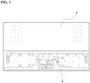
FIG. 1 , asystem board 5 is mounted on a forming part of aback cover 8 and fastened to theback cover 8 using a screw coupling method. In this case, since the ACM panel constituting theback cover 8 is very thin, a tap cannot be processed to have a depth enough to maintain strong screw fastening strength. - In the related art, in order to solve this problem, the screw is fastened by adding a reinforcement plate to a screw fastening portion of the
back cover 8 and forming a tap communicating with theback cover 8 and the reinforcement plate. Alternatively, the screw is fastened by providing theback cover 8 with a PEM nut. - However, according to the related art, the manufacturing costs of a product increase due to an increase in the number of components as auxiliary parts such as the reinforcement plate or the PEM nut are used.
- The present disclosure is directed to providing a tap processing method for an ACM panel, which is capable of forming, when a system board is attached to a back cover, a screw thread that may maintain sufficient screw fastening strength without using a separate auxiliary part by using the characteristics of the ACM panel.
- A tap processing method for an ACM panel, which forms a screw thread in the ACM panel including a metallic inner skin, a metallic outer skin, and a resin core layer interposed between both skins, includes an inner burring operation of burring the inner skin of the ACM panel so that an inner burr formed in the inner skin extends toward the outer skin while compressing the core layer, an outer burring operation of burring the outer skin of the ACM panel so that the outer burr formed in the outer skin extends toward the inner skin while compressing the core layer and the inner burr and the outer burr are also continuously connected to each other, and a tapping operation of forming a continuous screw thread in the inner burr and the outer burr continuously connected to each other.
- Burring work in the inner burring operation and the outer burring operation may be performed by a scrapless burring punch (SBP).
- The tap processing method may further include a reference point setting operation of setting a burring reference point so that the inner burr formed in the inner burring operation and the outer burr formed in the outer burring operation are concentrically aligned before the outer burring operation.
- The reference point setting operation may be performed such that, in the inner burring operation, the outer skin is punched by the punching part at a tip of the SBP and thus a punching hole serving as the burring reference point is formed.
- In the outer burring operation, burring processing is performed by the SBP through the punching hole.
- The above and other objects, features and advantages of the present disclosure will become more apparent to those of ordinary skill in the art by describing exemplary embodiments thereof in detail with reference to the accompanying drawings, in which:
-
FIG. 1 is a view illustrating a configuration in which a system board is attached to a back cover; -
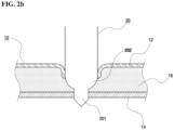
FIGS. 2A and2B are views sequentially illustrating an inner burring operation according to the present disclosure; -
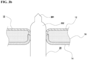
FIGS. 3A and3B are views sequentially illustrating an outer burring operation according to the present disclosure; -
FIG. 4 is a view illustrating a tapping operation according to the present disclosure; and -
FIG. 5 is a view illustrating a state in which a screw thread is formed in the ACM panel according to the present disclosure. - Hereinafter, specific details for implementing the present disclosure will be described in detail with reference to
FIGS. 2 to 5 . - A tap processing method for an ACM panel according to the present disclosure is intended to form a screw thread in an ACM
panel 10 including aninner skin 12, anouter skin 14, and acore layer 16 interposed between bothskins - Here, the
inner skin 12 and theouter skin 14 of the ACMpanel 10 applied to the present disclosure may be made of a metallic material (aluminum or the like) that may form burrs through a burring process, which will be described below. Thecore layer 16 may be made of a resin material that may form a relative repulsive stress while compressed as burrs 121 and 141 are formed in theinner skin 12 and theouter skin 14. - Further, the ACM
panel 10 applied to the present disclosure is used as a back cover of a display device and thus may be limited to one having a thickness (0.25t or less) suitable for maintaining structural rigidity while a sufficient heat dissipation effect is possible. - The tap processing method for the ACM panel according to the present disclosure includes the following operations.
- 1) An inner burring operation of burring the
inner skin 12 of the ACMpanel 10 so that the inner burr 121 formed in theinner skin 12 extends toward theouter skin 14 while compressing the core layer 16 (seeFIGS. 2A and2B ). - 2) an outer burring operation of burring the
outer skin 14 of the ACMpanel 10 so that the outer burr 141 formed in theouter skin 14 extends toward theinner skin 12 while compressing thecore layer 16 and the inner burr 121 and the outer burr 141 are also continuously connected (seeFIGS. 3A and3B ). - 3) A tapping operation of forming a continuous screw thread in the inner burr 121 and the outer burr 141 that are continuously connected (see
FIG. 4 ). - Here, burring work in the inner burring operation and the outer burring operation is performed by a scrapless burring punch (SBP) 20, and the
SBP 20 includes apunching part 201 constituting a tip and aburring part 202 whose diameter gradually increases from that of thepunching part 201. - The
SBP 20 is mainly used for a thin object such as a panel or a pipe and serves to form a burr as the object is punched by thepunching part 201 and a punched peripheral part is bent by theburring part 202 in an entry direction. - Further, in the tapping operation, inner surfaces of the inner burr 121 and the outer burr 141 are subjected to tapping using a tool such as a
tap drill 30 to form screw thread. - Thus, according to the present disclosure, as illustrated in
FIG. 5 , by combination of the inner burr 121 formed in the inner burring operation and the outer burr 141 formed in the outer burring operation, thecore layer 16 of the ACMpanel 10 is compressed in a transverse direction, and thus thecompressed core layer 16 applies relatively strong stress to the inner burr 121 and the outer burr 141. - Thus, the fastening strength of a screw fastened to the inner burr 121 and the outer burr 141 increases, and as a result, when the
system board 5 is attached to theback cover 8, an attachment state of thesystem board 5 is firmly maintained without a separate auxiliary part. - Further, the present disclosure further includes a reference point setting operation of setting a burring reference point so that the inner burr 121 formed in the inner burring operation and the outer burr 141 formed in the outer burring operation may be concentrically aligned before the outer burring operation.
- The reference point setting operation may be performed such that, in the inner burring operation, the
outer skin 14 is punched by thepunching part 201 at the tip of theSBP 20 and thus apunching hole 14a serving as the burring reference point is formed (seeFIG. 3A ). - Thus, when the outer burring is performed through the
punching hole 14a formed in theouter skin 14, since the outer burr 141 and the inner burr 121 are concentrically aligned and are accurately continuously connected to each other, separate work for the concentric alignment of the inner burr 121 and the outer burr 141 is not required. - According to the present disclosure, when a system board is attached to a back cover of an ACM panel material using a screw, the stress of the ACM panel itself increases by burring processing without using a separate auxiliary part for increasing the fastening strength of the screw, and thus the fastening strength of the screw is stably maintained, which helps to improve the productivity of OLED display devices.
Claims (5)
- A tap processing method for an aluminum composite material (ACM) panel, which forms a screw thread in the ACM panel including a metallic inner skin, a metallic outer skin, and a resin core layer interposed between both skins, the tap processing method comprising:an inner burring operation of burring the inner skin of the ACM panel so that an inner burr formed in the inner skin extends toward the outer skin while compressing the core layer;an outer burring operation of burring the outer skin of the ACM panel so that the outer burr formed in the outer skin extends toward the inner skin while compressing the core layer and the inner burr and the outer burr are also continuously connected to each other; anda tapping operation of forming a continuous screw thread in the inner burr and the outer burr continuously connected to each other.
- The tap processing method of claim 1, wherein burring work in the inner burring operation and the outer burring operation is performed by a scrapless burring punch (SBP) including a punching part at a tip thereof and a burring part whose diameter gradually increases from that of the punching part.
- The tap processing method of claim 2, further comprising a reference point setting operation of setting a burring reference point so that the inner burr formed in the inner burring operation and the outer burr formed in the outer burring operation are concentrically aligned before the outer burring operation.
- The tap processing method of claim 3, wherein the reference point setting operation is performed such that, in the inner burring operation, the outer skin is punched by the punching part at the tip of the SBP and thus a punching hole serving as the burring reference point is formed.
- The tap processing method of claim 4, wherein, in the outer burring operation, burring processing is performed by the SBP through the punching hole.
Priority Applications (1)
| Application Number | Priority Date | Filing Date | Title |
|---|---|---|---|
| EP23204858.7A EP4541475A1 (en) | 2023-10-20 | 2023-10-20 | Tap processing method for acm panel |
Applications Claiming Priority (1)
| Application Number | Priority Date | Filing Date | Title |
|---|---|---|---|
| EP23204858.7A EP4541475A1 (en) | 2023-10-20 | 2023-10-20 | Tap processing method for acm panel |
Publications (1)
| Publication Number | Publication Date |
|---|---|
| EP4541475A1 true EP4541475A1 (en) | 2025-04-23 |
Family
ID=88506733
Family Applications (1)
| Application Number | Title | Priority Date | Filing Date |
|---|---|---|---|
| EP23204858.7A Withdrawn EP4541475A1 (en) | 2023-10-20 | 2023-10-20 | Tap processing method for acm panel |
Country Status (1)
| Country | Link |
|---|---|
| EP (1) | EP4541475A1 (en) |
Citations (5)
| Publication number | Priority date | Publication date | Assignee | Title |
|---|---|---|---|---|
| EP0633132A1 (en) * | 1993-06-26 | 1995-01-11 | VAW Aluminium AG | Sandwich panel with reinforced connecting holes and method for making it |
| JP2012020330A (en) * | 2010-07-16 | 2012-02-02 | Muramoto Kosakusho:Kk | Burring working method and burring working implement |
| EP2822759A1 (en) * | 2012-03-07 | 2015-01-14 | ThyssenKrupp Steel Europe AG | Lightweight plate, and construction comprising a lightweight plate |
| JP2020029876A (en) * | 2018-08-21 | 2020-02-27 | プレス工業株式会社 | Burring fastening method, burring fastening structure and burring punch |
| KR102160746B1 (en) * | 2019-06-28 | 2020-09-28 | 주식회사 오성디스플레이 | Tap processing method in ACM panel |
-
2023
- 2023-10-20 EP EP23204858.7A patent/EP4541475A1/en not_active Withdrawn
Patent Citations (5)
| Publication number | Priority date | Publication date | Assignee | Title |
|---|---|---|---|---|
| EP0633132A1 (en) * | 1993-06-26 | 1995-01-11 | VAW Aluminium AG | Sandwich panel with reinforced connecting holes and method for making it |
| JP2012020330A (en) * | 2010-07-16 | 2012-02-02 | Muramoto Kosakusho:Kk | Burring working method and burring working implement |
| EP2822759A1 (en) * | 2012-03-07 | 2015-01-14 | ThyssenKrupp Steel Europe AG | Lightweight plate, and construction comprising a lightweight plate |
| JP2020029876A (en) * | 2018-08-21 | 2020-02-27 | プレス工業株式会社 | Burring fastening method, burring fastening structure and burring punch |
| KR102160746B1 (en) * | 2019-06-28 | 2020-09-28 | 주식회사 오성디스플레이 | Tap processing method in ACM panel |
Similar Documents
| Publication | Publication Date | Title |
|---|---|---|
| JP6840783B2 (en) | Semiconductor device | |
| KR102160746B1 (en) | Tap processing method in ACM panel | |
| KR101418706B1 (en) | Chassis and method for producing chassis | |
| KR20210001926A (en) | OLED display device and the method for manufacturing method for the back cover of which | |
| WO2006010355A3 (en) | Top-emitting, electroluminescent component having at least one organic layer | |
| EP1748505A3 (en) | Organic electroluminescence device and method for fabricating the same | |
| EP4541475A1 (en) | Tap processing method for acm panel | |
| US20250135565A1 (en) | Tap processing method for acm panel | |
| JP2025165177A (en) | ACM panel tapping method | |
| EP4550997A3 (en) | An organic electronic device comprising an anode layer, a cathode layer, at least one emission layer (eml) and at least one hole injection layer (hil) | |
| US6770812B2 (en) | Metal housing with auxiliary parts glued to housing base | |
| US11355732B2 (en) | Display device and manufacturing method thereof | |
| KR102300952B1 (en) | Structure for fixing pem nut | |
| KR20210120324A (en) | OLED display device | |
| KR102232684B1 (en) | Manufacturing method for pem nut and the press unit for that | |
| JP7592802B2 (en) | Electrode connecting element, light emitting device including the same, and method for manufacturing the light emitting device | |
| KR102019995B1 (en) | Oled panel housing structure | |
| JP2017201600A (en) | Manufacturing method of organic EL panel | |
| CN100559628C (en) | Electroluminescence device | |
| CN219930223U (en) | Sputtering target structure | |
| KR20200078238A (en) | Oled panel housing structre | |
| KR100711876B1 (en) | Light-emitting display device and manufacturing method | |
| CN109676010A (en) | A kind of processing method of carbon fibre composite plate connecting hole | |
| KR20100113831A (en) | Oled and method for fabricating the same | |
| CN114199078A (en) | Preparation method and device of boron carbide composite ceramic process |
Legal Events
| Date | Code | Title | Description |
|---|---|---|---|
| PUAI | Public reference made under article 153(3) epc to a published international application that has entered the european phase |
Free format text: ORIGINAL CODE: 0009012 |
|
| STAA | Information on the status of an ep patent application or granted ep patent |
Free format text: STATUS: THE APPLICATION HAS BEEN PUBLISHED |
|
| AK | Designated contracting states |
Kind code of ref document: A1 Designated state(s): AL AT BE BG CH CY CZ DE DK EE ES FI FR GB GR HR HU IE IS IT LI LT LU LV MC ME MK MT NL NO PL PT RO RS SE SI SK SM TR |
|
| STAA | Information on the status of an ep patent application or granted ep patent |
Free format text: STATUS: REQUEST FOR EXAMINATION WAS MADE |
|
| STAA | Information on the status of an ep patent application or granted ep patent |
Free format text: STATUS: THE APPLICATION HAS BEEN WITHDRAWN |
|
| 17P | Request for examination filed |
Effective date: 20250922 |
|
| 18W | Application withdrawn |
Effective date: 20251015 |