EP4539270A1 - Light-emitting device - Google Patents
Light-emitting device Download PDFInfo
- Publication number
- EP4539270A1 EP4539270A1 EP23819766.9A EP23819766A EP4539270A1 EP 4539270 A1 EP4539270 A1 EP 4539270A1 EP 23819766 A EP23819766 A EP 23819766A EP 4539270 A1 EP4539270 A1 EP 4539270A1
- Authority
- EP
- European Patent Office
- Prior art keywords
- power supply
- light
- capacitor
- emitting device
- signal
- Prior art date
- Legal status (The legal status is an assumption and is not a legal conclusion. Google has not performed a legal analysis and makes no representation as to the accuracy of the status listed.)
- Pending
Links
Images





Classifications
-
- G—PHYSICS
- G01—MEASURING; TESTING
- G01S—RADIO DIRECTION-FINDING; RADIO NAVIGATION; DETERMINING DISTANCE OR VELOCITY BY USE OF RADIO WAVES; LOCATING OR PRESENCE-DETECTING BY USE OF THE REFLECTION OR RERADIATION OF RADIO WAVES; ANALOGOUS ARRANGEMENTS USING OTHER WAVES
- G01S7/00—Details of systems according to groups G01S13/00, G01S15/00, G01S17/00
- G01S7/48—Details of systems according to groups G01S13/00, G01S15/00, G01S17/00 of systems according to group G01S17/00
- G01S7/483—Details of pulse systems
- G01S7/484—Transmitters
-
- H—ELECTRICITY
- H05—ELECTRIC TECHNIQUES NOT OTHERWISE PROVIDED FOR
- H05B—ELECTRIC HEATING; ELECTRIC LIGHT SOURCES NOT OTHERWISE PROVIDED FOR; CIRCUIT ARRANGEMENTS FOR ELECTRIC LIGHT SOURCES, IN GENERAL
- H05B45/00—Circuit arrangements for operating light-emitting diodes [LED]
- H05B45/30—Driver circuits
- H05B45/37—Converter circuits
- H05B45/3725—Switched mode power supply [SMPS]
-
- G—PHYSICS
- G01—MEASURING; TESTING
- G01S—RADIO DIRECTION-FINDING; RADIO NAVIGATION; DETERMINING DISTANCE OR VELOCITY BY USE OF RADIO WAVES; LOCATING OR PRESENCE-DETECTING BY USE OF THE REFLECTION OR RERADIATION OF RADIO WAVES; ANALOGOUS ARRANGEMENTS USING OTHER WAVES
- G01S17/00—Systems using the reflection or reradiation of electromagnetic waves other than radio waves, e.g. lidar systems
- G01S17/88—Lidar systems specially adapted for specific applications
- G01S17/93—Lidar systems specially adapted for specific applications for anti-collision purposes
- G01S17/931—Lidar systems specially adapted for specific applications for anti-collision purposes of land vehicles
-
- G—PHYSICS
- G01—MEASURING; TESTING
- G01S—RADIO DIRECTION-FINDING; RADIO NAVIGATION; DETERMINING DISTANCE OR VELOCITY BY USE OF RADIO WAVES; LOCATING OR PRESENCE-DETECTING BY USE OF THE REFLECTION OR RERADIATION OF RADIO WAVES; ANALOGOUS ARRANGEMENTS USING OTHER WAVES
- G01S7/00—Details of systems according to groups G01S13/00, G01S15/00, G01S17/00
- G01S7/48—Details of systems according to groups G01S13/00, G01S15/00, G01S17/00 of systems according to group G01S17/00
- G01S7/481—Constructional features, e.g. arrangements of optical elements
- G01S7/4814—Constructional features, e.g. arrangements of optical elements of transmitters alone
- G01S7/4815—Constructional features, e.g. arrangements of optical elements of transmitters alone using multiple transmitters
-
- H—ELECTRICITY
- H01—ELECTRIC ELEMENTS
- H01S—DEVICES USING THE PROCESS OF LIGHT AMPLIFICATION BY STIMULATED EMISSION OF RADIATION [LASER] TO AMPLIFY OR GENERATE LIGHT; DEVICES USING STIMULATED EMISSION OF ELECTROMAGNETIC RADIATION IN WAVE RANGES OTHER THAN OPTICAL
- H01S5/00—Semiconductor lasers
- H01S5/04—Processes or apparatus for excitation, e.g. pumping, e.g. by electron beams
- H01S5/042—Electrical excitation ; Circuits therefor
- H01S5/0428—Electrical excitation ; Circuits therefor for applying pulses to the laser
-
- H—ELECTRICITY
- H01—ELECTRIC ELEMENTS
- H01S—DEVICES USING THE PROCESS OF LIGHT AMPLIFICATION BY STIMULATED EMISSION OF RADIATION [LASER] TO AMPLIFY OR GENERATE LIGHT; DEVICES USING STIMULATED EMISSION OF ELECTROMAGNETIC RADIATION IN WAVE RANGES OTHER THAN OPTICAL
- H01S5/00—Semiconductor lasers
- H01S5/06—Arrangements for controlling the laser output parameters, e.g. by operating on the active medium
- H01S5/062—Arrangements for controlling the laser output parameters, e.g. by operating on the active medium by varying the potential of the electrodes
- H01S5/06209—Arrangements for controlling the laser output parameters, e.g. by operating on the active medium by varying the potential of the electrodes in single-section lasers
- H01S5/06216—Pulse modulation or generation
-
- H—ELECTRICITY
- H01—ELECTRIC ELEMENTS
- H01S—DEVICES USING THE PROCESS OF LIGHT AMPLIFICATION BY STIMULATED EMISSION OF RADIATION [LASER] TO AMPLIFY OR GENERATE LIGHT; DEVICES USING STIMULATED EMISSION OF ELECTROMAGNETIC RADIATION IN WAVE RANGES OTHER THAN OPTICAL
- H01S5/00—Semiconductor lasers
- H01S5/40—Arrangement of two or more semiconductor lasers, not provided for in groups H01S5/02 - H01S5/30
- H01S5/42—Arrays of surface emitting lasers
- H01S5/423—Arrays of surface emitting lasers having a vertical cavity
-
- H—ELECTRICITY
- H05—ELECTRIC TECHNIQUES NOT OTHERWISE PROVIDED FOR
- H05B—ELECTRIC HEATING; ELECTRIC LIGHT SOURCES NOT OTHERWISE PROVIDED FOR; CIRCUIT ARRANGEMENTS FOR ELECTRIC LIGHT SOURCES, IN GENERAL
- H05B45/00—Circuit arrangements for operating light-emitting diodes [LED]
- H05B45/10—Controlling the intensity of the light
Definitions
- a measurement device that measures a distance to an object on the basis of light emitted from a light emitting element such as a laser diode is generally provided with a drive circuit that drives the light emitting element (e.g., Patent Literature 1).
- Patent Literature 1 JP-A-2021-28924
- Patent Literature 1 The drive circuit disclosed in Patent Literature 1 is provided with a level shift circuit, and therefore, the configuration of the drive circuit is generally complicated.
- the present invention has been made in view of the above-described conventional problems, and an object of the present invention is to provide a light-emitting device capable of turning on a plurality of light sources with a simple configuration.
- One aspect of the present invention is a light-emitting device including n (n ⁇ 2) light sources, n power supply circuits each provided for the n light sources, and a switch provided between a ground-side node of each of the n light sources and a ground, each power supply circuit generates a power supply voltage for a corresponding one of the n light sources on the basis of a first signal, and stops generating the power supply voltage on the basis of a second signal, and the switch is turned on on the basis of a light-on instruction and is turned off on the basis of a light-off instruction when the power supply voltage for the one light source is generated.
- a measurement device 10 is a device that has the function of a so-called light detection and ranging or laser imaging detection and ranging (LiDAR) and measures a distance to an object 11. Specifically, the measurement device 10 emits measurement light and measures the distance to the object 11 on the basis of a time of flight (TOF) method for detecting light reflected by the surface of the object 11. Further, the measurement device 10 is installed, for example, in a vehicle (not shown), and includes a light-emitting device 20, a light receiving device 21, and a control device 22.
- TOF time of flight
- the object 11 is, for example, a vehicle different from the vehicle on which the measurement device 10 is installed, a person, or a structure such as a street lamp or a building.
- the light-emitting device 20 emits the measurement light to the object 11 under the control of the control device 22 (described later). Note that details of the light-emitting device 20 will be described later.
- the light receiving device 21 receives the reflected light from the object 11, and outputs information (e.g., timing or level) regarding the reflected light to the control device 22.
- information e.g., timing or level
- the control device 22 is a device that integrally controls the measurement device 10. Specifically, the control device 22 controls emission of the measurement light from the light-emitting device 20, and measures the distance to the object 11 by the time of flight (TOF) method on the basis of the output from the light receiving device 21. Note that although not shown in the figure, the control device 22 includes, for example, a storage device and an arithmetic device that executes a program stored in the storage device.
- Fig. 2 is a diagram showing one example of the configuration of a general light-emitting device 20a.
- the light-emitting device 20a includes light sources D0 to D9, a capacitor 40, power supply circuits 50 to 59, and a control circuit 60. Note that in Fig. 2 , for the sake of convenience, part of the configuration (light sources D2 to D8, power supply circuits 52 to 58) of the light-emitting device 20a is omitted.
- the cathodes of the laser diodes 100 to 115 are common, and the anodes are also common.
- the light emitted from each of the laser diodes 100 to 115 is the measurement light from one light source D0.
- the light source D0 includes the 16 laser diodes 100 to 115 here, but may include another number (for example, 8 or 32) of laser diodes.
- the optical member 120 is, for example, a light shaping diffuser (LSD), and is a member that diffuses (i.e., adjusts) the light emitted from each of the laser diodes 100 to 115 such that desired light distribution of the light from the light source D0 is obtained.
- LSD light shaping diffuser
- the LSD is used as the optical member 120 here, but any member may be used as long as the light distribution of the light from the light source D0 can be in a desired pattern.
- the capacitor 40 is an element that stabilizes a predetermined power supply voltage Vdd1 (e.g., several tens of V) supplied to the power supply circuits 50 to 59.
- the predetermined power supply voltage Vdd1 is applied to the capacitor 40.
- the power supply circuit 50 is a circuit that generates a power supply voltage V0 for turning on the light source D0 on the basis of the power supply voltage Vdd1 and a signal S0 from the control circuit 60. Specifically, the power supply circuit 50 generates the power supply voltage V0 when a high-level (hereinafter, "H-level”) signal S0 is input from the control circuit 60 to turn on the light source D0. On the other hand, the power supply circuit 50 stops generating the power supply voltage V0 when a low-level (hereinafter, "L-level”) signal S0 is input from the control circuit 60 to turn off the light source D0.
- H-level high-level
- L-level low-level
- the power supply circuit 50 includes a diode 200, a capacitor 201, a buffer 210, a transformer 211, an integrated circuit (IC) 212, and a resistor 213.
- the diode 200 is an element that generates a power supply voltage for operating the IC 212 (described later) together with the capacitor 201.
- a power supply voltage Vdd2 (e.g., 5 V) is applied to the anode of the diode 200, and the cathode of the diode 200 is connected to the capacitor 201.
- the buffer 210 outputs a signal Sa0 having the same logic level as that of the signal S0 to the transformer 211. Specifically, the buffer 210 outputs the H-level signal Sa0 on the basis of the H-level signal S0, and outputs the L-level signal Sa0 on the basis of the L-level signal S0.
- the signal S0 is a signal for controlling ON/OFF of a driving transistor 231 (described later) of the IC 212
- the L-level of the signal S0 is, for example, 0 V
- the H-level is, for example, 3 V.
- the transformer 211 is an isolated transformer that converts and outputs a DC level while maintaining the amplitude of an input signal, and includes a primary coil 220 and a secondary coil 221 electromagnetically coupled to the primary coil 220.
- the transformer 211 functions as a so-called level shift circuit.
- the transformer 211 converts the signal Sa0 of which the logic level changes with reference to a ground voltage (0 V) into a signal Sb0 changing with reference to the power supply voltage V0. That is, the transformer 211 causes the secondary coil 221 to generate the H-level signal Sb0 when the signal Sa0 is at the H-level, and causes the secondary coil 221 to generate the L-level signal Sb0 when the signal Sa0 is at the L-level.
- the transformer 211 is used as the so-called level shift circuit, but the present invention is not limited thereto and other configurations (e.g., circuit including a photocoupler) may be used.
- the IC 212 generates the power supply voltage V0 to the light source D0 when the signal Sb0 from the secondary coil 221 is at the H-level, and stops generating the power supply voltage V0 when the signal Sb0 is at the L-level.
- the IC 212 includes a buffer 230 and the driving transistor 231.
- the buffer 230 outputs the L-level signal to the driving transistor 231. As a result, the driving transistor 231 is turned off.
- the driving transistor 231 when the driving transistor 231 is turned on, the power supply voltage V0 of a line L0 on the anode side of the light source D0 increases to almost the power supply voltage Vdd1. Since the high-level power supply voltage V0 is applied to the line L0 on the anode side of the light source D0, the light source D0 is turned on (emits the measurement light).
- the resistor 213 is an element for limiting the current flowing through the light source D0.
- the driving transistor 231 When the driving transistor 231 is turned on, the voltage of the line L0 to which the source electrode of the driving transistor 231 is connected increases to almost the power supply voltage Vdd1 (e.g., several tens of V).
- Vdd1 e.g., several tens of V.
- the power supply circuit 50 stops generating the power supply voltage V0. As a result, the supply of the power supply voltage V0 to the light source D0 is also stopped, and therefore, the light source D0 is turned off.
- control circuit 60 sets the level of one signal corresponding to the light source to be turned on among the signals S0 to S9 to the H-level, and sets the levels of the other nine signals to the L-level. By outputting such signals S0 to S9, the light sources D0 to D9 are sequentially turned on.
- each of the power supply circuits 50 to 59 of the light-emitting device 20a of Fig. 2 includes many components such as the transformer 211 and the IC 212. For this reason, in general, a mounting space occupied by the power supply circuits 50 to 59 in the light-emitting device 20a is wide.
- the light-emitting device 20b shown in Fig. 4 is a device that turns on the light sources D0 to D9 on the basis of the light-on start instruction from the control device 22, and includes the light sources D0 to D9, the capacitor 40, an IC 41, power supply circuits 70 to 79, and a control circuit 80.
- the components denoted by the same reference numerals in Fig. 4 and Fig. 2 are the same as each other.
- the IC 41, the power supply circuits 70 to 79, and the control circuit 80 will be mainly described. Note that in Fig. 4 , for the sake of convenience, part of the configuration (light sources D2 to D8, power supply circuits 72 to 78) of the light-emitting device 20b is omitted.
- the IC 41 is a circuit similar to the IC 212 of Fig. 2 , and includes a buffer 300 and a driving transistor 301.
- the buffer 300 outputs a signal having the same logic level as that of the input signal to the driving transistor 301.
- a signal S20 from the control circuit 80 (described later) is input to the buffer 300.
- the buffer 300 turns on the driving transistor 301 on the basis of the H-level signal S20, and turns off the driving transistor 301 on the basis of the L-level signal S20.
- the H-level signal S20 corresponds to a "light-on instruction” for turning on the light source
- the L-level signal S20 corresponds to a "light-off instruction” for turning off the light source.
- the drain electrode is connected to the ground-side nodes of the light sources D0 to D9, and the source electrode is grounded.
- the driving transistor 301 when the driving transistor 301 is turned on, a current flows through the light source to which the power supply voltage is applied among the light sources D0 to D9, and such a light source is turned on.
- the driving transistor 301 when the driving transistor 301 is turned off, the path of the current from the light sources D0 to D9 to the ground is cut off, and all the light sources D0 to D9 are turned off.
- the driving transistor 301 of the present embodiment corresponds to a "switch.”
- a switch an N-type field effect transistor (FET) of gallium nitride (Ga) is used for the driving transistor 301, but for example, another compound transistor or a general MOS transistor or bipolar transistor may be used.
- FET field effect transistor
- Ga gallium nitride
- the power supply circuit 70 is a circuit that generates a power supply voltage V10 for turning on the light source D0 on the basis of a signal S10. Specifically, the power supply circuit 70 generates the power supply voltage V10 when the H-level signal S10 is input, and stops generating the power supply voltage V10 when the L-level signal S10 is input.
- the buffer 310 operates as an inverter that outputs a signal Sc0 obtained by inverting the logic level of the signal S10.
- the buffer 310 outputs the L-level signal Sc0 on the basis of the H-level S10, and outputs the H-level signal Sc0 on the basis of the L-level S10.
- the gate electrode of the PMOS transistor 311 is connected to the gate electrode of the NMOS transistor 312, and the drain electrode of the PMOS transistor 311 is connected to the drain electrode of the NMOS transistor 312.
- the PMOS transistor 311 and the NMOS transistor 312 form a so-called push-pull circuit.
- the PMOS transistor 311 when the signal Sc0 changes to the L-level, the PMOS transistor 311 is turned on, and the NMOS transistor 312 is turned off. As a result, the capacitor 314 is charged, and increases to almost the power supply voltage Vdd1 (e.g., several tens of V).
- Vdd1 e.g., several tens of V
- one end of the capacitor 314 is connected to the anode of the light source D0 via a line L10.
- the charge voltage of the capacitor 314 is the power supply voltage V10 generated by the power supply circuit 70.
- the power supply circuit 70 can generate the power supply voltage V10 for turning on the light source D0 or stop generating the power supply voltage V10 on the basis of the logic level of the signal S10.
- the buffer 310, the PMOS transistor 311, and the NMOS transistor 312 correspond to a "charge-discharge circuit” that charges and discharges the capacitor 314.
- the resistor 313 provided between the above-described push-pull circuit and the capacitor 314 is an element that limits a current for charging and discharging the capacitor 314.
- the power supply circuit 70 corresponds to a circuit that generates the power supply voltage V10 for "one corresponding light source D0" among the light sources D0 to D9.
- the capacitor 314 corresponds to a "first capacitor.”
- each of the power supply circuits 71 to 79 generates a power supply voltage V11 to V19 for the light source D11 to D19 on the basis of a signal S11 to S19.
- V11 to V19 for the light source D11 to D19 on the basis of a signal S11 to S19.
- the power supply circuits 70 to 79 are each provided for the light sources D0 to D9.
- the control circuit 80 controls each of the power supply circuits 70 to 79 such that the light sources D0 to D9 are sequentially turned on on the basis of the light-on start instruction from the control device 22 of Fig. 1 . Specifically, the control circuit 80 sets the level of the signal for the power supply circuit corresponding to the light source to be turned on among the signals S10 to S19 to the H-level, and sets the levels of the other nine signals to the L-level.
- control circuit 80 when the light-on start instruction is input, the control circuit 80 outputs the H-level signal S20 (light-on instruction) at the timing of turning on the target light source, and outputs the L-level signal S20 (light-off instruction) at the timing of turning off the target light source.
- the control circuit 80 of Fig. 4 changes the signal S10 from the L-level to the H-level at time t0, and thus the power supply circuit 70 starts generating the power supply voltage V10.
- the power supply voltage V10 increases from 0 V to the level of the power supply voltage Vdd1. Note that in practice, the power supply voltage V10 increases slightly after the rising timing t0 of the signal S10, but here, such a delay is omitted for the sake of convenience.
- the control circuit 80 outputs the H-level signal S20 to turn on the light source D0.
- the driving transistor 301 of the IC 41 of Fig. 4 is turned on.
- a current I0 flows through the light source D0, and the light source D0 is turned on.
- the predetermined period Ta is a period longer than a period from when the level of the power supply voltage V10 is 0 V to when the level changes to the power supply voltage Vdd1.
- the capacitor 40 is discharged, and therefore, the power supply voltage V10 decreases from the level of the power supply voltage Vdd1.
- the control circuit 80 changes the signal S20 to the H-level, and therefore, the light source D0 is turned on again.
- the operation from the time t1 to the time t2 is repeated four times after the time t3.
- the light source D0 is turned on five times, but the number of times of turning on the light source D0 is one example.
- the control circuit 80 changes the signal S10 to the L-level in order to stop generating the power supply voltage V10.
- the capacitor 314 of Fig. 4 is discharged via the resistor 313 and the NMOS transistor 312, and therefore, the power supply voltage V10 gradually decreases.
- the power supply voltage V10 decreases slightly after the falling timing t11 of the signal S10, but here, such a delay is omitted for the sake of convenience.
- the light source can be turned on at shorter intervals.
- the control circuit 80 when the above-described predetermined period Ta has elapsed from the time t11, the control circuit 80 outputs the H-level signal S20 five times as in a case where the predetermined period Ta has elapsed from the time t0 (see Fig. 6 ). As a result, the light source D1 is also turned on five times at the same timing as that of the light source D0.
- the operation when the control circuit 80 turns on the light sources D0, D1 has been described, but the same also applies to the other light sources D2 to D9.
- the power supply circuit 70 of the present embodiment in Fig. 4 does not include the diode 200, the capacitor 201, the transformer 211, and the IC 212 included in the power supply circuit 50 of Fig. 2 .
- the light-emitting device 20b controls ON/OFF of the light sources D0 to D9 by providing one IC 41 between the ground-side nodes of the light sources D0 to D9 and the ground.
- ON of the plurality of light sources can be controlled with a simple configuration.
- the H-level signals S10 to S19 of the present embodiment correspond to a "first signal”
- the L-level signals S10 to S19 correspond to a "second signal.”
- the power supply circuit 70 corresponds to a "first power supply circuit”
- the power supply circuit 71 corresponds to a "second power supply circuit.”
- the measurement distance In order to increase the distance (hereinafter, referred to as a "measurement distance") to the object 11, which can be measured by the measurement device 10, it is necessary to strengthen the light emitted from the light source D0. In addition, in order to strengthen the light emitted from the light source D0, it is necessary to increase the current I0 for turning on the light source D0. As described above, in the light-emitting device 20b of Fig. 4 , the discharge current for the capacitor 314 of the power supply circuit 70 is the current I0 for turning on the light source D0. Thus, when the capacity of the capacitor 314 is increased, the measurement distance of the measurement device 10 can be increased.
- Fig. 7 is a graph showing one example of the waveforms of the currents I0 to I2 when the capacities of the capacitors 314 of the power supply circuits 70 to 72 are 2200 pF, 2000 pF, and 1800 pF, respectively.
- the peak value (approximately 18 A) of the current I0 for turning on the light source is larger than the peak value (approximately 17.5 A, approximately 17 A) of each of the current values I1 and I2.
- the capacitor 314 having a small variation is used in each of the power supply circuits 70 to 79, the light sources D0 to D9 can be turned on with favorable accuracy.
- a capacitor e.g., capacitor smaller than 1000 pF
- the resistor 401 is an element that discharges the electric charge of the capacitor 400. Of the resistor 401, one end is connected to the ground-side node of each of the light sources D0 to D9, and the other end is connected to the drain electrode of the driving transistor 301. Thus, the resistor 401 is connected in parallel to the capacitor 400. Note that the capacitor 400 corresponds to a "second capacitor.”
- the capacity of the capacitor 400 is, for example, 2000 pF, and a capacitor (e.g., 0.1 ⁇ F) sufficiently larger in a capacity than 2000 pF is used for the capacitor 314 of each of the power supply circuits 70 to 79.
- the driving transistor 301 is turned on.
- the capacitor 314 of the power supply circuit 70 is discharged, and the charge current for charging the capacitor 400 increases.
- the charge current for the capacitor 400 is the current I0 for turning on the light source D0, and therefore, the current I0 increases.
- the capacitor 400 is gradually charged, and when the current I0 reaches the peak value, the current I0 decreases. Then, the discharged capacitor 314 is charged, and therefore, the current I0 decreases to almost zero. Thereafter, the driving transistor 301 is turned off at predetermined timing. Note that when the driving transistor 301 is turned off, the capacitor 400 is discharged via the resistor 401.
- the current I0 when the power supply circuit 70 generates the power supply voltage V10 has been described.
- the waveforms of the currents I1, I2 when the power supply circuits 71, 72 generate the power supply voltages V11, V12 are also the charge current for the capacitor 400.
- the currents I0 to I2 have substantially the same waveform.
- the waveforms and peak values of the currents I0 to I9 are determined by the capacity of the capacitor 400.
- the variation in the currents I0 to I9 can be reduced.
- the capacity of each of the plurality of capacitors 314 of the power supply circuits 70 to 79 in the light-emitting device 20b of Fig. 4 can be decreased.
- the variation between the plurality of capacitors 314 of the power supply circuits 70 to 79 is also generally reduced, and therefore, the variation in the intensity of the light emitted from the light sources D0 to D9 is also reduced.
- the light-emitting device 20b can be used.
- the driving transistor 301 is provided between the ground-side nodes of the light sources D0 to D9 and the ground.
- the driving transistor 301 is turned on while the power supply voltage is being supplied to the target light source, the target light source can be turned on. Consequently, the light-emitting device 20b can turn on the plurality of light sources with a simple configuration with a less number of components.
- the light-emitting device 20b for example, when the power supply circuit 70 generates the power supply voltage V10, the power supply circuits 71 to 79 discharge the capacitors 314 (not shown) therein.
- the driving transistor 301 when the driving transistor 301 is turned on, only a desired light source of the plurality of light sources can be turned on.
- the variation between the capacitors 314 of the power supply circuits 71 to 79 is reduced.
- the light-emitting device 20b can be used.
- the control circuit 80 controls the power supply circuits 70, 71 such that the capacitor 314 (not shown) of the power supply circuit 71 is charged when the capacitor 314 of the power supply circuit 70 is discharged. That is, in the present embodiment, generation of the power supply voltage V11 is started before the power supply voltage V10 reaches 0 V, and therefore, the light source D1 can be smoothly turned on after the light source D0 has been turned off.
- the capacitor 400 and the resistor 401 are provided between the light sources D0 to D9 and the driving transistor 301.
- the charge current for the capacitor 400 is the currents I0 to I9, and therefore, the variation in the currents I0 to I9 can be reduced.
- the capacity of the capacitor 400 is, for example, 1000 pF or more.
- the peak values of the currents I0 to I9 can be increased so that the measurement distance can be increased.
- the VCSEL can be used as the light source D0, for example, a light emitting diode having a cathode and an anode may be used as in the VCSEL. In such a case, the light source D0 includes the light emitting diode and the optical member 120.
Landscapes
- Engineering & Computer Science (AREA)
- Physics & Mathematics (AREA)
- Computer Networks & Wireless Communication (AREA)
- General Physics & Mathematics (AREA)
- Radar, Positioning & Navigation (AREA)
- Remote Sensing (AREA)
- Electromagnetism (AREA)
- Led Devices (AREA)
Abstract
Description
- The present invention relates to a light-emitting device.
- A measurement device that measures a distance to an object on the basis of light emitted from a light emitting element such as a laser diode is generally provided with a drive circuit that drives the light emitting element (e.g., Patent Literature 1).
- Patent Literature 1:
JP-A-2021-28924 - The drive circuit disclosed in Patent Literature 1 is provided with a level shift circuit, and therefore, the configuration of the drive circuit is generally complicated.
- The present invention has been made in view of the above-described conventional problems, and an object of the present invention is to provide a light-emitting device capable of turning on a plurality of light sources with a simple configuration.
- One aspect of the present invention is a light-emitting device including n (n ≥ 2) light sources, n power supply circuits each provided for the n light sources, and a switch provided between a ground-side node of each of the n light sources and a ground, each power supply circuit generates a power supply voltage for a corresponding one of the n light sources on the basis of a first signal, and stops generating the power supply voltage on the basis of a second signal, and the switch is turned on on the basis of a light-on instruction and is turned off on the basis of a light-off instruction when the power supply voltage for the one light source is generated.
- According to the present invention, it is possible to provide the light-emitting device capable of turning on the plurality of light sources with the simple configuration.
-
-
Fig. 1 is a diagram showing one example of ameasurement device 10. -
Fig. 2 is a diagram showing one example of a light-emitting device 20a. -
Fig. 3 is a diagram showing one example of the configuration of a light source D0. -
Fig. 4 is a diagram showing one example of a light-emittingdevice 20b. -
Fig. 5 is a chart for describing signals S10 to S19. -
Fig. 6 is a chart for describing operation of the light-emittingdevice 20b. -
Fig. 7 is a graph showing one example of the current waveform of the light-emitting device 20b. -
Fig. 8 is a diagram showing one example of a light-emittingdevice 20c. -
Fig. 9 is a graph showing one example of the current waveform of the light-emittingdevice 20c. - At least the following matters will be apparent from description of the present specification and illustration of the accompanying drawings. Here, the same or equivalent components, members and the like illustrated in the drawings are denoted by the same reference numerals, and overlap description thereof will be omitted as necessary.
- A
measurement device 10 is a device that has the function of a so-called light detection and ranging or laser imaging detection and ranging (LiDAR) and measures a distance to anobject 11. Specifically, themeasurement device 10 emits measurement light and measures the distance to theobject 11 on the basis of a time of flight (TOF) method for detecting light reflected by the surface of theobject 11. Further, themeasurement device 10 is installed, for example, in a vehicle (not shown), and includes a light-emitting device 20, alight receiving device 21, and acontrol device 22. - The
object 11 is, for example, a vehicle different from the vehicle on which themeasurement device 10 is installed, a person, or a structure such as a street lamp or a building. - The light-
emitting device 20 emits the measurement light to theobject 11 under the control of the control device 22 (described later). Note that details of the light-emittingdevice 20 will be described later. - The
light receiving device 21 receives the reflected light from theobject 11, and outputs information (e.g., timing or level) regarding the reflected light to thecontrol device 22. - The
control device 22 is a device that integrally controls themeasurement device 10. Specifically, thecontrol device 22 controls emission of the measurement light from the light-emitting device 20, and measures the distance to theobject 11 by the time of flight (TOF) method on the basis of the output from thelight receiving device 21. Note that although not shown in the figure, thecontrol device 22 includes, for example, a storage device and an arithmetic device that executes a program stored in the storage device. -
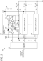
Fig. 2 is a diagram showing one example of the configuration of a general light-emitting device 20a. The light-emitting device 20a includes light sources D0 to D9, acapacitor 40,power supply circuits 50 to 59, and acontrol circuit 60. Note that inFig. 2 , for the sake of convenience, part of the configuration (light sources D2 to D8, power supply circuits 52 to 58) of the light-emitting device 20a is omitted. - The light source D0 includes, for example, a surface emitting laser (vertical cavity surface emitting laser) capable of emitting measurement light in an infrared range. Specifically, as in an example shown in
Fig. 3 , the light source D0 includes, for example, 16laser diodes 100 to 115 and anoptical member 120 that adjusts distribution of light from thelaser diodes 100 to 115. - The cathodes of the
laser diodes 100 to 115 are common, and the anodes are also common. Thus, the light emitted from each of thelaser diodes 100 to 115 is the measurement light from one light source D0. Note that the light source D0 includes the 16laser diodes 100 to 115 here, but may include another number (for example, 8 or 32) of laser diodes. - The
optical member 120 is, for example, a light shaping diffuser (LSD), and is a member that diffuses (i.e., adjusts) the light emitted from each of thelaser diodes 100 to 115 such that desired light distribution of the light from the light source D0 is obtained. Note that the LSD is used as theoptical member 120 here, but any member may be used as long as the light distribution of the light from the light source D0 can be in a desired pattern. - Since each of the light sources D1 to D9 includes the same surface emitting laser (hereinafter, simply referred to as "VCSEL") and the same
optical member 120 as those of the light source D0, detailed description thereof is omitted here. The nine light sources D0 to D9 correspond to "n (n is an integer of 2 or more)" light sources. In addition, hereinafter, the light source D0 may be described as a VCSEL for the sake of convenience. - The
capacitor 40 is an element that stabilizes a predetermined power supply voltage Vdd1 (e.g., several tens of V) supplied to thepower supply circuits 50 to 59. The predetermined power supply voltage Vdd1 is applied to thecapacitor 40. - The
power supply circuit 50 is a circuit that generates a power supply voltage V0 for turning on the light source D0 on the basis of the power supply voltage Vdd1 and a signal S0 from thecontrol circuit 60. Specifically, thepower supply circuit 50 generates the power supply voltage V0 when a high-level (hereinafter, "H-level") signal S0 is input from thecontrol circuit 60 to turn on the light source D0. On the other hand, thepower supply circuit 50 stops generating the power supply voltage V0 when a low-level (hereinafter, "L-level") signal S0 is input from thecontrol circuit 60 to turn off the light source D0. - The
power supply circuit 50 includes adiode 200, acapacitor 201, abuffer 210, atransformer 211, an integrated circuit (IC) 212, and aresistor 213. - The
diode 200 is an element that generates a power supply voltage for operating the IC 212 (described later) together with thecapacitor 201. A power supply voltage Vdd2 (e.g., 5 V) is applied to the anode of thediode 200, and the cathode of thediode 200 is connected to thecapacitor 201. - When the
capacitor 201 is charged with the current from thediode 200, the power supply voltage for operating theIC 212 is generated. - The
buffer 210 outputs a signal Sa0 having the same logic level as that of the signal S0 to thetransformer 211. Specifically, thebuffer 210 outputs the H-level signal Sa0 on the basis of the H-level signal S0, and outputs the L-level signal Sa0 on the basis of the L-level signal S0. Here, the signal S0 is a signal for controlling ON/OFF of a driving transistor 231 (described later) of theIC 212, the L-level of the signal S0 is, for example, 0 V, and the H-level is, for example, 3 V. - The
transformer 211 is an isolated transformer that converts and outputs a DC level while maintaining the amplitude of an input signal, and includes aprimary coil 220 and asecondary coil 221 electromagnetically coupled to theprimary coil 220. - Here, the
transformer 211 functions as a so-called level shift circuit. Thus, thetransformer 211 converts the signal Sa0 of which the logic level changes with reference to a ground voltage (0 V) into a signal Sb0 changing with reference to the power supply voltage V0. That is, thetransformer 211 causes thesecondary coil 221 to generate the H-level signal Sb0 when the signal Sa0 is at the H-level, and causes thesecondary coil 221 to generate the L-level signal Sb0 when the signal Sa0 is at the L-level. - Here, the
transformer 211 is used as the so-called level shift circuit, but the present invention is not limited thereto and other configurations (e.g., circuit including a photocoupler) may be used. - The
IC 212 generates the power supply voltage V0 to the light source D0 when the signal Sb0 from thesecondary coil 221 is at the H-level, and stops generating the power supply voltage V0 when the signal Sb0 is at the L-level. TheIC 212 includes abuffer 230 and the drivingtransistor 231. - The
buffer 230 outputs a signal having the same logic level as that of the signal Sb0 to the drivingtransistor 231. Specifically, when the H-level signal Sb0 is output from thesecondary coil 221, thebuffer 230 outputs the H-level signal to the drivingtransistor 231. As a result, the drivingtransistor 231 is turned on. - On the other hand, when the L-level signal Sb0 is output from the
secondary coil 221, thebuffer 230 outputs the L-level signal to the drivingtransistor 231. As a result, the drivingtransistor 231 is turned off. - Here, when the driving
transistor 231 is turned on, the power supply voltage V0 of a line L0 on the anode side of the light source D0 increases to almost the power supply voltage Vdd1. Since the high-level power supply voltage V0 is applied to the line L0 on the anode side of the light source D0, the light source D0 is turned on (emits the measurement light). - Note that the
resistor 213 is an element for limiting the current flowing through the light source D0. When the drivingtransistor 231 is turned on, the voltage of the line L0 to which the source electrode of the drivingtransistor 231 is connected increases to almost the power supply voltage Vdd1 (e.g., several tens of V). Thus, in order to maintain the ON state of the drivingtransistor 231, it is necessary to continuously apply a voltage higher than the threshold of the drivingtransistor 231 from the voltage of the line L0 to the gate electrode of the drivingtransistor 231. - In the
power supply circuit 50 ofFig. 2 , thetransformer 211 shifts the DC level of the signal Sa0, and outputs the signal Sb0 to the secondary side. Thus, the logic level (H-level or L-level) of the signal Sb0 on the secondary side of thetransformer 211 changes with reference to the voltage of the line L0. As a result, in thepower supply circuit 50, ON/OFF of the drivingtransistor 231 can be controlled on the basis of the signal S0 changing with reference to the ground voltage (0 V). - Note that when the signal S0 changes to the L-level and the driving
transistor 231 is turned off, thepower supply circuit 50 stops generating the power supply voltage V0. As a result, the supply of the power supply voltage V0 to the light source D0 is also stopped, and therefore, the light source D0 is turned off. - Similarly to the
power supply circuit 50, each of thepower supply circuits 51 to 59 generates a power supply voltage V1 to V9 for the light source D1 to D9 on the basis of a signal S1 to S9. Thus, detailed description of thepower supply circuits 51 to 59 is omitted here. - The
control circuit 60 controls each of thepower supply circuits 50 to 59 such that the light sources D0 to D9 are sequentially turned on on the basis of a light-on start instruction from thecontrol device 22 ofFig. 1 . Here, "the light sources D0 to D9 are sequentially turned on" means that, for example, the ten light sources D0 to D9 are turned on one by one in the order of the light sources D0, D1,..., and D9. Thus, for example, when the light source D0 of the light sources D0 to D9 is turned on, the other light sources D1 to D9 are turned off, and for example, when the light source D1 is turned on, the light sources D0, D2 to D9 are turned off. - Thus, the
control circuit 60 sets the level of one signal corresponding to the light source to be turned on among the signals S0 to S9 to the H-level, and sets the levels of the other nine signals to the L-level. By outputting such signals S0 to S9, the light sources D0 to D9 are sequentially turned on. - Meanwhile, each of the
power supply circuits 50 to 59 of the light-emittingdevice 20a ofFig. 2 includes many components such as thetransformer 211 and theIC 212. For this reason, in general, a mounting space occupied by thepower supply circuits 50 to 59 in the light-emittingdevice 20a is wide. - In addition, the
transformer 211 that shifts the level of the signal S0 and thecapacitor 201 that generates the power supply voltage for thebuffer 230 include a relatively-large parasitic inductor or parasitic capacitance, the accuracy of the power supply voltage V0 for the light source D0 may be degraded. For this reason, in themeasurement device 10 of the present embodiment, a light-emittingdevice 20b operating with a simple configuration is used. - The light-emitting
device 20b shown inFig. 4 is a device that turns on the light sources D0 to D9 on the basis of the light-on start instruction from thecontrol device 22, and includes the light sources D0 to D9, thecapacitor 40, anIC 41,power supply circuits 70 to 79, and acontrol circuit 80. Note that the components denoted by the same reference numerals inFig. 4 andFig. 2 are the same as each other. Thus, theIC 41, thepower supply circuits 70 to 79, and thecontrol circuit 80 will be mainly described. Note that inFig. 4 , for the sake of convenience, part of the configuration (light sources D2 to D8, power supply circuits 72 to 78) of the light-emittingdevice 20b is omitted. - The
IC 41 is a circuit that turns on the light source to which the power supply voltage is applied among the light sources D0 to D9. TheIC 41 of the present embodiment is provided between the ground-side node of each of the light sources D0 to D9 and the ground. Note that the "ground-side node of the light source D0" is, for example, a node to which the cathodes of thelaser diodes 100 to 115 forming the light source D0 are connected. - The
IC 41 is a circuit similar to theIC 212 ofFig. 2 , and includes abuffer 300 and a drivingtransistor 301. - Similarly to the
buffer 230, thebuffer 300 outputs a signal having the same logic level as that of the input signal to the drivingtransistor 301. In the present embodiment, a signal S20 from the control circuit 80 (described later) is input to thebuffer 300. Thus, thebuffer 300 turns on the drivingtransistor 301 on the basis of the H-level signal S20, and turns off the drivingtransistor 301 on the basis of the L-level signal S20. - Note that the H-level signal S20 corresponds to a "light-on instruction" for turning on the light source, and the L-level signal S20 corresponds to a "light-off instruction" for turning off the light source.
- Of the driving
transistor 301, the drain electrode is connected to the ground-side nodes of the light sources D0 to D9, and the source electrode is grounded. Thus, when the drivingtransistor 301 is turned on, a current flows through the light source to which the power supply voltage is applied among the light sources D0 to D9, and such a light source is turned on. Note that when the drivingtransistor 301 is turned off, the path of the current from the light sources D0 to D9 to the ground is cut off, and all the light sources D0 to D9 are turned off. - The driving
transistor 301 of the present embodiment corresponds to a "switch." Note that in the present embodiment, as the "switch," an N-type field effect transistor (FET) of gallium nitride (Ga) is used for the drivingtransistor 301, but for example, another compound transistor or a general MOS transistor or bipolar transistor may be used. - The
power supply circuit 70 is a circuit that generates a power supply voltage V10 for turning on the light source D0 on the basis of a signal S10. Specifically, thepower supply circuit 70 generates the power supply voltage V10 when the H-level signal S10 is input, and stops generating the power supply voltage V10 when the L-level signal S10 is input. - The
power supply circuit 70 includes abuffer 310, aPMOS transistor 311, an NMOS transistor 312, aresistor 313, and acapacitor 314. - The
buffer 310 operates as an inverter that outputs a signal Sc0 obtained by inverting the logic level of the signal S10. Thus, thebuffer 310 outputs the L-level signal Sc0 on the basis of the H-level S10, and outputs the H-level signal Sc0 on the basis of the L-level S10. - The gate electrode of the
PMOS transistor 311 is connected to the gate electrode of the NMOS transistor 312, and the drain electrode of thePMOS transistor 311 is connected to the drain electrode of the NMOS transistor 312. Thus, thePMOS transistor 311 and the NMOS transistor 312 form a so-called push-pull circuit. - In the present embodiment, when the signal Sc0 changes to the L-level, the
PMOS transistor 311 is turned on, and the NMOS transistor 312 is turned off. As a result, thecapacitor 314 is charged, and increases to almost the power supply voltage Vdd1 (e.g., several tens of V). - When the signal Sc0 changes to the H-level, the
PMOS transistor 311 is turned off, and the NMOS transistor 312 is turned on. Thus, thecapacitor 314 is discharged. Note that at this time, the charge voltage of thecapacitor 314 decreases to almost 0 V. - Here, in the present embodiment, one end of the
capacitor 314 is connected to the anode of the light source D0 via a line L10. Thus, the charge voltage of thecapacitor 314 is the power supply voltage V10 generated by thepower supply circuit 70. - In this manner, the
power supply circuit 70 can generate the power supply voltage V10 for turning on the light source D0 or stop generating the power supply voltage V10 on the basis of the logic level of the signal S10. - Note that in the present embodiment, the
buffer 310, thePMOS transistor 311, and the NMOS transistor 312 correspond to a "charge-discharge circuit" that charges and discharges thecapacitor 314. Theresistor 313 provided between the above-described push-pull circuit and thecapacitor 314 is an element that limits a current for charging and discharging thecapacitor 314. Further, thepower supply circuit 70 corresponds to a circuit that generates the power supply voltage V10 for "one corresponding light source D0" among the light sources D0 to D9. Thecapacitor 314 corresponds to a "first capacitor." - Similarly to the
power supply circuit 70, each of thepower supply circuits 71 to 79 generates a power supply voltage V11 to V19 for the light source D11 to D19 on the basis of a signal S11 to S19. Thus, detailed description of thepower supply circuits 71 to 79 is omitted here. Note that in the present embodiment, thepower supply circuits 70 to 79 are each provided for the light sources D0 to D9. - The
control circuit 80 controls each of thepower supply circuits 70 to 79 such that the light sources D0 to D9 are sequentially turned on on the basis of the light-on start instruction from thecontrol device 22 ofFig. 1 . Specifically, thecontrol circuit 80 sets the level of the signal for the power supply circuit corresponding to the light source to be turned on among the signals S10 to S19 to the H-level, and sets the levels of the other nine signals to the L-level. - In addition, when the light-on start instruction is input, the
control circuit 80 outputs the H-level signal S20 (light-on instruction) at the timing of turning on the target light source, and outputs the L-level signal S20 (light-off instruction) at the timing of turning off the target light source. -
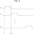
Fig. 5 is a chart showing one example of the waveforms of the signals S10 to S19.Fig. 6 is a chart showing one example of a main waveform of the light-emittingdevice 20b when the light source D0 is turned on. Note that inFig. 5 , only the signals S10, S11, S19 are shown for the sake of convenience. - First, the
control circuit 80 ofFig. 4 changes the signal S10 from the L-level to the H-level at time t0, and thus thepower supply circuit 70 starts generating the power supply voltage V10. As a result, as shown inFig. 6 , the power supply voltage V10 increases from 0 V to the level of the power supply voltage Vdd1. Note that in practice, the power supply voltage V10 increases slightly after the rising timing t0 of the signal S10, but here, such a delay is omitted for the sake of convenience. - Further, the
control circuit 80 sets each of the signals S11 to S19 to the L-level at the time t0. Thus, generation of the power supply voltages V11 to VB19 of thepower supply circuits 71 to 79 is stopped. - At time t1 (see
Fig. 6 ) when a predetermined period Ta has elapsed from the time t0, thecontrol circuit 80 outputs the H-level signal S20 to turn on the light source D0. As a result, the drivingtransistor 301 of theIC 41 ofFig. 4 is turned on. Thus, a current I0 flows through the light source D0, and the light source D0 is turned on. - Note that in the present embodiment, the predetermined period Ta is a period longer than a period from when the level of the power supply voltage V10 is 0 V to when the level changes to the power supply voltage Vdd1. When the current I0 flows through the light source D0, the
capacitor 40 is discharged, and therefore, the power supply voltage V10 decreases from the level of the power supply voltage Vdd1. - Then, at time t2 in
Fig. 6 , thecontrol circuit 80 changes the signal S20 to the L-level in order to turn off the light source D0. As a result, the drivingtransistor 301 is turned off. The current I0 for the light source D0 is cut off, and therefore, the light source D0 is turned off. Note that at the time t2, the current I0 is cut off and discharge of thecapacitor 40 is stopped, and therefore, the power supply voltage V10 increases to the power supply voltage Vdd1. - Then, at time t3, the
control circuit 80 changes the signal S20 to the H-level, and therefore, the light source D0 is turned on again. Note that in the present embodiment, the operation from the time t1 to the time t2 is repeated four times after the time t3. Note that while the power supply voltage V10 is being generated, the light source D0 is turned on five times, but the number of times of turning on the light source D0 is one example. - At time t11, the
control circuit 80 changes the signal S10 to the L-level in order to stop generating the power supply voltage V10. As a result, thecapacitor 314 ofFig. 4 is discharged via theresistor 313 and the NMOS transistor 312, and therefore, the power supply voltage V10 gradually decreases. Note that in practice, the power supply voltage V10 decreases slightly after the falling timing t11 of the signal S10, but here, such a delay is omitted for the sake of convenience. - As shown in
Fig. 5 , at the time t11, thecontrol circuit 80 changes the signal S11 to the H-level in order to generate the power supply voltage V11. As a result, the capacitor 314 (not shown) of thepower supply circuit 71 is gradually charged, and therefore, the power supply voltage V11 increases. - Note that in the present embodiment, for example, as shown at the time t11 in
Fig. 5 , the timing of starting discharging thecapacitor 314 of thepower supply circuit 70 is the same as the timing of starting charging the capacitor 314 (not shown) of thepower supply circuit 71. That is, in the present embodiment, thecontrol circuit 80 controls thepower supply circuits power supply circuit 71 is charged when thecapacitor 314 of thepower supply circuit 70 is discharged. - It is also possible to start charging the capacitor 314 (not shown) of the
power supply circuit 71 after thecapacitor 314 of thepower supply circuit 70 has been discharged and the power supply voltage V10 gas become almost 0 V. However, in such a case, the signal S11 changes to the H-level after time t12 inFigs. 5 and6 , and therefore, the timing of turning on the light source D1 is also delayed. - In the present embodiment, when the
capacitor 314 of thepower supply circuit 70 is discharged (i.e., in a period in which the level of the power supply voltage V10 decreases and is higher than 0 V), charge of thecapacitor 314 of thepower supply circuit 71 to be turned on next is started. Thus, in the present embodiment, the light source can be turned on at shorter intervals. - Although not shown in
Fig. 5 , when the above-described predetermined period Ta has elapsed from the time t11, thecontrol circuit 80 outputs the H-level signal S20 five times as in a case where the predetermined period Ta has elapsed from the time t0 (seeFig. 6 ). As a result, the light source D1 is also turned on five times at the same timing as that of the light source D0. Here, the operation when thecontrol circuit 80 turns on the light sources D0, D1 has been described, but the same also applies to the other light sources D2 to D9. - As described above, the
power supply circuit 70 of the present embodiment inFig. 4 does not include thediode 200, thecapacitor 201, thetransformer 211, and theIC 212 included in thepower supply circuit 50 ofFig. 2 . Further, the light-emittingdevice 20b controls ON/OFF of the light sources D0 to D9 by providing oneIC 41 between the ground-side nodes of the light sources D0 to D9 and the ground. Thus, in the present embodiment, ON of the plurality of light sources can be controlled with a simple configuration. - Note that the H-level signals S10 to S19 of the present embodiment correspond to a "first signal," and the L-level signals S10 to S19 correspond to a "second signal." Further, for example, the
power supply circuit 70 corresponds to a "first power supply circuit," and thepower supply circuit 71 corresponds to a "second power supply circuit." - In order to increase the distance (hereinafter, referred to as a "measurement distance") to the
object 11, which can be measured by themeasurement device 10, it is necessary to strengthen the light emitted from the light source D0. In addition, in order to strengthen the light emitted from the light source D0, it is necessary to increase the current I0 for turning on the light source D0. As described above, in the light-emittingdevice 20b ofFig. 4 , the discharge current for thecapacitor 314 of thepower supply circuit 70 is the current I0 for turning on the light source D0. Thus, when the capacity of thecapacitor 314 is increased, the measurement distance of themeasurement device 10 can be increased. - Note that when the capacity of the
capacitor 314 is increased, a variation between thecapacitors 314 included in thepower supply circuits 70 to 79 generally increases.Fig. 7 is a graph showing one example of the waveforms of the currents I0 to I2 when the capacities of thecapacitors 314 of thepower supply circuits 70 to 72 are 2200 pF, 2000 pF, and 1800 pF, respectively. - Note that in
Fig. 7 , the current I0 from thecapacitor 314 of 2200 pF is indicated by a solid line, the current I1 from thecapacitor 314 of 2000 pF is indicated by a wide dotted line, and the current I2 from thecapacitor 314 of 1800 pF is indicated by a narrow dotted line. - In addition, in
Fig. 7 , the timing of turning on the drivingtransistor 301 when the currents I0 to I2 are generated is drawn with reference to time t20 so that the waveforms of the currents I0 to I2 can be compared. - Here, the current I0 will be described as an example. Since the driving
transistor 301 is turned on at the time t20, the current I0 increases. Then, when thecapacitor 314 of thepower supply circuit 70 is discharged, the current I0 decreases to zero. Thereafter, the drivingtransistor 301 is turned off at predetermined timing. Note that although the current I0 has been described as an example here, the same also applies to the currents I1, I2. - In the present embodiment, as shown in
Fig. 7 , when the capacity of thecapacitor 314 is as large as 2200 pF, the peak value (approximately 18 A) of the current I0 for turning on the light source is larger than the peak value (approximately 17.5 A, approximately 17 A) of each of the current values I1 and I2. Thus, in the light-emittingdevice 20b, when thecapacitor 314 having a small variation is used in each of thepower supply circuits 70 to 79, the light sources D0 to D9 can be turned on with favorable accuracy. Note that by using a capacitor (e.g., capacitor smaller than 1000 pF) having a relatively-small capacity value for the plurality ofcapacitors 314, it is possible to reduce the variation between the plurality ofcapacitors 314. - A light-emitting
device 20c shown inFig. 8 is a device capable of reducing the variation in the currents I0 to I9 while increasing the peak values of the currents I0 to I9. The light-emittingdevice 20c includes the light sources D0 to D9, thecapacitors IC 41, thepower supply circuits 70 to 79, thecontrol circuit 80, and aresistor 401. Note that the components denoted by the same reference numerals inFig. 8 andFig. 4 are the same as each other. Thus, thecapacitor 400, theresistor 401, and thecapacitor 314 included in each of thepower supply circuits 70 to 79 will be mainly described here. - The
capacitor 400 is an element for determining the current values (particularly, peak values) of the currents I0 to I9 for turning on the light sources D0 to D9, and is provided between the ground-side node of each of the light sources D0 to D9 and the drivingtransistor 301. Specifically, one end of thecapacitor 400 is connected to the ground-side node of each of the light sources D0 to D9, and the other end is connected to the drain electrode of the drivingtransistor 301. - The
resistor 401 is an element that discharges the electric charge of thecapacitor 400. Of theresistor 401, one end is connected to the ground-side node of each of the light sources D0 to D9, and the other end is connected to the drain electrode of the drivingtransistor 301. Thus, theresistor 401 is connected in parallel to thecapacitor 400. Note that thecapacitor 400 corresponds to a "second capacitor." - Here, the waveform of the current flowing through the light source of the light-emitting
device 20c will be described. In the present embodiment, the capacity of thecapacitor 400 is, for example, 2000 pF, and a capacitor (e.g., 0.1 µF) sufficiently larger in a capacity than 2000 pF is used for thecapacitor 314 of each of thepower supply circuits 70 to 79. - Note that there is the variation between the
capacitors 314 of thepower supply circuits 70 to 79. In the present embodiment, it is assumed that the capacity of thecapacitor 314 of thepower supply circuit 70 is, for example, 0.11 µF, the capacity of thecapacitor 314 of thepower supply circuit 71 is, for example, 0.1 µF, and the capacity of thecapacitor 314 of the power supply circuit 72 is, for example, 0.09 µF. - Further, the currents I0 to I2 flowing through the light sources D0 to D2 will be described here with reference to
Fig. 9 . Note that inFig. 9 , the current I0 is indicated by a solid line, the current I1 is indicated by a wide dotted line, and the current I2 is indicated by a narrow dotted line. Although details will be described later, in the present embodiment, the waveforms of the currents I0 to I2 are substantially the same as each other, and therefore, three current waveforms overlap with each other inFig. 9 . - In a state in which the
power supply circuit 70 ofFig. 8 generates the power supply voltage V10 (i.e., the signal S10 is in the H-level state), for example, when the signal S20 changes to the H-level at time t30 inFig. 9 , the drivingtransistor 301 is turned on. - As a result, the
capacitor 314 of thepower supply circuit 70 is discharged, and the charge current for charging thecapacitor 400 increases. In the present embodiment, the charge current for thecapacitor 400 is the current I0 for turning on the light source D0, and therefore, the current I0 increases. - Thereafter, the
capacitor 400 is gradually charged, and when the current I0 reaches the peak value, the current I0 decreases. Then, the dischargedcapacitor 314 is charged, and therefore, the current I0 decreases to almost zero. Thereafter, the drivingtransistor 301 is turned off at predetermined timing. Note that when the drivingtransistor 301 is turned off, thecapacitor 400 is discharged via theresistor 401. - Here, the current I0 when the
power supply circuit 70 generates the power supply voltage V10 has been described. However, as shown inFig. 9 , the waveforms of the currents I1, I2 when thepower supply circuits 71, 72 generate the power supply voltages V11, V12 are also the charge current for thecapacitor 400. Thus, as shown inFig. 9 , the currents I0 to I2 have substantially the same waveform. - As described above, in the light-emitting
device 20c, when the capacity of thecapacitor 314 included in each of thepower supply circuits 70 to 79 is sufficiently larger than the capacity of thecapacitor 400, the waveforms and peak values of the currents I0 to I9 are determined by the capacity of thecapacitor 400. Thus, in the light-emittingdevice 20c, even when the measurement distance is increased, the variation in the currents I0 to I9 can be reduced. - Note that when the measurement distance is relatively short, the capacity of each of the plurality of
capacitors 314 of thepower supply circuits 70 to 79 in the light-emittingdevice 20b ofFig. 4 can be decreased. In such a case, the variation between the plurality ofcapacitors 314 of thepower supply circuits 70 to 79 is also generally reduced, and therefore, the variation in the intensity of the light emitted from the light sources D0 to D9 is also reduced. Thus, when the measurement distance is relatively short, the light-emittingdevice 20b can be used. - In the present embodiment, the VCSEL is used for each of the light sources D0 to D9, but the present invention is not limited thereto and, for example, a light emitting diode may be used. Even when the light emitting diodes are used as the light sources D0 to D9, a light-emitting device can be provided with a simple configuration as in the present embodiment.
- The
measurement device 10 of the present embodiment has been described above. In the light-emittingdevice 20b, the drivingtransistor 301 is provided between the ground-side nodes of the light sources D0 to D9 and the ground. Thus, when the drivingtransistor 301 is turned on while the power supply voltage is being supplied to the target light source, the target light source can be turned on. Consequently, the light-emittingdevice 20b can turn on the plurality of light sources with a simple configuration with a less number of components. - Further, in the light-emitting
device 20b, for example, when thepower supply circuit 70 generates the power supply voltage V10, thepower supply circuits 71 to 79 discharge the capacitors 314 (not shown) therein. Thus, when the drivingtransistor 301 is turned on, only a desired light source of the plurality of light sources can be turned on. In addition, when the measurement distance is relatively short, the variation between thecapacitors 314 of thepower supply circuits 71 to 79 is reduced. Thus, in such a case, the light-emittingdevice 20b can be used. - In the
power supply circuit 70, theresistor 313 is provided between thecapacitor 314 and the push-pull circuit including thePMOS transistor 311 and the NMOS transistor 312. Thus, the charge current and discharge current for thecapacitor 314 can be limited to appropriate current values. Further, as a component forming thepower supply circuit 70, a low power type component can be used as compared with a component forming thepower supply circuit 50. - For example, as shown in
Figs. 4 and5 , thecontrol circuit 80 controls thepower supply circuits power supply circuit 71 is charged when thecapacitor 314 of thepower supply circuit 70 is discharged. That is, in the present embodiment, generation of the power supply voltage V11 is started before the power supply voltage V10 reaches 0 V, and therefore, the light source D1 can be smoothly turned on after the light source D0 has been turned off. - In the light-emitting
device 20c, thecapacitor 400 and theresistor 401 are provided between the light sources D0 to D9 and the drivingtransistor 301. Thus, in the light-emittingdevice 20c, the charge current for thecapacitor 400 is the currents I0 to I9, and therefore, the variation in the currents I0 to I9 can be reduced. - In the light-emitting
device 20c, the capacity of thecapacitor 314 of each of thepower supply circuits 70 to 79 is larger than the capacity of thecapacitor 400. Thus, thecapacitor 314 can supply a sufficient current to thecapacitor 400. - For example, in the light-emitting
device 20c, the capacity of thecapacitor 400 is, for example, 1000 pF or more. As a result, in the light-emittingdevice 20c, the peak values of the currents I0 to I9 can be increased so that the measurement distance can be increased. - Although the VCSEL can be used as the light source D0, for example, a light emitting diode having a cathode and an anode may be used as in the VCSEL. In such a case, the light source D0 includes the light emitting diode and the
optical member 120. - The above-described embodiments are for the sake of easy understanding of the present invention, and are not intended to limit the present invention. In addition, the present invention can be changed or modified without departing from the gist thereof, and the present invention includes equivalents thereof, needless to say.
- The present international application claims priority based on
Japanese Patent Application No.2022-093042 Japanese Patent Application No.2022-112517 Japanese Patent Application No. 2022-093042 Japanese Patent Application No. 2022-112517 - The description of the specific embodiments of the present invention is presented for the purpose of illustration. The specific embodiments are not intended to be exhaustive or to limit the invention as it is in the form described. It is obvious to those skilled in the art that many modifications and alterations are possible in light of the contents of the description above.
-
- 10 Measurement Device
- 11 Object
- 20, 20a, 20b Light-Emitting Device
- 21 Light Receiving Device
- 22 Control Device
- 40, 201, 314, 400 Capacitor
- 41, 212 IC
- 50 to 59 Power Supply Circuit
- 60 Control Circuit
- 100 to 115 Laser Diode
- 120 Optical Member
- 200 Diode
- 210, 230, 300, 310 Buffer
- 211 Transformer
- 213, 313, 401 Resistor
- 220 Primary Coil
- 221 Secondary Coil
- 231, 301Driving Transistor
- 312 NMOS Transistor
- 311 PMOS Transistor
- D0 to D9 Light Source
Claims (8)
- A light-emitting device comprising:n (n ≥ 2) light sources;n power supply circuits each provided for the n light sources; anda switch provided between a ground-side node of each of the n light sources and a ground,wherein each power supply circuit generates a power supply voltage for a corresponding one of the n light sources on the basis of a first signal, and stops generating the power supply voltage on the basis of a second signal, andthe switch is turned on on the basis of a light-on instruction and is turned off on the basis of a light-off instruction when the power supply voltage for the one light source is generated.
- The light-emitting device according to claim 1, whereineach power supply circuit includesa first capacitor that generates the power supply voltage, anda charge-discharge circuit that charges the first capacitor on the basis of the first signal and discharges the first capacitor on the basis of the second signal.
- The light-emitting device according to claim 2, further comprising
a resistor provided between the charge-discharge circuit and the first capacitor. - The light-emitting device according to claim 3, further comprising:a control circuit that outputs the first and second signals to each of the n power supply circuits and controls each of the n power supply circuits,wherein the control circuitcontrols first and second power supply circuits of the n power supply circuits such that the first capacitor of the second power supply circuit is charged when the first capacitor of the first power supply circuit is discharged.
- The light-emitting device according to claim 2, further comprising:a second capacitor provided between the ground-side node of each of the n light sources and the switch; anda resistor connected in parallel to the second capacitor.
- The light-emitting device according to claim 5, wherein
a capacity of the first capacitor is larger than a capacity of the second capacitor. - The light-emitting device according to claim 6, wherein
the capacity of the second capacitor is 1000 pF or more. - The light-emitting device according to any one of claims 1 to 7, wherein
the light source includes any of a laser diode or a light emitting diode, and an optical member that adjusts distribution of light from the any of the laser diode or the light emitting diode.
Applications Claiming Priority (3)
| Application Number | Priority Date | Filing Date | Title |
|---|---|---|---|
| JP2022093042 | 2022-06-08 | ||
| JP2022112517A JP2023180193A (en) | 2022-06-08 | 2022-07-13 | light emitting device |
| PCT/JP2023/020615 WO2023238786A1 (en) | 2022-06-08 | 2023-06-02 | Light-emitting device |
Publications (2)
| Publication Number | Publication Date |
|---|---|
| EP4539270A1 true EP4539270A1 (en) | 2025-04-16 |
| EP4539270A4 EP4539270A4 (en) | 2025-09-17 |
Family
ID=89118288
Family Applications (1)
| Application Number | Title | Priority Date | Filing Date |
|---|---|---|---|
| EP23819766.9A Pending EP4539270A4 (en) | 2022-06-08 | 2023-06-02 | LIGHT-EMITTING DEVICE |
Country Status (4)
| Country | Link |
|---|---|
| US (1) | US20250338374A1 (en) |
| EP (1) | EP4539270A4 (en) |
| CN (1) | CN119325672A (en) |
| WO (1) | WO2023238786A1 (en) |
Family Cites Families (9)
| Publication number | Priority date | Publication date | Assignee | Title |
|---|---|---|---|---|
| JP6295778B2 (en) * | 2014-03-28 | 2018-03-20 | 富士通株式会社 | Optical semiconductor device and drive circuit control method |
| WO2016175301A1 (en) * | 2015-04-30 | 2016-11-03 | 株式会社トプコン | Light-emitting device and distance measurement device |
| US10511142B2 (en) * | 2017-05-03 | 2019-12-17 | Analog Modules, Inc. | Pulsed laser diode drivers and methods |
| JP2020038855A (en) * | 2018-08-31 | 2020-03-12 | ソニーセミコンダクタソリューションズ株式会社 | Light source device, adjustment method, and sensing module |
| US11240894B2 (en) * | 2018-11-30 | 2022-02-01 | Ricoh Company, Ltd. | Drive circuit, light emitting device, distance measurement apparatus, and mobile body |
| JP7275984B2 (en) | 2019-08-09 | 2023-05-18 | オムロン株式会社 | drive circuit |
| JP7467657B2 (en) * | 2020-03-02 | 2024-04-15 | 華為技術有限公司 | Depth Acquisition Components and Electronic Devices |
| JP7523339B2 (en) | 2020-12-11 | 2024-07-26 | 日立建機株式会社 | Work Machine |
| JP7068729B1 (en) | 2021-01-21 | 2022-05-17 | 音羽電機工業株式会社 | Ground terminal separated SPD and ground unit |
-
2023
- 2023-06-02 US US18/871,216 patent/US20250338374A1/en active Pending
- 2023-06-02 EP EP23819766.9A patent/EP4539270A4/en active Pending
- 2023-06-02 CN CN202380044907.5A patent/CN119325672A/en active Pending
- 2023-06-02 WO PCT/JP2023/020615 patent/WO2023238786A1/en not_active Ceased
Also Published As
| Publication number | Publication date |
|---|---|
| WO2023238786A1 (en) | 2023-12-14 |
| CN119325672A (en) | 2025-01-17 |
| US20250338374A1 (en) | 2025-10-30 |
| EP4539270A4 (en) | 2025-09-17 |
Similar Documents
| Publication | Publication Date | Title |
|---|---|---|
| US11563303B2 (en) | Optical pulse emitter | |
| US8169163B2 (en) | Control device and LED light emitting device using the control device | |
| US8098023B2 (en) | Driving circuit for and semiconductor device for driving laser diode | |
| CN113206589B (en) | Light source system | |
| GB2371429A (en) | A constant current OLED array driver with an auto-clamped precharge circuit | |
| US8519747B2 (en) | Driver and high voltage drive circuit including the same | |
| US20220069545A1 (en) | Controlling optical pulse shape of a laser diode | |
| US9917415B2 (en) | Driving circuit for light emitting element | |
| US7288978B2 (en) | Delay circuit and ring oscillator using the same | |
| JP4376385B2 (en) | Light emitting element drive circuit | |
| US11294055B2 (en) | Driving circuit to generate a signal pulse for operating a light-emitting diode | |
| US7626429B2 (en) | Driving circuit to drive an output stage | |
| US11482836B2 (en) | Laser diode driver circuits and methods of operating thereof | |
| US20250338374A1 (en) | Light-emitting device | |
| US20220408528A1 (en) | Light emitting element driving circuit and light emitting device | |
| CN114527472B (en) | Laser distance measuring controller and laser distance measuring equipment | |
| US12149048B2 (en) | Configurable high-frequency pulsed laser diode driver capacitor refresh circuit | |
| JP2023180193A (en) | light emitting device | |
| CN111341259B (en) | Shift register circuit | |
| KR20230133004A (en) | Laser driver for driving vcsel | |
| JPH0621540A (en) | Light emitting element driving circuit | |
| US7671854B2 (en) | High-potential output stage | |
| Ma et al. | A 30–110V Resonant Buck-Boost Power-Bus Charger Achieving 50-A Peak Laser-Current Pulse Generation in 2ns for MHz-Frequency Automotive LiDAR Transmitter | |
| US20240322822A1 (en) | Semiconductor device | |
| WO2024235794A1 (en) | Driver circuit and driving method |
Legal Events
| Date | Code | Title | Description |
|---|---|---|---|
| STAA | Information on the status of an ep patent application or granted ep patent |
Free format text: STATUS: THE INTERNATIONAL PUBLICATION HAS BEEN MADE |
|
| PUAI | Public reference made under article 153(3) epc to a published international application that has entered the european phase |
Free format text: ORIGINAL CODE: 0009012 |
|
| STAA | Information on the status of an ep patent application or granted ep patent |
Free format text: STATUS: REQUEST FOR EXAMINATION WAS MADE |
|
| 17P | Request for examination filed |
Effective date: 20241127 |
|
| AK | Designated contracting states |
Kind code of ref document: A1 Designated state(s): AL AT BE BG CH CY CZ DE DK EE ES FI FR GB GR HR HU IE IS IT LI LT LU LV MC ME MK MT NL NO PL PT RO RS SE SI SK SM TR |
|
| REG | Reference to a national code |
Ref country code: DE Ref legal event code: R079 Free format text: PREVIOUS MAIN CLASS: H01S0005042000 Ipc: G01S0007481000 |
|
| A4 | Supplementary search report drawn up and despatched |
Effective date: 20250819 |
|
| DAV | Request for validation of the european patent (deleted) | ||
| DAX | Request for extension of the european patent (deleted) | ||
| RIC1 | Information provided on ipc code assigned before grant |
Ipc: G01S 7/481 20060101AFI20250812BHEP Ipc: G01S 7/484 20060101ALI20250812BHEP Ipc: H01S 5/042 20060101ALN20250812BHEP Ipc: H01S 5/062 20060101ALN20250812BHEP Ipc: H01S 5/42 20060101ALN20250812BHEP |