EP4539257A1 - Connector and assembly - Google Patents
Connector and assembly Download PDFInfo
- Publication number
- EP4539257A1 EP4539257A1 EP24196856.9A EP24196856A EP4539257A1 EP 4539257 A1 EP4539257 A1 EP 4539257A1 EP 24196856 A EP24196856 A EP 24196856A EP 4539257 A1 EP4539257 A1 EP 4539257A1
- Authority
- EP
- European Patent Office
- Prior art keywords
- mating
- accommodating
- connector
- ditches
- contact
- Prior art date
- Legal status (The legal status is an assumption and is not a legal conclusion. Google has not performed a legal analysis and makes no representation as to the accuracy of the status listed.)
- Granted
Links
Images





Classifications
-
- H—ELECTRICITY
- H01—ELECTRIC ELEMENTS
- H01R—ELECTRICALLY-CONDUCTIVE CONNECTIONS; STRUCTURAL ASSOCIATIONS OF A PLURALITY OF MUTUALLY-INSULATED ELECTRICAL CONNECTING ELEMENTS; COUPLING DEVICES; CURRENT COLLECTORS
- H01R12/00—Structural associations of a plurality of mutually-insulated electrical connecting elements, specially adapted for printed circuits, e.g. printed circuit boards [PCB], flat or ribbon cables, or like generally planar structures, e.g. terminal strips, terminal blocks; Coupling devices specially adapted for printed circuits, flat or ribbon cables, or like generally planar structures; Terminals specially adapted for contact with, or insertion into, printed circuits, flat or ribbon cables, or like generally planar structures
- H01R12/70—Coupling devices
- H01R12/91—Coupling devices allowing relative movement between coupling parts, e.g. floating or self aligning
-
- H—ELECTRICITY
- H01—ELECTRIC ELEMENTS
- H01R—ELECTRICALLY-CONDUCTIVE CONNECTIONS; STRUCTURAL ASSOCIATIONS OF A PLURALITY OF MUTUALLY-INSULATED ELECTRICAL CONNECTING ELEMENTS; COUPLING DEVICES; CURRENT COLLECTORS
- H01R13/00—Details of coupling devices of the kinds covered by groups H01R12/70 or H01R24/00 - H01R33/00
- H01R13/40—Securing contact members in or to a base or case; Insulating of contact members
- H01R13/42—Securing in a demountable manner
- H01R13/422—Securing in resilient one-piece base or case, e.g. by friction; One-piece base or case formed with resilient locking means
-
- H—ELECTRICITY
- H01—ELECTRIC ELEMENTS
- H01R—ELECTRICALLY-CONDUCTIVE CONNECTIONS; STRUCTURAL ASSOCIATIONS OF A PLURALITY OF MUTUALLY-INSULATED ELECTRICAL CONNECTING ELEMENTS; COUPLING DEVICES; CURRENT COLLECTORS
- H01R12/00—Structural associations of a plurality of mutually-insulated electrical connecting elements, specially adapted for printed circuits, e.g. printed circuit boards [PCB], flat or ribbon cables, or like generally planar structures, e.g. terminal strips, terminal blocks; Coupling devices specially adapted for printed circuits, flat or ribbon cables, or like generally planar structures; Terminals specially adapted for contact with, or insertion into, printed circuits, flat or ribbon cables, or like generally planar structures
- H01R12/70—Coupling devices
- H01R12/71—Coupling devices for rigid printing circuits or like structures
- H01R12/712—Coupling devices for rigid printing circuits or like structures co-operating with the surface of the printed circuit or with a coupling device exclusively provided on the surface of the printed circuit
- H01R12/716—Coupling device provided on the PCB
-
- H—ELECTRICITY
- H01—ELECTRIC ELEMENTS
- H01R—ELECTRICALLY-CONDUCTIVE CONNECTIONS; STRUCTURAL ASSOCIATIONS OF A PLURALITY OF MUTUALLY-INSULATED ELECTRICAL CONNECTING ELEMENTS; COUPLING DEVICES; CURRENT COLLECTORS
- H01R12/00—Structural associations of a plurality of mutually-insulated electrical connecting elements, specially adapted for printed circuits, e.g. printed circuit boards [PCB], flat or ribbon cables, or like generally planar structures, e.g. terminal strips, terminal blocks; Coupling devices specially adapted for printed circuits, flat or ribbon cables, or like generally planar structures; Terminals specially adapted for contact with, or insertion into, printed circuits, flat or ribbon cables, or like generally planar structures
- H01R12/70—Coupling devices
- H01R12/71—Coupling devices for rigid printing circuits or like structures
- H01R12/72—Coupling devices for rigid printing circuits or like structures coupling with the edge of the rigid printed circuits or like structures
- H01R12/73—Coupling devices for rigid printing circuits or like structures coupling with the edge of the rigid printed circuits or like structures connecting to other rigid printed circuits or like structures
Definitions
- This invention relates to a connector which has at least two contact rows and a partition portion, and to an assembly.
- Patent Document 1 discloses a connector 900 of this type. As shown in Fig. 34 , the connector 900 of Patent Document 1 has a first housing 910, a fixed housing 920 and a plurality of first contacts 930, or contacts 930.
- the first housing 910 has a separation wall 912, or a partition portion 912.
- the contacts 930 form two contact rows.
- the partition portion 912 is positioned between the two contact rows in a Y-direction, or in a width direction.
- One aspect (first aspect) of the present invention provides a connector mateable along a mating direction with a mating connector which has a mating contact.
- the connector has an insulator and a plurality of contacts.
- the insulator holds the contacts.
- the insulator has a partition portion.
- the partition portion has opposite faces in a width direction perpendicular to the mating direction.
- the partition portion is formed with a plurality of accommodating ditches.
- the accommodating ditches are classified into two groups.
- the accommodating ditches of each of the groups are arranged in a pitch direction perpendicular to both the mating direction and the width direction.
- the accommodating ditches of one of the groups are positioned on one of the opposite faces of the partition portion.
- the accommodating ditches of a remaining one of the groups are positioned on a remaining one of the opposite faces of the partition portion.
- the accommodating ditches of one of the groups are different in position from the accommodating ditches of a remaining one of the groups in the pitch direction.
- Each of the accommodating ditches has a receiving portion. In the width direction, the receiving portion extends across a middle of the partition portion.
- the contacts correspond to the accommodating ditches, respectively.
- Each of the contacts is partially accommodated in the corresponding accommodating ditch.
- the contacts form two contact rows.
- Each of the contacts has a contact point and a distal end portion. The contact point is brought into contact with the mating contact when the connector and the mating connector are mated with each other.
- the receiving portion of each of the accommodating ditches is able to receive, at least in part, the distal end portion of the corresponding contact upon the mating of the connector with the mating connector.
- the mating connector comprises a mating insulator and a plurality of the mating contacts.
- the mating insulator holds the mating contacts.
- the mating insulator has two outer walls. Each of the outer walls extends in the pitch direction. Each of the outer walls is formed with a plurality of mating receiving portions. Each of the mating receiving portions pierces the outer wall in the width direction.
- the mating contacts form mating contact rows.
- the mating contact rows include an outermost contact row which is positioned outermost of the mating contact rows in the width direction.
- Each of the mating contacts has a mating distal end portion.
- the mating receiving portion is able to receive the mating distal end portion of the mating contact of the outermost contact row upon the mating of the connector with the mating connector.
- an assembly 10 according to a first embodiment of the present invention comprises a connector 100 and a mating connector 700.
- the mating connector 700 of the present embodiment is mateable with the connector 100 along a mating direction.
- the mating connector 700 of the present embodiment is a plug connector.
- the mating direction is a Z-direction.
- the mating direction is also referred to as an up-down direction. Specifically, it is assumed that upward is a positive Z-direction while downward is a negative Z-direction.
- the mating connector 700 of the present embodiment comprises a mating insulator 710 and a plurality of mating contacts 750.
- the mating insulator 710 of the present embodiment is made of insulator.
- the mating insulator 710 holds the mating contacts 750.
- the mating insulator 710 has two outer walls 720.
- each of the outer walls 720 of the present embodiment extends in a pitch direction.
- Each of the outer walls 720 has a flat-plate shape perpendicular to a width direction.
- the two outer walls 720 define opposite ends, respectively, of the mating insulator 710 in the width direction.
- Each of the outer walls 720 is formed with a plurality of mating receiving portions 722.
- the pitch direction is an X-direction.
- the width direction is a Y-direction.
- the width direction is also referred to as a front-rear direction. Specifically, it is assumed that forward is a positive Y-direction while rearward is a negative Y-direction.
- the mating insulator 710 has a partition portion accommodating portion 712.
- the partition portion accommodating portion 712 of the present embodiment is a space extending in the mating direction, or in the up-down direction.
- the partition portion accommodating portion 712 is opened downward in the up-down direction.
- each of the mating contacts 750 of the present embodiment is made of metal.
- Each of the mating contacts 750 is a spring contact.
- the mating contacts 750 form a plurality of mating contact rows 770.
- the mating contacts 750 form two of the mating contact rows 770.
- one of the two mating contact rows 770 which is positioned at a front of the mating connector 700, is referred to as a first mating contact row 771, while the other mating contact row 770 positioned at a rear of the mating connector 700 is referred to as a second mating contact row 772.
- the mating contact 750 of the first mating contact row 771 and the mating contact 750 of the second mating contact row 772 have the same shape as each other. However, the present invention is not limited thereto. Specifically, the mating contacts 750 may form three or more of the mating contact rows 770. The mating contacts 750 correspond to the mating receiving portions 722, respectively.
- each of the mating contacts 750 has a mating distal end portion 752.
- each of the mating receiving portions 722 is able to receive the mating distal end portion 752 of the corresponding mating contact 750 upon the mating of the connector 100 with the mating connector 700.
- the mating connector 700 should be configured as follows: the mating contact rows 770 include an outermost contact row which is positioned outermost of the mating contact rows 770 in the width direction; and the mating receiving portion 722 is able to receive the mating distal end portion 752 of the mating contact 750 of the outermost contact row upon the mating of the connector 100 with the mating connector 700.
- each of the mating contacts 750 has a mating contact point 754, a mating supporting portion 756, a mating held portion 757 and a mating fixed portion 758.
- the mating contact point 754 of the present embodiment faces inward in the width direction.
- the mating contact point 754 is positioned above the mating distal end portion 752 in the up-down direction.
- the mating supporting portion 756 of the present embodiment is positioned above the mating contact point 754 in the up-down direction.
- the mating supporting portion 756 extends downward in the up-down direction from the mating held portion 757.
- the mating supporting portion 756 is resiliently deformable.
- the mating contact point 754 is supported by the mating supporting portion 756.
- the mating supporting portion 756 resiliently supports the mating contact point 754. Accordingly, the mating contact point 754 is movable in the width direction.
- the mating fixed portion 758 of the present embodiment is fixed on a circuit board (not shown) by soldering or the like when the mating connector 700 is mounted on the circuit board.
- the mating fixed portion 758 extends outward in the width direction from the mating held portion 757.
- the mating fixed portion 758 defines an upper end of the mating contact 750 in the up-down direction.
- the mating fixed portion 758 defines an outer end of the mating contact 750 in the width direction.
- the connector 100 of the present embodiment is mateable along the mating direction with the mating connector 700 which has the mating contacts 750.
- the connector 100 of the present embodiment is a receptacle connector with a floating structure.
- the present invention is not limited thereto.
- the connector 100 may be a normal receptacle connector with no floating structure, or may be a plug connector.
- the connector 100 comprises an insulator 200 and a plurality of contacts 500.
- the movable housing 210 of the present embodiment has a partition portion 300.
- the insulator 200 has the partition portion 300.
- the partition portion 300 of the present embodiment has opposite faces 310 in the width direction.
- the opposite faces 310 include a front face 312 and a rear face 314.
- the front face 312 is positioned forward of the rear face 314 in the front-rear direction.
- the front face 312 is directed forward in the front-rear direction.
- the rear face 314 is directed rearward in the front-rear direction.
- the partition portion 300 is formed with a plurality of accommodating ditches 330.
- each of the accommodating ditches 330 of the present embodiment is recessed inward in the width direction.
- Each of the accommodating ditches 330 is opened upward in the up-down direction.
- Each of the accommodating ditches 330 is opened outward in the width direction.
- Each of the accommodating ditches 330 communicates with the accommodating portion 202 in the width direction.
- the accommodating ditches 330 are arranged in a staggered configuration.
- the accommodating ditches 330 are classified into two groups G1, G2.
- the number of the accommodating ditches 330 of the group G1 is equal to the number of the accommodating ditches 330 of the group G2.
- the accommodating ditches 330 of each of the groups G1, G2 are arranged in the pitch direction perpendicular to the mating direction.
- the accommodating ditches 330 of one of the groups G1, G2 correspond to the accommodating ditches 330, respectively, of a remaining one of the groups G1, G2.
- the accommodating ditches 330 of one of the groups G1, G2 are positioned on one of the opposite faces 310 of the partition portion 300.
- the accommodating ditches 330 of a remaining one of the groups G1, G2 are positioned on a remaining one of the opposite faces 310 of the partition portion 300.
- the accommodating ditches 330 of one of the groups G1, G2 are different in position from the accommodating ditches 330 of a remaining one of the groups G1, G2 in the pitch direction.
- Each of the accommodating ditches 330 of one of the groups G1, G2 occupies a first area in the pitch direction.
- Each of the accommodating ditches 330 of a remining one of the groups G1, G2 occupies a second area in the pitch direction.
- the first area of each of the accommodating ditches 330 of the one of the groups G1, G2 overlaps with the second area of one of the accommodating ditches 330 of the remining one of the groups G1, G2 in the pitch direction. More specifically, the first area of each of the accommodating ditches 330 of the one of the groups G1, G2 overlaps with the second area of the corresponding accommodating ditch 330 of the remining one of the groups G1, G2 in the pitch direction.
- the accommodating ditches 330 of the group G1 correspond to the accommodating ditches 330, respectively, of the group G2.
- the accommodating ditches 330 of the group G1 are positioned on the front face 312 of the partition portion 300.
- the accommodating ditches 330 of the group G2 are positioned on the rear face 314 of the partition portion 300.
- the accommodating ditches 330 of the group G1 are different in position from the accommodating ditches 330 of the group G2 in the pitch direction.
- Each of the accommodating ditches 330 of the group G1 occupies an area in the pitch direction.
- Each of the accommodating ditches 330 of the group G2 occupies another area in the pitch direction.
- each of the accommodating ditches 330 has a receiving portion 332.
- the receiving portion 332 extends across a middle 320 of the partition portion 300.
- the accommodating ditches 330 of the one of the groups G1, G2 are different in position from the accommodating ditches 330 of the remaining one of the groups G1, G2 in the pitch direction, and the receiving portion 332 extends across the middle 320 of the partition portion 300 in the width direction.
- the connector 100 of the present embodiment can have a reduced size in the width direction.
- the receiving portion 332 of each of the accommodating ditches 330 of the group G1 which is positioned on the front face 312 of the partition portion 300, extends across the middle 320 of the partition portion 300 toward the rear face 314 of the partition portion 300. It is noted that the receiving portion 332 of each of the accommodating ditches 330 of the group G1 does not reach the rear face 314 of the partition portion 300.
- the receiving portion 332 of each of the accommodating ditches 330 of the group G2 which is positioned on the rear face 314 of the partition portion 300, extends across the middle 320 of the partition portion 300 toward the front face 312 of the partition portion 300. It is noted that the receiving portion 332 of each of the accommodating ditches 330 of the group G2 does not reach the front face 312 of the partition portion 300.
- the receiving portion 332 has a narrow portion 3322 and a wide portion 3326.
- the insulator 200 of the present embodiment is configured so that each of the receiving portions 332 does not pierce the partition portion 300 in the width direction. Accordingly, molten resin can easily flow when the insulator 200 of the present embodiment is molded.
- the present invention is not limited thereto, but the receiving portion 332 may pierce the partition portion 300 in the width direction.
- the inner surface 3323 defines an inner end of the narrow portion 3322 in the width direction.
- the inner surface 3323 faces outward in the width direction.
- the inner surface 3323 is a plane perpendicular to the width direction.
- the inner surface 3323 of the receiving portion 332 of each of the accommodating ditches 330 of the group G1 is positioned rearward of the middle 320 of the partition portion 300 in the front-rear direction.
- the inner surface 3323 of the receiving portion 332 of each of the accommodating ditches 330 of the group G2 is positioned forward of the middle 320 of the partition portion 300 in the front-rear direction.
- the wide portion 3326 of the present embodiment is positioned outward of the narrow portion 3322 in the width direction.
- the wide portion 3326 defines an outer end of the receiving portion 332 in the width direction.
- a size of a part of the wide portion 3326 in the pitch direction decreases as the part approaches the narrow portion 3322.
- the wide portion 3326 couples the narrow portion 3322 and an additional receiving portion 334 with each other.
- the receiving portion 332 has a first surface 3324 facing in the mating direction.
- the first surface 3324 is oblique to both the mating direction and the width direction.
- the first surface 3324 faces upward in the up-down direction and outward in the width direction.
- the first surface 3324 extends upward in the up-down direction and inward in the width direction.
- each of the accommodating ditches 330 further has the additional receiving portion 334.
- the additional receiving portion 334 of the present embodiment is positioned below the receiving portion 332 in the up-down direction. Referring to Figs. 6 and 11 , the additional receiving portion 334 partially receives a supporting portion 540 upon the mating of the connector 100 with the mating connector 700. As shown in Fig. 19 , the additional receiving portion 334 has a second surface 3342 facing in the mating direction.
- the second surface 3342 is oblique to both the mating direction and the width direction.
- the second surface 3342 faces upward in the up-down direction and outward in the width direction.
- the second surface 3342 extends upward in the up-down direction and inward in the width direction.
- a first angle that the first surface 3324 makes with the mating direction is greater than a second angle that the second surface 3342 makes with the mating direction.
- An angle that the first surface 3324 makes with the width direction is smaller than an angle that the second surface 3342 makes with the width direction.
- the movable housing 210 has a plurality of first holding portions 212.
- Each of the first holding portions 212 is positioned around a lower end of the movable housing 210 in the up-down direction.
- Each of the first holding portions 212 is positioned below the partition portion 300 in the up-down direction.
- the movable housing 210 has a base portion 214.
- the base portion 214 defines the lower end of the movable housing 210 in the up-down direction.
- the partition portion 300 extends upward in the up-down direction from the base portion 214.
- the fixed housing 250 defines an outer end of the insulator 200 in a direction perpendicular to the mating direction.
- the fixed housing 250 defines opposite outer ends of the insulator 200 in the width direction perpendicular to the mating direction.
- the fixed housing 250 defines opposite outer ends of the insulator 200 in the pitch direction perpendicular to both the mating direction and the width direction.
- the partition portion 300 is surrounded by the fixed housing 250 in a plane perpendicular to the up-down direction.
- the fixed housing 250 has a plurality of second holding portions 252.
- Each of the second holding portions 252 is positioned around a lower end of the fixed housing 250 in the up-down direction.
- Each of the second holding portions 252 is positioned around an outer end of the fixed housing 250 in the width direction.
- the accommodating portion 202 of the present embodiment is opened upward in the up-down direction.
- the accommodating portion 202 is surrounded by the fixed housing 250 in the plane perpendicular to the up-down direction.
- the accommodating portion 202 accommodates a part of the mating connector 700 when the connector 100 and the mating connector 700 are mated with each other.
- first contact row 601 one of the contact rows 600, which is positioned at a front of the connector 100, is referred to as a first contact row 601
- the contact 500 of the first contact row 601 and the contact 500 of the second contact row 602 have the same shape as each other.
- the contacts 500 of the first contact row 601 correspond to the accommodating ditches 330, respectively, of the group G1.
- the contacts 500 of the second contact row 602 correspond to the accommodating ditches 330, respectively, of the group G2.
- Each of the contacts 500 of the first contact row 601 is partially accommodated in the corresponding accommodating ditch 330 of the group G1.
- Each of the contacts 500 of the second contact row 602 is partially accommodated in the corresponding accommodating ditch 330 of the group G2.
- each of the contacts 500 has a contact point 510 and a distal end portion 530.
- the contact point 510 of the present embodiment faces outward in the width direction.
- the contact point 510 is positioned in the accommodating portion 202.
- the narrow portion 3322 of the receiving portion 332 of each of the accommodating ditches 330 is smaller than the contact point 510 of the corresponding contact 500. That is, in the pitch direction, a size of the narrow portion 3322 of the receiving portion 332 of each of the accommodating ditches 330 is smaller than a size of the contact point 510 of the corresponding contact 500.
- the contact point 510 is brought into contact with the mating contact 750 when the connector 100 and the mating connector 700 are mated with each other.
- the receiving portion 332 of each of the accommodating ditches 330 is able to receive the distal end portion 530 of the corresponding contact 500 upon the mating of the connector 100 with the mating connector 700.
- the present invention is not limited thereto.
- the receiving portion 332 of each of the accommodating ditches 330 should be able to receive, at least in part, the distal end portion 530 of the corresponding contact 500 upon the mating of the connector 100 with the mating connector 700.
- the narrow portion 3322 of the receiving portion 332 of each of the accommodating ditches 330 receives a part of the distal end portion 530 of the corresponding contact 500 upon the mating of the connector 100 with the mating connector 700.
- the inner surface 3323 of the narrow portion 3322 of the receiving portion 332 of each of the accommodating ditches 330 is in non-contact with the distal end portion 530 of the corresponding contact 500 upon the mating of the connector 100 with the mating connector 700.
- each of the contacts 500 further has a guide portion 520.
- the guide portion 520 of the present embodiment extends upward in the up-down direction and inward in the width direction from the contact point 510.
- the guide portion 520 extends downward in the up-down direction and outward in the width direction from the distal end portion 530.
- the guide portion 520 couples the contact point 510 and the distal end portion 530 with each other.
- the guide portion 520 intersects with the mating direction, or with the up-down direction.
- the distal end portion 530 is smaller than the guide portion 520. That is, in the pitch direction, the size of the distal end portion 530 is smaller than a size of the guide portion 520.
- the guide portion 520 has a main portion 5202 and a tapered portion 5204.
- the main portion 5202 of the present embodiment defines an outer end of the guide portion 520 in the width direction.
- the main portion 5202 couples the contact point 510 and the tapered portion 5204 with each other.
- the main portion 5202 has a constant size in the pitch direction. In the pitch direction, the size of the main portion 5202 is greater than the size of the distal end portion 530.
- the tapered portion 5204 of the present embodiment defines an inner end of the guide portion 520 in the width direction.
- the tapered portion 5204 is coupled with the distal end portion 530.
- the tapered portion 5204 is tapered toward the distal end portion 530.
- each of the contacts 500 further has the supporting portion 540.
- the supporting portion 540 of the present embodiment is positioned below the contact point 510 in the up-down direction.
- the supporting portion 540 is resiliently deformable.
- the contact point 510 is supported by the supporting portion 540.
- the supporting portion 540 resiliently supports the contact point 510. Accordingly, the contact point 510 is movable in the width direction.
- each of the contacts 500 further has a fixed portion 550, a first held portion 560, a connection portion 570 and a second held portion 580.
- the fixed portion 550 of the present embodiment is fixed on a circuit board (not shown) by soldering or the like when the connector 100 is mounted on the circuit board.
- the fixed portion 550 extends outward in the width direction.
- the fixed portion 550 defines an outer end of the contact 500 in the width direction.
- the fixed portion 550 defines a lower end of the contact 500 in the up-down direction.
- the first held portion 560 of the present embodiment extends upward in the up-down direction from the connection portion 570. As shown in Fig. 11 , the first held portion 560 is held by the first holding portion 212. More specifically, the first held portion 560 is press-fit into the first holding portion 212.
- connection portion 570 of the present embodiment couples the first held portion 560 and the second held portion 580 with each other.
- the connection portion 570 is resiliently deformable.
- the movable housing 210 is movable relative to the fixed housing 250 in the plane perpendicular to the up-down direction by the resilient deformations of the connection portions 570.
- the second held portion 580 of the present embodiment extends upward in the up-down direction from the fixed portion 550.
- the second held portion 580 extends downward in the up-down direction from the connection portion 570.
- the second held portion 580 is held by the second holding portion 252. More specifically, the second held portion 580 is press-fit into the second holding portion 252.
- the structure of the contact 500 is not limited thereto.
- the contact 500 can be modified as described below.
- a contact 500A has a contact point 510, a guide portion 520A, a distal end portion 530A, a supporting portion 540, a fixed portion 550, a first held portion 560, a connection portion 570 and a second held portion 580.
- Components of the contact 500A other than the guide portion 520A and the distal end portion 530A have structures same as those of the aforementioned embodiment. Accordingly, a detailed description thereabout is omitted.
- the guide portion 520A of the present modification consists only of a main portion 5202A which has a constant size in the pitch direction.
- the distal end portion 530A of the present modification is tapered from the guide portion 520A toward a free end of the contact 500A.
- the receiving portion 332 of each of the accommodating ditches 330 of the partition portion 300 of the insulator 200 is able to receive, at least in part, the distal end portion 530A of a corresponding one of the contacts 500A upon mating of a connector 100 with the mating connector 700.
- an assembly (not shown) according to a second embodiment of the present invention comprises a connector 100B and a mating connector (not shown).
- the connector 100B of the present embodiment is mateable along the mating direction with the mating connector which has mating contacts (not shown).
- the connector 100B of the present embodiment is a plug connector while the mating connector of the present embodiment is a receptacle connector.
- directions and orientations in the present embodiment expressions same as those of the first embodiment will be used hereinbelow.
- the insulator 200B of the present embodiment is made of insulator.
- the insulator 200B defines an outer end of the connector 100B in a direction perpendicular to the mating direction.
- the insulator 200B defines opposite outer ends of the connector 100B in the width direction perpendicular to the mating direction.
- the insulator 200B defines opposite outer ends of the connector 100B in the pitch direction perpendicular to both the mating direction and the width direction.
- the insulator 200B holds the contacts 500B.
- insulator 200B has a partition portion 300B.
- the partition portion 300B of the present embodiment has opposite faces 310B in the width direction.
- the opposite faces 310B include a front face 312B and a rear face 314B.
- the front face 312B is positioned forward of the rear face 314B in the front-rear direction.
- the front face 312B is directed forward in the front-rear direction.
- the rear face 314B is directed rearward in the front-rear direction.
- the partition portion 300B is formed with a plurality of accommodating ditches 330B.
- each of the accommodating ditches 330B of the present embodiment is recessed inward in the width direction.
- Each of the accommodating ditches 330B is opened upward in the up-down direction.
- Each of the accommodating ditches 330B is opened outward in the width direction.
- the accommodating ditches 330B are arranged in a staggered configuration.
- the accommodating ditches 330B are classified into two groups G1, G2.
- the number of the accommodating ditches 330B of the group G1 is equal to the number of the accommodating ditches 330B of the group G2.
- the accommodating ditches 330B of each of the groups G1, G2 are arranged in the pitch direction perpendicular to the mating direction.
- the accommodating ditches 330B of one of the groups G1, G2 correspond to the accommodating ditches 330B, respectively, of a remaining one of the groups G1, G2.
- the accommodating ditches 330B of one of the groups G1, G2 are positioned on one of the opposite faces 310B of the partition portion 300B.
- the accommodating ditches 330B of a remaining one of the groups G1, G2 are positioned on a remaining one of the opposite faces 310B of the partition portion 300B.
- the accommodating ditches 330B of one of the groups G1, G2 are different in position from the accommodating ditches 330B of a remaining one of the groups G1, G2 in the pitch direction.
- Each of the accommodating ditches 330B of one of the groups G1, G2 occupies a first area in the pitch direction.
- Each of the accommodating ditches 330B of a remining one of the groups G1, G2 occupies a second area in the pitch direction.
- the first area of each of the accommodating ditches 330B of the one of the groups G1, G2 overlaps with the second area of one of the accommodating ditches 330B of the remining one of the groups G1, G2 in the pitch direction. More specifically, the first area of each of the accommodating ditches 330B of the one of the groups G1, G2 overlaps with the second area of the corresponding accommodating ditch 330B of the remining one of the groups G1, G2 in the pitch direction.
- the accommodating ditches 330B of the group G1 correspond to the accommodating ditches 330B, respectively, of the group G2.
- the accommodating ditches 330B of the group G1 are positioned on the front face 312B of the partition portion 300B.
- the accommodating ditches 330B of the group G2 are positioned on the rear face 314B of the partition portion 300B.
- the accommodating ditches 330B of the group G1 are different in position from the accommodating ditches 330B of the group G2 in the pitch direction.
- Each of the accommodating ditches 330B of the group G1 occupies an area in the pitch direction.
- Each of the accommodating ditches 330B of the group G2 occupies another area in the pitch direction.
- each of the accommodating ditches 330B of the group G1 overlaps with the area of one of the accommodating ditches 330B of the group G2 in the pitch direction. More specifically, the area of each of the accommodating ditches 330B of the group G1 overlaps with the area of the corresponding accommodating ditch 330 of the group G2 in the pitch direction.
- each of the accommodating ditches 330B has a receiving portion 332B.
- the receiving portion 332B of the present embodiment defines an upper end of the accommodating ditch 330B in the up-down direction.
- the receiving portion 332B is opened upward in the up-down direction.
- the receiving portion 332B is recessed inward in the width direction.
- the receiving portion 332B is opened outward in the width direction. In the width direction, the receiving portion 332B extends across a middle 320B of the partition portion 300B.
- the accommodating ditches 330B of the one of the groups G1, G2 are different in position from the accommodating ditches 330B of the remaining one of the groups G1, G2 in the pitch direction, and the receiving portion 332B extends across the middle 320B of the partition portion 300B in the width direction.
- the connector 100B of the present embodiment can have a reduced size in the width direction.
- the receiving portion 332B has a narrow portion 3322B and a wide portion 3326B.
- the narrow portion 3322B and the wide portion 3326B of the present embodiment have structures same as those of the narrow portion 3322 and the wide portion 3326 of the aforementioned embodiment. Accordingly, a detailed description thereabout is omitted.
- each of the accommodating ditches 330B further has an additional receiving portion 334B.
- the additional receiving portion 334B of the present embodiment has a structure same as that of the additional receiving portion 334 of the aforementioned embodiment. Accordingly, a detailed description thereabout is omitted.
- the insulator 200B has a plurality of first holding portions 212B, two outer walls 420 and an accommodating portion 202B.
- each of the first holding portions 212B of the present embodiment is positioned around a lower end of the insulator 200B in the up-down direction.
- Each of the first holding portions 212B is positioned below the partition portion 300B in the up-down direction.
- each of the outer wall-side receiving portions 422 of the present embodiment pierces the outer wall 420 in the width direction.
- Each of the outer wall-side receiving portions 422 is positioned at an upper end of the insulator 200B in the up-down direction.
- each of the outer walls 420 has a plurality of second holding portions 252B.
- each of the second holding portions 252B of the present embodiment is positioned around a lower end of the outer wall 420 in the up-down direction.
- Each of the second holding portions 252B is positioned outward of the partition portion 300B in the width direction.
- the accommodating portion 202B of the present embodiment is opened upward in the up-down direction.
- Each of the accommodating ditches 330B communicates with the accommodating portion 202B in the width direction.
- the accommodating portion 202B accommodates a part of the mating connector when the connector 100B and the mating connector are mated with each other.
- the first contacts 500B of the first contact row 601B correspond to the accommodating ditches 330B, respectively, of the group G1.
- the first contacts 500B of the second contact row 602B correspond to the accommodating ditches 330B, respectively, of the group G2.
- Each of the first contacts 500B of the first contact row 601B is partially accommodated in the corresponding accommodating ditch 330B of the group G1.
- Each of the first contacts 500B of the second contact row 602B is partially accommodated in the corresponding accommodating ditch 330B of the group G2.
- each of the first contacts 500B has a contact point 510B and a distal end portion 530B.
- the contact point 510B and the distal end portion 530B of the present embodiment have structures same as those of the contact point 510 and the distal end portion 530 of the aforementioned embodiment. Accordingly, a detailed description thereabout is omitted.
- each of the first contacts 500B further has a guide portion 520B.
- the guide portion 520B has a main portion 5202B and a tapered portion 5204B.
- the main portion 5202B and the tapered portion 5204B of the present embodiment have structures same as those of the main portion 5202 and the tapered portion 5204 of the aforementioned embodiment. Accordingly, a detailed description thereabout is omitted.
- each of the first contacts 500B further has a supporting portion 540B.
- the supporting portion 540B of the present embodiment has a structure same as that of the supporting portion 540 of the aforementioned embodiment. Accordingly, a detailed description thereabout is omitted.
- each of the first contacts 500B further has a fixed portion 550B and a held portion 560B.
- the fixed portion 550B of the present embodiment is fixed on a circuit board (not shown) by soldering or the like when the connector 100B is mounted on the circuit board.
- the fixed portion 550B extends outward in the width direction.
- the held portion 560B of the present embodiment extends upward in the up-down direction from the fixed portion 550B.
- the held portion 560B extends downward in the up-down direction from the supporting portion 540B.
- the held portion 560B couples the fixed portion 550B and the supporting portion 540B with each other.
- the held portion 560B is held by the first holding portion 212B. More specifically, the held portion 560B is press-fit into the first holding portion 212B.
- each of the second contacts 502B of the present embodiment is made of metal.
- Each of the second contacts 502B is a spring contact.
- the second contact 502B is brought into contact with the mating contact when the connector 100B and the mating connector are mated with each other.
- the second contacts 502B from two contact rows 604B.
- one of the contact rows 604B which is positioned at the front of the connector 100B, is referred to as a first row, while the other contact row 604B positioned at the rear of the connector 100B is referred to as a second row.
- the second contact 502B of the first row and the second contact 502B of the second row have the same shape as each other.
- the second contacts 502B correspond to the outer wall-side receiving portions 422, respectively.
- each of the second contacts 502B has a contact point 512B and a distal end portion 532B.
- the contact point 512B of the present embodiment faces inward in the width direction.
- the contact point 512B is positioned in the accommodating portion 202B.
- the contact point 512B is brought into contact with the mating contact when the connector 100B and the mating connector are mated with each other.
- the distal end portion 532B of the present embodiment defines a free end of the second contact 502B.
- the distal end portion 532B is positioned at an upper end of the second contact 502B in the up-down direction.
- the distal end portion 532B is smaller than the contact point 512B. More specifically, in each of the second contacts 502B, the whole part of the distal end portion 532B is smaller than the contact point 512B. That is, in the pitch direction, a size of the distal end portion 532B is smaller than a size of the contact point 512B.
- the outer wall-side receiving portion 422 is able to receive the distal end portion 532B of the corresponding second contact 502B upon the mating of the connector 100B with the mating connector.
- each of the second contacts 502B further has a guide portion 522B.
- the guide portion 522B of the present embodiment extends upward in the up-down direction and outward in the width direction from the contact point 512B.
- the guide portion 522B extends downward in the up-down direction and inward in the width direction from the distal end portion 532B.
- the guide portion 522B couples the contact point 512B and the distal end portion 532B with each other.
- the guide portion 522B intersects with the mating direction, or with the up-down direction.
- the distal end portion 532B is smaller than the guide portion 522B. That is, in the pitch direction, the size of the distal end portion 532B is smaller than a size of the guide portion 522B.
- the guide portion 522B has a main portion 5222B and a tapered portion 5224B.
- the main portion 5222B of the present embodiment defines an inner end of the guide portion 522B in the width direction.
- the main portion 5222B couples the contact point 512B and the tapered portion 5224B with each other.
- the main portion 5222B has a constant size in the pitch direction. In the pitch direction, a size of the main portion 5222B is greater than the size of the distal end portion 532B.
- the tapered portion 5224B of the present embodiment defines an outer end of the guide portion 522B in the width direction.
- the tapered portion 5224B is coupled with the distal end portion 532B.
- the tapered portion 5224B is tapered toward the distal end portion 532B.
- each of the second contacts 502B further has a supporting portion 542B.
- the supporting portion 542B of the present embodiment is positioned below the contact point 512B in the up-down direction.
- the supporting portion 542B is resiliently deformable.
- the contact point 512B is supported by the supporting portion 542B. That is, the supporting portion 542B resiliently supports the contact point 512B. Accordingly, the contact point 512B is movable in the width direction.
- each of the second contacts 502B further has a fixed portion 552B and a held portion 562B.
- the fixed portion 552B of the present embodiment is fixed on the circuit board (not shown) by soldering or the like when the connector 100B is mounted on the circuit board.
- the fixed portion 552B extends inward in the width direction.
- the held portion 562B of the present embodiment extends upward in the up-down direction from the fixed portion 552B.
- the held portion 562B extends downward in the up-down direction from the supporting portion 542B.
- the held portion 562B couples the fixed portion 552B and the supporting portion 542B with each other.
- the held portion 562B is held by the second holding portion 252B. More specifically, the held portion 562B is press-fit into the second holding portion 252B.
- the assembly 10 and the connector 100, 100B may have various shapes and structures.
- the connector 100 of the first embodiment has the two contact rows 600, the present invention is not limited thereto. Specifically, the connector 100 may have three or more of the contact rows 600.
- the connector 100B of the second embodiment has the four contact rows 600B, 604B, the present invention is not limited thereto. Specifically, the connector 100B may have five or more of the contact rows 600B, 604B.
Landscapes
- Details Of Connecting Devices For Male And Female Coupling (AREA)
- Coupling Device And Connection With Printed Circuit (AREA)
- Connector Housings Or Holding Contact Members (AREA)
Abstract
Description
- This invention relates to a connector which has at least two contact rows and a partition portion, and to an assembly.
-
JPB 7109303 connector 900 of this type. As shown inFig. 34 , theconnector 900 of Patent Document 1 has afirst housing 910, afixed housing 920 and a plurality offirst contacts 930, orcontacts 930. Thefirst housing 910 has aseparation wall 912, or apartition portion 912. Thecontacts 930 form two contact rows. Thepartition portion 912 is positioned between the two contact rows in a Y-direction, or in a width direction. - A connector such as the
connector 900 of Patent Document 1 is required to have a reduced size in the width direction. - It is therefore an object of the present invention to provide a connector which can have a reduced size in a width direction.
- One aspect (first aspect) of the present invention provides a connector mateable along a mating direction with a mating connector which has a mating contact. The connector has an insulator and a plurality of contacts. The insulator holds the contacts. The insulator has a partition portion. The partition portion has opposite faces in a width direction perpendicular to the mating direction. The partition portion is formed with a plurality of accommodating ditches. The accommodating ditches are classified into two groups. The accommodating ditches of each of the groups are arranged in a pitch direction perpendicular to both the mating direction and the width direction. The accommodating ditches of one of the groups are positioned on one of the opposite faces of the partition portion. The accommodating ditches of a remaining one of the groups are positioned on a remaining one of the opposite faces of the partition portion. The accommodating ditches of one of the groups are different in position from the accommodating ditches of a remaining one of the groups in the pitch direction. Each of the accommodating ditches has a receiving portion. In the width direction, the receiving portion extends across a middle of the partition portion. The contacts correspond to the accommodating ditches, respectively. Each of the contacts is partially accommodated in the corresponding accommodating ditch. The contacts form two contact rows. Each of the contacts has a contact point and a distal end portion. The contact point is brought into contact with the mating contact when the connector and the mating connector are mated with each other. The receiving portion of each of the accommodating ditches is able to receive, at least in part, the distal end portion of the corresponding contact upon the mating of the connector with the mating connector.
- Another aspect (second aspect) of the present invention provides an assembly comprising the connector of the first aspect and the mating connector. The mating connector comprises a mating insulator and a plurality of the mating contacts. The mating insulator holds the mating contacts. The mating insulator has two outer walls. Each of the outer walls extends in the pitch direction. Each of the outer walls is formed with a plurality of mating receiving portions. Each of the mating receiving portions pierces the outer wall in the width direction. The mating contacts form mating contact rows. The mating contact rows include an outermost contact row which is positioned outermost of the mating contact rows in the width direction. Each of the mating contacts has a mating distal end portion. The mating receiving portion is able to receive the mating distal end portion of the mating contact of the outermost contact row upon the mating of the connector with the mating connector.
- The connector of the present invention is configured as follows: the partition portion is formed with the plurality of accommodating ditches; the accommodating ditches are classified into the two groups; the accommodating ditches of the one of the groups are different in position from the accommodating ditches of the remaining one of the groups in the pitch direction; each of the accommodating ditches has the receiving portion; and, in the width direction, the receiving portion extends across the middle of the partition portion. This enables the partition portion of the connector of the present invention to have a reduced thickness in the width direction. Specifically, the connector of the present invention can have a reduced size in the width direction.
- An appreciation of the objectives of the present invention and a more complete understanding of its structure may be had by studying the following description of the preferred embodiment and by referring to the accompanying drawings.
-
-
Fig. 1 is a front view showing an assembly according to a first embodiment of the present invention. In the figure, a connector and a mating connector are in an unmated state where the connector and the mating connector are not mated with each other. -
Fig. 2 is a cross-sectional view showing the assembly ofFig. 1 , taken along line A-A. -
Fig. 3 is another front view showing the assembly ofFig. 1 . In the figure, the connector and the mating connector are in the middle of their mating process. -
Fig. 4 is a cross-sectional view showing the assembly ofFig. 3 , taken along line B-B. -
Fig. 5 is yet another front view showing the assembly ofFig. 1 . In the figure, the connector and the mating connector are in a mated state where the connector and the mating connector are mated with each other. -
Fig. 6 is a cross-sectional view showing the assembly ofFig. 5 , taken along line C-C. -
Fig. 7 is another cross-sectional view showing the assembly ofFig. 5 , taken along line D-D. -
Fig. 8 is an upper, perspective view showing the connector which is included in the assembly ofFig. 1 . -
Fig. 9 is a top view showing the connector ofFig. 8 . -
Fig. 10 is a front view showing the connector ofFig. 8 . -
Fig. 11 is a cross-sectional view showing the connector ofFig. 10 , taken along line E-E. -
Fig. 12 is another cross-sectional view showing the connector ofFig. 10 , taken along line F-F. -
Fig. 13 is a side view showing the connector ofFig. 8 . -
Fig. 14 is a bottom view showing the connector ofFig. 8 . -
Fig. 15 is a perspective view showing a contact of a first contact row which is included in the connector ofFig. 8 . -
Fig. 16 is a perspective view showing a modification of the contact ofFig. 15 . -
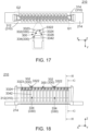
Fig. 17 is a top view showing a movable housing which is included in the connector ofFig. 9 . -
Fig. 18 is a front view showing the movable housing ofFig. 17 . -
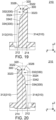
Fig. 19 is a cross-sectional view showing the movable housing ofFig. 18 , taken along line G-G. -
Fig. 20 is another cross-sectional view showing the movable housing ofFig. 18 , taken along line H-H. -
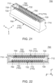
Fig. 21 is a lower, perspective view showing the mating connector which is included in the assembly ofFig. 1 . -
Fig. 22 is a bottom view showing the mating connector ofFig. 21 . -
Fig. 23 is a front view showing the mating connector ofFig. 21 . -
Fig. 24 is a cross-sectional view showing the mating connector ofFig. 23 , taken along line I-I. -
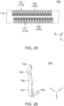
Fig. 25 is a top view showing the mating connector ofFig. 21 . -
Fig. 26 is a perspective view showing a mating contact of a first mating contact row which is included in the mating connector ofFig. 21 . -
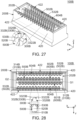
Fig. 27 is a perspective view showing a connector which is included in an assembly according to a second embodiment of the present invention. -
Fig. 28 is a top view showing the connector ofFig. 27 . -
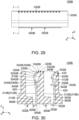
Fig. 29 is a front view showing the connector ofFig. 27 . -
Fig. 30 is a cross-sectional view showing the connector ofFig. 29 , taken along line J-J. -
Fig. 31 is a bottom view showing the connector ofFig. 27 . -
Fig. 32 is a perspective view showing a first contact of a first contact row which is included in the connector ofFig. 27 . -
Fig. 33 is a perspective view showing a second contact of a second row which is included in the connector ofFig. 27 . -
Fig. 34 is a perspective view showing a connector of Patent Document 1. In the figure, a part of the connector is enlarged and illustrated. - While the invention is susceptible to various modifications and alternative forms, specific embodiments thereof are shown by way of example in the drawings and will herein be described in detail. It should be understood, however, that the drawings and detailed description thereto are not intended to limit the invention to the particular form disclosed, but on the contrary, the intention is to cover all modifications, equivalents and alternatives falling within the spirit and scope of the present invention as defined by the appended claims.
- As shown in
Fig. 1 , anassembly 10 according to a first embodiment of the present invention comprises aconnector 100 and amating connector 700. - As shown in
Fig. 6 , themating connector 700 of the present embodiment is mateable with theconnector 100 along a mating direction. Referring toFig. 21 , themating connector 700 of the present embodiment is a plug connector. In the present embodiment, the mating direction is a Z-direction. Additionally, the mating direction is also referred to as an up-down direction. Specifically, it is assumed that upward is a positive Z-direction while downward is a negative Z-direction. - As shown in
Fig. 24 , themating connector 700 of the present embodiment comprises amating insulator 710 and a plurality ofmating contacts 750. - Referring to
Fig. 24 , themating insulator 710 of the present embodiment is made of insulator. Themating insulator 710 holds themating contacts 750. Themating insulator 710 has twoouter walls 720. - As shown in
Fig. 22 , each of theouter walls 720 of the present embodiment extends in a pitch direction. Each of theouter walls 720 has a flat-plate shape perpendicular to a width direction. The twoouter walls 720 define opposite ends, respectively, of themating insulator 710 in the width direction. Each of theouter walls 720 is formed with a plurality ofmating receiving portions 722. In the present embodiment, the pitch direction is an X-direction. Additionally, in the present embodiment, the width direction is a Y-direction. The width direction is also referred to as a front-rear direction. Specifically, it is assumed that forward is a positive Y-direction while rearward is a negative Y-direction. - As shown in
Fig. 24 , each of themating receiving portions 722 of the present embodiment pierces theouter wall 720 in the width direction. Each of themating receiving portions 722 is positioned at a lower end of themating insulator 710 in the up-down direction. - As shown in
Fig. 24 , themating insulator 710 has a partitionportion accommodating portion 712. - As shown in
Fig. 24 , the partitionportion accommodating portion 712 of the present embodiment is a space extending in the mating direction, or in the up-down direction. The partitionportion accommodating portion 712 is opened downward in the up-down direction. - Referring to
Fig. 26 , each of themating contacts 750 of the present embodiment is made of metal. Each of themating contacts 750 is a spring contact. As shown inFig. 22 , themating contacts 750 form a plurality ofmating contact rows 770. Specifically, themating contacts 750 form two of themating contact rows 770. Hereinafter, one of the twomating contact rows 770, which is positioned at a front of themating connector 700, is referred to as a firstmating contact row 771, while the othermating contact row 770 positioned at a rear of themating connector 700 is referred to as a secondmating contact row 772. Themating contact 750 of the firstmating contact row 771 and themating contact 750 of the secondmating contact row 772 have the same shape as each other. However, the present invention is not limited thereto. Specifically, themating contacts 750 may form three or more of themating contact rows 770. Themating contacts 750 correspond to themating receiving portions 722, respectively. - As shown in
Fig. 26 , each of themating contacts 750 has a matingdistal end portion 752. As shown inFigs. 6 and7 , each of themating receiving portions 722 is able to receive the matingdistal end portion 752 of thecorresponding mating contact 750 upon the mating of theconnector 100 with themating connector 700. However, the present invention is not limited thereto. Themating connector 700 should be configured as follows: themating contact rows 770 include an outermost contact row which is positioned outermost of themating contact rows 770 in the width direction; and themating receiving portion 722 is able to receive the matingdistal end portion 752 of themating contact 750 of the outermost contact row upon the mating of theconnector 100 with themating connector 700. - As shown in
Fig. 26 , each of themating contacts 750 has amating contact point 754, amating supporting portion 756, a mating heldportion 757 and a mating fixedportion 758. - As shown in
Fig. 24 , themating contact point 754 of the present embodiment faces inward in the width direction. Themating contact point 754 is positioned above the matingdistal end portion 752 in the up-down direction. - As shown in
Fig. 24 , themating supporting portion 756 of the present embodiment is positioned above themating contact point 754 in the up-down direction. Themating supporting portion 756 extends downward in the up-down direction from the mating heldportion 757. Themating supporting portion 756 is resiliently deformable. Themating contact point 754 is supported by themating supporting portion 756. In other words, themating supporting portion 756 resiliently supports themating contact point 754. Accordingly, themating contact point 754 is movable in the width direction. - Referring to
Fig. 24 , the mating fixedportion 758 of the present embodiment is fixed on a circuit board (not shown) by soldering or the like when themating connector 700 is mounted on the circuit board. The mating fixedportion 758 extends outward in the width direction from the mating heldportion 757. The mating fixedportion 758 defines an upper end of themating contact 750 in the up-down direction. The mating fixedportion 758 defines an outer end of themating contact 750 in the width direction. - As shown in
Fig. 6 , theconnector 100 of the present embodiment is mateable along the mating direction with themating connector 700 which has themating contacts 750. Theconnector 100 of the present embodiment is a receptacle connector with a floating structure. However, the present invention is not limited thereto. Specifically, theconnector 100 may be a normal receptacle connector with no floating structure, or may be a plug connector. - As shown in
Fig. 8 , theconnector 100 comprises aninsulator 200 and a plurality ofcontacts 500. - Referring to
Fig. 11 , theinsulator 200 of the present embodiment is made of insulator. Theinsulator 200 holds thecontacts 500. Theinsulator 200 has amovable housing 210, a fixedhousing 250 and anaccommodating portion 202. - As shown in
Fig. 11 , themovable housing 210 of the present embodiment has apartition portion 300. In other words, theinsulator 200 has thepartition portion 300. - As shown in
Fig. 17 , thepartition portion 300 of the present embodiment has opposite faces 310 in the width direction. The opposite faces 310 include afront face 312 and arear face 314. Thefront face 312 is positioned forward of therear face 314 in the front-rear direction. Thefront face 312 is directed forward in the front-rear direction. Therear face 314 is directed rearward in the front-rear direction. Thepartition portion 300 is formed with a plurality ofaccommodating ditches 330. - As shown in
Fig. 11 , each of theaccommodating ditches 330 of the present embodiment is recessed inward in the width direction. Each of theaccommodating ditches 330 is opened upward in the up-down direction. Each of theaccommodating ditches 330 is opened outward in the width direction. Each of theaccommodating ditches 330 communicates with theaccommodating portion 202 in the width direction. As shown inFig. 17 , theaccommodating ditches 330 are arranged in a staggered configuration. Theaccommodating ditches 330 are classified into two groups G1, G2. In the present embodiment, the number of theaccommodating ditches 330 of the group G1 is equal to the number of theaccommodating ditches 330 of the group G2. Theaccommodating ditches 330 of each of the groups G1, G2 are arranged in the pitch direction perpendicular to the mating direction. - As shown in
Fig. 17 , theaccommodating ditches 330 of one of the groups G1, G2 correspond to theaccommodating ditches 330, respectively, of a remaining one of the groups G1, G2. Theaccommodating ditches 330 of one of the groups G1, G2 are positioned on one of the opposite faces 310 of thepartition portion 300. Theaccommodating ditches 330 of a remaining one of the groups G1, G2 are positioned on a remaining one of the opposite faces 310 of thepartition portion 300. Theaccommodating ditches 330 of one of the groups G1, G2 are different in position from theaccommodating ditches 330 of a remaining one of the groups G1, G2 in the pitch direction. Each of theaccommodating ditches 330 of one of the groups G1, G2 occupies a first area in the pitch direction. Each of theaccommodating ditches 330 of a remining one of the groups G1, G2 occupies a second area in the pitch direction. The first area of each of theaccommodating ditches 330 of the one of the groups G1, G2 overlaps with the second area of one of theaccommodating ditches 330 of the remining one of the groups G1, G2 in the pitch direction. More specifically, the first area of each of theaccommodating ditches 330 of the one of the groups G1, G2 overlaps with the second area of the correspondingaccommodating ditch 330 of the remining one of the groups G1, G2 in the pitch direction. - As shown in
Fig. 17 , theaccommodating ditches 330 of the group G1 correspond to theaccommodating ditches 330, respectively, of the group G2. Theaccommodating ditches 330 of the group G1 are positioned on thefront face 312 of thepartition portion 300. Theaccommodating ditches 330 of the group G2 are positioned on therear face 314 of thepartition portion 300. Theaccommodating ditches 330 of the group G1 are different in position from theaccommodating ditches 330 of the group G2 in the pitch direction. Each of theaccommodating ditches 330 of the group G1 occupies an area in the pitch direction. Each of theaccommodating ditches 330 of the group G2 occupies another area in the pitch direction. The area of each of theaccommodating ditches 330 of the group G1 overlaps with the area of one of theaccommodating ditches 330 of the group G2 in the pitch direction. More specifically, the area of each of theaccommodating ditches 330 of the group G1 overlaps with the area of the correspondingaccommodating ditch 330 of the group G2 in the pitch direction. - As shown in
Fig. 17 , each of theaccommodating ditches 330 has a receivingportion 332. - As shown in
Figs. 19 and 20 , the receivingportion 332 of the present embodiment defines an upper end of theaccommodating ditch 330 in the up-down direction. The receivingportion 332 is opened upward in the up-down direction. The receivingportion 332 is recessed inward in the width direction. The receivingportion 332 is opened outward in the width direction. - As shown in
Figs. 19 and 20 , in the width direction, the receivingportion 332 extends across a middle 320 of thepartition portion 300. - As described above, the
accommodating ditches 330 of the one of the groups G1, G2 are different in position from theaccommodating ditches 330 of the remaining one of the groups G1, G2 in the pitch direction, and the receivingportion 332 extends across the middle 320 of thepartition portion 300 in the width direction. This enables thepartition portion 300 of theconnector 100 of the present embodiment to have a reduced thickness in the width direction. Specifically, theconnector 100 of the present embodiment can have a reduced size in the width direction. - More specifically, referring to
Figs. 17 and19 , the receivingportion 332 of each of theaccommodating ditches 330 of the group G1, which is positioned on thefront face 312 of thepartition portion 300, extends across the middle 320 of thepartition portion 300 toward therear face 314 of thepartition portion 300. It is noted that the receivingportion 332 of each of theaccommodating ditches 330 of the group G1 does not reach therear face 314 of thepartition portion 300. - Additionally, referring to
Figs. 17 and20 , the receivingportion 332 of each of theaccommodating ditches 330 of the group G2, which is positioned on therear face 314 of thepartition portion 300, extends across the middle 320 of thepartition portion 300 toward thefront face 312 of thepartition portion 300. It is noted that the receivingportion 332 of each of theaccommodating ditches 330 of the group G2 does not reach thefront face 312 of thepartition portion 300. - As shown in
Fig. 17 , the receivingportion 332 has anarrow portion 3322 and awide portion 3326. - As shown in
Fig. 17 , thenarrow portion 3322 of the present embodiment is positioned inward of thewide portion 3326 in the width direction. Thenarrow portion 3322 defines an inner end of the receivingportion 332 in the width direction. Thenarrow portion 3322 communicates with thewide portion 3326 in the width direction. Thenarrow portion 3322 has aninner surface 3323. In other words, each of the receivingportions 332 does not pierce thepartition portion 300 in the width direction. - As described above, the
insulator 200 of the present embodiment is configured so that each of the receivingportions 332 does not pierce thepartition portion 300 in the width direction. Accordingly, molten resin can easily flow when theinsulator 200 of the present embodiment is molded. However, the present invention is not limited thereto, but the receivingportion 332 may pierce thepartition portion 300 in the width direction. - As shown in
Figs. 19 and 20 , theinner surface 3323 defines an inner end of thenarrow portion 3322 in the width direction. Theinner surface 3323 faces outward in the width direction. Theinner surface 3323 is a plane perpendicular to the width direction. Referring toFigs. 17 and19 , theinner surface 3323 of the receivingportion 332 of each of theaccommodating ditches 330 of the group G1 is positioned rearward of the middle 320 of thepartition portion 300 in the front-rear direction. Referring toFigs. 17 and20 , theinner surface 3323 of the receivingportion 332 of each of theaccommodating ditches 330 of the group G2 is positioned forward of the middle 320 of thepartition portion 300 in the front-rear direction. - As shown in
Fig. 17 , thewide portion 3326 of the present embodiment is positioned outward of thenarrow portion 3322 in the width direction. Thewide portion 3326 defines an outer end of the receivingportion 332 in the width direction. A size of a part of thewide portion 3326 in the pitch direction decreases as the part approaches thenarrow portion 3322. As shown inFig. 19 , thewide portion 3326 couples thenarrow portion 3322 and anadditional receiving portion 334 with each other. - As shown in
Fig. 19 , the receivingportion 332 has afirst surface 3324 facing in the mating direction. Thefirst surface 3324 is oblique to both the mating direction and the width direction. Thefirst surface 3324 faces upward in the up-down direction and outward in the width direction. Thefirst surface 3324 extends upward in the up-down direction and inward in the width direction. - As shown in
Fig. 19 , each of theaccommodating ditches 330 further has the additional receivingportion 334. - As shown in
Fig. 19 , the additional receivingportion 334 of the present embodiment is positioned below the receivingportion 332 in the up-down direction. Referring toFigs. 6 and11 , the additional receivingportion 334 partially receives a supportingportion 540 upon the mating of theconnector 100 with themating connector 700. As shown inFig. 19 , the additional receivingportion 334 has asecond surface 3342 facing in the mating direction. Thesecond surface 3342 is oblique to both the mating direction and the width direction. Thesecond surface 3342 faces upward in the up-down direction and outward in the width direction. Thesecond surface 3342 extends upward in the up-down direction and inward in the width direction. A first angle that thefirst surface 3324 makes with the mating direction is greater than a second angle that thesecond surface 3342 makes with the mating direction. An angle that thefirst surface 3324 makes with the width direction is smaller than an angle that thesecond surface 3342 makes with the width direction. - As shown in
Figs.19 and 20 , themovable housing 210 has a plurality of first holdingportions 212. Each of the first holdingportions 212 is positioned around a lower end of themovable housing 210 in the up-down direction. Each of the first holdingportions 212 is positioned below thepartition portion 300 in the up-down direction. - As shown in
Fig. 19 , themovable housing 210 has abase portion 214. Thebase portion 214 defines the lower end of themovable housing 210 in the up-down direction. Thepartition portion 300 extends upward in the up-down direction from thebase portion 214. - As shown in
Fig. 9 , the fixedhousing 250 defines an outer end of theinsulator 200 in a direction perpendicular to the mating direction. The fixedhousing 250 defines opposite outer ends of theinsulator 200 in the width direction perpendicular to the mating direction. The fixedhousing 250 defines opposite outer ends of theinsulator 200 in the pitch direction perpendicular to both the mating direction and the width direction. Thepartition portion 300 is surrounded by the fixedhousing 250 in a plane perpendicular to the up-down direction. - As shown in
Figs. 11 and 12 , the fixedhousing 250 has a plurality of second holdingportions 252. Each of thesecond holding portions 252 is positioned around a lower end of the fixedhousing 250 in the up-down direction. Each of thesecond holding portions 252 is positioned around an outer end of the fixedhousing 250 in the width direction. - As shown in
Fig. 9 , theaccommodating portion 202 of the present embodiment is opened upward in the up-down direction. Theaccommodating portion 202 is surrounded by the fixedhousing 250 in the plane perpendicular to the up-down direction. As shown inFig. 6 , theaccommodating portion 202 accommodates a part of themating connector 700 when theconnector 100 and themating connector 700 are mated with each other. - Referring to
Fig. 15 , each of thecontacts 500 of the present embodiment is made of metal. Each of thecontacts 500 is a spring contact. As shown inFig. 6 , thecontact 500 is brought into contact with themating contact 750 at two points when theconnector 100 and themating contact 750 are mated with each other. Themating contact point 754 is brought into contact with thecontact 500 upon the mating of theconnector 100 with themating connector 700. As shown inFig. 9 , thecontacts 500 are arranged in a staggered configuration. Thecontacts 500 from twocontact rows 600. Hereinafter, one of thecontact rows 600, which is positioned at a front of theconnector 100, is referred to as afirst contact row 601, while theother contact row 600 positioned at a rear of theconnector 100 is referred to as asecond contact row 602. Thecontact 500 of thefirst contact row 601 and thecontact 500 of thesecond contact row 602 have the same shape as each other. - As shown in
Fig. 9 , thecontacts 500 correspond to theaccommodating ditches 330, respectively. Each of thecontacts 500 is partially accommodated in the correspondingaccommodating ditch 330. - Referring to
Figs. 9 and17 , thecontacts 500 of thefirst contact row 601 correspond to theaccommodating ditches 330, respectively, of the group G1. Thecontacts 500 of thesecond contact row 602 correspond to theaccommodating ditches 330, respectively, of the group G2. Each of thecontacts 500 of thefirst contact row 601 is partially accommodated in the correspondingaccommodating ditch 330 of the group G1. Each of thecontacts 500 of thesecond contact row 602 is partially accommodated in the correspondingaccommodating ditch 330 of the group G2. - As shown in
Fig. 15 , each of thecontacts 500 has acontact point 510 and adistal end portion 530. - As shown in
Fig. 9 , thecontact point 510 of the present embodiment faces outward in the width direction. Thecontact point 510 is positioned in theaccommodating portion 202. Thenarrow portion 3322 of the receivingportion 332 of each of theaccommodating ditches 330 is smaller than thecontact point 510 of thecorresponding contact 500. That is, in the pitch direction, a size of thenarrow portion 3322 of the receivingportion 332 of each of theaccommodating ditches 330 is smaller than a size of thecontact point 510 of thecorresponding contact 500. As shown inFig. 6 , thecontact point 510 is brought into contact with themating contact 750 when theconnector 100 and themating connector 700 are mated with each other. - As shown in
Fig. 15 , thedistal end portion 530 of the present embodiment defines a free end of thecontact 500. Thedistal end portion 530 is positioned at an upper end of thecontact 500 in the up-down direction. In each of thecontacts 500, thedistal end portion 530 is smaller than thecontact point 510. More specifically, in each of thecontacts 500, the whole part of thedistal end portion 530 is smaller than thecontact point 510. That is, in the pitch direction, a size of thedistal end portion 530 is smaller than the size of thecontact point 510. - As shown in
Fig. 6 , the receivingportion 332 of each of theaccommodating ditches 330 is able to receive thedistal end portion 530 of thecorresponding contact 500 upon the mating of theconnector 100 with themating connector 700. However, the present invention is not limited thereto. Specifically, the receivingportion 332 of each of theaccommodating ditches 330 should be able to receive, at least in part, thedistal end portion 530 of thecorresponding contact 500 upon the mating of theconnector 100 with themating connector 700. Thenarrow portion 3322 of the receivingportion 332 of each of theaccommodating ditches 330 receives a part of thedistal end portion 530 of thecorresponding contact 500 upon the mating of theconnector 100 with themating connector 700. It is noted that theinner surface 3323 of thenarrow portion 3322 of the receivingportion 332 of each of theaccommodating ditches 330 is in non-contact with thedistal end portion 530 of thecorresponding contact 500 upon the mating of theconnector 100 with themating connector 700. - As shown in
Fig. 15 , each of thecontacts 500 further has aguide portion 520. - As shown in
Fig. 11 , theguide portion 520 of the present embodiment extends upward in the up-down direction and inward in the width direction from thecontact point 510. Theguide portion 520 extends downward in the up-down direction and outward in the width direction from thedistal end portion 530. Theguide portion 520 couples thecontact point 510 and thedistal end portion 530 with each other. Theguide portion 520 intersects with the mating direction, or with the up-down direction. As shown inFig. 15 , in each of thecontacts 500, thedistal end portion 530 is smaller than theguide portion 520. That is, in the pitch direction, the size of thedistal end portion 530 is smaller than a size of theguide portion 520. Theguide portion 520 has amain portion 5202 and a taperedportion 5204. - As shown in
Fig. 15 , themain portion 5202 of the present embodiment defines an outer end of theguide portion 520 in the width direction. Themain portion 5202 couples thecontact point 510 and the taperedportion 5204 with each other. Themain portion 5202 has a constant size in the pitch direction. In the pitch direction, the size of themain portion 5202 is greater than the size of thedistal end portion 530. - As shown in
Fig. 15 , the taperedportion 5204 of the present embodiment defines an inner end of theguide portion 520 in the width direction. The taperedportion 5204 is coupled with thedistal end portion 530. The taperedportion 5204 is tapered toward thedistal end portion 530. - As shown in
Fig. 15 , each of thecontacts 500 further has the supportingportion 540. - As shown in
Fig. 15 , the supportingportion 540 of the present embodiment is positioned below thecontact point 510 in the up-down direction. The supportingportion 540 is resiliently deformable. Thecontact point 510 is supported by the supportingportion 540. In other words, the supportingportion 540 resiliently supports thecontact point 510. Accordingly, thecontact point 510 is movable in the width direction. - As shown in
Fig. 15 , each of thecontacts 500 further has a fixedportion 550, a first heldportion 560, aconnection portion 570 and a second heldportion 580. - Referring to
Figs. 11 and15 , the fixedportion 550 of the present embodiment is fixed on a circuit board (not shown) by soldering or the like when theconnector 100 is mounted on the circuit board. The fixedportion 550 extends outward in the width direction. The fixedportion 550 defines an outer end of thecontact 500 in the width direction. The fixedportion 550 defines a lower end of thecontact 500 in the up-down direction. - As shown in
Fig. 15 , the first heldportion 560 of the present embodiment extends upward in the up-down direction from theconnection portion 570. As shown inFig. 11 , the first heldportion 560 is held by thefirst holding portion 212. More specifically, the first heldportion 560 is press-fit into thefirst holding portion 212. - As shown in
Fig. 15 , theconnection portion 570 of the present embodiment couples the first heldportion 560 and the second heldportion 580 with each other. Theconnection portion 570 is resiliently deformable. Referring toFig. 11 , themovable housing 210 is movable relative to the fixedhousing 250 in the plane perpendicular to the up-down direction by the resilient deformations of theconnection portions 570. - As shown in
Fig. 15 , the second heldportion 580 of the present embodiment extends upward in the up-down direction from the fixedportion 550. The second heldportion 580 extends downward in the up-down direction from theconnection portion 570. As shown inFig. 11 , the second heldportion 580 is held by thesecond holding portion 252. More specifically, the second heldportion 580 is press-fit into thesecond holding portion 252. - The structure of the
contact 500 is not limited thereto. For example, thecontact 500 can be modified as described below. - As shown in
Fig. 16 , acontact 500A according to a modification of the present invention has acontact point 510, aguide portion 520A, adistal end portion 530A, a supportingportion 540, a fixedportion 550, a first heldportion 560, aconnection portion 570 and a second heldportion 580. Components of thecontact 500A other than theguide portion 520A and thedistal end portion 530A have structures same as those of the aforementioned embodiment. Accordingly, a detailed description thereabout is omitted. - As shown in
Fig. 16 , dissimilar to theguide portion 520 of thecontact 500 of the aforementioned embodiment, theguide portion 520A of the present modification consists only of amain portion 5202A which has a constant size in the pitch direction. Dissimilar to thedistal end portion 530 of thecontact 500 of the aforementioned embodiment, thedistal end portion 530A of the present modification is tapered from theguide portion 520A toward a free end of thecontact 500A. It is noted that, in anassembly 10 of the present modification, the receivingportion 332 of each of theaccommodating ditches 330 of thepartition portion 300 of theinsulator 200 is able to receive, at least in part, thedistal end portion 530A of a corresponding one of thecontacts 500A upon mating of aconnector 100 with themating connector 700. - Referring to
Fig. 27 , an assembly (not shown) according to a second embodiment of the present invention comprises aconnector 100B and a mating connector (not shown). - Referring to
Fig. 27 , theconnector 100B of the present embodiment is mateable along the mating direction with the mating connector which has mating contacts (not shown). Dissimilar to theconnector 100 and themating connector 700 of the aforementioned embodiment, theconnector 100B of the present embodiment is a plug connector while the mating connector of the present embodiment is a receptacle connector. As for directions and orientations in the present embodiment, expressions same as those of the first embodiment will be used hereinbelow. - As shown in
Fig. 27 , theconnector 100B comprises aninsulator 200B, a plurality offirst contacts 500B and a plurality ofsecond contacts 502B. Thefirst contact 500B is also referred to as acontact 500B. - Referring to
Fig. 28 , theinsulator 200B of the present embodiment is made of insulator. Theinsulator 200B defines an outer end of theconnector 100B in a direction perpendicular to the mating direction. Theinsulator 200B defines opposite outer ends of theconnector 100B in the width direction perpendicular to the mating direction. Theinsulator 200B defines opposite outer ends of theconnector 100B in the pitch direction perpendicular to both the mating direction and the width direction. Theinsulator 200B holds thecontacts 500B. - As shown in
Fig. 30 ,insulator 200B has apartition portion 300B. - As shown in
Fig. 30 , thepartition portion 300B of the present embodiment has opposite faces 310B in the width direction. The opposite faces 310B include afront face 312B and arear face 314B. Thefront face 312B is positioned forward of therear face 314B in the front-rear direction. Thefront face 312B is directed forward in the front-rear direction. Therear face 314B is directed rearward in the front-rear direction. As shown inFig. 28 , thepartition portion 300B is formed with a plurality ofaccommodating ditches 330B. - As shown in
Fig. 30 , each of theaccommodating ditches 330B of the present embodiment is recessed inward in the width direction. Each of theaccommodating ditches 330B is opened upward in the up-down direction. Each of theaccommodating ditches 330B is opened outward in the width direction. As shown inFig. 28 , theaccommodating ditches 330B are arranged in a staggered configuration. The accommodating ditches 330B are classified into two groups G1, G2. In the present embodiment, the number of theaccommodating ditches 330B of the group G1 is equal to the number of theaccommodating ditches 330B of the group G2. The accommodating ditches 330B of each of the groups G1, G2 are arranged in the pitch direction perpendicular to the mating direction. - As shown in
Fig. 28 , theaccommodating ditches 330B of one of the groups G1, G2 correspond to theaccommodating ditches 330B, respectively, of a remaining one of the groups G1, G2. The accommodating ditches 330B of one of the groups G1, G2 are positioned on one of the opposite faces 310B of thepartition portion 300B. The accommodating ditches 330B of a remaining one of the groups G1, G2 are positioned on a remaining one of the opposite faces 310B of thepartition portion 300B. The accommodating ditches 330B of one of the groups G1, G2 are different in position from theaccommodating ditches 330B of a remaining one of the groups G1, G2 in the pitch direction. Each of theaccommodating ditches 330B of one of the groups G1, G2 occupies a first area in the pitch direction. Each of theaccommodating ditches 330B of a remining one of the groups G1, G2 occupies a second area in the pitch direction. The first area of each of theaccommodating ditches 330B of the one of the groups G1, G2 overlaps with the second area of one of theaccommodating ditches 330B of the remining one of the groups G1, G2 in the pitch direction. More specifically, the first area of each of theaccommodating ditches 330B of the one of the groups G1, G2 overlaps with the second area of the correspondingaccommodating ditch 330B of the remining one of the groups G1, G2 in the pitch direction. - As shown in
Fig. 28 , theaccommodating ditches 330B of the group G1 correspond to theaccommodating ditches 330B, respectively, of the group G2. The accommodating ditches 330B of the group G1 are positioned on thefront face 312B of thepartition portion 300B. The accommodating ditches 330B of the group G2 are positioned on therear face 314B of thepartition portion 300B. The accommodating ditches 330B of the group G1 are different in position from theaccommodating ditches 330B of the group G2 in the pitch direction. Each of theaccommodating ditches 330B of the group G1 occupies an area in the pitch direction. Each of theaccommodating ditches 330B of the group G2 occupies another area in the pitch direction. The area of each of theaccommodating ditches 330B of the group G1 overlaps with the area of one of theaccommodating ditches 330B of the group G2 in the pitch direction. More specifically, the area of each of theaccommodating ditches 330B of the group G1 overlaps with the area of the correspondingaccommodating ditch 330 of the group G2 in the pitch direction. - As shown in
Fig. 30 , each of theaccommodating ditches 330B has a receivingportion 332B. - As shown in
Fig. 30 , the receivingportion 332B of the present embodiment defines an upper end of theaccommodating ditch 330B in the up-down direction. The receivingportion 332B is opened upward in the up-down direction. The receivingportion 332B is recessed inward in the width direction. The receivingportion 332B is opened outward in the width direction. In the width direction, the receivingportion 332B extends across a middle 320B of thepartition portion 300B. - As described above, the
accommodating ditches 330B of the one of the groups G1, G2 are different in position from theaccommodating ditches 330B of the remaining one of the groups G1, G2 in the pitch direction, and the receivingportion 332B extends across the middle 320B of thepartition portion 300B in the width direction. This enables thepartition portion 300B of theconnector 100B of the present embodiment to have a reduced thickness in the width direction. Specifically, theconnector 100B of the present embodiment can have a reduced size in the width direction. - As shown in
Fig. 30 , the receivingportion 332B has anarrow portion 3322B and awide portion 3326B. Thenarrow portion 3322B and thewide portion 3326B of the present embodiment have structures same as those of thenarrow portion 3322 and thewide portion 3326 of the aforementioned embodiment. Accordingly, a detailed description thereabout is omitted. - As shown in
Fig. 30 , each of theaccommodating ditches 330B further has an additional receiving portion 334B. The additional receiving portion 334B of the present embodiment has a structure same as that of the additional receivingportion 334 of the aforementioned embodiment. Accordingly, a detailed description thereabout is omitted. - As shown in
Fig. 30 , theinsulator 200B has a plurality of first holdingportions 212B, twoouter walls 420 and anaccommodating portion 202B. - As shown in
Fig. 30 , each of the first holdingportions 212B of the present embodiment is positioned around a lower end of theinsulator 200B in the up-down direction. Each of the first holdingportions 212B is positioned below thepartition portion 300B in the up-down direction. - As shown in
Fig. 28 , each of theouter walls 420 of the present embodiment extends in the pitch direction. Each of theouter walls 420 has a flat-plate shape perpendicular to the width direction. The twoouter walls 420 define opposite ends, respectively, of theinsulator 200B in the width direction. Thepartition portion 300B is positioned between the twoouter walls 420 in the width direction. Each of theouter walls 420 is formed with a plurality of outer wall-side receiving portions 422. - As shown in
Fig. 30 , each of the outer wall-side receiving portions 422 of the present embodiment pierces theouter wall 420 in the width direction. Each of the outer wall-side receiving portions 422 is positioned at an upper end of theinsulator 200B in the up-down direction. - As shown in
Fig. 30 , each of theouter walls 420 has a plurality of second holdingportions 252B. - As shown in
Fig. 30 , each of thesecond holding portions 252B of the present embodiment is positioned around a lower end of theouter wall 420 in the up-down direction. Each of thesecond holding portions 252B is positioned outward of thepartition portion 300B in the width direction. - As shown in
Fig. 30 , theaccommodating portion 202B of the present embodiment is opened upward in the up-down direction. Each of theaccommodating ditches 330B communicates with theaccommodating portion 202B in the width direction. Referring toFig. 30 , theaccommodating portion 202B accommodates a part of the mating connector when theconnector 100B and the mating connector are mated with each other. - Referring to
Fig. 32 , each of thefirst contacts 500B of the present embodiment is made of metal. Each of thefirst contacts 500B is a spring contact. Referring toFig. 30 , thefirst contact 500B is brought into contact with the mating contact when theconnector 100B and the mating connector are mated with each other. As shown inFig. 28 , thefirst contacts 500B are arranged in a staggered configuration. Thefirst contacts 500B from twocontact rows 600B. Hereinafter, one of thecontact rows 600B, which is positioned at a front of theconnector 100B, is referred to as afirst contact row 601B, while theother contact row 600B positioned at a rear of theconnector 100B is referred to as asecond contact row 602B. Thefirst contact 500B of thefirst contact row 601B and thefirst contact 500B of thesecond contact row 602B have the same shape as each other. - As shown in
Fig. 30 , thefirst contacts 500B correspond to theaccommodating ditches 330B, respectively. Each of thefirst contacts 500B is partially accommodated in the correspondingaccommodating ditch 330B. - As shown in
Fig. 28 , thefirst contacts 500B of thefirst contact row 601B correspond to theaccommodating ditches 330B, respectively, of the group G1. Thefirst contacts 500B of thesecond contact row 602B correspond to theaccommodating ditches 330B, respectively, of the group G2. Each of thefirst contacts 500B of thefirst contact row 601B is partially accommodated in the correspondingaccommodating ditch 330B of the group G1. Each of thefirst contacts 500B of thesecond contact row 602B is partially accommodated in the correspondingaccommodating ditch 330B of the group G2. - As shown in
Fig. 32 , each of thefirst contacts 500B has acontact point 510B and adistal end portion 530B. Thecontact point 510B and thedistal end portion 530B of the present embodiment have structures same as those of thecontact point 510 and thedistal end portion 530 of the aforementioned embodiment. Accordingly, a detailed description thereabout is omitted. - As shown in
Fig. 32 , each of thefirst contacts 500B further has aguide portion 520B. Theguide portion 520B has amain portion 5202B and a taperedportion 5204B. Themain portion 5202B and the taperedportion 5204B of the present embodiment have structures same as those of themain portion 5202 and the taperedportion 5204 of the aforementioned embodiment. Accordingly, a detailed description thereabout is omitted. - As shown in
Fig. 32 , each of thefirst contacts 500B further has a supportingportion 540B. The supportingportion 540B of the present embodiment has a structure same as that of the supportingportion 540 of the aforementioned embodiment. Accordingly, a detailed description thereabout is omitted. - As shown in
Fig. 32 , each of thefirst contacts 500B further has a fixedportion 550B and a heldportion 560B. - Referring to
Fig. 30 , the fixedportion 550B of the present embodiment is fixed on a circuit board (not shown) by soldering or the like when theconnector 100B is mounted on the circuit board. The fixedportion 550B extends outward in the width direction. - As shown in
Fig. 32 , the heldportion 560B of the present embodiment extends upward in the up-down direction from the fixedportion 550B. The heldportion 560B extends downward in the up-down direction from the supportingportion 540B. The heldportion 560B couples the fixedportion 550B and the supportingportion 540B with each other. As shown inFig. 30 , the heldportion 560B is held by thefirst holding portion 212B. More specifically, the heldportion 560B is press-fit into thefirst holding portion 212B. - Referring to
Fig. 33 , each of thesecond contacts 502B of the present embodiment is made of metal. Each of thesecond contacts 502B is a spring contact. Referring toFig. 30 , thesecond contact 502B is brought into contact with the mating contact when theconnector 100B and the mating connector are mated with each other. As shown inFig. 28 , thesecond contacts 502B from twocontact rows 604B. Hereinafter, one of thecontact rows 604B, which is positioned at the front of theconnector 100B, is referred to as a first row, while theother contact row 604B positioned at the rear of theconnector 100B is referred to as a second row. Thesecond contact 502B of the first row and thesecond contact 502B of the second row have the same shape as each other. Thesecond contacts 502B correspond to the outer wall-side receiving portions 422, respectively. - As shown in
Fig. 33 , each of thesecond contacts 502B has acontact point 512B and adistal end portion 532B. - As shown in
Fig. 30 , thecontact point 512B of the present embodiment faces inward in the width direction. Thecontact point 512B is positioned in theaccommodating portion 202B. Thecontact point 512B is brought into contact with the mating contact when theconnector 100B and the mating connector are mated with each other. - As shown in
Fig. 33 , thedistal end portion 532B of the present embodiment defines a free end of thesecond contact 502B. Thedistal end portion 532B is positioned at an upper end of thesecond contact 502B in the up-down direction. In each of thesecond contacts 502B, thedistal end portion 532B is smaller than thecontact point 512B. More specifically, in each of thesecond contacts 502B, the whole part of thedistal end portion 532B is smaller than thecontact point 512B. That is, in the pitch direction, a size of thedistal end portion 532B is smaller than a size of thecontact point 512B. Referring toFig. 30 , the outer wall-side receiving portion 422 is able to receive thedistal end portion 532B of the correspondingsecond contact 502B upon the mating of theconnector 100B with the mating connector. - As shown in
Fig. 33 , each of thesecond contacts 502B further has aguide portion 522B. - As shown in
Fig. 30 , theguide portion 522B of the present embodiment extends upward in the up-down direction and outward in the width direction from thecontact point 512B. Theguide portion 522B extends downward in the up-down direction and inward in the width direction from thedistal end portion 532B. Theguide portion 522B couples thecontact point 512B and thedistal end portion 532B with each other. Theguide portion 522B intersects with the mating direction, or with the up-down direction. As shown inFig. 33 , in each of thesecond contacts 502B, thedistal end portion 532B is smaller than theguide portion 522B. That is, in the pitch direction, the size of thedistal end portion 532B is smaller than a size of theguide portion 522B. Theguide portion 522B has amain portion 5222B and a taperedportion 5224B. - As shown in
Fig. 33 , themain portion 5222B of the present embodiment defines an inner end of theguide portion 522B in the width direction. Themain portion 5222B couples thecontact point 512B and the taperedportion 5224B with each other. Themain portion 5222B has a constant size in the pitch direction. In the pitch direction, a size of themain portion 5222B is greater than the size of thedistal end portion 532B. - As shown in
Fig. 33 , the taperedportion 5224B of the present embodiment defines an outer end of theguide portion 522B in the width direction. The taperedportion 5224B is coupled with thedistal end portion 532B. The taperedportion 5224B is tapered toward thedistal end portion 532B. - As shown in
Fig. 33 , each of thesecond contacts 502B further has a supportingportion 542B. - As shown in
Fig. 33 , the supportingportion 542B of the present embodiment is positioned below thecontact point 512B in the up-down direction. The supportingportion 542B is resiliently deformable. Thecontact point 512B is supported by the supportingportion 542B. That is, the supportingportion 542B resiliently supports thecontact point 512B. Accordingly, thecontact point 512B is movable in the width direction. - As shown in
Fig. 33 , each of thesecond contacts 502B further has a fixedportion 552B and a heldportion 562B. - Referring to
Fig. 30 , the fixedportion 552B of the present embodiment is fixed on the circuit board (not shown) by soldering or the like when theconnector 100B is mounted on the circuit board. The fixedportion 552B extends inward in the width direction. - As shown in
Fig. 33 , the heldportion 562B of the present embodiment extends upward in the up-down direction from the fixedportion 552B. The heldportion 562B extends downward in the up-down direction from the supportingportion 542B. The heldportion 562B couples the fixedportion 552B and the supportingportion 542B with each other. As shown inFig. 30 , the heldportion 562B is held by thesecond holding portion 252B. More specifically, the heldportion 562B is press-fit into thesecond holding portion 252B. - Although the preceding description explains the embodiments of the present invention with reference to the drawings in which the assembly, the connectors and the mating connector have the specific shapes, the present invention is not limited thereto. Specifically, the
assembly 10 and theconnector - Although the
connector 100 of the first embodiment has the twocontact rows 600, the present invention is not limited thereto. Specifically, theconnector 100 may have three or more of thecontact rows 600. - Although the
connector 100B of the second embodiment has the fourcontact rows connector 100B may have five or more of thecontact rows - While there has been described what is believed to be the preferred embodiment of the invention, those skilled in the art will recognize that other and further modifications may be made thereto without departing from the spirit of the invention, and it is intended to claim all such embodiments that fall within the true scope of the invention.
Claims (6)
- A connector mateable along a mating direction with a mating connector which has a mating contact, wherein:the connector has an insulator and a plurality of contacts;the insulator holds the contacts;the insulator has a partition portion;the partition portion has opposite faces in a width direction perpendicular to the mating direction;the partition portion is formed with a plurality of accommodating ditches;the accommodating ditches are classified into two groups;the accommodating ditches of each of the groups are arranged in a pitch direction perpendicular to both the mating direction and the width direction;the accommodating ditches of one of the groups are positioned on one of the opposite faces of the partition portion;the accommodating ditches of a remaining one of the groups are positioned on a remaining one of the opposite faces of the partition portion;the accommodating ditches of one of the groups are different in position from the accommodating ditches of a remaining one of the groups in the pitch direction;each of the accommodating ditches has a receiving portion;in the width direction, the receiving portion extends across a middle of the partition portion;the contacts correspond to the accommodating ditches, respectively;each of the contacts is partially accommodated in the corresponding accommodating ditch;the contacts form two contact rows;each of the contacts has a contact point and a distal end portion;the contact point is brought into contact with the mating contact when the connector and the mating connector are mated with each other; andthe receiving portion of each of the accommodating ditches is able to receive, at least in part, the distal end portion of the corresponding contact upon the mating of the connector with the mating connector.
- The connector as recited in claim 1, wherein:in each of the contacts, the distal end portion is smaller than the contact point;the receiving portion has a narrow portion;the narrow portion of the receiving portion of each of the accommodating ditches is smaller than the contact point of the corresponding contact;each of the accommodating ditches of one of the groups occupies a first area in the pitch direction;each of the accommodating ditches of a remining one of the groups occupies a second area in the pitch direction; andthe first area of each of the accommodating ditches of the one of the groups overlaps with the second area of one of the accommodating ditches of the remining one of the groups in the pitch direction.
- The connector as recited in claim 1 or 2, wherein:each of the contacts further has a guide portion;the guide portion couples the contact point and the distal end portion with each other; andthe guide portion intersects with the mating direction.
- The connector as recited in one of claims 1 to 3, wherein:each of the contacts further has a supporting portion;the supporting portion resiliently supports the contact point;each of the accommodating ditches further has an additional receiving portion; andthe additional receiving portion partially receives the supporting portion upon the mating of the connector with the mating connector.
- The connector as recited in claim 4, wherein:the receiving portion has a first surface facing in the mating direction;the additional receiving portion has a second surface facing in the mating direction;the first surface and the mating direction make a first angle;the second surface and the mating direction make a second angle; andthe first angle is greater than the second angle.
- An assembly comprising the connector as recited in one of claims 1 to 5 and the mating connector, wherein:the mating connector comprises a mating insulator and a plurality of the mating contacts;the mating insulator holds the mating contacts;the mating insulator has two outer walls;each of the outer walls extends in the pitch direction;each of the outer walls is formed with a plurality of mating receiving portions;each of the mating receiving portions pierces the outer wall in the width direction;the mating contacts form mating contact rows;the mating contact rows include an outermost contact row which is positioned outermost of the mating contact rows in the width direction;each of the mating contacts has a mating distal end portion; andthe mating receiving portion is able to receive the mating distal end portion of the mating contact of the outermost contact row upon the mating of the connector with the mating connector.
Applications Claiming Priority (1)
| Application Number | Priority Date | Filing Date | Title |
|---|---|---|---|
| JP2023175418A JP2025065897A (en) | 2023-10-10 | 2023-10-10 | Connectors and Assemblies |
Publications (2)
| Publication Number | Publication Date |
|---|---|
| EP4539257A1 true EP4539257A1 (en) | 2025-04-16 |
| EP4539257B1 EP4539257B1 (en) | 2026-03-25 |
Family
ID=92593150
Family Applications (1)
| Application Number | Title | Priority Date | Filing Date |
|---|---|---|---|
| EP24196856.9A Active EP4539257B1 (en) | 2023-10-10 | 2024-08-28 | Connector and assembly |
Country Status (4)
| Country | Link |
|---|---|
| US (1) | US20250118921A1 (en) |
| EP (1) | EP4539257B1 (en) |
| JP (1) | JP2025065897A (en) |
| CN (1) | CN119812816A (en) |
Citations (2)
| Publication number | Priority date | Publication date | Assignee | Title |
|---|---|---|---|---|
| US10312637B2 (en) * | 2017-01-11 | 2019-06-04 | Foxconn Interconnect Technology Limited | Electrical connector having seamless shielding shell and single row of contacts |
| JP7109303B2 (en) * | 2018-08-07 | 2022-07-29 | 日本航空電子工業株式会社 | connector assembly |
-
2023
- 2023-10-10 JP JP2023175418A patent/JP2025065897A/en active Pending
-
2024
- 2024-08-23 US US18/813,301 patent/US20250118921A1/en active Pending
- 2024-08-28 EP EP24196856.9A patent/EP4539257B1/en active Active
- 2024-09-05 CN CN202411242584.3A patent/CN119812816A/en active Pending
Patent Citations (2)
| Publication number | Priority date | Publication date | Assignee | Title |
|---|---|---|---|---|
| US10312637B2 (en) * | 2017-01-11 | 2019-06-04 | Foxconn Interconnect Technology Limited | Electrical connector having seamless shielding shell and single row of contacts |
| JP7109303B2 (en) * | 2018-08-07 | 2022-07-29 | 日本航空電子工業株式会社 | connector assembly |
Also Published As
| Publication number | Publication date |
|---|---|
| JP2025065897A (en) | 2025-04-22 |
| EP4539257B1 (en) | 2026-03-25 |
| US20250118921A1 (en) | 2025-04-10 |
| CN119812816A (en) | 2025-04-11 |
Similar Documents
| Publication | Publication Date | Title |
|---|---|---|
| EP3916925B1 (en) | Floating connector | |
| EP1391011B1 (en) | Floatable connector assembly with a staggered overlapping contact pattern | |
| US9871323B2 (en) | Electrical connector with reduced stack height | |
| EP1256145B1 (en) | Connector with shielding | |
| EP3660985A1 (en) | Connector | |
| US10601179B2 (en) | Connector | |
| US5545051A (en) | Board to board matable assembly | |
| US20210376509A1 (en) | Floating connector | |
| US12456828B2 (en) | Hybrid card edge connector | |
| US7727001B2 (en) | Electrical connector assembly | |
| US20220328994A1 (en) | Connector | |
| KR100416432B1 (en) | Electrical Connectors and Connector Assemblies | |
| US7988487B2 (en) | Connector | |
| EP4539257B1 (en) | Connector and assembly | |
| US5445529A (en) | Connector apparatus | |
| US12469996B2 (en) | Connector and connector assembly | |
| US12431649B2 (en) | Mateable surface mount connectors with different distances between contact points | |
| JP3143222U (en) | Connector with improved dual beam contact | |
| CN117039497A (en) | Electrical connectors and electrical connector components | |
| US20230067502A1 (en) | Connector | |
| EP0354064A2 (en) | Multi-pin elecrical connector of low insertion force type | |
| JPH0332062Y2 (en) | ||
| CN2261097Y (en) | Long connector | |
| JPH01235177A (en) | Method of forming and arranging contacts in electric connector | |
| JP2025021704A (en) | connector |
Legal Events
| Date | Code | Title | Description |
|---|---|---|---|
| PUAI | Public reference made under article 153(3) epc to a published international application that has entered the european phase |
Free format text: ORIGINAL CODE: 0009012 |
|
| STAA | Information on the status of an ep patent application or granted ep patent |
Free format text: STATUS: THE APPLICATION HAS BEEN PUBLISHED |
|
| AK | Designated contracting states |
Kind code of ref document: A1 Designated state(s): AL AT BE BG CH CY CZ DE DK EE ES FI FR GB GR HR HU IE IS IT LI LT LU LV MC ME MK MT NL NO PL PT RO RS SE SI SK SM TR |
|
| STAA | Information on the status of an ep patent application or granted ep patent |
Free format text: STATUS: REQUEST FOR EXAMINATION WAS MADE |
|
| 17P | Request for examination filed |
Effective date: 20250826 |
|
| GRAP | Despatch of communication of intention to grant a patent |
Free format text: ORIGINAL CODE: EPIDOSNIGR1 |
|
| STAA | Information on the status of an ep patent application or granted ep patent |
Free format text: STATUS: GRANT OF PATENT IS INTENDED |
|
| RIC1 | Information provided on ipc code assigned before grant |
Ipc: H01R 12/91 20110101AFI20250929BHEP Ipc: H01R 12/71 20110101ALN20250929BHEP Ipc: H01R 12/73 20110101ALN20250929BHEP |
|
| RIC1 | Information provided on ipc code assigned before grant |
Ipc: H01R 12/91 20110101AFI20251007BHEP Ipc: H01R 12/71 20110101ALN20251007BHEP Ipc: H01R 12/73 20110101ALN20251007BHEP |
|
| INTG | Intention to grant announced |
Effective date: 20251020 |
|
| GRAS | Grant fee paid |
Free format text: ORIGINAL CODE: EPIDOSNIGR3 |
|
| GRAA | (expected) grant |
Free format text: ORIGINAL CODE: 0009210 |
|
| STAA | Information on the status of an ep patent application or granted ep patent |
Free format text: STATUS: THE PATENT HAS BEEN GRANTED |
|
| AK | Designated contracting states |
Kind code of ref document: B1 Designated state(s): AL AT BE BG CH CY CZ DE DK EE ES FI FR GB GR HR HU IE IS IT LI LT LU LV MC ME MK MT NL NO PL PT RO RS SE SI SK SM TR |
|
| REG | Reference to a national code |
Ref country code: CH Ref legal event code: F10 Free format text: ST27 STATUS EVENT CODE: U-0-0-F10-F00 (AS PROVIDED BY THE NATIONAL OFFICE) Effective date: 20260325 Ref country code: GB Ref legal event code: FG4D |
|
| REG | Reference to a national code |
Ref country code: DE Ref legal event code: R096 Ref document number: 602024003423 Country of ref document: DE |
|
| REG | Reference to a national code |
Ref country code: IE Ref legal event code: FG4D |
|
| PG25 | Lapsed in a contracting state [announced via postgrant information from national office to epo] |
Ref country code: RS Free format text: LAPSE BECAUSE OF FAILURE TO SUBMIT A TRANSLATION OF THE DESCRIPTION OR TO PAY THE FEE WITHIN THE PRESCRIBED TIME-LIMIT Effective date: 20260625 |
|
| PG25 | Lapsed in a contracting state [announced via postgrant information from national office to epo] |
Ref country code: GR Free format text: LAPSE BECAUSE OF FAILURE TO SUBMIT A TRANSLATION OF THE DESCRIPTION OR TO PAY THE FEE WITHIN THE PRESCRIBED TIME-LIMIT Effective date: 20260626 |
|
| REG | Reference to a national code |
Ref country code: LT Ref legal event code: MG9D |
|
| PG25 | Lapsed in a contracting state [announced via postgrant information from national office to epo] |
Ref country code: LT Free format text: LAPSE BECAUSE OF FAILURE TO SUBMIT A TRANSLATION OF THE DESCRIPTION OR TO PAY THE FEE WITHIN THE PRESCRIBED TIME-LIMIT Effective date: 20260325 |
|
| PG25 | Lapsed in a contracting state [announced via postgrant information from national office to epo] |
Ref country code: NO Free format text: LAPSE BECAUSE OF FAILURE TO SUBMIT A TRANSLATION OF THE DESCRIPTION OR TO PAY THE FEE WITHIN THE PRESCRIBED TIME-LIMIT Effective date: 20260625 |
|
| PG25 | Lapsed in a contracting state [announced via postgrant information from national office to epo] |
Ref country code: FI Free format text: LAPSE BECAUSE OF FAILURE TO SUBMIT A TRANSLATION OF THE DESCRIPTION OR TO PAY THE FEE WITHIN THE PRESCRIBED TIME-LIMIT Effective date: 20260325 Ref country code: SE Free format text: LAPSE BECAUSE OF FAILURE TO SUBMIT A TRANSLATION OF THE DESCRIPTION OR TO PAY THE FEE WITHIN THE PRESCRIBED TIME-LIMIT Effective date: 20260325 |
|
| PG25 | Lapsed in a contracting state [announced via postgrant information from national office to epo] |
Ref country code: HR Free format text: LAPSE BECAUSE OF FAILURE TO SUBMIT A TRANSLATION OF THE DESCRIPTION OR TO PAY THE FEE WITHIN THE PRESCRIBED TIME-LIMIT Effective date: 20260325 |
|
| PG25 | Lapsed in a contracting state [announced via postgrant information from national office to epo] |
Ref country code: LV Free format text: LAPSE BECAUSE OF FAILURE TO SUBMIT A TRANSLATION OF THE DESCRIPTION OR TO PAY THE FEE WITHIN THE PRESCRIBED TIME-LIMIT Effective date: 20260325 |
|
| PG25 | Lapsed in a contracting state [announced via postgrant information from national office to epo] |
Ref country code: BG Free format text: LAPSE BECAUSE OF FAILURE TO SUBMIT A TRANSLATION OF THE DESCRIPTION OR TO PAY THE FEE WITHIN THE PRESCRIBED TIME-LIMIT Effective date: 20260325 |
|
| REG | Reference to a national code |
Ref country code: NL Ref legal event code: MP Effective date: 20260325 |