EP4539076A1 - Non-contact switch and electronic device - Google Patents
Non-contact switch and electronic device Download PDFInfo
- Publication number
- EP4539076A1 EP4539076A1 EP23856236.7A EP23856236A EP4539076A1 EP 4539076 A1 EP4539076 A1 EP 4539076A1 EP 23856236 A EP23856236 A EP 23856236A EP 4539076 A1 EP4539076 A1 EP 4539076A1
- Authority
- EP
- European Patent Office
- Prior art keywords
- contact switch
- fixed member
- sliding member
- magnetic head
- sensor module
- Prior art date
- Legal status (The legal status is an assumption and is not a legal conclusion. Google has not performed a legal analysis and makes no representation as to the accuracy of the status listed.)
- Pending
Links
Images




Classifications
-
- H—ELECTRICITY
- H01—ELECTRIC ELEMENTS
- H01H—ELECTRIC SWITCHES; RELAYS; SELECTORS; EMERGENCY PROTECTIVE DEVICES
- H01H36/00—Switches actuated by change of magnetic field or of electric field, e.g. by change of relative position of magnet and switch, by shielding
- H01H36/02—Switches actuated by change of magnetic field or of electric field, e.g. by change of relative position of magnet and switch, by shielding actuated by movement of a float carrying a magnet
-
- G—PHYSICS
- G01—MEASURING; TESTING
- G01R—MEASURING ELECTRIC VARIABLES; MEASURING MAGNETIC VARIABLES
- G01R33/00—Arrangements or instruments for measuring magnetic variables
- G01R33/02—Measuring direction or magnitude of magnetic fields or magnetic flux
- G01R33/06—Measuring direction or magnitude of magnetic fields or magnetic flux using galvano-magnetic devices
- G01R33/07—Hall effect devices
-
- G—PHYSICS
- G01—MEASURING; TESTING
- G01R—MEASURING ELECTRIC VARIABLES; MEASURING MAGNETIC VARIABLES
- G01R33/00—Arrangements or instruments for measuring magnetic variables
- G01R33/02—Measuring direction or magnitude of magnetic fields or magnetic flux
- G01R33/06—Measuring direction or magnitude of magnetic fields or magnetic flux using galvano-magnetic devices
- G01R33/09—Magnetoresistive devices
- G01R33/091—Constructional adaptation of the sensor to specific applications
-
- G—PHYSICS
- G01—MEASURING; TESTING
- G01R—MEASURING ELECTRIC VARIABLES; MEASURING MAGNETIC VARIABLES
- G01R33/00—Arrangements or instruments for measuring magnetic variables
- G01R33/02—Measuring direction or magnitude of magnetic fields or magnetic flux
- G01R33/06—Measuring direction or magnitude of magnetic fields or magnetic flux using galvano-magnetic devices
- G01R33/09—Magnetoresistive devices
- G01R33/093—Magnetoresistive devices using multilayer structures, e.g. giant magnetoresistance sensors
-
- H—ELECTRICITY
- H01—ELECTRIC ELEMENTS
- H01H—ELECTRIC SWITCHES; RELAYS; SELECTORS; EMERGENCY PROTECTIVE DEVICES
- H01H15/00—Switches having rectilinearly-movable operating part or parts adapted for actuation in opposite directions, e.g. slide switch
- H01H15/02—Details
- H01H15/04—Stationary parts; Contacts mounted thereon
-
- H—ELECTRICITY
- H01—ELECTRIC ELEMENTS
- H01H—ELECTRIC SWITCHES; RELAYS; SELECTORS; EMERGENCY PROTECTIVE DEVICES
- H01H15/00—Switches having rectilinearly-movable operating part or parts adapted for actuation in opposite directions, e.g. slide switch
- H01H15/02—Details
- H01H15/06—Movable parts; Contacts mounted thereon
- H01H15/10—Operating parts
-
- H—ELECTRICITY
- H01—ELECTRIC ELEMENTS
- H01H—ELECTRIC SWITCHES; RELAYS; SELECTORS; EMERGENCY PROTECTIVE DEVICES
- H01H36/00—Switches actuated by change of magnetic field or of electric field, e.g. by change of relative position of magnet and switch, by shielding
-
- H—ELECTRICITY
- H01—ELECTRIC ELEMENTS
- H01H—ELECTRIC SWITCHES; RELAYS; SELECTORS; EMERGENCY PROTECTIVE DEVICES
- H01H9/00—Details of switching devices, not covered by groups H01H1/00 - H01H7/00
- H01H9/16—Indicators for switching condition, e.g. "on" or "off"
-
- H—ELECTRICITY
- H03—ELECTRONIC CIRCUITRY
- H03K—PULSE TECHNIQUE
- H03K17/00—Electronic switching or gating, i.e. not by contact-making and –breaking
- H03K17/94—Electronic switching or gating, i.e. not by contact-making and –breaking characterised by the way in which the control signals are generated
- H03K17/965—Switches controlled by moving an element forming part of the switch
- H03K17/97—Switches controlled by moving an element forming part of the switch using a magnetic movable element
-
- H—ELECTRICITY
- H01—ELECTRIC ELEMENTS
- H01H—ELECTRIC SWITCHES; RELAYS; SELECTORS; EMERGENCY PROTECTIVE DEVICES
- H01H2221/00—Actuators
- H01H2221/008—Actuators other then push button
- H01H2221/022—Actuators other then push button electromagnetic
-
- H—ELECTRICITY
- H03—ELECTRONIC CIRCUITRY
- H03K—PULSE TECHNIQUE
- H03K17/00—Electronic switching or gating, i.e. not by contact-making and –breaking
- H03K17/94—Electronic switching or gating, i.e. not by contact-making and –breaking characterised by the way in which the control signals are generated
- H03K17/965—Switches controlled by moving an element forming part of the switch
- H03K17/97—Switches controlled by moving an element forming part of the switch using a magnetic movable element
- H03K2017/9713—Multiposition, e.g. involving comparison with different thresholds
Definitions
- the present disclosure relates to the technical field of electronic devices, and in particular to a non-contact switch and an electronic device.
- a button of an electronic device such as a mobile phone, usually uses an embedded push-button switch.
- the push-button switch has advantages of simple structure and convenient operation.
- the push-button switch is directly connected to an interior of the electronic device, which has high requirements for sealing of the electronic device.
- FIG. 1 is a front schematic view of an electronic device in some embodiments of the present disclosure
- FIG. 2 is a cross-sectional schematic view of the electronic device of FIG. 1 in an A-A direction.
- FIG. 1 is a three-dimensional schematic view of the electronic device in some embodiments of the present disclosure.
- the present disclosure provides an electronic device 1000.
- the electronic device 1000 may be any one (only one form is shown as an example in FIG. 1 ) of various types of computer system devices that are mobile or portable and perform wireless communication.
- the middle frame 400 may be configured to allow various electronic components required for the electronic device 1000 to be installed on the middle frame 400.
- the middle frame 400 may be enclosed together with the back cover 300 and the display screen 200 to form the storage space 4001.
- the storage space 4001 may be configured to accommodate electronic components such as an optical sensor, etc., so as to achieve functions such as fingerprint unlocking, automatic screen turning off, and brightness self-adjustment, etc.
- the storage space 4001 may be configured to accommodate the electronic components such as a microphone, a speaker, a flashlight, a circuit board, and a battery, so as to achieve functions such as voice communication, audio playback, and lighting, etc.
- FIG. 4 is a three-dimensional structural schematic view of the middle frame of FIG. 3
- FIG. 5 is a cross-sectional structural schematic view of the middle frame of FIG. 4 in a B-B direction.
- the middle frame 400 may include a middle plate 401 and a side frame 402, and the side frame 402 extends from an edge of the middle plate 401.
- the middle plate 401 and the side frame 402 are enclosed to form an accommodating chamber 4011.
- the camera module, the mainboard, the battery, and other structures are accommodated in the accommodating chamber 4011.
- the side frame 402 may include a first surface 4021 and a second surface 4022 that are disposed adjacent to each other.
- the first surface 4021 is disposed away from the accommodating chamber 4011, and the second surface 4022 is approximately parallel to the middle plate 401.
- the first surface 4021 defines a sliding slot 4031
- the second surface 4022 defines a card slot 4032 that is communicated with the sliding slot 4031.
- the sliding slot 4031 and the card slot 4032 form the sliding groove 403.
- the back cover 300 may be abutted against the second surface 4022 of the side frame 402, so that the back cover 300 can seal the second groove 4032 and prevent external water, dust, etc. from entering the accommodating chamber 4011 through the sliding slot 4031 and the card slot 4032 (i.e. the sliding groove 403).
- the back cover 300 is further configured to protect the mainboard, the battery, and other structures in the storage space 4001.
- the display screen 200 can be configured to provide image display function for the electronic device 1000. When a user uses a shooting function of the electronic device 1000, the display screen 200 can present an imaging picture of the camera module for the user to observe and operate.
- the sliding member 20 may further include a sliding part 21 and a clamping part 22 connected to the sliding part 21, and the magnetic head 23 is disposed on the clamping part 22.
- the sliding part 21 is slidably connected to the sliding slot 4031 and protrudes from the first surface 4021, so as to facilitate sliding of the sliding member 20 by the user.
- the card holder 22 is clamped in the card slot 4032.
- the sliding part 21 is prevented from being detached from the sliding slot 4031, improving reliability of a connection between the sliding part 21 and the middle frame 400.
- the magnetic head 23 is fixed, so that the magnetic head 23 faces the storage space 4001 and is adjacent to the fixed member 10.
- the electronic device 1000 when the non-contact switch 100 is in the first operating mode, can be in the ring mode. When the non-contact switch 100 is in the second operating mode, the electronic device 1000 can be in the do-not-disturb mode. When the non-contact switch 100 is in the third operating mode, the electronic device 1000 can be in the mute mode. In some embodiments, when the non-contact switch 100 is in the first operating mode, the electronic device 1000 can be in a volume up mode. When the non-contact switch 100 is in the second operating mode, the electronic device 1000 can be in a volume hold mode. When the non-contact switch 100 is in the third operating mode, the electronic device 1000 can be in a volume down mode.
- the processor 30 determines the position of the sliding member 20 relative to the fixed member 10 according to the total resistance of the sensor module 11, and makes the non-contact switch 100 be in the corresponding operating mode.
- the magnetoresistive sensor 112 passed by the magnetic head 23 only includes the magnetoresistive sensor 112 passed during a movement process of the magnetic head 23, and does not include the current corresponding magnetoresistive sensor 112.
- the non-contact switch 100 when the total resistance value of the sensor module 11 is a first resistance value, that is, when the sliding member 20 is located at the first position Z1 of the fixed member 10, the non-contact switch 100 can be in the first operating mode.
- the total resistance value of the sensor module 11 is a second resistance value, that is, when the sliding member 20 is located at the second position Z2 of the fixed member 10, the non-contact switch 100 can be in the second operating mode.
- the total resistance value of the sensor module 11 is a third resistance value, that is, when the sliding member 20 is located at the third position Z3 of the fixed member 10, the non-contact switch 100 can be in the third operating mode.
- the magnetoresistive sensor 112 corresponding to the current position of the magnetic head 23 does not change.
- the magnetic field direction of the magnetic head 23 is perpendicular to the second magnetic layer 1123 of the magnetoresistive sensor 112, so that the magnetic field direction of the second magnetic layer 1123 of the sensor module 11 magnetized by the magnetic head 23 is perpendicular to the magnetic field direction of the first magnetic layer 1122. That is, the magnetic field direction of the second magnetic layer 1123 is neither the same as nor opposite to that of the first magnetic layer 1122, and the resistance value of the magnetoresistive sensor 112 does not change.
- the magnetic field direction of the magnetic head 23 is either consistent with or opposite to the magnetic field direction of the second magnetic layer 1123 of the magnetoresistive sensor 112, so that the resistance of the magnetoresistive sensor 112 passed by the magnetic head 23 can change.
- the magnetic field strength applied by the magnetic head 23 is usually 10 times or 100 times that of the external interference magnetic field. As long as the strength of the external interference magnetic field is less than the preset magnetic field strength, the external interference magnetic field has no effect on the accuracy of the displacement measurement structure. That is, the displacement measurement structure in the embodiments of the present disclosure has excellent anti-magnetic interference capability.
- the distance between adjacent magnetoresistive sensors 112 may be equal, unequal, or partially equal, without specific limitations.
- the first position Z1, the second position Z2, and the third position Z3 may be disposed at equal intervals or according to requirements, without specific restrictions.
- FIG. 15 is a circuit schematic view of a processor of the non-contact switch of FIG. 11 .
- the processor 30 is configured to measure the total resistance of the sensor module 11.
- the processor 30 may include a fixed resistor 31 and an external power supply 32.
- the fixed resistor 31 is connected in series with the sensor module 11.
- a positive pole of the external power supply 32 is electrically connected to an external sensor, and a negative pole of the external power supply 32 is electrically connected to the fixed resistor 31.
- the total resistance value of the sensor can be determined, thereby determining the relative displacement of the magnetic head 23 relative to the sensor module 11.
- the magnetic head 23 is one of a permanent magnet and an electromagnet.
- a material of the magnetic head 23 is the permanent magnet, so as to reduce electrical connections with other structures and simplify the structure of the electronic device 1000.
- FIG. 16 is a structural schematic view of an electronic device in some embodiments of the present disclosure.
- the present disclosure further provides an electronic device 800.
- the electronic device 800 includes an RF (radio frequency) circuit 810, a memory 820, an input unit 830, a display unit 8, a sensor 850, an audio circuit 860, a WiFi module 870, a processor 880, and a power supply 890, etc.
- the RF circuit 810, the memory 820, the input unit 830, the display unit 8, the sensor 850, the audio circuit 860, and the WiFi module 870 are connected to the processor 880, respectively.
- the power supply 890 is configured to provide electrical energy to the entire electronic device 800.
Landscapes
- Physics & Mathematics (AREA)
- Condensed Matter Physics & Semiconductors (AREA)
- General Physics & Mathematics (AREA)
- Measuring Magnetic Variables (AREA)
- Switches That Are Operated By Magnetic Or Electric Fields (AREA)
Abstract
Description
- The present disclosure relates to the technical field of electronic devices, and in particular to a non-contact switch and an electronic device.
- At present, a button of an electronic device, such as a mobile phone, usually uses an embedded push-button switch. The push-button switch has advantages of simple structure and convenient operation. However, the push-button switch is directly connected to an interior of the electronic device, which has high requirements for sealing of the electronic device.
- The present disclosure provides a non-contact switch and an electronic device for improving sealing performance of the electronic device.
- The present disclosure provides a non-contact switch configured for controlling a plurality of operating modes. The non-contact switch includes a fixed member, a sliding member, and a processor. The fixed member includes a sensor module. The sliding member is spaced apart from the fixed member and movable along a preset direction relative to the fixed member. The sliding member includes a magnetic head, the magnetic head at least partially overlaps with the sensor module, so that the sensor module is able to determine a position of the sliding member relative to the fixed member. The processor is electrically connected to the sensor module, and the processor makes the non-contact switch be in a corresponding operating mode according to the position of the sliding member relative to the fixed member.
- The present disclosure further provides an electronic device including a non-contact switch and a middle frame. The non-contact switch includes a fixed member, a sliding member, and a processor. The fixed member includes a sensor module. The sliding member is spaced apart from the fixed member and movable along a preset direction relative to the fixed member. The sliding member includes a magnetic head, the magnetic head at least partially overlaps with the sensor module, so that the sensor module is able to determine a position of the sliding member relative to the fixed member. The processor is electrically connected to the sensor module, and the processor makes the non-contact switch be in a corresponding operating mode according to the position of the sliding member relative to the fixed member. The middle frame includes a middle plate and a side frame. The side frame extends from an edge of the middle plate, the side frame and the middle plate are enclosed to define an accommodating chamber, the fixed member and the processor of the non-contact switch are accommodated in the accommodating chamber, and the sliding member of the non-contact switch is disposed on the side frame.
- In the non-contact switch provided by the embodiments of the present disclosure, the sliding member is spaced apart from the fixed member and moves along the preset direction relative to the fixed member. By disposing the sensor module on the fixed member and disposing the magnetic head on the sliding member, the sensor module can determine the position of the sliding member relative to the fixed member. The processor makes the non-contact switch be in the corresponding operating mode according to the position of the sliding member relative to the fixed member. In the non-contact switch provided by the present disclosure, the sliding member is slidably connected to the side frame of the middle frame, the fixed member is connected to the middle plate of the middle frame, and the side frame is sandwiched between the sliding member and the fixed member, so that the sliding member does not need to be in direct contact with the fixed member. It is not necessary to define a through-hole in the side frame for connecting the sliding member to the fixed member, which is conducive to improving the sealing performance of the electronic device.
- In order to more clearly describe the technical solutions in some embodiments of the present disclosure, hereinafter, the accompanying drawings that are used in the description of some embodiments will be briefly described. Obviously, the accompanying drawings in the description below merely show some embodiments of the present disclosure. For those of ordinary skill in the art, other accompanying drawings may be obtained based on these accompanying drawings without any creative efforts.
-
FIG. 1 is a front schematic view of an electronic device in some embodiments of the present disclosure. -
FIG. 2 is a cross-sectional schematic view of the electronic device ofFIG. 1 in an A-A direction. -
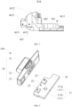
FIG. 3 is a partial structural schematic view illustrating cooperation of a non-contact switch and a middle frame of the electronic device ofFIG. 1 . -
FIG. 4 is a three-dimensional structural schematic view of the middle frame ofFIG. 3 . -
FIG. 5 is a cross-sectional structural schematic view of the middle frame ofFIG. 4 in a B-B direction. -
FIG. 6 is a three-dimensional structural schematic view of the non-contact switch ofFIG. 3 in some embodiments. -
FIG. 7 is a schematic view illustrating magnetic field intensity changes in various directions of a first Hall sensor when a sliding member slides along a preset direction relative to a fixed member inFIG. 6 . -
FIG. 8 is a schematic view illustrating magnetic field intensity changes in various directions of a second Hall sensor when the sliding member slides along the preset direction relative to the fixed member inFIG. 6 . -
FIG. 9 is a schematic view illustrating a relationship between magnetic field changes of the first Hall sensor and the second Hall sensor and a sliding distance of the sliding member relative to the fixed member. -
FIG. 10 is a three-dimensional structural schematic view of the non-contact switch ofFIG. 3 in some embodiments. -
FIG. 11 is a structural schematic view of the non-contact switch ofFIG. 10 . -
FIG. 12 is a structural schematic view of the non-contact switch ofFIG. 11 in some embodiments. -
FIG. 13 is a cross-sectional schematic view of a magnetoresistive sensor of a sensor module of a displacement measurement structure ofFIG. 11 . -
FIG. 14 is an axial schematic view illustrating a resistance of the magnetoresistive sensor varying with an external magnetic field. -
FIG. 15 is a circuit schematic view of a processor of the non-contact switch ofFIG. 11 . -
FIG. 16 is a structural schematic view of an electronic device in some embodiments of the present disclosure. - The present disclosure may be explained in detail by combining the accompanying drawings and embodiments. The following embodiments are only used to illustrate the present disclosure, but do not limit the scope of the present disclosure. Similarly, the following embodiments are only a part of the embodiments of the present disclosure, and not all embodiments. All other embodiments obtained by those of ordinary skill in the art without creative effort are within the scope of the present disclosure.
- The reference to "embodiment" in the present disclosure means that, specific features, structures, or characteristics described in conjunction with some embodiments may be included in at least one embodiment of the present disclosure. The phrase appearing in various positions in the specification does not necessarily refer to the same embodiment, nor is it an independent or alternative embodiment that is mutually exclusive with other embodiments. Those of ordinary skill in the art explicitly and implicitly understand that the embodiments described in the present disclosure can be combined with other embodiments.
- The terms "first", "second", and "third" in the present disclosure are only configured to describe and cannot be understood as indicating or implying relative importance or implicit indicating the quantity of technical features indicated. Therefore, features that are defined as "first", "second", and "third" may explicitly or implicitly include at least one of these features. In the description of the present disclosure, "multiple" means at least two, such as two, three, etc., unless otherwise expressly and specifically qualified.
- As illustrated in
FIGS. 1 and 2, FIG. 1 is a front schematic view of an electronic device in some embodiments of the present disclosure, andFIG. 2 is a cross-sectional schematic view of the electronic device ofFIG. 1 in an A-A direction.FIG. 1 is a three-dimensional schematic view of the electronic device in some embodiments of the present disclosure. The present disclosure provides anelectronic device 1000. Theelectronic device 1000 may be any one (only one form is shown as an example inFIG. 1 ) of various types of computer system devices that are mobile or portable and perform wireless communication. Theelectronic device 1000 may be a mobile phone or a smart phone (such as a phone based on an iPhone TM or an Android TM), a portable gaming device (such as a Nintendo DS TM), a PlayStation Portable TM, a Gameboy Advance TM, or the iPhone TM), a laptop computer, a PDA, a portable internet device, a music player, a data storage device, other handheld devices, or a headphone, etc. Theelectronic device 1000 may also be other wearable devices that need to be charged (such as an electronic bracelet, an electronic necklace, an electronic device, or an HMD of a smart watch). - The
electronic device 1000 may also be any one of multiple electronic devices. Theelectronic device 1000 includes but not limited to, a cellular phone, a smart phone, other wireless communication devices, a personal digital assistant, an audio player, other media players, a music recorder, a video recorder, other media recorders, a radio, a medical device, a vehicle transport device, a calculator, a programmable remote control, a pager, the laptop computer, a desktop computer, a printer, a netbook computer, a personal digital assistant (PDA), a portable multimedia player (PMP), a motion picture experts group (MPEG-1 or MPEG-2) audio layer 3 (MP3) player, a portable medical device, a digital camera or their combinations, etc. - In some embodiments, the
electronic device 1000 can perform multiple functions (such as playing music, displaying videos, storing images, and receiving and sending phone calls). If necessary, theelectronic device 1000 may be a compact portable device, such as the cellular phone, the media player, other handheld devices, a wristwatch device, a pendant device, or an earpiece device, etc. - As illustrated in
FIG. 3, FIG. 3 is a partial structural schematic view illustrating cooperation of a non-contact switch and a middle frame of the electronic device ofFIG. 1 . Theelectronic device 1000 may include amiddle frame 400, aback cover 300, adisplay screen 200, and anon-contact switch 100. Theback cover 300 is connected to a side surface of themiddle frame 400, so that theback cover 300 is connected to themiddle frame 400. Thedisplay screen 200 is disposed on a surface of themiddle frame 400 away from theback cover 300. Themiddle frame 400 may be connected to theback cover 300 and thedisplay screen 200. Themiddle frame 400, theback cover 300, and thedisplay screen 200 are enclosed to form astorage space 4001. Thestorage space 4001 can be configured to accommodate structural components, such as a camera module, a mainboard, and a battery, etc., so that theelectronic device 1000 can achieve corresponding functions. The structural components, such as thedisplay screen 200, the camera module, etc., are electrically connected to the mainboard, the battery, etc. through a flexible printed circuit board (FPC), respectively. Therefore, the structural components can receive power supply from the battery and execute corresponding instructions under the control of the mainboard. Anon-contact switch 100 is disposed on themiddle frame 400 and electrically connected to the mainboard. Thenon-contact switch 100 is configured to allow theelectronic device 1000 to be in a ring, mute, or do-not-disturb mode, or to control volume up, volume down, or volume hold, etc., which are not listed here. - The
middle frame 400 may be configured to allow various electronic components required for theelectronic device 1000 to be installed on themiddle frame 400. Themiddle frame 400 may be enclosed together with theback cover 300 and thedisplay screen 200 to form thestorage space 4001. Thestorage space 4001 may be configured to accommodate electronic components such as an optical sensor, etc., so as to achieve functions such as fingerprint unlocking, automatic screen turning off, and brightness self-adjustment, etc. Thestorage space 4001 may be configured to accommodate the electronic components such as a microphone, a speaker, a flashlight, a circuit board, and a battery, so as to achieve functions such as voice communication, audio playback, and lighting, etc. - As illustrated in
FIGS. 4 and5 ,FIG. 4 is a three-dimensional structural schematic view of the middle frame ofFIG. 3 , andFIG. 5 is a cross-sectional structural schematic view of the middle frame ofFIG. 4 in a B-B direction. In some embodiments, themiddle frame 400 may include amiddle plate 401 and aside frame 402, and theside frame 402 extends from an edge of themiddle plate 401. Themiddle plate 401 and theside frame 402 are enclosed to form anaccommodating chamber 4011. The camera module, the mainboard, the battery, and other structures are accommodated in theaccommodating chamber 4011. - The
side frame 402 may define a slidinggroove 403, and partial structure of thenon-contact switch 100 is slidably connected to the slidinggroove 403, and partial structure of thenon-contact switch 100 is accommodated in theaccommodating chamber 4011 and fixed on themiddle plate 401. - In some embodiments, the
side frame 402 may include afirst surface 4021 and asecond surface 4022 that are disposed adjacent to each other. Thefirst surface 4021 is disposed away from theaccommodating chamber 4011, and thesecond surface 4022 is approximately parallel to themiddle plate 401. Thefirst surface 4021 defines a slidingslot 4031, and thesecond surface 4022 defines acard slot 4032 that is communicated with the slidingslot 4031. The slidingslot 4031 and thecard slot 4032 form the slidinggroove 403. - In some embodiments, the
back cover 300 may be abutted against thesecond surface 4022 of theside frame 402, so that theback cover 300 can seal thesecond groove 4032 and prevent external water, dust, etc. from entering theaccommodating chamber 4011 through the slidingslot 4031 and the card slot 4032 (i.e. the sliding groove 403). In addition, theback cover 300 is further configured to protect the mainboard, the battery, and other structures in thestorage space 4001. - The
display screen 200 can be configured to provide image display function for theelectronic device 1000. When a user uses a shooting function of theelectronic device 1000, thedisplay screen 200 can present an imaging picture of the camera module for the user to observe and operate. - As illustrated in
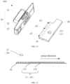
FIG. 6, FIG. 6 is a three-dimensional structural schematic view of the non-contact switch ofFIG. 3 in some embodiments. Thenon-contact switch 100 may include a fixedmember 10, a slidingmember 20, and aprocessor 30. The slidingmember 20 can be slidable relative to the fixedmember 10. In some embodiments, the fixedmember 10 may include asensor module 11, and the slidingmember 20 may include amagnetic head 23. Themagnetic head 23 moves relative to thesensor module 11, so that thesensor module 11 can sense a position of themagnetic head 23 relative to the sensor module 11 (i.e., a position of the slidingmember 20 relative to the fixed member 10). Theprocessor 30 is electrically connected to thesensor module 11. Theprocessor 30 allows thenon-contact switch 100 to be in a corresponding operating mode according to the position of the slidingmember 20 relative to the fixedmember 10. - In some embodiments, the fixed
member 10 may be spaced apart from the slidingmember 20, that is, the fixedmember 10 and the slidingmember 20 may be disposed in a non-contact manner. In some embodiments, the fixedmember 10 is accommodated in thestorage space 4001 and fixed to themiddle plate 401. The slidingmember 20 is clamped and accommodated in the slidinggroove 403, so that the slidingmember 20 can slide along a preset direction in the slidinggroove 403. Therefore, theelectronic device 1000 can be controlled to enter the corresponding operating mode without the slidingmember 20 directly contacting with the fixedmember 10. That is, for thenon-contact switch 100 in the present disclosure, it is not necessary to consider sealing of theelectronic device 1000, thereby making the structure of theelectronic device 1000 simpler. - In some embodiments, the sliding
member 20 may further include a slidingpart 21 and a clampingpart 22 connected to the slidingpart 21, and themagnetic head 23 is disposed on the clampingpart 22. The slidingpart 21 is slidably connected to the slidingslot 4031 and protrudes from thefirst surface 4021, so as to facilitate sliding of the slidingmember 20 by the user. Thecard holder 22 is clamped in thecard slot 4032. On the one hand, the slidingpart 21 is prevented from being detached from the slidingslot 4031, improving reliability of a connection between the slidingpart 21 and themiddle frame 400. On the other hand, themagnetic head 23 is fixed, so that themagnetic head 23 faces thestorage space 4001 and is adjacent to the fixedmember 10. - In some embodiments, the
sensor module 11 may include at least oneHall sensor 111, theHall sensor 111 may be disposed along the preset direction. When the slidingmember 20 slides relative to the fixedmember 10, theHall sensor 111 can detect a magnetic field strength of themagnetic head 23 and determine the position of the slidingmember 20 relative to the fixedmember 10 according to the magnetic field strength of themagnetic head 23. - In some embodiments, the
sensor module 11 may include two Hall sensors 111 (afirst Hall sensor 111a and asecond Hall sensor 111b), and thefirst Hall sensor 111a and thesecond Hall sensor 111b are spaced apart from each other along the preset direction. When themagnetic head 23 is disposed corresponding to the first Hall sensor 11a, that is, when the slidingmember 20 is located at a first position Z1 of the fixedmember 10, thenon-contact switch 100 can be in a first operating mode. When themagnetic head 23 is located between thefirst Hall sensor 111a and thesecond Hall sensor 111b, that is, when the slidingmember 20 is located at a second position Z2 of the fixedmember 10, the non-contact switch can be in a second operating mode. When themagnetic head 23 is disposed corresponding to thesecond Hall sensor 111b, that is, when the slidingmember 20 is located at a third position Z3 of the fixedmember 10, thenon-contact switch 100 is in a third operating mode. - In some embodiments, when the
non-contact switch 100 is in the first operating mode, theelectronic device 1000 can be in the ring mode. When thenon-contact switch 100 is in the second operating mode, theelectronic device 1000 can be in the do-not-disturb mode. When thenon-contact switch 100 is in the third operating mode, theelectronic device 1000 can be in the mute mode. In some embodiments, when thenon-contact switch 100 is in the first operating mode, theelectronic device 1000 can be in a volume up mode. When thenon-contact switch 100 is in the second operating mode, theelectronic device 1000 can be in a volume hold mode. When thenon-contact switch 100 is in the third operating mode, theelectronic device 1000 can be in a volume down mode. - As illustrated in
FIGS. 7 to 9. FIG. 7 is a schematic view illustrating magnetic field intensity changes in various directions of a first Hall sensor when a sliding member slides along a preset direction relative to a fixed member inFIG. 6 ,FIG. 8 is a schematic view illustrating magnetic field intensity changes in various directions of a second Hall sensor when the sliding member slides along the preset direction relative to the fixed member inFIG. 6 , andFIG. 9 is a schematic view illustrating a relationship between magnetic field changes of the first Hall sensor and the second Hall sensor and a sliding distance of the sliding member relative to the fixed member. In some embodiments, as illustrated inFIGS. 7-9 , a single axis Hall sensor is only sensitive to the magnetic field strength in a Z-axis direction, therefore, the Hall sensor only needs to detect the magnetic field strength in the Z-axis direction. - As illustrated in
FIGS. 7 to 9 , when the slidingmember 20 is located at the first position Z1 of the fixedmember 10, the magnetic field strength measured by thefirst Hall sensor 111a is the largest. As illustrated inFIG. 8 , when the slidingmember 20 is located at the third position Z3 of the fixedmember 10, the magnetic field strength measured by thesecond Hall sensor 111b is the largest. When the slidingmember 20 is located at the second position Z2 of the fixedmember 10, themagnetic head 23 is located between thefirst Hall sensor 111a and thesecond Hall sensor 111b, as illustrated inFIG. 9 . - As illustrated in
FIGS. 7 to 9 , when the slidingmember 20 is located at the first position Z1, second position Z2, and third position Z3 of the fixedmember 10, a magnetic field strength difference betweenadjacent Hall sensors 111 is only 5mT. Considering shaking factors at different positions, the solution can only withstand approximately 3mT of external magnetic field interference. When the external magnetic field interference exceeds 3mT, thenon-contact switch 100 can be abnormal, affecting the normal function of theelectronic device 1000. - As illustrated in
FIGS. 10 and 11 , in some embodiments, thesensor module 11 includes multiplemagnetoresistive sensors 112 disposed along the preset direction, and multiplemagnetoresistive sensors 112 are sequentially connected in series. The slidingmember 20 moves relative to the fixedmember 10 along the preset direction, so that themagnetic head 23 sequentially passes by at least onemagnetoresistive sensor 112. Themagnetic head 23 magnetizes themagnetoresistive sensor 112 that is passed by themagnetic head 23 and changes a resistance value of themagnetoresistive sensor 112 that is passed by themagnetic head 23, thereby changing a total resistance value of thesensor module 11. Theprocessor 30 determines the position of the slidingmember 20 relative to the fixedmember 10 according to the total resistance of thesensor module 11, and makes thenon-contact switch 100 be in the corresponding operating mode. Themagnetoresistive sensor 112 passed by themagnetic head 23 only includes themagnetoresistive sensor 112 passed during a movement process of themagnetic head 23, and does not include the current correspondingmagnetoresistive sensor 112. - As illustrated in
FIG. 12, FIG. 12 is a structural schematic view of the non-contact switch ofFIG. 11 in some embodiments. When the slidingmember 20 is located at the first position Z1 of the fixedmember 10, the total resistance value of thesensor module 11 is a first total resistance value. When the slidingmember 20 is located at the second position Z2 of the fixedmember 10, the total resistance value of thesensor module 11 is a second total resistance value. When the slidingmember 20 is located at the third position Z3 of the fixedmember 10, the total resistance value of thesensor module 11 is a third total resistance value. The second total resistance value is greater than the first total resistance value and less than the third total resistance value. It can be understood that a distance of the slidingmember 20 relative to the fixedmember 10 is mapped one-to-one with the total resistance value of thesensor module 11. That is, the distance of the slidingmember 20 relative to the fixedmember 10 is linearly related to the total resistance value of thesensor module 11. Theprocessor 30 determines a moving distance of the slidingmember 20 relative to the fixedmember 10 according to the total resistance value of thesensor module 11. That is, theprocessor 30 determines the position of the slidingmember 20 relative to the fixedmember 10, so that thenon-contact switch 100 is in the corresponding operating mode. - In some embodiments, when the total resistance value of the
sensor module 11 is a first resistance value, that is, when the slidingmember 20 is located at the first position Z1 of the fixedmember 10, thenon-contact switch 100 can be in the first operating mode. When the total resistance value of thesensor module 11 is a second resistance value, that is, when the slidingmember 20 is located at the second position Z2 of the fixedmember 10, thenon-contact switch 100 can be in the second operating mode. When the total resistance value of thesensor module 11 is a third resistance value, that is, when the slidingmember 20 is located at the third position Z3 of the fixedmember 10, thenon-contact switch 100 can be in the third operating mode. - In some embodiments, when the
non-contact switch 100 is in the first operating mode, theelectronic device 1000 can be in the ring mode. When thenon-contact switch 100 is in the second operating mode, theelectronic device 1000 can be in the do-not-disturb mode. When thenon-contact switch 100 is in the third operating mode, theelectronic device 1000 can be in the mute mode. In some embodiments, when thenon-contact switch 100 is in the first operating mode, theelectronic device 1000 can be in the volume up mode. When thenon-contact switch 100 is in the second operating mode, theelectronic device 1000 can be in the volume hold mode. When thenon-contact switch 100 is in the third operating mode, theelectronic device 1000 can be in the volume down mode. - As illustrated in
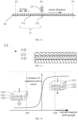
FIGS. 13, FIG. 13 is a cross-sectional schematic view of a magnetoresistive sensor of a sensor module of a displacement measurement structure ofFIG. 11 . In some embodiments, themagnetoresistive sensor 112 is a tunnel magnetoresistance effect (TMR) memory magnetoresistive sensor. Themagnetoresistive sensor 112 is a thin film component made by advanced film making technology. Themagnetoresistive sensor 112 may include abarrier layer 1121, a first magnetic layer 1122 (i.e., a fixed layer), and a second magnetic layer 1123 (i.e., a free layer). The firstmagnetic layer 1122 and the secondmagnetic layer 1123 are located on two opposite side surfaces of thebarrier layer 1121, respectively. A magnetic field direction of the firstmagnetic layer 1122 is fixed, and the secondmagnetic layer 1123 can be magnetized by an external magnetic field (i.e., the magnetic head 23). A magnetic field direction of the secondmagnetic layer 1123 changes according to a magnetic field direction of the external magnetic field. In some embodiments, the magnetic field direction of the secondmagnetic layer 1123 is determined by the magnetic field direction of the firstmagnetic layer 1122 and a moving direction of themagnetic head 23 relative to thesensor module 11. In some embodiments, the firstmagnetic layer 1122 is disposed away from themagnetic head 23, so as to reduce influence of themagnetic head 23 on the firstmagnetic layer 1122. The secondmagnetic layer 1123 is disposed adjacent to themagnetic head 23, so that themagnetic head 23 can magnetize the secondmagnetic layer 1123 conveniently and quickly. - In some embodiments, when the magnetic field direction of the second
magnetic layer 1123 is consistent with that of the firstmagnetic layer 1122, a resistance of themagnetoresistive sensor 112 is the smallest, and a current flowing through thebarrier layer 1121 is the largest. At this time, themagnetoresistive sensor 112 has the first resistance value. When the magnetic field direction of the secondmagnetic layer 1123 is opposite (i.e., antiparallel) to that of the firstmagnetic layer 1122, the resistance of themagnetoresistive sensor 112 extremely increases, and almost no current flows through thebarrier layer 1121. At this time, themagnetoresistive sensor 112 has the second resistance value. The magnetic field direction of the secondmagnetic layer 1123 is consistent or opposite to the moving direction of themagnetic head 23. In some embodiments, the magnetic field direction of the secondmagnetic layer 1123 can be consistent with the moving direction of the magnetic head 162, and themagnetoresistive sensor 112 has the first resistance value. The magnetic field direction of the secondmagnetic layer 1123 can be opposite to the moving direction of the magnetic head 162, and themagnetoresistive sensor 112 has the second resistance value. The first resistance value is less than the second resistance value. - As illustrated in
FIG. 14, FIG. 14 is an axial schematic view illustrating a resistance of the magnetoresistive sensor varying with an external magnetic field. As illustrated inFIG. 14 , when the magnetic field direction of the secondmagnetic layer 1123 is consistent with the magnetic field direction of the firstmagnetic layer 1122 under a magnetization effect of the external magnetic field, and a magnetic field strength of the external magnetic field is greater than a preset magnetic field strength (i.e., on a left side of a -OP value ofFIG. 14 ), themagnetoresistive sensor 112 has the first resistance value RL ( i.e., the minimum resistance value). Even if the magnetic field strength of the external magnetic field continues to increase, the resistance value of themagnetoresistive sensor 112 is still the first resistance value RL . When the magnetic field direction of the secondmagnetic layer 1123 is opposite to the magnetic field direction of the firstmagnetic layer 1122 under the magnetization effect of the external magnetic field, and the magnetic field strength of the external magnetic field is greater than the preset magnetic field strength (i.e., on a right side of a +OP value ofFIG. 14 ), themagnetoresistive sensor 112 has the second resistance value Rh (i.e., the maximum resistance value). Even if the magnetic field strength of the external magnetic field continues to increase, the resistance value of themagnetoresistive sensor 112 is still the second resistance value Rh . That is, when the magnetic field strength of themagnetic head 23 is greater than the preset magnetic field strength, the moving direction of themagnetic head 23 relative to thesensor module 11 changes, and the resistance value of themagnetoresistive sensor 112 that is passed by themagnetic head 23 can be switched between the first resistance value and the second resistance value. In some embodiments, when themagnetic head 23 moves along the preset direction and the magnetic field strength of themagnetic head 23 is greater than the preset magnetic field strength, themagnetoresistive sensor 112 has the first resistance value RL . When themagnetic head 23 moves along the opposite direction of the preset direction and the magnetic field strength of themagnetic head 23 is greater than the preset magnetic field strength, themagnetoresistive sensor 112 has the second resistance value Rh . - When the magnetic field strength of the external magnetic field is less than the preset magnetic field strength, that is, between the -OP value and the +OP value, the resistance value of the
magnetoresistive sensor 112 roughly changes linearly. It can be understood that the magnetic field strength of themagnetic head 23 is usually greater than the preset magnetic field strength, therefore, a situation where the magnetic field strength of the external magnetic field is between the -OP value and the +OP value can be omitted. - In some embodiments, when the magnetic field strength of the
magnetic head 23 is greater than the preset magnetic field strength, that is, outside a range from the -OP value to the +OP value, the resistance value of themagnetoresistive sensor 112 can be maintained in a memory resistance state. That is, even if there is no power supply, the resistance value of themagnetoresistive sensor 112 does not change, and the resistance value of themagnetoresistive sensor 112 has a physical memory function. In some embodiments, when the magnetic field direction of the secondmagnetic layer 1123 is consistent with the magnetic field direction of the firstmagnetic layer 1122 under the magnetization effect of the external magnetic field, and the magnetic field strength of the external magnetic field is greater than the preset magnetic field strength (i.e., on the left side of the -OP value ofFIG. 14 ), themagnetoresistive sensor 112 has the first resistance value RL ( i.e., the minimum resistance value). When the magnetic field direction of the secondmagnetic layer 1123 is opposite to the magnetic field direction of the firstmagnetic layer 1122 under the magnetization effect of the external magnetic field, and the magnetic field strength of the external magnetic field is greater than the preset magnetic field strength (i.e., on the right side of the +OP value ofFIG. 14 ), themagnetoresistive sensor 112 has the second resistance value Rh (i.e., the maximum resistance value). The magnetic field strength of the external magnetic field is usually much less than the magnetic field strength applied by themagnetic head 23. In some embodiments, the magnetic field strength applied by themagnetic head 23 is usually 10 times or 100 times that of the external interference magnetic field. As long as the strength of the external interference magnetic field is less than the preset magnetic field strength, the external interference magnetic field has no effect on accuracy of a displacement measurement structure. That is, compared with related arts, anti-magnetic interference capability of the displacement measurement structure in the embodiments of the present disclosure is improved by more than 10 times. - As illustrated in
FIG. 12 , in some embodiments, the first position Z1 and the third position Z3 are located at two opposite ends of the module sensor, and the second position Z2 is located in a middle position between the first position Z1 and the third position Z3. When a distance between the first position Z1 and the second position Z2 is approximately 1.4mm, and a distance between the second position Z2 and the third position Z3 is 1.4mm, a length of thesensor module 11 is greater than 2.8mm. - Taking the
sensor module 11 with a length of 3.0mm (actual effective monitoring length of 2.9mm) as an example, thesensor module 11 may include 30magnetoresistive sensors 112, a distance between centers of two adjacentmagnetoresistive sensors 112 is 0.1mm. In some embodiments, arranged from left to right, a position of a first magnetoresistive sensor corresponds to a 0mm position, a position of a second magnetoresistive sensor corresponds to a 0.1mm position, and so on. A position of a 30th magnetoresistive sensor corresponds to a 2.9mm position. That is, multiplemagnetoresistive sensors 112 are arranged at equal intervals along the preset direction, so that an effective monitoring distance of thesensor module 11 is 0.1mm * (30-1)=2.9mm, and displacement resolution of thesensor module 11 is 0.1mm. - The first position Z1 is located at the 0.1mm position of the sensor module 11 (i.e., as illustrated in
FIG. 12 , arranged from left to right, the position of the second magnetoresistive sensor 112). The second position Z2 is located at a 1.5mm position of the sensor module 11 (i.e., as illustrated inFIG. 12 , arranged from left to right, the position of a 16th magnetoresistive sensor 112). The third position Z3 is located at the 2.9mm position of the sensor module 11 (i.e., as illustrated inFIG. 12 , arranged from left to right, the position of a 30thmagnetoresistive sensor 112; or arranged from right to left, the position of the first magnetoresistive sensor 112). - In some embodiments, when the
magnetic head 23 moves from a first end to a second end of thesensor module 11, that is, when themagnetic head 23 moves from the first position Z1 to the third position Z3, the resistance value of themagnetoresistive sensor 112 that passed by themagnetic head 23 is switched from the first resistance value RL to the second resistance value Rh and maintains memory. When themagnetic head 23 moves from the second end to the first end of thesensor module 11, that is, when themagnetic head 23 moves from the third position Z3 to the first position Z1, the resistance value of themagnetoresistive sensor 112 that passed by themagnetic head 23 is switched from the second resistance value Rh to the first resistance value RL and maintains memory. That is, the relative displacement between themagnetic head 23 and thesensor module 11 is linearly related to the resistance change value of thesensor module 11. In some embodiments, the greater the resistance change of thesensor module 11, the moremagnetoresistive sensors 112 themagnetic head 23 passes by, and the greater the relative displacement between themagnetic head 23 and thesensor module 11. In some embodiments, when the magnetic head 23 moves from the first position Z1 to the second position Z2, as illustrated inFIG. 12 , the magnetic head 23 passes by the second magnetoresistive sensor 112 to the 16th magnetoresistive sensor 112 that are arranged from left to right, 1.4/0.1=14, and the resistance values of fourteen magnetoresistive sensors 112 on the left side are switched from the first resistance value RL to the second resistance value Rh, while the resistance values of the magnetoresistive sensors 112 at other positions are still the first resistance value RL . Therefore, an overall resistance of the sensor module 11 is R=15 Rh +15 RL . In some embodiments, when the magnetic head 23 moves from the second position Z2 to the first position Z1, as illustrated inFIG. 12 , the magnetic head 23 passes by a 15th magnetoresistive sensor 112 to the second magnetoresistive sensor 112 that are arranged from left to right, 1.4/0.1=14, the resistance values of the fourteen magnetic sensors 112 on the left side are switched from the second resistance value Rh to the first resistance value RL , while the resistance values of the magnetoresistive sensors 112 (fifteen magnetoresistive sensors 112) at other positions are still the first resistance value RL . Only the magnetoresistive sensor 112 (i.e. the first one from left to right) on the left side of the first position Z1 still has the last memory, and the resistance value is the second resistance value Rh . Therefore, the overall resistance of the sensor module 11 is R=1 Rh +29 RL . - In some embodiments, regardless of whether the
magnetic head 23 moves to the left or the right, themagnetoresistive sensor 112 corresponding to the current position of themagnetic head 23 does not change. In some embodiments, the magnetic field direction of themagnetic head 23 is perpendicular to the secondmagnetic layer 1123 of themagnetoresistive sensor 112, so that the magnetic field direction of the secondmagnetic layer 1123 of thesensor module 11 magnetized by themagnetic head 23 is perpendicular to the magnetic field direction of the firstmagnetic layer 1122. That is, the magnetic field direction of the secondmagnetic layer 1123 is neither the same as nor opposite to that of the firstmagnetic layer 1122, and the resistance value of themagnetoresistive sensor 112 does not change. When themagnetic head 23 moves to the left or the right, on a side in the moving direction of themagnetic head 23 the magnetic field direction of themagnetic head 23 is either consistent with or opposite to the magnetic field direction of the secondmagnetic layer 1123 of themagnetoresistive sensor 112, so that the resistance of themagnetoresistive sensor 112 passed by themagnetic head 23 can change. - That is, when the sliding
member 20 is located at the first position Z1 of the fixed member 10 (i.e., the 0.1mm position of the sensor module 11), the overall resistance of thesensor module 11 is R=1 Rh +29 RL . When the slidingmember 20 is located at the second position Z2 of the fixed member 10 (i.e., the 1.5mm position of the sensor module 11), the overall resistance of thesensor module 11 is R=15 R h +15 RL . When the slidingmember 20 is located at the third position Z3 of the fixed member 10 (i.e., the 2.9mm position of the sensor module 11), the overall resistance of thesensor module 11 is R=29 R h + 1 RL . - In some embodiments, when the
magnetic head 23 is at the first position Z1 and the 0.1mm position, the overall resistance of thesensor module 11 is R=1 * 600+29 * 300=9.3KΩ. When themagnetic head 23 is at the second position Z2 and the 1.5mm position, the overall resistance of thesensor module 11 is R=15 * 300+15 * 600=13.5KQ. When themagnetic head 23 is at the third position Z3 and the 2.9mm position, the overall resistance of thesensor module 11 is R=29 * 600+1 * 300=17.7KΩ. - In some embodiments, considering that a mating position tolerance between adjacent positions is 0.2mm, when the resistance ranges from 9.9KΩ to 9KQ, it is judged as the first position Z1. When the resistance ranges from 14.1KΩ to 12.9KQ, it is judged as the second position Z2. When the resistance ranges from 18KΩ to 17.1KΩ, it is judged as the third position Z3. A large gap between the resistance values of the
sensor module 11 when the slidingmember 20 is located at different positions, it is easy to distinguish. - In some embodiments, the magnetic field strength applied by the
magnetic head 23 is usually 10 times or 100 times that of the external interference magnetic field. As long as the strength of the external interference magnetic field is less than the preset magnetic field strength, the external interference magnetic field has no effect on the accuracy of the displacement measurement structure. That is, the displacement measurement structure in the embodiments of the present disclosure has excellent anti-magnetic interference capability. - In some embodiments when the
magnetoresistive sensors 112 are disposed at equal intervals, the resistance change values of themagnetoresistive sensors 112 are linearly related to the relative displacements between themagnetic head 23 and thesensor module 11. In some embodiments, the first position Z1, the second position Z2, and the third position Z3 are disposed at equal intervals. - In some embodiments, the distance between adjacent
magnetoresistive sensors 112 may be equal, unequal, or partially equal, without specific limitations. Correspondingly, the first position Z1, the second position Z2, and the third position Z3 may be disposed at equal intervals or according to requirements, without specific restrictions. - As illustrated in
FIG. 15, FIG. 15 is a circuit schematic view of a processor of the non-contact switch ofFIG. 11 . Theprocessor 30 is configured to measure the total resistance of thesensor module 11. In some embodiments, theprocessor 30 may include a fixedresistor 31 and anexternal power supply 32. The fixedresistor 31 is connected in series with thesensor module 11. A positive pole of theexternal power supply 32 is electrically connected to an external sensor, and a negative pole of theexternal power supply 32 is electrically connected to the fixedresistor 31. By measuring voltage division of the fixedresistor 31, the total resistance value of the sensor can be determined, thereby determining the relative displacement of themagnetic head 23 relative to thesensor module 11. - The
sensor module 11 may further include anoperational amplifier 33 and an analog-to-digital converter 34. Due to high resistance of thesensor module 11, a voltage division value of the fixedresistor 31 is relatively small. Theoperational amplifier 33 is configured to amplify voltages of two terminals of the fixedresistor 31, making the measurement of the resistance value of thesensor module 11 more accurate. The analog-to-digital converter 34 is configured to convert an analog signal measured by theoperational amplifier 33 into a digital signal. - The
magnetic head 23 is one of a permanent magnet and an electromagnet. In some embodiments, a material of themagnetic head 23 is the permanent magnet, so as to reduce electrical connections with other structures and simplify the structure of theelectronic device 1000. - In some embodiments, the
processor 30 may be one of a circuit board or a flexible circuit board. Theprocessor 30 may be integrated with the sensor module and fixed on the middle frame 400 (such as the middle plate or the side frame), or theprocessor 30 may be a part of the mainboard, without specific limitations. - In the
non-contact switch 100 provided by the embodiments of the present disclosure, the slidingmember 20 is spaced apart from the fixedmember 10, and the slidingmember 20 moves along the preset direction relative to the fixedmember 10. By disposing thesensor module 11 on the fixedmember 10 and disposing themagnetic head 23 on the slidingmember 20, thesensor module 11 can determine the position of the slidingmember 20 relative to the fixedmember 10. Theprocessor 30 makes thenon-contact switch 100 be in the corresponding operating mode according to the position of the slidingmember 20 relative to the fixedmember 10. In thenon-contact switch 100 provided by the present disclosure, the slidingmember 20 does not need to be in direct contact with the fixedmember 10, which is beneficial for improving the sealing performance of theelectronic device 1000. - As illustrated in
FIG. 16, FIG. 16 is a structural schematic view of an electronic device in some embodiments of the present disclosure. The present disclosure further provides anelectronic device 800. Theelectronic device 800 includes an RF (radio frequency)circuit 810, amemory 820, aninput unit 830, a display unit 8, asensor 850, anaudio circuit 860, aWiFi module 870, aprocessor 880, and apower supply 890, etc. TheRF circuit 810, thememory 820, theinput unit 830, the display unit 8, thesensor 850, theaudio circuit 860, and theWiFi module 870 are connected to theprocessor 880, respectively. Thepower supply 890 is configured to provide electrical energy to the entireelectronic device 800. - In some embodiments, the
RF circuit 810 is configured for receiving and transmitting signals. Thememory 820 is configured to store data instruction information. Theinput unit 830 is configured for inputting information, and theinput unit 830 may include atouch panel 831 andother input devices 832 such as an operation button. The display unit 8 may include adisplay panel 841, etc. Thesensor 850 includes an infrared sensor, a laser sensor, etc., and configured to detect a user proximity signal, a distance signal, etc. Aspeaker 861 and amicrophone 862 are connected toprocessor 880 through theaudio circuit 860, and configured for receiving and transmitting sound signals. TheWiFi module 870 is configured for receiving and transmitting WiFi signals, and theprocessor 880 is configured for processing data information of the electronic device. - The above embodiments are only some embodiments of the present disclosure, and are not intended to limit the protection scope of the present disclosure. Any equivalent structure or equivalent flow transformation made by using the contents and the accompanying drawings of the present disclosure, or directly or indirectly applied to other related technical fields, is included in the protection scope of the present disclosure.
Claims (20)
- A non-contact switch, characterized by comprising:a fixed member, comprising a sensor module;a sliding member, spaced apart from the fixed member and movable along a preset direction relative to the fixed member; wherein the sliding member comprises a magnetic head, and the magnetic head at least partially overlaps with the sensor module, so that the sensor module is able to determine a position of the sliding member relative to the fixed member; anda processor, electrically connected to the sensor module; wherein the processor makes the non-contact switch be in a corresponding operating mode according to the position of the sliding member relative to the fixed member.
- The non-contact switch according to claim 1, wherein the sensor module comprises a plurality of magnetoresistive sensors disposed along the preset direction, and the plurality of magnetoresistive sensors are sequentially connected in series; the sliding member moves relative to the fixed member along the preset direction, so that the magnetic head sequentially passes by at least one magnetoresistive sensor; the magnetic head magnetizes the at least one magnetoresistive sensor that is passed by the magnetic head and changes a resistance value of the at least one magnetoresistive sensor that is passed by the magnetic head, so that a total resistance value of the sensor module changes; and the processor determines the position of the sliding member relative to the fixed member according to the total resistance value of the sensor module, and makes the non-contact switch be in the corresponding operating mode.
- The non-contact switch according to claim 2, wherein the plurality of magnetoresistive sensors are disposed at equal intervals.
- The non-contact switch according to claim 3, wherein when the sliding member is located at a first position of the fixed member, the non-contact switch is in a first operating mode; when the sliding member is located at a second position of the fixed member, the non-contact switch is in a second operating mode; and when the sliding member is located at a third position of the fixed member, the non-contact switch is in a third operating mode.
- The non-contact switch according to claim 4, wherein the first position, the second position, and the third position are disposed at equal intervals along the preset direction.
- The non-contact switch according to any one of claims 2 to 5, wherein each of the plurality of magnetoresistive sensors comprises a barrier layer, a first magnetic layer, and a second magnetic layer; the barrier layer comprises two opposite side surfaces, the first magnetic layer is located on one of the two opposite side surfaces, and the second magnetic layer is located on the other of the two opposite side surfaces; the magnetic head is configured to magnetize the second magnetic layer, and a magnetic field strength of the magnetic head is greater than a preset magnetic field strength.
- The non-contact switch according to claim 6, wherein when a magnetic field direction of the second magnetic layer is consistent with that of the first magnetic layer, each of the plurality of magnetoresistive sensors has a first resistance value; and when the magnetic field direction of the second magnetic layer is opposite to that of the first magnetic layer, each of the plurality of magnetoresistive sensors has a second resistance value.
- The non-contact switch according to claim 7, wherein the magnetic field direction of the second magnetic layer is consistent or opposite to a moving direction of the magnetic head, and the first resistance value is less than the second resistance value.
- The non-contact switch according to claim 7, wherein the magnetic head is one of a permanent magnet and an electromagnet.
- The non-contact switch according to claim 1, wherein the sensor module comprises at least one Hall sensor disposed along the preset direction, and the at least one Hall sensor is configured to detect a magnetic field strength of the magnetic head and determine the position of the sliding member relative to the fixed member.
- An electronic device, characterized by comprising:a non-contact switch, comprising:a fixed member, comprising a sensor module;a sliding member, spaced apart from the fixed member and movable along a preset direction relative to the fixed member; wherein the sliding member comprises a magnetic head, and the magnetic head at least partially overlaps with the sensor module, so that the sensor module is able to determine a position of the sliding member relative to the fixed member; anda processor, electrically connected to the sensor module; wherein the processor makes the non-contact switch be in a corresponding operating mode according to the position of the sliding member relative to the fixed member; anda middle frame, comprising:a middle plate; anda side frame, wherein the side frame extends from an edge of the middle plate, the side frame and the middle plate are enclosed to define an accommodating chamber, the fixed member and the processor of the non-contact switch are accommodated in the accommodating chamber, and the sliding member of the non-contact switch is disposed on the side frame.
- The electronic device according to claim 11, wherein the sensor module comprises a plurality of magnetoresistive sensors disposed along the preset direction, and the plurality of magnetoresistive sensors are sequentially connected in series; the sliding member moves relative to the fixed member along the preset direction, so that the magnetic head sequentially passes by at least one magnetoresistive sensor; the magnetic head magnetizes the at least one magnetoresistive sensor that is passed by the magnetic head and changes a resistance value of the at least one magnetoresistive sensor that is passed by the magnetic head, so that a total resistance value of the sensor module changes; and the processor determines the position of the sliding member relative to the fixed member according to the total resistance value of the sensor module, and makes the non-contact switch be in the corresponding operating mode.
- The electronic device according to claim 12, wherein the plurality of magnetoresistive sensors are disposed at equal intervals.
- The electronic device according to claim 13, wherein when the sliding member is located at a first position of the fixed member, the non-contact switch is in a first operating mode; when the sliding member is located at a second position of the fixed member, the non-contact switch is in a second operating mode; and when the sliding member is located at a third position of the fixed member, the non-contact switch is in a third operating mode.
- The electronic device according to claim 14, wherein the first position, the second position, and the third position are disposed at equal intervals along the preset direction.
- The electronic device according to any one of claims 12 to 15, wherein each of the plurality of magnetoresistive sensors comprises a barrier layer, a first magnetic layer, and a second magnetic layer; the barrier layer comprises two opposite side surfaces, the first magnetic layer is located on one of the two opposite side surfaces, and the second magnetic layer is located on the other of the two opposite side surfaces; the magnetic head is configured to magnetize the second magnetic layer, and a magnetic field strength of the magnetic head is greater than a preset magnetic field strength.
- The electronic device according to claim 16, wherein when a magnetic field direction of the second magnetic layer is consistent with that of the first magnetic layer, each of the plurality of magnetoresistive sensors has a first resistance value; when the magnetic field direction of the second magnetic layer is opposite to that of the first magnetic layer, each of the plurality of magnetoresistive sensors has a second resistance value; and the magnetic field direction of the second magnetic layer is consistent or opposite to a moving direction of the magnetic head, and the first resistance value is less than the second resistance value.
- The electronic device according to claim 17, wherein the magnetic head is one of a permanent magnet and an electromagnet.
- The electronic device according to claim 11, wherein the sensor module comprises at least one Hall sensor disposed along the preset direction, and the at least one Hall sensor is configured to detect a magnetic field strength of the magnetic head and determine the position of the sliding member relative to the fixed member.
- The electronic device according to claim 11, wherein a surface of the side frame away from the accommodating chamber is recessed to define a sliding groove, and the sliding member is accommodated and slidable in the sliding groove, so that the sliding member slides along the preset direction relative to the fixed member.
Applications Claiming Priority (2)
| Application Number | Priority Date | Filing Date | Title |
|---|---|---|---|
| CN202211023899.XA CN115394582B (en) | 2022-08-24 | 2022-08-24 | Non-contact switches and electronic equipment |
| PCT/CN2023/101464 WO2024041144A1 (en) | 2022-08-24 | 2023-06-20 | Non-contact switch and electronic device |
Publications (2)
| Publication Number | Publication Date |
|---|---|
| EP4539076A1 true EP4539076A1 (en) | 2025-04-16 |
| EP4539076A4 EP4539076A4 (en) | 2025-10-08 |
Family
ID=84123389
Family Applications (1)
| Application Number | Title | Priority Date | Filing Date |
|---|---|---|---|
| EP23856236.7A Pending EP4539076A4 (en) | 2022-08-24 | 2023-06-20 | CONTACTLESS SWITCH AND ELECTRONIC DEVICE |
Country Status (4)
| Country | Link |
|---|---|
| US (1) | US20250140497A1 (en) |
| EP (1) | EP4539076A4 (en) |
| CN (1) | CN115394582B (en) |
| WO (1) | WO2024041144A1 (en) |
Families Citing this family (1)
| Publication number | Priority date | Publication date | Assignee | Title |
|---|---|---|---|---|
| CN115394582B (en) * | 2022-08-24 | 2026-04-24 | Oppo广东移动通信有限公司 | Non-contact switches and electronic equipment |
Family Cites Families (17)
| Publication number | Priority date | Publication date | Assignee | Title |
|---|---|---|---|---|
| CA1301884C (en) * | 1989-02-10 | 1992-05-26 | Ivan J. Garshelis | Magnetic position sensor |
| JPWO2008059914A1 (en) * | 2006-11-17 | 2010-03-04 | アルプス電気株式会社 | Magnetic detector and electronic apparatus using the same |
| JP5066603B2 (en) * | 2008-03-04 | 2012-11-07 | アルプス電気株式会社 | Magnetic sensor, magnetic encoder, and method of manufacturing magnetic sensor |
| JP4870226B2 (en) * | 2008-03-04 | 2012-02-08 | アルプス電気株式会社 | Position detection device |
| US10414033B2 (en) * | 2012-10-04 | 2019-09-17 | Black & Decker Inc. | Power tool hall effect mode selector switch |
| CN103808244A (en) * | 2014-02-28 | 2014-05-21 | 南京景曜智能科技有限公司 | Magnetic encoder for position measurement |
| CN103913709B (en) * | 2014-03-28 | 2017-05-17 | 江苏多维科技有限公司 | Single-chip three-axis magnetic field sensor and manufacturing method thereof |
| CN205910548U (en) * | 2016-08-04 | 2017-01-25 | 联想(北京)有限公司 | Electronic equipment |
| CN109819072A (en) * | 2018-12-05 | 2019-05-28 | 深圳市万普拉斯科技有限公司 | Electronic device and method for adjusting its working mode |
| CN109545602B (en) * | 2018-12-18 | 2020-10-09 | 深圳市万普拉斯科技有限公司 | Multi-section switch and electronic equipment |
| CN109326476A (en) * | 2019-01-03 | 2019-02-12 | 南昌黑鲨科技有限公司 | Toggle switch device and electronic equipment |
| CN114508993B (en) * | 2020-11-16 | 2024-10-01 | 精量电子(深圳)有限公司 | Magneto-resistance displacement measuring device |
| CN112747664B (en) * | 2020-12-30 | 2022-06-17 | 苏州博古特智造有限公司 | Linear magnetic resistance position sensor |
| CN214380853U (en) * | 2021-03-23 | 2021-10-08 | 科世达(上海)机电有限公司 | Non-contact electronic switch |
| CN113701615B (en) * | 2021-08-23 | 2024-08-16 | 上海米尔圣传感器有限公司 | Position sensor and position detection device |
| CN216599699U (en) * | 2022-01-06 | 2022-05-24 | 维沃移动通信有限公司 | Electronic device and electronic device assembly |
| CN115394582B (en) * | 2022-08-24 | 2026-04-24 | Oppo广东移动通信有限公司 | Non-contact switches and electronic equipment |
-
2022
- 2022-08-24 CN CN202211023899.XA patent/CN115394582B/en active Active
-
2023
- 2023-06-20 WO PCT/CN2023/101464 patent/WO2024041144A1/en not_active Ceased
- 2023-06-20 EP EP23856236.7A patent/EP4539076A4/en active Pending
-
2024
- 2024-12-30 US US19/005,259 patent/US20250140497A1/en active Pending
Also Published As
| Publication number | Publication date |
|---|---|
| WO2024041144A1 (en) | 2024-02-29 |
| CN115394582A (en) | 2022-11-25 |
| US20250140497A1 (en) | 2025-05-01 |
| CN115394582B (en) | 2026-04-24 |
| EP4539076A4 (en) | 2025-10-08 |
Similar Documents
| Publication | Publication Date | Title |
|---|---|---|
| US10459483B2 (en) | Functional device and mobile terminal | |
| KR100847652B1 (en) | Pointing device | |
| US20200103968A1 (en) | Button Providing Force Sensing and/or Haptic Output | |
| US20250140497A1 (en) | Switch and electronic device | |
| KR102258022B1 (en) | Sensor for determination relative position, electronic device including the same and method for determination relative position | |
| US20220342276A1 (en) | Camera module and optical device comprising same | |
| US10001808B1 (en) | Mobile device accessory equipped to communicate with mobile device | |
| US20200025965A1 (en) | Magnet position detection in a magnetic connector | |
| KR20220017323A (en) | Electronic device | |
| CN223652330U (en) | Switching mechanism | |
| US10599223B1 (en) | Button providing force sensing and/or haptic output | |
| EP1988690B1 (en) | Acoustic device | |
| TW201731276A (en) | Electronic device and key module | |
| CN115406340B (en) | Displacement measurement mechanism, shell component and electronic equipment | |
| JP2004177327A (en) | Angle detector and foldable mobile information terminal | |
| CN219978506U (en) | Detection module of touch pen and electronic equipment | |
| CN220438629U (en) | Lens drives, cameras and electronic equipment | |
| CN105336996A (en) | Battery and terminal applying same | |
| CN111830657A (en) | Lens driving device, camera device, and electronic equipment | |
| CN116859545A (en) | Lens driving device, camera and electronic equipment | |
| JP2020091936A (en) | Rotation operation unit and electronic equipment | |
| JP2006191438A (en) | Mobile device | |
| CN209858821U (en) | Lens driving device, camera device and electronic equipment | |
| CN115406339A (en) | Displacement measurement structure, shell assembly and electronic equipment | |
| CN114428184A (en) | Current testing method, current testing device, terminal and storage medium |
Legal Events
| Date | Code | Title | Description |
|---|---|---|---|
| STAA | Information on the status of an ep patent application or granted ep patent |
Free format text: STATUS: THE INTERNATIONAL PUBLICATION HAS BEEN MADE |
|
| PUAI | Public reference made under article 153(3) epc to a published international application that has entered the european phase |
Free format text: ORIGINAL CODE: 0009012 |
|
| STAA | Information on the status of an ep patent application or granted ep patent |
Free format text: STATUS: REQUEST FOR EXAMINATION WAS MADE |
|
| 17P | Request for examination filed |
Effective date: 20250108 |
|
| AK | Designated contracting states |
Kind code of ref document: A1 Designated state(s): AL AT BE BG CH CY CZ DE DK EE ES FI FR GB GR HR HU IE IS IT LI LT LU LV MC ME MK MT NL NO PL PT RO RS SE SI SK SM TR |
|
| A4 | Supplementary search report drawn up and despatched |
Effective date: 20250904 |
|
| RIC1 | Information provided on ipc code assigned before grant |
Ipc: H01H 9/16 20060101AFI20250829BHEP Ipc: H01H 15/10 20060101ALI20250829BHEP Ipc: G01B 7/02 20060101ALI20250829BHEP Ipc: H03K 17/97 20060101ALI20250829BHEP |
|
| DAV | Request for validation of the european patent (deleted) | ||
| DAX | Request for extension of the european patent (deleted) |