EP4539066A1 - Method of winding a coil, coil suitable for being used in transformers and transformer - Google Patents
Method of winding a coil, coil suitable for being used in transformers and transformer Download PDFInfo
- Publication number
- EP4539066A1 EP4539066A1 EP23203573.3A EP23203573A EP4539066A1 EP 4539066 A1 EP4539066 A1 EP 4539066A1 EP 23203573 A EP23203573 A EP 23203573A EP 4539066 A1 EP4539066 A1 EP 4539066A1
- Authority
- EP
- European Patent Office
- Prior art keywords
- coil
- layer
- insulation
- wire
- tape
- Prior art date
- Legal status (The legal status is an assumption and is not a legal conclusion. Google has not performed a legal analysis and makes no representation as to the accuracy of the status listed.)
- Pending
Links
Images



Classifications
-
- H—ELECTRICITY
- H01—ELECTRIC ELEMENTS
- H01F—MAGNETS; INDUCTANCES; TRANSFORMERS; SELECTION OF MATERIALS FOR THEIR MAGNETIC PROPERTIES
- H01F5/00—Coils
- H01F5/06—Insulation of windings
-
- H—ELECTRICITY
- H01—ELECTRIC ELEMENTS
- H01F—MAGNETS; INDUCTANCES; TRANSFORMERS; SELECTION OF MATERIALS FOR THEIR MAGNETIC PROPERTIES
- H01F27/00—Details of transformers or inductances, in general
- H01F27/02—Casings
-
- H—ELECTRICITY
- H01—ELECTRIC ELEMENTS
- H01F—MAGNETS; INDUCTANCES; TRANSFORMERS; SELECTION OF MATERIALS FOR THEIR MAGNETIC PROPERTIES
- H01F27/00—Details of transformers or inductances, in general
- H01F27/28—Coils; Windings; Conductive connections
- H01F27/2823—Wires
-
- H—ELECTRICITY
- H01—ELECTRIC ELEMENTS
- H01F—MAGNETS; INDUCTANCES; TRANSFORMERS; SELECTION OF MATERIALS FOR THEIR MAGNETIC PROPERTIES
- H01F27/00—Details of transformers or inductances, in general
- H01F27/28—Coils; Windings; Conductive connections
- H01F27/2823—Wires
- H01F27/2828—Construction of conductive connections, of leads
-
- H—ELECTRICITY
- H01—ELECTRIC ELEMENTS
- H01F—MAGNETS; INDUCTANCES; TRANSFORMERS; SELECTION OF MATERIALS FOR THEIR MAGNETIC PROPERTIES
- H01F27/00—Details of transformers or inductances, in general
- H01F27/28—Coils; Windings; Conductive connections
- H01F27/288—Shielding
- H01F27/2885—Shielding with shields or electrodes
-
- H—ELECTRICITY
- H01—ELECTRIC ELEMENTS
- H01F—MAGNETS; INDUCTANCES; TRANSFORMERS; SELECTION OF MATERIALS FOR THEIR MAGNETIC PROPERTIES
- H01F27/00—Details of transformers or inductances, in general
- H01F27/28—Coils; Windings; Conductive connections
- H01F27/2895—Windings disposed upon ring cores
-
- H—ELECTRICITY
- H01—ELECTRIC ELEMENTS
- H01F—MAGNETS; INDUCTANCES; TRANSFORMERS; SELECTION OF MATERIALS FOR THEIR MAGNETIC PROPERTIES
- H01F27/00—Details of transformers or inductances, in general
- H01F27/28—Coils; Windings; Conductive connections
- H01F27/32—Insulating of coils, windings, or parts thereof
- H01F27/323—Insulation between winding turns, between winding layers
-
- H—ELECTRICITY
- H01—ELECTRIC ELEMENTS
- H01F—MAGNETS; INDUCTANCES; TRANSFORMERS; SELECTION OF MATERIALS FOR THEIR MAGNETIC PROPERTIES
- H01F27/00—Details of transformers or inductances, in general
- H01F27/34—Special means for preventing or reducing unwanted electric or magnetic effects, e.g. no-load losses, reactive currents, harmonics, oscillations, leakage fields
- H01F27/36—Electric or magnetic shields or screens
- H01F27/363—Electric or magnetic shields or screens made of electrically conductive material
-
- H—ELECTRICITY
- H01—ELECTRIC ELEMENTS
- H01F—MAGNETS; INDUCTANCES; TRANSFORMERS; SELECTION OF MATERIALS FOR THEIR MAGNETIC PROPERTIES
- H01F41/00—Apparatus or processes specially adapted for manufacturing or assembling magnets, inductances or transformers; Apparatus or processes specially adapted for manufacturing materials characterised by their magnetic properties
- H01F41/02—Apparatus or processes specially adapted for manufacturing or assembling magnets, inductances or transformers; Apparatus or processes specially adapted for manufacturing materials characterised by their magnetic properties for manufacturing cores, coils, or magnets
- H01F41/04—Apparatus or processes specially adapted for manufacturing or assembling magnets, inductances or transformers; Apparatus or processes specially adapted for manufacturing materials characterised by their magnetic properties for manufacturing cores, coils, or magnets for manufacturing coils
- H01F41/12—Insulating of windings
- H01F41/122—Insulating between turns or between winding layers
-
- H—ELECTRICITY
- H01—ELECTRIC ELEMENTS
- H01F—MAGNETS; INDUCTANCES; TRANSFORMERS; SELECTION OF MATERIALS FOR THEIR MAGNETIC PROPERTIES
- H01F5/00—Coils
- H01F5/02—Coils wound on non-magnetic supports, e.g. formers
Definitions
- a standard structure of the coil for the medium voltage instrument transformers consists of number of layers of windings and an insulation material which are assembled in an alternate manner. Manufacturing of such coil starts with wrapping of few layers of the insulation material around a cylindrical core.
- the insulation material has porous structure, and it is usually made form crepe paper.
- a layer of the winding made of a thin wire is wrapped over the insulation layer.
- several insulation and winding layers are wound one over another.
- a certain number of insulation material alone and a semiconductive screen is wrapped.
- Such prepared coil is later impregnated with the epoxy resin under vacuum conditions. Such coil is cured at elevated temperature which results in creation of a solid composite material consisting of the impregnated porous material and winding wire.
- the layer of insulation on which the layer of the wire is wound is filled toward the at least one edge of the coil such that the height of the layer of the wire is approximately even, preferably it is filled on the at least one edge with an additional insulation or with a layer of a dielectric string with a diameter which matches the diameter of the wire.
- a thin sheet of a semiconductive tape or a conductive, preferably metallic, tape or a wire is placed on the at least one layer of the insulation, on the at least one edge of the coil, such that the at least part of the semiconductor tape extends beyond the edge of the coil, wherein preferably the semiconductive tape is a semiconductive crepe paper or a semiconductive synthetic tape.
- the layer of insulation 2 is a tape with one or both sides coated with an adhesive comprising a carrier and adhesive layers.
- the carrier 2a is preferably a film, even more preferably is made of PET, PVC, PP, PEN, paper or paper composite.
- Adhesive layers 2b are preferably acrylic, silicone or rubber.
- the layer of insulation 2 is thermally activated adhesive tape. In this case during placing the insulation 2, a heat is applied to the insulation 2 before step b), after step b) or in different example of the invention - both.
- the layer of insulation 2 is an adhesive tape which consists only of the adhesive layer.
- the layer of insulation 2 is a type of a transfer tape.
- the layer of insulation 2 is placed during step b) such that it forms a layer structure - 2a on the Fig. 2 , a brick wall structure - 2b on the Fig. 2 , or an overlapped structure - 2c on the Fig. 3 .
- the layer structure For the simplicity of this disclosure all examples show the layer structure.
- a thin sheet of a semiconductive tape 6 or a conductive, preferably metallic, tape or a wire is placed on the at least one layer of the insulation 2, on the at least one edge of the coil, such that the at least part of the semiconductor tape 6 extends beyond the edge of the coil, wherein preferably the semiconductive tape 6 is a semiconductive crepe paper or a semiconductive synthetic tape or a conductive, preferably metallic, tape or a wire.
- the coil comprises a bobbin 8 near the portion of the coil which is closest to the center of the coil.
- This invention also discloses a transformer 10 comprising at least two coils and a core 3 placed inside of the at least two coils, where those coils are a first coil 14 and a second coil 15.
- the first coil 14 and the second coil 15 are the coils according to the presented invention.
- the transformer 10 is preferably placed, in one of the embodiments, within a conductive shell 13, preferably made of metal as it is shown in Fig. 7 .
- a conductive shell 13 renders the voltage transformer 10 touch proof - no electric field is present on the surface of the apparatus.
- the shell 13 can be made from any conductive material, such as metal sheets. It can also be made from a dielectric material, coated with conductive paint or a layer of metallization. If the conductive shell 13 arrangement is considered, no additional secondary dielectric insulation is required.
- the transformer comprises a bushing 12. The bushing 12 is needed to feed the medium voltage lead through the grounded shell.
Landscapes
- Engineering & Computer Science (AREA)
- Power Engineering (AREA)
- Manufacturing & Machinery (AREA)
- Insulating Of Coils (AREA)
Abstract
The present disclosure relates to structure of a coil, a method of winding a coil and a transformer. The present invention also relates to a method for production of the medium voltage instrument transformer primary coils insulation.
A method of winding a coil comprising steps of winding a layer of a wire on an insulation other than epoxy resins such that the layer of the wire pushes an excess adhesive towards an edge of the coil and placing the layer of insulation on the layer of the wire, wherein steps a) and b) are performed at least once.
A coil suitable for being used in transformers comprising at least one layer of a wire, wherein the wire ends with a terminal on each end, wherein the terminal is placed such that it may be connected to, at least two layers of an insulation, wherein the layer of the wire is placed between two of the at least two layers of the insulation, wherein the layer of insulation is a tape with one or both sides coated with an adhesive comprising a carrier, preferably a film, even more preferably made of PET, PVC, PP, PEN, paper or paper composite, adhesive layers, preferably acrylic, silicone or rubber, or the insulation is thermally activated adhesive tape, or the layer of insulation is an adhesive tape.
A transformer comprising a first coil, a second coil and a core placed inside of the at least two coils, wherein the first coil is the coil according to the present invention, and preferably the second coil is also the coil according to the present invention.
Description
- The present disclosure relates to structure of a coil, a method of winding a coil and a transformer. The present invention also relates to a method for production of the medium voltage instrument transformer primary coils insulation.
- Standard medium voltage transformers are insulated with a PET film or PET laminates e.g. Mylar, DPF or Trivolton. After a primary coil is wound, it is assembled in a mold with other parts of the voltage transformer and subsequently overcast with a silica-filled epoxy in an automatic pressure gelation process. This method causes some issues. A scrap rate can be quite high because formation of voids and defects between the PET film insulation is inevitable. This is particularly critical for higher voltage ratings, e.g., 36 kV. What is more the automatic pressure gelation is a high temperature process, characterized by considerable energy consumption. A production line requires many heavy and expensive molds, and the epoxy resin is irritating to the personnel.
- Document
EP3968345A1 discloses a primary coil suitable to use in a transformer and a method for manufacturing a primary coil suitable to use in a transformer. A primary coil suitable to use in a transformer comprising a primary winding bobbin on which a layer of a primary winding and at least one layer, preferably a fixed number of 1 to 3 layers, of an interlayer insulation material are wound alternately, wherein the interlayer insulation material and the primary winding are impregnated with an epoxy, wherein the interlayer insulation material is a nonwoven material or a crepe paper. - In the prior art, a standard structure of the coil for the medium voltage instrument transformers consists of number of layers of windings and an insulation material which are assembled in an alternate manner. Manufacturing of such coil starts with wrapping of few layers of the insulation material around a cylindrical core. The insulation material has porous structure, and it is usually made form crepe paper. Next a layer of the winding made of a thin wire is wrapped over the insulation layer. Subsequently several insulation and winding layers are wound one over another. Finally, a certain number of insulation material alone and a semiconductive screen is wrapped. Such prepared coil is later impregnated with the epoxy resin under vacuum conditions. Such coil is cured at elevated temperature which results in creation of a solid composite material consisting of the impregnated porous material and winding wire.
- Such technique of a coil manufacturing has number of disadvantages. It requires application of the epoxy resins which contain compounds having negative impact on the human health (e.g. anhydrites). The resin impregnation and curing process requires significant effort and consumes a lot of energy. Before impregnation, all the coils need to be assembled in molds which must be clean. The impregnation process must be performed very carefully otherwise remaining voids in the composite will become the source of partial discharges and finally the product will be scrapped. Subsequent curing process demands energy, and it is time consuming. The coil made of thermosetting material is very difficult to recycle.
- The object of the invention is to eliminate epoxy from the transformers production process.
- According to a first aspect of the present invention there is provided a method of winding a coil comprising steps of:
- a) Winding a layer of a wire on an insulation other than epoxy resins such that the layer of the wire immerses in an adhesive and pushes an excess adhesive towards both sides of the wire;
- b) Placing the layer of insulation on the layer of the wire;
- In one of the embodiments of the invention after step a) a step c) is performed during which the rest, toward the at least one edge of the coil, of the layer of insulation on which the layer of wire is wound is filled such that the height of the coil, after step c), is approximately even, preferably it is filled with an additional insulation or by winding a dielectric string with a diameter which matches the diameter of the wire.
- In one embodiment before step b) a step d) is performed during which thin sheet of a semiconductive tape or a conductive, preferably metallic, tape or a wire is placed on the layer of insulation, on the at least one edge of the coil, such that the at least part of the semiconductor tape extends beyond the edge of the coil, wherein preferably the semiconductive tape is a semiconductive crepe paper or a semiconductive synthetic tape or a conductive, preferably metallic, tape or a wire.
- In yet another embodiment the layer of insulation (2) is a tape with one or both sides coated with an adhesive comprising
- a carrier, preferably a film, even more preferably made of PET, PVC, PP, PEN, paper or paper composite,
- adhesive layers, preferably acrylic, silicone or rubber, or
- the layer of insulation is a thermally activated adhesive tape and during placing of the insulation a heat is applied to the insulation before step b), after step b) or both, or
- the layer of insulation is an adhesive tape.
- In one embodiment the layer of insulation is placed during step b) such that it forms a layer structure, a brick wall structure or an overlapped structure.
- In one of the embodiments before step a) a step e) is performed during which the layer of insulation is placed on a bobbin.
- In yet another embodiment every next step a) is performed such that the layer of wire is shorter than the layer of wire wound during previous step a).
- According to a second aspect of the present invention there is provided a coil suitable for being used in transformers comprising:
- at least one layer of a wire, wherein the wire ends with a terminal on each end, wherein the terminal is placed such that it may be connected to,
- at least two layers of an insulation, wherein the layer of the wire is placed between two of the at least two layers of the insulation,
- wherein the layer of insulation is a tape with one or both sides coated with an adhesive comprising
- a carrier, preferably a film, even more preferably made of PET, PVC, PP, PEN, paper or paper composite,
- adhesive layers, preferably acrylic, silicone or rubber, or
- the layer of insulation is thermally activated adhesive tape, or
- the layer of insulation is an adhesive tape.
- In one embodiment a thickness of the layer of the insulation is 10-300 µm.
- In one of the preferred embodiments a distance between the layers of the wire is 20-300 µm.
- The layer of insulation on which the layer of the wire is wound is filled toward the at least one edge of the coil such that the height of the layer of the wire is approximately even, preferably it is filled on the at least one edge with an additional insulation or with a layer of a dielectric string with a diameter which matches the diameter of the wire.
- In one embodiment a thin sheet of a semiconductive tape or a conductive, preferably metallic, tape or a wire is placed on the at least one layer of the insulation, on the at least one edge of the coil, such that the at least part of the semiconductor tape extends beyond the edge of the coil, wherein preferably the semiconductive tape is a semiconductive crepe paper or a semiconductive synthetic tape.
- In one of the embodiments comprises a bobbin near the portion of the coil which is closest to the center of the coil.
- According to a third aspect of the present invention there is provided a transformer comprising a first coil, a second coil and a core placed inside of the at least two coils, wherein the first coil is the coil according to the present invention, and preferably the second coil is also the coil according to the present invention.
- In one embodiment the transformer the core and the at least two coils, the first coil and the second coil, are placed within a dielectric shell, preferably made from SMC, BMC or thermoplastic material.
- In one of the preferred embodiments comprising an additional dielectric material layer to protect from a flashover between the terminal and the screen surrounding the coil formed from at least one thin sheet of a semiconductive tape placed on the at least one layer of the insulation, on the at least one edge of the coil.
- In one embodiment the transformer is placed within a conductive shell, preferably made of metal.
- In one of the embodiments comprises a bushing.
- According to a present invention a production of transformers is much easier, faster, less expensive, sustainable and safe. Production doesn't require molds, resulting in more storage space. Eliminating casting improves production safety and reduces energy consumption of the production process. Heat processes are limited or completely eliminated. Eliminating the epoxy from a product improves sustainability and makes the product eco-friendly and safe for the production line operators.
- The present invention improves a partial discharge performance, resulting in enhanced lifetime and reliability. Winding the one layer of insulation results in better control over the quality of its performance than when the entire coil is impregnated. The occurrence of partial discharges which can lead to insulation degradation is reduced. Modular construction makes the assembly easy. Most of the parts can be directly reused, and copper (in the case of the layer of wire made from copper) can be easily extracted what makes this invention recyclable. The majority of elements produced from eco-friendly, recyclable materials such as thermoplastics. New technology causes reduction of the weight.
- Replacing the porous insulation material and the epoxy resin by the double-sided or single-sided adhesive tape eliminates the complex impregnation and curing processes. The adhesive tapes are solids and do not procure any health and safety hazards typical for liquid chemicals. They are usually made of thermoplastics materials which can be recycled. Elimination of impregnation and curing process would also significantly shorten the manufacturing process.
- The disclosure will now be discussed with reference to the figures, in which:
-
Figure 1 depicts a schematic cross-section view of a medium voltage instrument transformer coil as known in the prior art, -
Figure 2 depicts possible adhesive tape winding patterns, -
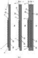
Figure 3 depicts schematics of a winding process, with adhesive movement filling a void space at the layer edge side, filling with adhesive tape, -
Figure 4 depicts schematics of the winding process, with adhesive movement filling the void space at the layer edge side, filling with dielectric string, -
Figure 5 depicts a winding where an adhesive has not reached a top area between wires, -
Figure 6 depicts a winding where an adhesive has reached a top area between wires, -
Figure 7 depicts a medium voltage transformer arrangement with a wrapped adhesive tape insulated primary coil module is presented, fitted with a dielectric shell, -
Figure 8 depicts a medium voltage transformer arrangement with a wrapped adhesive tape insulated primary coil module is presented, fitted with a conductive shell. - For a proper understanding of the disclosure, in the detailed description below corresponding elements or parts of the disclosure will be denoted with identical reference numerals in the drawings.
- The present invention discloses a method of winding a coil comprising steps of:
- a) winding a layer of a
wire 1 on aninsulation 2 other than epoxy resins such that the layer of thewire 1 immerses in an adhesive and pushes anexcess 5 adhesive towards both sides of thewire 1, - b) placing the layer of
insulation 2 on the layer of thewire 1, - In the present embodiment the layer of
insulation 2 is a tape with one or both sides coated with an adhesive comprising a carrier and adhesive layers. Thecarrier 2a is preferably a film, even more preferably is made of PET, PVC, PP, PEN, paper or paper composite.Adhesive layers 2b are preferably acrylic, silicone or rubber. In another embodiment the layer ofinsulation 2 is thermally activated adhesive tape. In this case during placing theinsulation 2, a heat is applied to theinsulation 2 before step b), after step b) or in different example of the invention - both. In another embodiment of the invention, the layer ofinsulation 2 is an adhesive tape which consists only of the adhesive layer. In this embodiment the layer ofinsulation 2 is a type of a transfer tape. - Winding the layer of the wire on the insulation results in immersing
wire 1 in the above-mentioned adhesive. The excess of adhesive is pushed towards both sides of thewire 1. In the case of winding a first layer of thewire 1, the excess adhesive is pushed towards both sides of thewire 1, where a first side is directed into an edge of the coil. In the case of multiply layers of thewire 1, the excess adhesive is also pushed towards another layer of thewire 1. Theadhesive layer 2b should completely fill any voids found between the layer of theinsulation 2 and thewire 1. That is of particular importance when considering the edge of the layers of the wire 1 - it is an area of high electric field and must be free of defects. - In different embodiment of the invention, after step a) a step c) is performed during which the rest, toward the at least one edge of the coil, of the layer of
insulation 2 on which the layer ofwire 1 is wound is filled such that the height of the coil, after step c), is approximately even. Preferably it is filled with anadditional insulation 2c or by winding adielectric string 7 with a diameter which matches the diameter of thewire 1. As the layer of thewire 1 is wound theexcess 5 adhesive forms a movement-a "wave", that travels in front of the layer of thewire 1. This movement,excess 5 adhesive, finally fills the potentially void space at the layer of thewire 1 edge, as it is shown inFig. 3 and4 . The adhesive makes the winding process very easy, since it fixes the layer of thewire 1 turns and prevents any sliding or misalignments. Thisexcess 5 adhesive can be in different embodiments any thermoplastic material. - There are several
adhesive layers 2b winding patterns possible, as shown in theFig. 2 . In other embodiment of the invention the layer ofinsulation 2 is placed during step b) such that it forms a layer structure - 2a on theFig. 2 , a brick wall structure - 2b on theFig. 2 , or an overlapped structure - 2c on theFig. 3 . For the simplicity of this disclosure all examples show the layer structure. - In different embodiment of the invention, before step b) a step d) is performed during which thin sheet of a
semiconductive tape 6 or a conductive, preferably metallic, tape or a wire is placed on the layer ofinsulation 2, on the at least one edge of the coil, such that the at least part of thesemiconductor tape 6 extends beyond the edge of the coil, wherein preferably thesemiconductive tape 6 is a semiconductive crepe paper or a semiconductive synthetic tape or a conductive, preferably metallic, tape or a wire. The parts of thesemiconductive tape 6 that extend beyond the edge of the coil can be connected galvanically together and grounded as it is shown inFig. 3 and4 . In this manner a groundedscreen 4 is formed around the coil, which can be used as a separate module. - In other embodiment of the invention wherein every next step a) is performed such that the layer of
wire 1 is shorter than the layer ofwire 1 wound during previous step a). The quality and dielectric strength of an adhesive interface between the edge of the layer of thewire 1 and the edge of the grounded tape forming the groundedscreen 4 is critical. Essentially, the bottom layers of thewire 1 are at lower potential than the top layers. Winding the coil in a trapezoidal fashion, with longer bottom layers with edges closer to the groundedscreen 4 and shorter top layers with edges further from the grounded screen, as shown inFig. 7 andFig. 8 can yield best results. - It is important that the adhesive film layers 2b are wound evenly, without any wrinkling where air could be trapped. To achieve this once a layer of the
wire 1 is finished, the rest of theadhesive layer 2b towards the edge should somehow be filled. It can be done by means of adding anadditional insulation 2c in the form of thin strip ofadhesive layer 2b as it is shown inFig. 3 , or by means of adding adielectric string 7, the diameter of which matches the diameter of thewire 1 as it is shown inFig. 4 . - In other embodiment of the invention before step a) a step e) is performed during which the layer of
insulation 2 is placed on abobbin 8 as it is seen onFig 6 and7 . - This invention also discloses a coil suitable for being used in transformers. It is needed that the layers of the
insulation 2 which come to the contact with a layer of awire 1 will ensure that all voids around thewires 1 are filled. This coil comprises at least one layer of thewire 1 and at least two layers of theinsulation 2. Thewire 1 ends with a terminal on each end, wherein the terminal is placed such that it may be connected to, and the layer of thewire 1 is placed between two of the at least two layers of theinsulation 2. The layer of thewire 1 is typically made from a copper, but it is known that thewire 1 can be made from any metal and alloys or that thewire 1 can be replaced with any conductor suitable for winding. - In the prior art, seen on
Fig. 1 , it is known to create coils consisting of layers of a wire PA2 and an insulation PA3. Firstly, the layers of the insulation PA3 are wrapped and then the layers of the wire PA2 are wrapped over the layer of the insulation PA3. The insulation PA3 is made from porous structure material. At the final stage, the coil is impregnated with epoxy resin PA1. Such coil alco comprises a screen PA4 and a core PA5. The present invention's coil doesn't require use of the epoxy resin which very often contains compounds having negative impact on the human health and environment and eliminates time consuming process of impregnation and curing. - In one of the embodiments the layer of
insulation 2 is a tape with one or both sides coated with an adhesive comprising acarrier 2a andadhesive layers 2b. Thecarrier 2a is preferably a film and even more preferably made of PET, PVC, PP, PEN, paper or paper composite.Adhesive layers 2b are preferably acrylic, silicone or rubber, or the insulation is thermally activated adhesive tape. The tape film must be ensured by high, defect free quality, ensuring high dielectric withstand. The thickness of the tape can be typically between 10 - 200 µm. A distance between the layers of thewire 1 is preferably 20-300µm. In another embodiment of the invention, the layer ofinsulation 2 is an adhesive tape which consists only of the adhesive layer. In this embodiment the layer ofinsulation 2 is a type of a transfer tape. - The adhesive thickness is in one of the embodiments between 10 - 150 µm, and it is best selected in such a way that it is optimized with regard to the diameter of the coil wire. In the best solution, the
adhesive layer 2b should completely fill any voids found between the layer of theinsulation 2 and thewire 1. That is of particular importance when considering the edge of the layers of thewire 1. In other embodiment of the invention the layer ofinsulation 2 on which the layer of thewire 1 is wound is filled toward the at least one edge of the coil such that the height of the layer of the wire is approximately even, preferably it is filled on the at least one edge with theadditional insulation 2c or with the layer of thedielectric string 7 with the diameter which matches the diameter of thewire 1. - In one embodiment of the invention, instead of the last layer of the
wire 1, a conductive/semiconductive screen is placed. - In different embodiment of the invention a thin sheet of a
semiconductive tape 6 or a conductive, preferably metallic, tape or a wire is placed on the at least one layer of theinsulation 2, on the at least one edge of the coil, such that the at least part of thesemiconductor tape 6 extends beyond the edge of the coil, wherein preferably thesemiconductive tape 6 is a semiconductive crepe paper or a semiconductive synthetic tape or a conductive, preferably metallic, tape or a wire. - As it is seen in
Fig. 3 and4 , layers of thewire 1 wrapped on the surface of theadhesive layer 2b with sufficient tension will push out the underlayingadhesive layer 2b to the free space between them. This results in immersion of thewires 1 in theadhesive layer 2b (glue) and elimination of voids between them. Then nextadhesive layer 2b covering thewires 1 from top (also applied with certain pressure) fills the remaining voids and finally the completely free structure consisting of the polymeric film wires -carriers 2a, andadhesive layer 2b is achieved. - It should be noted that in reality there is some free space between
wires 1 as shown inFig. 5 and 6 . During a winding process the adhesive is pushed toward edges as theexcess adhesive 5 of the current winding layer and towardadjacent wires 1. Usually also only the bottom area 1' between thewires 1 is filled with the adhesive however it is possible, due to the greater force used during the winding process or by means of greater amount of the adhesive used, that the adhesive will also fill thetop area 1" between thewires 1. In such cases it will be sufficient that thecarrier 2a will have only oneadhesive layer 2b since the adhesive will be able to insulateadjacent wires 1. - In other embodiment of the invention the coil comprises a
bobbin 8 near the portion of the coil which is closest to the center of the coil. - This invention also discloses a
transformer 10 comprising at least two coils and acore 3 placed inside of the at least two coils, where those coils are afirst coil 14 and asecond coil 15. Thefirst coil 14 and thesecond coil 15 are the coils according to the presented invention. - In different embodiment of the invention the
core 3 and the at least two coils, thefirst coil 14 and thesecond coil 15, are placed within adielectric shell 9 as it is shown inFig. 7 . Theshell 9 is preferably made from SMC, BMC or thermoplastic material. Material should have sufficient dielectric strength. - The
transformer 10 in different embodiment has amedium voltage screen 17 and abaseplate 16. - In different embodiment of the invention, having a
dielectric shell 9 requires adding an additionaldielectric material layer 11 to protect from a flashover between the terminal and thescreen 4 surrounding the coil formed from at least one thin sheet of a semiconductive tape placed on the at least one layer of theinsulation 2, on the at least one edge of the coil. Additionaldielectric material layer 11 is to prevent an internal breakdown from the medium voltage lead to the groundedscreen 4. The additionaldielectric material layer 11 can be room temperature cured silicone gel, polyurethane, or even silica filled epoxy. - The
transformer 10 is preferably placed, in one of the embodiments, within aconductive shell 13, preferably made of metal as it is shown inFig. 7 . Aconductive shell 13 renders thevoltage transformer 10 touch proof - no electric field is present on the surface of the apparatus. Such solutions are commonly used in GIS switchgears. Theshell 13 can be made from any conductive material, such as metal sheets. It can also be made from a dielectric material, coated with conductive paint or a layer of metallization. If theconductive shell 13 arrangement is considered, no additional secondary dielectric insulation is required. However, in other embodiment of the invention, the transformer comprises abushing 12. Thebushing 12 is needed to feed the medium voltage lead through the grounded shell. - Legend:
- 1- wire
- 1' - bottom area between wires
- 1" - top area between wires
- 2 - insulation
- 2a - carrier
- 2b - adhesive layer
- 2c - additional insulation
- 3 - core
- 4 - screen
- 5 - excess adhesive
- 6 - semiconductive tape
- 7 - string
- 8 - bobbin
- 9 - dielectric shell
- 10 - transformer
- 11 - additional dielectric material layer
- 12 - bushing
- 13 - conductive shell
- 14 - first coil
- 15 - second coil
- 16 - baseplate
- 17 - medium voltage screen
Claims (15)
- A method of winding a coil comprising steps of:a) Winding a layer of a wire (1) on an insulation (2) other than epoxy resins such that the layer of the wire (1) immerses in an adhesive and pushes an excess (5) adhesive towards both sides of the wire (1);b) Placing the layer of insulation (2) on the layer of the wire (1);wherein steps a) and b) are performed at least once.
- The method of winding a coil according to claim 1, wherein after step a) a step c) is performed during which the rest, toward the at least one edge of the coil, of the layer of insulation (2) on which the layer of wire (1) is wound is filled such that the height of the coil, after step c), is approximately even, preferably it is filled with an additional insulation (2c) or by winding a dielectric string (7) with a diameter which matches the diameter of the wire (1).
- The method of winding a coil according to claim 1 or 2, wherein before step b) a step d) is performed during which thin sheet of a semiconductive tape (6) or a conductive, preferably metallic, tape or a wire is placed on the layer of insulation (2), on the at least one edge of the coil, such that the at least part of the semiconductor tape (6) extends beyond the edge of the coil, wherein preferably the semiconductive tape (6) is a semiconductive crepe paper or a semiconductive synthetic tape or a conductive, preferably metallic, tape or a wire.
- The method of winding a coil according to anyone of claim 1-3, wherein the layer of insulation (2) is a tape with one or both sides coated with an adhesive comprisinga carrier (2a), preferably a film, even more preferably made of PET, PVC, PP, PEN, paper or paper composite,adhesive layers (2b), preferably acrylic, silicone or rubber, orthe layer of insulation (2) is a thermally activated adhesive tape and during placing of the insulation (2) a heat is applied to the insulation (2) before step b), after step b) or both, orthe layer of insulation (2) is an adhesive tape.
- The method of winding a coil according to anyone of claims 1-4, wherein the layer of insulation (2) is placed during step b) such that it forms a layer structure, a brick wall structure or an overlapped structure.
- A coil suitable for being used in transformers (10) comprising:at least one layer of a wire (1), wherein the wire (1) ends with a terminal on each end, whereinthe terminal is placed such that it may be connected to,at least two layers of an insulation (2), wherein the layer of the wire (1) is placed between two of the at least two layers of the insulation (2),wherein the layer of insulation (2) is a tape with one or both sides coated with an adhesive comprisinga carrier (2a), preferably a film, even more preferably made of PET, PVC, PP, PEN, paper or paper composite,adhesive layers (2b), preferably acrylic, silicone or rubber, orthe layer of insulation (2) is thermally activated adhesive tape, orthe layer of insulation (2) is an adhesive tape.
- The coil according to claim 6, wherein a thickness of the layer of the insulation (2) is 10-300 µm.
- The coil according to claim 6 or 7, wherein a distance between the layers of the wire (1) is 20-300 µm.
- The coil according to any one of claims 6-8 wherein the layer of insulation (2) on which the layer of the wire (1) is wound is filled toward the at least one edge of the coil such that the height of the layer of the wire (1) is approximately even, preferably it is filled on the at least one edge with an additional insulation (2c) or with a layer of a dielectric string (7) with a diameter which matches the diameter of the wire (1).
- The coil according to any one of claims 6-9 wherein a thin sheet of a semiconductive tape (6) or a conductive, preferably metallic, tape or a wire is placed on the at least one layer of the insulation, on the at least one edge of the coil, such that the at least part of the semiconductor tape (6) extends beyond the edge of the coil, wherein preferably the semiconductive tape (6) is a semiconductive crepe paper or a semiconductive synthetic tape or a conductive, preferably metallic, tape or a wire.
- The coil according to any one of claims6-10 wherein comprises a bobbin (8) near the portion of the coil which is closest to the center of the coil.
- A transformer (10) comprising a first coil (14), a second coil (15) and a core (3) placed inside of the at least two coils, wherein the first coil (14) is the coil according to claims 8-13, and preferably the second coil (15) is also the coil according to claims 8-13.
- The transformer (10) according to claim 12, wherein the core (3) and the at least two coils, the first coil (14) and the second coil (15), are placed within a dielectric shell (9), preferably made from SMC, BMC or thermoplastic material.
- The transformer (10) according to claim 12 or 13, wherein comprising an additional dielectric material layer (11) to protect from a flashover between the terminal and the screen (4) surrounding the coil formed from at least one thin sheet of a semiconductive tape placed on the at least one layer of the insulation (2), on the at least one edge of the coil.
- The transformer (10) according to any one of claims 12-14 wherein is placed within a conductive shell (13), preferably made of metal.
Priority Applications (1)
| Application Number | Priority Date | Filing Date | Title |
|---|---|---|---|
| EP23203573.3A EP4539066A1 (en) | 2023-10-13 | 2023-10-13 | Method of winding a coil, coil suitable for being used in transformers and transformer |
Applications Claiming Priority (1)
| Application Number | Priority Date | Filing Date | Title |
|---|---|---|---|
| EP23203573.3A EP4539066A1 (en) | 2023-10-13 | 2023-10-13 | Method of winding a coil, coil suitable for being used in transformers and transformer |
Publications (1)
| Publication Number | Publication Date |
|---|---|
| EP4539066A1 true EP4539066A1 (en) | 2025-04-16 |
Family
ID=88413363
Family Applications (1)
| Application Number | Title | Priority Date | Filing Date |
|---|---|---|---|
| EP23203573.3A Pending EP4539066A1 (en) | 2023-10-13 | 2023-10-13 | Method of winding a coil, coil suitable for being used in transformers and transformer |
Country Status (1)
| Country | Link |
|---|---|
| EP (1) | EP4539066A1 (en) |
Citations (6)
| Publication number | Priority date | Publication date | Assignee | Title |
|---|---|---|---|---|
| JPS5574956A (en) * | 1978-12-04 | 1980-06-05 | Mitsubishi Electric Corp | Winding method of electromagnetic coil |
| EP0171688A1 (en) * | 1984-08-04 | 1986-02-19 | Mwb Messwandler-Bau Ag | Method of manufacturing a sheet winding and sheet winding manufactured according to this method |
| JPH07326525A (en) * | 1994-05-31 | 1995-12-12 | Sumitomo 3M Ltd | Insulating adhesive tape and transformer using the same |
| US5767760A (en) * | 1995-12-21 | 1998-06-16 | Dow Corning S. A. | Foils |
| CN111613411A (en) * | 2019-02-25 | 2020-09-01 | 尤大千 | Insulation winding of electrical equipment using sintering process and ground shielding technology |
| EP3968345A1 (en) | 2020-09-11 | 2022-03-16 | ABB Schweiz AG | A primary coil and a method for manufacturing a primary coil |
-
2023
- 2023-10-13 EP EP23203573.3A patent/EP4539066A1/en active Pending
Patent Citations (6)
| Publication number | Priority date | Publication date | Assignee | Title |
|---|---|---|---|---|
| JPS5574956A (en) * | 1978-12-04 | 1980-06-05 | Mitsubishi Electric Corp | Winding method of electromagnetic coil |
| EP0171688A1 (en) * | 1984-08-04 | 1986-02-19 | Mwb Messwandler-Bau Ag | Method of manufacturing a sheet winding and sheet winding manufactured according to this method |
| JPH07326525A (en) * | 1994-05-31 | 1995-12-12 | Sumitomo 3M Ltd | Insulating adhesive tape and transformer using the same |
| US5767760A (en) * | 1995-12-21 | 1998-06-16 | Dow Corning S. A. | Foils |
| CN111613411A (en) * | 2019-02-25 | 2020-09-01 | 尤大千 | Insulation winding of electrical equipment using sintering process and ground shielding technology |
| EP3968345A1 (en) | 2020-09-11 | 2022-03-16 | ABB Schweiz AG | A primary coil and a method for manufacturing a primary coil |
Similar Documents
| Publication | Publication Date | Title |
|---|---|---|
| EP3103124B1 (en) | Condenser core | |
| US8154374B2 (en) | Transformer winding and a method of reinforcing a transformer winding | |
| EP2800112A1 (en) | HV instrument transformer | |
| AU2013361806B2 (en) | Transformer insulation | |
| US20230282411A1 (en) | Primary Coil and a Method for Manufacturing a Primary Coil | |
| US2246159A (en) | Electrical coil | |
| CN107925292B (en) | The stator and rotating electric machine of rotating electric machine | |
| EP3361481A1 (en) | Producing power bushing condenser core by additive manufacturing | |
| EP4539066A1 (en) | Method of winding a coil, coil suitable for being used in transformers and transformer | |
| US4751488A (en) | High voltage capability electrical coils insulated with materials containing SF6 gas | |
| CN100524550C (en) | Low voltage composite mold | |
| US20210035725A1 (en) | Transformer and method for manufacturing the same | |
| JPS5937660B2 (en) | Winding insulators for electrical machine coil windings | |
| CN111758139A (en) | Capacitive bushing, transformer and method for producing capacitive bushing | |
| US20240112849A1 (en) | Transformer Coil | |
| US3112357A (en) | Crack free insulated conductors and method of manufacture | |
| CN101313369B (en) | Mica reinforced insulation | |
| EP1953771A1 (en) | An electric insulation element, a bushing provided therewith, and a method of producing such an element | |
| JP2895679B2 (en) | Superconducting magnet | |
| KR102750401B1 (en) | Making method of bushing for condenser | |
| JP2009268274A (en) | Method of manufacturing coil for rotary electric machine and coil for rotary electric machine | |
| EP4369361A1 (en) | Compact high-voltage pulse transformer and method of manufacturing same | |
| JPH05152139A (en) | Insulating electric wire for high-frequency transformer, and high-frequency transformer itself using it | |
| JPH1092659A (en) | Gas insulated transformer | |
| JP2001327108A (en) | Stator coil of rotating electric machine |
Legal Events
| Date | Code | Title | Description |
|---|---|---|---|
| PUAI | Public reference made under article 153(3) epc to a published international application that has entered the european phase |
Free format text: ORIGINAL CODE: 0009012 |
|
| STAA | Information on the status of an ep patent application or granted ep patent |
Free format text: STATUS: THE APPLICATION HAS BEEN PUBLISHED |
|
| AK | Designated contracting states |
Kind code of ref document: A1 Designated state(s): AL AT BE BG CH CY CZ DE DK EE ES FI FR GB GR HR HU IE IS IT LI LT LU LV MC ME MK MT NL NO PL PT RO RS SE SI SK SM TR |
|
| STAA | Information on the status of an ep patent application or granted ep patent |
Free format text: STATUS: REQUEST FOR EXAMINATION WAS MADE |
|
| 17P | Request for examination filed |
Effective date: 20250827 |