EP4535967A1 - Wide bandgap perovskite - Google Patents
Wide bandgap perovskite Download PDFInfo
- Publication number
- EP4535967A1 EP4535967A1 EP23202239.2A EP23202239A EP4535967A1 EP 4535967 A1 EP4535967 A1 EP 4535967A1 EP 23202239 A EP23202239 A EP 23202239A EP 4535967 A1 EP4535967 A1 EP 4535967A1
- Authority
- EP
- European Patent Office
- Prior art keywords
- perovskite
- solution
- solvent
- preparing
- wide bandgap
- Prior art date
- Legal status (The legal status is an assumption and is not a legal conclusion. Google has not performed a legal analysis and makes no representation as to the accuracy of the status listed.)
- Pending
Links
- 238000000034 method Methods 0.000 claims abstract description 48
- 238000000151 deposition Methods 0.000 claims abstract description 30
- 239000000758 substrate Substances 0.000 claims abstract description 23
- 239000002904 solvent Substances 0.000 claims abstract description 22
- IAZDPXIOMUYVGZ-UHFFFAOYSA-N Dimethylsulphoxide Chemical compound CS(C)=O IAZDPXIOMUYVGZ-UHFFFAOYSA-N 0.000 claims abstract description 15
- 238000000137 annealing Methods 0.000 claims abstract description 8
- 239000012296 anti-solvent Substances 0.000 claims abstract description 8
- 238000002156 mixing Methods 0.000 claims abstract description 8
- RTZKZFJDLAIYFH-UHFFFAOYSA-N Diethyl ether Chemical group CCOCC RTZKZFJDLAIYFH-UHFFFAOYSA-N 0.000 claims description 30
- ZMXDDKWLCZADIW-UHFFFAOYSA-N N,N-dimethylformamide Substances CN(C)C=O ZMXDDKWLCZADIW-UHFFFAOYSA-N 0.000 claims description 12
- MVPPADPHJFYWMZ-UHFFFAOYSA-N chlorobenzene Chemical compound ClC1=CC=CC=C1 MVPPADPHJFYWMZ-UHFFFAOYSA-N 0.000 claims description 12
- YXFVVABEGXRONW-UHFFFAOYSA-N Toluene Chemical compound CC1=CC=CC=C1 YXFVVABEGXRONW-UHFFFAOYSA-N 0.000 claims description 9
- 239000000203 mixture Substances 0.000 claims description 4
- 150000001875 compounds Chemical class 0.000 claims description 3
- PEKFRNRSUCMVPD-UHFFFAOYSA-L [Pb](Cl)Cl.CN Chemical compound [Pb](Cl)Cl.CN PEKFRNRSUCMVPD-UHFFFAOYSA-L 0.000 claims description 2
- 239000010410 layer Substances 0.000 description 51
- 239000000463 material Substances 0.000 description 12
- 239000000075 oxide glass Substances 0.000 description 11
- 239000010408 film Substances 0.000 description 9
- 239000011521 glass Substances 0.000 description 8
- XOLBLPGZBRYERU-UHFFFAOYSA-N tin dioxide Chemical compound O=[Sn]=O XOLBLPGZBRYERU-UHFFFAOYSA-N 0.000 description 8
- 239000000523 sample Substances 0.000 description 7
- IJGRMHOSHXDMSA-UHFFFAOYSA-N Atomic nitrogen Chemical compound N#N IJGRMHOSHXDMSA-UHFFFAOYSA-N 0.000 description 6
- -1 99.9985%) Chemical compound 0.000 description 4
- QHJPGANWSLEMTI-UHFFFAOYSA-N aminomethylideneazanium;iodide Chemical compound I.NC=N QHJPGANWSLEMTI-UHFFFAOYSA-N 0.000 description 4
- XQPRBTXUXXVTKB-UHFFFAOYSA-M caesium iodide Inorganic materials [I-].[Cs+] XQPRBTXUXXVTKB-UHFFFAOYSA-M 0.000 description 4
- 230000000694 effects Effects 0.000 description 4
- RQQRAHKHDFPBMC-UHFFFAOYSA-L lead(ii) iodide Chemical compound I[Pb]I RQQRAHKHDFPBMC-UHFFFAOYSA-L 0.000 description 4
- WFUBYPSJBBQSOU-UHFFFAOYSA-M rubidium iodide Inorganic materials [Rb+].[I-] WFUBYPSJBBQSOU-UHFFFAOYSA-M 0.000 description 4
- 238000004528 spin coating Methods 0.000 description 4
- 238000009987 spinning Methods 0.000 description 4
- STTGYIUESPWXOW-UHFFFAOYSA-N 2,9-dimethyl-4,7-diphenyl-1,10-phenanthroline Chemical compound C=12C=CC3=C(C=4C=CC=CC=4)C=C(C)N=C3C2=NC(C)=CC=1C1=CC=CC=C1 STTGYIUESPWXOW-UHFFFAOYSA-N 0.000 description 3
- 229920000144 PEDOT:PSS Polymers 0.000 description 3
- 239000006096 absorbing agent Substances 0.000 description 3
- 238000006243 chemical reaction Methods 0.000 description 3
- ZASWJUOMEGBQCQ-UHFFFAOYSA-L dibromolead Chemical compound Br[Pb]Br ZASWJUOMEGBQCQ-UHFFFAOYSA-L 0.000 description 3
- 238000005516 engineering process Methods 0.000 description 3
- PJXISJQVUVHSOJ-UHFFFAOYSA-N indium(III) oxide Inorganic materials [O-2].[O-2].[O-2].[In+3].[In+3] PJXISJQVUVHSOJ-UHFFFAOYSA-N 0.000 description 3
- AMGQUBHHOARCQH-UHFFFAOYSA-N indium;oxotin Chemical compound [In].[Sn]=O AMGQUBHHOARCQH-UHFFFAOYSA-N 0.000 description 3
- HWSZZLVAJGOAAY-UHFFFAOYSA-L lead(II) chloride Chemical compound Cl[Pb]Cl HWSZZLVAJGOAAY-UHFFFAOYSA-L 0.000 description 3
- NQMRYBIKMRVZLB-UHFFFAOYSA-N methylamine hydrochloride Chemical compound [Cl-].[NH3+]C NQMRYBIKMRVZLB-UHFFFAOYSA-N 0.000 description 3
- LLWRXQXPJMPHLR-UHFFFAOYSA-N methylazanium;iodide Chemical compound [I-].[NH3+]C LLWRXQXPJMPHLR-UHFFFAOYSA-N 0.000 description 3
- 239000013545 self-assembled monolayer Substances 0.000 description 3
- 239000000126 substance Substances 0.000 description 3
- CSCPPACGZOOCGX-UHFFFAOYSA-N Acetone Chemical compound CC(C)=O CSCPPACGZOOCGX-UHFFFAOYSA-N 0.000 description 2
- LFQSCWFLJHTTHZ-UHFFFAOYSA-N Ethanol Chemical compound CCO LFQSCWFLJHTTHZ-UHFFFAOYSA-N 0.000 description 2
- YCKRFDGAMUMZLT-UHFFFAOYSA-N Fluorine atom Chemical compound [F] YCKRFDGAMUMZLT-UHFFFAOYSA-N 0.000 description 2
- KFZMGEQAYNKOFK-UHFFFAOYSA-N Isopropanol Chemical compound CC(C)O KFZMGEQAYNKOFK-UHFFFAOYSA-N 0.000 description 2
- XUIMIQQOPSSXEZ-UHFFFAOYSA-N Silicon Chemical compound [Si] XUIMIQQOPSSXEZ-UHFFFAOYSA-N 0.000 description 2
- KTSFMFGEAAANTF-UHFFFAOYSA-N [Cu].[Se].[Se].[In] Chemical compound [Cu].[Se].[Se].[In] KTSFMFGEAAANTF-UHFFFAOYSA-N 0.000 description 2
- 238000002835 absorbance Methods 0.000 description 2
- 230000001133 acceleration Effects 0.000 description 2
- LYQFWZFBNBDLEO-UHFFFAOYSA-M caesium bromide Chemical compound [Br-].[Cs+] LYQFWZFBNBDLEO-UHFFFAOYSA-M 0.000 description 2
- 150000001768 cations Chemical class 0.000 description 2
- 239000010949 copper Substances 0.000 description 2
- 230000008021 deposition Effects 0.000 description 2
- 229910052731 fluorine Inorganic materials 0.000 description 2
- 239000011737 fluorine Substances 0.000 description 2
- 238000001000 micrograph Methods 0.000 description 2
- 230000004048 modification Effects 0.000 description 2
- 238000012986 modification Methods 0.000 description 2
- 229910052757 nitrogen Inorganic materials 0.000 description 2
- 238000013082 photovoltaic technology Methods 0.000 description 2
- 239000002243 precursor Substances 0.000 description 2
- 238000002360 preparation method Methods 0.000 description 2
- 230000008569 process Effects 0.000 description 2
- 229910052710 silicon Inorganic materials 0.000 description 2
- 239000010703 silicon Substances 0.000 description 2
- 238000004544 sputter deposition Methods 0.000 description 2
- 239000010409 thin film Substances 0.000 description 2
- 229910001887 tin oxide Inorganic materials 0.000 description 2
- 229910052724 xenon Inorganic materials 0.000 description 2
- FHNFHKCVQCLJFQ-UHFFFAOYSA-N xenon atom Chemical compound [Xe] FHNFHKCVQCLJFQ-UHFFFAOYSA-N 0.000 description 2
- CPELXLSAUQHCOX-UHFFFAOYSA-M Bromide Chemical compound [Br-] CPELXLSAUQHCOX-UHFFFAOYSA-M 0.000 description 1
- RYGMFSIKBFXOCR-UHFFFAOYSA-N Copper Chemical compound [Cu] RYGMFSIKBFXOCR-UHFFFAOYSA-N 0.000 description 1
- IWNWLPUNKAYUAW-UHFFFAOYSA-N Ethylendiamine dihydroiodide Chemical compound I.I.NCCN IWNWLPUNKAYUAW-UHFFFAOYSA-N 0.000 description 1
- 241000272186 Falco columbarius Species 0.000 description 1
- CBENFWSGALASAD-UHFFFAOYSA-N Ozone Chemical compound [O-][O+]=O CBENFWSGALASAD-UHFFFAOYSA-N 0.000 description 1
- 229910020220 Pb—Sn Inorganic materials 0.000 description 1
- 229920001609 Poly(3,4-ethylenedioxythiophene) Polymers 0.000 description 1
- BQCADISMDOOEFD-UHFFFAOYSA-N Silver Chemical compound [Ag] BQCADISMDOOEFD-UHFFFAOYSA-N 0.000 description 1
- 229910020816 Sn Pb Inorganic materials 0.000 description 1
- 229910020922 Sn-Pb Inorganic materials 0.000 description 1
- 229910008783 Sn—Pb Inorganic materials 0.000 description 1
- 238000000862 absorption spectrum Methods 0.000 description 1
- 238000005275 alloying Methods 0.000 description 1
- 230000015572 biosynthetic process Effects 0.000 description 1
- 150000001767 cationic compounds Chemical class 0.000 description 1
- 230000008859 change Effects 0.000 description 1
- 238000004140 cleaning Methods 0.000 description 1
- 229910052802 copper Inorganic materials 0.000 description 1
- 239000013078 crystal Substances 0.000 description 1
- 230000006735 deficit Effects 0.000 description 1
- 238000004090 dissolution Methods 0.000 description 1
- 230000005611 electricity Effects 0.000 description 1
- 238000000295 emission spectrum Methods 0.000 description 1
- 230000005284 excitation Effects 0.000 description 1
- 238000000605 extraction Methods 0.000 description 1
- 150000004820 halides Chemical class 0.000 description 1
- XMBWDFGMSWQBCA-UHFFFAOYSA-N hydrogen iodide Chemical compound I XMBWDFGMSWQBCA-UHFFFAOYSA-N 0.000 description 1
- 238000005286 illumination Methods 0.000 description 1
- 229910001411 inorganic cation Inorganic materials 0.000 description 1
- 238000004519 manufacturing process Methods 0.000 description 1
- 238000005259 measurement Methods 0.000 description 1
- 229910001507 metal halide Inorganic materials 0.000 description 1
- 150000005309 metal halides Chemical class 0.000 description 1
- ISWNAMNOYHCTSB-UHFFFAOYSA-N methanamine;hydrobromide Chemical compound [Br-].[NH3+]C ISWNAMNOYHCTSB-UHFFFAOYSA-N 0.000 description 1
- WHXTVQNIFGXMSB-UHFFFAOYSA-N n-methyl-n-[tris(dimethylamino)stannyl]methanamine Chemical compound CN(C)[Sn](N(C)C)(N(C)C)N(C)C WHXTVQNIFGXMSB-UHFFFAOYSA-N 0.000 description 1
- 230000005693 optoelectronics Effects 0.000 description 1
- 150000002892 organic cations Chemical class 0.000 description 1
- 230000003647 oxidation Effects 0.000 description 1
- 238000007254 oxidation reaction Methods 0.000 description 1
- 229920001467 poly(styrenesulfonates) Polymers 0.000 description 1
- 229960002796 polystyrene sulfonate Drugs 0.000 description 1
- 239000011970 polystyrene sulfonate Substances 0.000 description 1
- 238000012545 processing Methods 0.000 description 1
- 238000011160 research Methods 0.000 description 1
- 238000005204 segregation Methods 0.000 description 1
- 239000002094 self assembled monolayer Substances 0.000 description 1
- 229910052709 silver Inorganic materials 0.000 description 1
- 239000004332 silver Substances 0.000 description 1
- 238000001228 spectrum Methods 0.000 description 1
- 238000003949 trap density measurement Methods 0.000 description 1
- 238000001771 vacuum deposition Methods 0.000 description 1
- 238000005406 washing Methods 0.000 description 1
Images

Classifications
-
- H—ELECTRICITY
- H10—SEMICONDUCTOR DEVICES; ELECTRIC SOLID-STATE DEVICES NOT OTHERWISE PROVIDED FOR
- H10K—ORGANIC ELECTRIC SOLID-STATE DEVICES
- H10K85/00—Organic materials used in the body or electrodes of devices covered by this subclass
- H10K85/50—Organic perovskites; Hybrid organic-inorganic perovskites [HOIP], e.g. CH3NH3PbI3
-
- H—ELECTRICITY
- H10—SEMICONDUCTOR DEVICES; ELECTRIC SOLID-STATE DEVICES NOT OTHERWISE PROVIDED FOR
- H10K—ORGANIC ELECTRIC SOLID-STATE DEVICES
- H10K30/00—Organic devices sensitive to infrared radiation, light, electromagnetic radiation of shorter wavelength or corpuscular radiation
- H10K30/50—Photovoltaic [PV] devices
- H10K30/57—Photovoltaic [PV] devices comprising multiple junctions, e.g. tandem PV cells
-
- H—ELECTRICITY
- H10—SEMICONDUCTOR DEVICES; ELECTRIC SOLID-STATE DEVICES NOT OTHERWISE PROVIDED FOR
- H10K—ORGANIC ELECTRIC SOLID-STATE DEVICES
- H10K71/00—Manufacture or treatment specially adapted for the organic devices covered by this subclass
- H10K71/10—Deposition of organic active material
- H10K71/12—Deposition of organic active material using liquid deposition, e.g. spin coating
-
- H—ELECTRICITY
- H10—SEMICONDUCTOR DEVICES; ELECTRIC SOLID-STATE DEVICES NOT OTHERWISE PROVIDED FOR
- H10K—ORGANIC ELECTRIC SOLID-STATE DEVICES
- H10K71/00—Manufacture or treatment specially adapted for the organic devices covered by this subclass
- H10K71/10—Deposition of organic active material
- H10K71/12—Deposition of organic active material using liquid deposition, e.g. spin coating
- H10K71/15—Deposition of organic active material using liquid deposition, e.g. spin coating characterised by the solvent used
-
- H—ELECTRICITY
- H10—SEMICONDUCTOR DEVICES; ELECTRIC SOLID-STATE DEVICES NOT OTHERWISE PROVIDED FOR
- H10K—ORGANIC ELECTRIC SOLID-STATE DEVICES
- H10K71/00—Manufacture or treatment specially adapted for the organic devices covered by this subclass
- H10K71/40—Thermal treatment, e.g. annealing in the presence of a solvent vapour
-
- Y—GENERAL TAGGING OF NEW TECHNOLOGICAL DEVELOPMENTS; GENERAL TAGGING OF CROSS-SECTIONAL TECHNOLOGIES SPANNING OVER SEVERAL SECTIONS OF THE IPC; TECHNICAL SUBJECTS COVERED BY FORMER USPC CROSS-REFERENCE ART COLLECTIONS [XRACs] AND DIGESTS
- Y02—TECHNOLOGIES OR APPLICATIONS FOR MITIGATION OR ADAPTATION AGAINST CLIMATE CHANGE
- Y02E—REDUCTION OF GREENHOUSE GAS [GHG] EMISSIONS, RELATED TO ENERGY GENERATION, TRANSMISSION OR DISTRIBUTION
- Y02E10/00—Energy generation through renewable energy sources
- Y02E10/50—Photovoltaic [PV] energy
- Y02E10/549—Organic PV cells
Definitions
- the invention notably relates to a method for making a wide bandgap perovskite for solar cell, an associated wide bandgap perovskite and a perovskite tandem device for solar cell comprising this wide bandgap perovskite.
- Metal Halide perovskite solar cells have recently emerged as high-efficiency and low-cost thin-film photovoltaic technology with 25.7% power conversion efficiency (PCE).
- PCE power conversion efficiency
- the high-power conversion efficiencies and stabilities over 1000 hours at 85°C under 1 Sun illumination have been obtained using lab scale processes and small cell areas.
- the building blocks of the perovskite materials are very low cost, and the processing into the final perovskite can be achieved with low-temperature fast processes. This makes these materials cost-efficient, enabling the potential to achieve a levelised cost of electricity (LCOE) estimated in different locations and the values range from 0.03 to 0.05 $/kWh, below that of today's mainstream photovoltaic (PV) technologies.
- LCOE levelised cost of electricity
- Metal halide perovskite absorbers consist of an ABX 3 formula.
- narrow-bandgap perovskites are prepared by Sn-Pb hybrids, which have a bandgap of about 1.25 eV, could be perfectly matched with the easily prepared wide-bandgap perovskite of 1.78 eV
- the narrow bandgap device of Pb-Sn is not stable due to Sn 2+ oxidation to Sn 4+ .
- the optimal wide bandgap (WBG) perovskites should have bandgap at about 1.86 eV to pair with low bandgap perovskites ( ⁇ 1.46 eV) in Pb/Pb perovskite tandems so that they can reach the theoretical maximum power conversion efficiency (PCE), which needs to be mixed with more Br - .
- PCE theoretical maximum power conversion efficiency
- 30% Br content is the limit to maintain stability (the bandgap is about 1.8 eV). If this value is exceeded, the stability and efficiency of WBG perovskite solar cells (PSCs) are constrained by the light-induced halide segregation resulting in the large photovoltage deficit.
- the present disclosure relates to a method for making a wide bandgap perovskite for solar cell, the method including:
- the method allows for preparing a high-quality and photostable WBG perovskites (1.85 eV) suitable for Pb/Pb perovskite tandems.
- perovskite gradually change from three-dimensional (3D) to two-dimensional (2D), which is more stable.
- Two-dimensional perovskite is obtained by compensating the large cations with Cs - to maintain a consistent average tolerance factor.
- the local distortions in the lattice parameters allowing increase of the lattice micro-strain and modification of the optoelectronic properties of the perovskite.
- the selection of values for y, A and B is the result of a comprehensive compromise between the band gap and crystal structure of the finished perovskite, which together determine the efficiency of the device.
- the stability of the device as a whole is greatly improved due to the more stable wide bandgap perovskite first exposure to harmful light and heat.
- the stable and high-efficiency WBG perovskite may be incorporated in perovskite/silicon 2-terminal and 4-terminal configurations.
- CIGS Copper Indium Gallium Selenide
- 10 ⁇ B ⁇ 20, for example B 15.
- the anti-solvent allows removing DMF and DMSO during the preparation process of the wide bandgap perovskite.
- the anti-solvent may be chosen among: diethyl ether, chlorobenzene, toluene, or a mixture of these compounds. Diethyl ether has the best effect.
- the present disclosure also relates to a wide bandgap perovskite for solar cell including IH 3 NCH 2 CH 2 NH 3 I at content between 10 and 20 mol%.
- This wide bandgap perovskite can be obtained by carrying the above described method.
- the present disclosure also relates to a method for fabricating a perovskite tandem device for solar cell, wherein the wide band gap perovskite is obtained by the above-described method.
- the method for fabricating the perovskite tandem device includes:
- the narrow bandgap perovskite layer has a bandgap lying in the range 1.46 eV to 1.59 eV.
- the present disclosure also relates to a perovskite tandem device including the above-described wide bandgap perovskite.
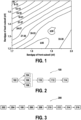
- the bandgap of mixed-cation mixed-halide lead perovskites can be tuned between 1.2 and 2.0 eV by varying the type and content of ABX 3 , which providing the possibility for the fabrication of tandem devices by perovskite/perovskite.
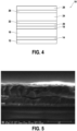
- FIG.2 shows a flow chart of a method 100 for making a wide bandgap perovskite for solar cell.
- the method 100 includes a step of preparing a solvent 102 by mixing 4 volumes of DMF and 1 volume of DMSO.
- the method 100 includes a step of preparing a first solution 104 of AM Cs 0.3 FA 0.7 Pb(I (1-y) Br y ) 3 with the solvent, wherein 1.00 ⁇ A ⁇ 1.55, for example 1.15 ⁇ A ⁇ 1.25, and 0.2 ⁇ y ⁇ 0.4, for example 0.25 ⁇ y ⁇ 0.35.
- the method 100 includes a step of preparing a second solution 106 of A M IH 3 NCH 2 CH 2 NH 3 Pbl 3 with the solvent.
- the method 100 includes a step of preparing a third solution 108 of AM MAPbCl 3 with the solvent.
- the method 100 includes a step of preparing a fourth solution 110 with 0.97*(100-B) vol% of the first solution, 0.97*B vol% of the second solution and 3 vol% of the third solution, wherein 2 ⁇ B ⁇ 22, for example 10 ⁇ B ⁇ 20.
- the method 100 includes a step of depositing a film 112 of the fourth solution on a substrate with diethyl ether, chlorobenzene, toluene, or a mixture of these compounds.
- the method 100 includes a step of annealing the deposited film 114 in inert atmosphere at temperature below 110°C to obtain the wide bandgap perovskite.
- the annealing step may comprise applying a first temperature lying in the range 55°C to 75°C during a first duration lying in the range 2 minutes to 4 minutes, and then applying a second temperature lying in the range 90°C to 105°C during a second duration lying in the range 10 minutes to 15 minutes.
- the step of preparing the first solution 104 of 1.2 M Cs 0.3 FA 0.7 Pb(I (1-y) Br y ) 3 with the solvent may be carried out by mixing 0.36 mmol CsBr, 0.36 mmol PbBr 2 , 0.84 mmol FAI and 0.84 mmol PbI 2 into 1 ml solvent.
- the step of preparing the second solution 106 of 1.2 M IH 3 NCH 2 CH 2 NH 3 PbI 3 with the solvent may be carried out by mixing 1.2 mmol IH 3 NCH 2 CH 2 NH 3 I and 1.2 mmol PbI 2 into 1 ml solvent.
- the step of preparing the third solution 108 may be carried out by mixing 1.2 mmol MACl and 1.2 mmol PbCl 2 into 1 ml solvent.
- the step of preparing the fourth solution 110 may be carried out by mixing 0.97*85 vol% of the first solution, 0.97*15 vol% of the second solution and 3 vol% of the third solution.
- the first and second solutions may first be mixed together and the third solution may then be added to the mix of the first and the second solutions.
- the step of depositing a film 112 of the fourth solution on a substrate with diethyl ether may be carried out by spin-coating, for example at 5000 rpm for 60 s with 750 ⁇ L diethyl ether dripped at 25 s during the spinning.
- FIG. 3 shows a flow chart of a method 200 for fabricating a perovskite tandem device for solar cell including a wide bandgap perovskite obtained by the method 100 for making a wide bandgap perovskite for solar cell described above and FIGS. 4 and 5 respectively show a schematic representation of a tandem device for solar cell and a micrograph of a tandem device for solar cell fabricated by the method 200 for fabricating a perovskite tandem device for solar cell. It is to be noted that FIG. 4 is not to scale.
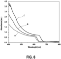
- FIG. 6 shows a graph of the absorbance in arbitrary unit as a function of the wavelength in nm
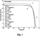
- FIG. 7 shows a graph of the current density in mA.cm -2 as a function of the voltage in V. Both graphs show the effect of both IH 3 NCH 2 CH 2 NH 3 I and Cl - into the mixed-cation mixed-halide perovskite.
- the curves labelled "A” correspond to the non-limiting example of the invention described above
- the curves labelled “B” are outside the scope of the invention and correspond to this non-limiting example wherein the third solution has been omitted (only first and second solutions)
- the curves labelled "C” are outside the scope of the invention and correspond to the use of the first and third solutions only (second solution omitted).
- the method 200 includes known-steps for making a tandem device 10.
- the method 200 includes a step 202 of preparing a patterned transparent conducting oxide glass substrate 12.
- the patterned transparent conducting oxide glass substrate 12 may be made of a glass substrate coated with indium tin oxide (ITO) or fluorine doped tin oxide (FTO).
- ITO indium tin oxide
- FTO fluorine doped tin oxide
- the method 200 includes a step 204 of depositing a first hole transporting material (HTM) layer 14 on the prepared patterned transparent conducting oxide glass substrate 12.
- HTM hole transporting material
- the method 200 includes a step of depositing a wide bandgap perovskite layer 16 by the above-described method 100 on the first hole transporting material layer 14.
- the method 200 includes a step 206 of depositing a first electron transport layer (ETL) 18 on the wide bandgap perovskite layer 16.
- ETL electron transport layer
- the method 200 includes a step 208 of depositing a transparent conducting oxide glass layer 20 on the first electron transport layer 18.
- the method 200 includes a step 210 of depositing a second hole transporting material (HTM) layer 22 on the transparent conducting oxide glass layer 20.
- HTM hole transporting material
- the method 200 includes a step 212 of depositing a narrow bandgap perovskite layer 24 on the second hole transporting material layer 22.
- the method 200 includes a step 214 of depositing a second electron transport layer 26 on the narrow bandgap perovskite layer 24.
- the method 200 includes a step 216 of depositing a counter electrode 28 on the second electron transport layer 26.
- Patterned transparent conducting oxide glass substrate In 2 O 3 /SnO 2 90/10 wt% on a glass substrate.
- MeO-2PACZ forming self-assembled monolayers (SAM) which form uniform coverage on top of oxide surface providing efficient extraction of positive charges.
- Wide bandgap perovskite layer 1.85 eV perovskite obtained by method 100.
- First electron transport layer C 60 .
- Transparent conducting oxide glass layer In 2 O 3 /SnO 2 90/10 wt%.
- Second hole transporting material layer PEDOT:PSS.
- Narrow bandgap perovskite layer 1.47 eV 1.5 M Rb 0.05 Cs 0.05 MA 0.05 FA 0.85 Pb(I 0.95 Br 0.05 ) 3 .
- Second electron transport layer C 60 .
- the step 202 of preparing the patterned transparent ITO glass substrate may be carried out by washing the ITO glass substrate with acetone and isopropanol for 15 min each.
- This substrate may correspond to commercial ITO glass that has been laser etched.
- the step 204 of depositing the first HTM layer on the prepared ITO substrate may be carried out by treating with ultraviolet ozone for 15 min the prepared ITO substrate and by spin-coating a 0.5 mg/ml MeO-2PACZ self-assembled monolayer solution dissolved in ethanol on the prepared ITO substrate at 3000 rpm for 30 s in a nitrogen glovebox. The spin-coated film was then annealed at 100°C for 10 min.
- the step of depositing the wide bandgap perovskite layer may be carried out by the above-described method 100 on the first HTM layer.
- the fourth solution may be deposited on the first HTM layer with diethyl ether by spin-coating, for example at 5000 rpm for 60 s with 750 ⁇ L diethyl ether dripped at 25 s during the spinning.
- the deposited film may be annealed in inert atmosphere at temperature below 110°C to obtain the wide bandgap perovskite.
- the annealing step may be carried out at 65°C for 2 min and then 100°C for 10 minutes in nitrogen (N 2 ).
- the step 206 of depositing the first ETL on the wide bandgap perovskite layer may be carried out by transferring the sample to an Angstrom evaporator for LiF (1 nm)/C 60 (30 nm) deposition.
- the transparent conducting oxide layer may be deposited onto the first ETL (step 208) by transferring the sample to a sputtering system and sputtering about 120 nm of ITO layer having a sheet resistance of around 30 ⁇ sq -1 from a 3 inch target at 100 W power under Ar pressure of 1.5 mtorr.
- the sheet resistance of the ITO layer was measured by using four-point probe method while the ITO layer was deposited on a glass substrate.
- the step 210 of depositing a second HTM layer on the transparent conducting oxide glass layer may be carried out by spin-coating a solution of PEDOT:PSS at 3000 rpm for 30 s in a nitrogen glovebox and post-annealing the spin-coated solution at 110°C for 5 min.
- the step 212 of depositing a narrow bandgap perovskite layer on the second HTM layer may be carried out by preparing a 1.5 M Rb 0.05 Cs 0.05 MA 0.05 FA 0.85 Pb(I 0.95 Br 0.05 ) 3 precursor solution in the solvent, the respective chemical molar ratio of CsI, RbI, FAI, PbI 2 , PbBr 2 and MABr being 0.05, 0.05, 0.85, 0.95, 0.05 and 0.05.
- the precursor solution was spin-coated onto the sample, the sample first spinning at 1000 rpm (within 1 s from 0 to 1000; no slow acceleration step) for 10 s, and then at 3000 rpm (no slow acceleration) for 40 s. After 15 s into the second stage (3000 rpm, 40 s), 150 ⁇ L of chlorobenzene antisolvent was dropped on top of the spinning sample. The perovskite layer was subsequently annealed at 100°C for 10 min.
- the step 214 of depositing the second ETL on the narrow bandgap perovskite layer may be carried out by transferring the sample to an Angstrom evaporator for LiF (1 nm)/C 60 (30 nm)/BCP (6 nm)/Ag (100 nm) deposition.
- the step 216 of depositing the copper counter electrode on the second electron transport layer may be carried out by vacuum evaporation method.
- Methylammonium iodide (MAI), methylammonium bromide (MAI), methylammonium chloride (MACl), ethane-1,2-diammonium iodide (IH 3 NCH 2 CH 2 NH 3 I) and formamidinium iodide (FAI) were purchased from the GreatCell Solar Company. Lead bromide (99.999%) and MeO-2PACZ was purchased from Tokyo Chemical Industry Co.
- Lead iodide (PbI 2 , 99.9985%), Rubidium iodide (RbI, 99.9%), caesium iodide (CsI, 99.9%) and diethyl ether were purchased from Alfa Aesar., N,N-dimethylmethanamide (DMF) (anhydrous), Lead chloride (PbCl 2 ), dimethyl sulfoxide (DMSO) (anhydrous), tetrakis(dimethylamino) tin (iv) (99.9999%) and chlorobenzene (CB) were purchased from Aldrich Sigma.
- Poly(3,4-ethylenedioxythiophene):polystyrene sulfonate (PEDOT:PSS, CLEVIOS P VP AI 4083) was purchased from Heraeus, LLC. Bathocuproine (BCP) were purchased from Jilin OLED Company (China). Indium tin oxide (ITO, In 2 O 3 /SnO 2 90/10 wt%) target and silver (Ag) were purchased from Kurt J. Lesker Company. All chemicals used in this work were commercially available and were used as received.
- FIG. 8 shows a graph of the External Quantum Efficiency (in %) as a function of the wavelength (in nm) for the wide bandgap perovskite (plain circles, curve “D") and the narrow bandgap perovskite (plain squares, curve “E") of the non-limiting example
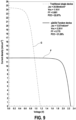
- FIG. 9 shows a graph of the current density (in mA.cm -2 ) as a function of the voltage (in V) for the tandem device of the non-limiting example (curve "F”) compared to a traditional single device (curve "G”).
- the single junction solar cells exhibit 1.0 to 1.2 V open circuit potential.
- the tandem device shows double the voltage of single junction solar cell.
- the tandem device exhibited the characteristic of doubling the voltage and halving the current, with a fill factor (FF) of 0.775, and showed a consistent PCE (21.28%).
- adding more Br should make the perovskite absorber more stable, given the strength of the lead (Pb)-Br bond relative to the Pb-I bond.
- the wide bandgap perovskite that is first exposed to harmful factors such as UV and heat can better protect the narrow bandgap perovskite bottom cell, thereby improving the overall stability of 2T tandem devices
- IPCE spectra were recorded as functions of wavelength under a constant white light bias of ⁇ 10 mW ⁇ cm -2 supplied by an array of white light emitting diodes.
- the excitation beam coming from a 300 W xenon lamp (ILC Technology) was focused through a Gemini-180 double monochromator (Jobin Yvon Ltd) and chopped at ⁇ 2 Hz.
- the signal was recorded using a Model SR830 DSP Lock-In Amplifier (Stanford Research Systems).
Landscapes
- Engineering & Computer Science (AREA)
- Chemical & Material Sciences (AREA)
- Materials Engineering (AREA)
- Manufacturing & Machinery (AREA)
- Physics & Mathematics (AREA)
- Electromagnetism (AREA)
- Photovoltaic Devices (AREA)
Abstract
A method for making a wide bandgap perovskite includes: preparing a solvent (102) by mixing 4 volumes of DMF and 1 volume of DMSO; preparing a first solution (104) of AM Cs0.3FA0.7Pb(I(1-y)Bry)3 with the solvent; preparing a second solution (106) of AM IH3NCH2CH2NH3PbI3 with the solvent; preparing a third solution (108) of AM MAPbCl3 with the solvent; preparing a fourth solution (110) with 0.97∗(100-B) vol% of the first solution, 0.97*B vol% of the second solution and 3 vol% of the third solution, wherein 2 ≤ B ≤ 22; depositing a film (112) of the fourth solution on a substrate with an anti-solvent; annealing the deposited film (114) in inert atmosphere at temperature below 110°C to obtain the wide bandgap perovskite.
Description
- The invention notably relates to a method for making a wide bandgap perovskite for solar cell, an associated wide bandgap perovskite and a perovskite tandem device for solar cell comprising this wide bandgap perovskite.
- Metal Halide perovskite solar cells have recently emerged as high-efficiency and low-cost thin-film photovoltaic technology with 25.7% power conversion efficiency (PCE). The high-power conversion efficiencies and stabilities over 1000 hours at 85°C under 1 Sun illumination have been obtained using lab scale processes and small cell areas. The building blocks of the perovskite materials are very low cost, and the processing into the final perovskite can be achieved with low-temperature fast processes. This makes these materials cost-efficient, enabling the potential to achieve a levelised cost of electricity (LCOE) estimated in different locations and the values range from 0.03 to 0.05 $/kWh, below that of today's mainstream photovoltaic (PV) technologies.
- Although these achievements are impressive, the use of more stable structure towards solar cells commercially available still needs to be demonstrated to make perovskite solar cells a real alternative to the existing Si-based technology.
- Metal halide perovskite absorbers consist of an ABX3 formula. The B-cation is coordinated octahedrally by X-anions, and the A-cation fills the cuboctahedral voids and compensates for the negative charge, where X generally is Cl, Br, or I, the A-site is either inorganic cation Cs+ or organic cations, such as CH3NH3 + (MA) and NH2CH=NH2 + (FA), the B-site is either Pb2+ or Sn2+ (or a combination of them).
- Typically, for perovskite/perovskite tandem devices, narrow-bandgap perovskites are prepared by Sn-Pb hybrids, which have a bandgap of about 1.25 eV, could be perfectly matched with the easily prepared wide-bandgap perovskite of 1.78 eV
- However, the narrow bandgap device of Pb-Sn is not stable due to Sn2+ oxidation to Sn4+.
- Therefore, for narrow bandgap it is better to use stable pure lead perovskites.
- But the difficulty is that the optimal wide bandgap (WBG) perovskites should have bandgap at about 1.86 eV to pair with low bandgap perovskites (≈1.46 eV) in Pb/Pb perovskite tandems so that they can reach the theoretical maximum power conversion efficiency (PCE), which needs to be mixed with more Br-. However, usually, 30% Br content is the limit to maintain stability (the bandgap is about 1.8 eV). If this value is exceeded, the stability and efficiency of WBG perovskite solar cells (PSCs) are constrained by the light-induced halide segregation resulting in the large photovoltage deficit.
- The present disclosure relates to a method for making a wide bandgap perovskite for solar cell, the method including:
- preparing a solvent by mixing 4 volumes of DMF (dimethylformamide) and 1 volume of DMSO (dimethyl sulfoxide);
- preparing a first solution of AM Cs0.3FA0.7Pb(I(1-y)Bry)3 with the solvent, wherein FA designates NH2CH=NH2 + and wherein 1.00 ≤ A ≤ 1.55 and 0.2 ≤ y ≤ 0.4;
- preparing a second solution of A M IH3NCH2CH2NH3PbI3 with the solvent;
- preparing a third solution of A M methylammonium lead chloride noted MAPbCl3 with the solvent;
- preparing a fourth solution with 0.97*(100-B) vol% of the first solution, 0.97*B vol% of the second solution and the additional 3 vol% of the third solution, wherein 2 ≤ B ≤ 22;
- depositing a film of the fourth solution on a substrate with an anti-solvent; and
- annealing the deposited film in inert atmosphere at temperature below 110°C to obtain the wide bandgap perovskite.
- The method allows for preparing a high-quality and photostable WBG perovskites (1.85 eV) suitable for Pb/Pb perovskite tandems.
- By alloying IH3NCH2CH2NH3I and Cl- into the mixed-cation mixed-halide perovskites, a wide bandgap perovskite absorber is obtained with lower bromide contents while the lattice strain and trap densities are simultaneously minimized.
- Moreover, the dissolution of large cations makes the properties of perovskite gradually change from three-dimensional (3D) to two-dimensional (2D), which is more stable. Two-dimensional perovskite is obtained by compensating the large cations with Cs- to maintain a consistent average tolerance factor. The local distortions in the lattice parameters allowing increase of the lattice micro-strain and modification of the optoelectronic properties of the perovskite. The selection of values for y, A and B is the result of a comprehensive compromise between the band gap and crystal structure of the finished perovskite, which together determine the efficiency of the device.
- After assembly into a tandem, the stability of the device as a whole is greatly improved due to the more stable wide bandgap perovskite first exposure to harmful light and heat.
- In addition, the stable and high-efficiency WBG perovskite may be incorporated in perovskite/silicon 2-terminal and 4-terminal configurations.
- Also, another high-efficiency thin film technology CIGS (Copper Indium Gallium Selenide) may be used to replace silicon bottom cells.
- In some embodiments, 0.25 ≤ y ≤ 0.35, for example y = 0.3.
- In some embodiments, 1.15 ≤ A ≤ 1.25, for example A = 1.20.
- In some embodiments, 10 ≤ B ≤ 20, for example B = 15.
- The anti-solvent allows removing DMF and DMSO during the preparation process of the wide bandgap perovskite. The anti-solvent may be chosen among: diethyl ether, chlorobenzene, toluene, or a mixture of these compounds. Diethyl ether has the best effect.
- The present disclosure also relates to a wide bandgap perovskite for solar cell including IH3NCH2CH2NH3I at content between 10 and 20 mol%. This wide bandgap perovskite can be obtained by carrying the above described method.
- The present disclosure also relates to a method for fabricating a perovskite tandem device for solar cell, wherein the wide band gap perovskite is obtained by the above-described method.
- The method for fabricating the perovskite tandem device includes:
- preparing a patterned transparent conducting oxide glass substrate, e.g. a transparent conducting ITO (indium tin oxide) glass substrate or a transparent conducting FTO (fluorine doped tin oxide) glass substrate; this preparation step may comprise a cleaning of the patterned transparent conducting oxide glass substrate;
- depositing a first hole transporting material layer on the prepared patterned transparent conducting oxide glass substrate;
- depositing the wide bandgap perovskite layer by the above-described method on the first hole transporting material layer;
- depositing a first electron transport layer on the wide bandgap perovskite layer;
- depositing a transparent ITO layer on the first electron transport layer;
- depositing a second hole transporting material layer on the transparent ITO layer;
- depositing a narrow bandgap perovskite layer on the second hole transporting material layer;
- depositing a second electron transport layer on the narrow bandgap perovskite layer;
- depositing a counter electrode on the second electron transport layer.
- The narrow bandgap perovskite layer has a bandgap lying in the range 1.46 eV to 1.59 eV.
- The present disclosure also relates to a perovskite tandem device including the above-described wide bandgap perovskite.
- Features, advantages, and technical and industrial significance of exemplary embodiments of the invention will be described below with reference to the accompanying drawings, in which like signs denote like elements, and wherein:
-
FIG. 1 shows the PCE as a function of the bandgap of the front subcell and the back subcell in a tandem device; -
FIG. 2 shows a flow chart of a method for making a wide bandgap perovskite for solar cell according to an embodiment of the invention; -
FIG. 3 shows a flow chart of a method for fabricating a perovskite tandem device for solar cell according to an embodiment of the invention; -
FIG. 4 shows a schematic representation of a tandem device for solar cell according to an embodiment of the invention; -
FIG. 5 shows a micrograph of a tandem device for solar cell according to the non-limiting example described below; -
FIG. 6 shows a graph of the absorbance (in arbitrary units) as a function of the wavelength (in nm) showing the effect of both IH3NCH2CH2NH3I and Cl- into the mixed-cation mixed-halide perovskites; -
FIG. 7 shows a graph of the current density (in mA.cm-2) as a function of the voltage (in V) showing the effect of both IH3NCH2CH2NH3I and Cl- into the mixed-cation mixed-halide perovskites; -
FIG. 8 shows a graph of the External Quantum Efficiency (EQE, in %) as a function of the wavelength (in nm) for the wide bandgap perovskite (plain circles) and the narrow bandgap perovskite (plain squares) of the non-limiting example; and -
FIG. 9 shows a graph of the current density (in mA.cm-2) as a function of the voltage (in V) for the tandem device of the non-limiting example and for a traditional single device. - As shown in
FIG. 1 , the bandgap of mixed-cation mixed-halide lead perovskites can be tuned between 1.2 and 2.0 eV by varying the type and content of ABX3, which providing the possibility for the fabrication of tandem devices by perovskite/perovskite. -
FIG.2 shows a flow chart of amethod 100 for making a wide bandgap perovskite for solar cell. - The
method 100 includes a step of preparing a solvent 102 by mixing 4 volumes of DMF and 1 volume of DMSO. - The
method 100 includes a step of preparing afirst solution 104 of AM Cs0.3FA0.7Pb(I(1-y)Bry)3 with the solvent, wherein 1.00 ≤ A ≤ 1.55, for example 1.15 ≤ A ≤ 1.25, and 0.2 ≤ y ≤ 0.4, for example 0.25 ≤ y ≤ 0.35. - The
method 100 includes a step of preparing asecond solution 106 of A M IH3NCH2CH2NH3Pbl3 with the solvent. - The
method 100 includes a step of preparing athird solution 108 of AM MAPbCl3 with the solvent. - The
method 100 includes a step of preparing afourth solution 110 with 0.97*(100-B) vol% of the first solution, 0.97*B vol% of the second solution and 3 vol% of the third solution, wherein 2 ≤ B ≤ 22, for example 10 ≤ B ≤ 20. - The
method 100 includes a step of depositing afilm 112 of the fourth solution on a substrate with diethyl ether, chlorobenzene, toluene, or a mixture of these compounds. - The
method 100 includes a step of annealing the depositedfilm 114 in inert atmosphere at temperature below 110°C to obtain the wide bandgap perovskite. The annealing step may comprise applying a first temperature lying in the range 55°C to 75°C during a first duration lying in therange 2 minutes to 4 minutes, and then applying a second temperature lying in the range 90°C to 105°C during a second duration lying in therange 10 minutes to 15 minutes. -
- A = 1.2;
- B = 15; and
- y = 0.3.
- The step of preparing the
first solution 104 of 1.2 M Cs0.3FA0.7Pb(I(1-y)Bry)3 with the solvent may be carried out by mixing 0.36 mmol CsBr, 0.36 mmol PbBr2, 0.84 mmol FAI and 0.84 mmol PbI2 into 1 ml solvent. - The step of preparing the
second solution 106 of 1.2 M IH3NCH2CH2NH3PbI3 with the solvent may be carried out by mixing 1.2 mmol IH3NCH2CH2NH3I and 1.2 mmol PbI2 into 1 ml solvent. - The step of preparing the
third solution 108 may be carried out by mixing 1.2 mmol MACl and 1.2 mmol PbCl2 into 1 ml solvent. - The step of preparing the
fourth solution 110 may be carried out by mixing 0.97*85 vol% of the first solution, 0.97*15 vol% of the second solution and 3 vol% of the third solution. As a non-limiting example, the first and second solutions may first be mixed together and the third solution may then be added to the mix of the first and the second solutions. - The step of depositing a
film 112 of the fourth solution on a substrate with diethyl ether may be carried out by spin-coating, for example at 5000 rpm for 60 s with 750 µL diethyl ether dripped at 25 s during the spinning. - The step of annealing the deposited
film 114 may be carried out in inert atmosphere at temperature below 110°C to obtain the wide bandgap perovskite. It may be carried out at 65°C for 2 minutes and then 100°C for 10 minutes in nitrogen (N2).FIG. 3 shows a flow chart of amethod 200 for fabricating a perovskite tandem device for solar cell including a wide bandgap perovskite obtained by themethod 100 for making a wide bandgap perovskite for solar cell described above andFIGS. 4 and 5 respectively show a schematic representation of a tandem device for solar cell and a micrograph of a tandem device for solar cell fabricated by themethod 200 for fabricating a perovskite tandem device for solar cell. It is to be noted thatFIG. 4 is not to scale. -
FIG. 6 shows a graph of the absorbance in arbitrary unit as a function of the wavelength in nm andFIG. 7 shows a graph of the current density in mA.cm-2 as a function of the voltage in V. Both graphs show the effect of both IH3NCH2CH2NH3I and Cl- into the mixed-cation mixed-halide perovskite. In these graphs, the curves labelled "A" correspond to the non-limiting example of the invention described above, the curves labelled "B" are outside the scope of the invention and correspond to this non-limiting example wherein the third solution has been omitted (only first and second solutions), and the curves labelled "C" are outside the scope of the invention and correspond to the use of the first and third solutions only (second solution omitted). - The
method 200 includes known-steps for making atandem device 10. - The
method 200 includes astep 202 of preparing a patterned transparent conductingoxide glass substrate 12. - As non-limiting examples, the patterned transparent conducting
oxide glass substrate 12 may be made of a glass substrate coated with indium tin oxide (ITO) or fluorine doped tin oxide (FTO). - The
method 200 includes astep 204 of depositing a first hole transporting material (HTM)layer 14 on the prepared patterned transparent conductingoxide glass substrate 12. - The
method 200 includes a step of depositing a widebandgap perovskite layer 16 by the above-describedmethod 100 on the first hole transportingmaterial layer 14. - The
method 200 includes astep 206 of depositing a first electron transport layer (ETL) 18 on the widebandgap perovskite layer 16. - The
method 200 includes astep 208 of depositing a transparent conductingoxide glass layer 20 on the firstelectron transport layer 18. - The
method 200 includes astep 210 of depositing a second hole transporting material (HTM)layer 22 on the transparent conductingoxide glass layer 20. - The
method 200 includes astep 212 of depositing a narrowbandgap perovskite layer 24 on the second hole transportingmaterial layer 22. - The
method 200 includes astep 214 of depositing a secondelectron transport layer 26 on the narrowbandgap perovskite layer 24. - The
method 200 includes astep 216 of depositing acounter electrode 28 on the secondelectron transport layer 26. - Patterned transparent conducting oxide glass substrate: In2O3/SnO2 90/10 wt% on a glass substrate.
- First hole transporting material: MeO-2PACZ forming self-assembled monolayers (SAM) which form uniform coverage on top of oxide surface providing efficient extraction of positive charges.
- Wide bandgap perovskite layer: 1.85 eV perovskite obtained by
method 100. - First electron transport layer: C60.
- Transparent conducting oxide glass layer: In2O3/SnO2 90/10 wt%.
- Second hole transporting material layer: PEDOT:PSS.
- Narrow bandgap perovskite layer: 1.47 eV 1.5 M Rb0.05Cs0.05MA0.05FA0.85Pb(I0.95Br0.05)3.
- Second electron transport layer: C60.
- Counter electrode: Cu.
- The
step 202 of preparing the patterned transparent ITO glass substrate may be carried out by washing the ITO glass substrate with acetone and isopropanol for 15 min each. This substrate may correspond to commercial ITO glass that has been laser etched. - The
step 204 of depositing the first HTM layer on the prepared ITO substrate may be carried out by treating with ultraviolet ozone for 15 min the prepared ITO substrate and by spin-coating a 0.5 mg/ml MeO-2PACZ self-assembled monolayer solution dissolved in ethanol on the prepared ITO substrate at 3000 rpm for 30 s in a nitrogen glovebox. The spin-coated film was then annealed at 100°C for 10 min. - The step of depositing the wide bandgap perovskite layer may be carried out by the above-described
method 100 on the first HTM layer. - As non-limiting example, the fourth solution may be deposited on the first HTM layer with diethyl ether by spin-coating, for example at 5000 rpm for 60 s with 750 µL diethyl ether dripped at 25 s during the spinning. The deposited film may be annealed in inert atmosphere at temperature below 110°C to obtain the wide bandgap perovskite. The annealing step may be carried out at 65°C for 2 min and then 100°C for 10 minutes in nitrogen (N2).
- The
step 206 of depositing the first ETL on the wide bandgap perovskite layer may be carried out by transferring the sample to an Angstrom evaporator for LiF (1 nm)/C60 (30 nm) deposition. - The transparent conducting oxide layer may be deposited onto the first ETL (step 208) by transferring the sample to a sputtering system and sputtering about 120 nm of ITO layer having a sheet resistance of around 30 Ω sq-1 from a 3 inch target at 100 W power under Ar pressure of 1.5 mtorr.
- The sheet resistance of the ITO layer was measured by using four-point probe method while the ITO layer was deposited on a glass substrate.
- The
step 210 of depositing a second HTM layer on the transparent conducting oxide glass layer may be carried out by spin-coating a solution of PEDOT:PSS at 3000 rpm for 30 s in a nitrogen glovebox and post-annealing the spin-coated solution at 110°C for 5 min. - The
step 212 of depositing a narrow bandgap perovskite layer on the second HTM layer may be carried out by preparing a 1.5 M Rb0.05Cs0.05MA0.05FA0.85Pb(I0.95Br0.05)3 precursor solution in the solvent, the respective chemical molar ratio of CsI, RbI, FAI, PbI2, PbBr2 and MABr being 0.05, 0.05, 0.85, 0.95, 0.05 and 0.05. - The precursor solution was spin-coated onto the sample, the sample first spinning at 1000 rpm (within 1 s from 0 to 1000; no slow acceleration step) for 10 s, and then at 3000 rpm (no slow acceleration) for 40 s. After 15 s into the second stage (3000 rpm, 40 s), 150 µL of chlorobenzene antisolvent was dropped on top of the spinning sample. The perovskite layer was subsequently annealed at 100°C for 10 min.
- The
step 214 of depositing the second ETL on the narrow bandgap perovskite layer may be carried out by transferring the sample to an Angstrom evaporator for LiF (1 nm)/C60 (30 nm)/BCP (6 nm)/Ag (100 nm) deposition. - The
step 216 of depositing the copper counter electrode on the second electron transport layer may be carried out by vacuum evaporation method. - Methylammonium iodide (MAI), methylammonium bromide (MAI), methylammonium chloride (MACl), ethane-1,2-diammonium iodide (IH3NCH2CH2NH3I) and formamidinium iodide (FAI) were purchased from the GreatCell Solar Company. Lead bromide (99.999%) and MeO-2PACZ was purchased from Tokyo Chemical Industry Co. Lead iodide (PbI2, 99.9985%), Rubidium iodide (RbI, 99.9%), caesium iodide (CsI, 99.9%) and diethyl ether were purchased from Alfa Aesar., N,N-dimethylmethanamide (DMF) (anhydrous), Lead chloride (PbCl2), dimethyl sulfoxide (DMSO) (anhydrous), tetrakis(dimethylamino) tin (iv) (99.9999%) and chlorobenzene (CB) were purchased from Aldrich Sigma. Poly(3,4-ethylenedioxythiophene):polystyrene sulfonate (PEDOT:PSS, CLEVIOS P VP AI 4083) was purchased from Heraeus, LLC. Bathocuproine (BCP) were purchased from Jilin OLED Company (China). Indium tin oxide (ITO, In2O3/SnO2 90/10 wt%) target and silver (Ag) were purchased from Kurt J. Lesker Company. All chemicals used in this work were commercially available and were used as received.
-
FIG. 8 shows a graph of the External Quantum Efficiency (in %) as a function of the wavelength (in nm) for the wide bandgap perovskite (plain circles, curve "D") and the narrow bandgap perovskite (plain squares, curve "E") of the non-limiting example andFIG. 9 shows a graph of the current density (in mA.cm-2) as a function of the voltage (in V) for the tandem device of the non-limiting example (curve "F") compared to a traditional single device (curve "G"). - As shown in
FIG 9 , the single junction solar cells exhibit 1.0 to 1.2 V open circuit potential. The tandem device shows double the voltage of single junction solar cell. The tandem device exhibited the characteristic of doubling the voltage and halving the current, with a fill factor (FF) of 0.775, and showed a consistent PCE (21.28%). - Moreover, in principle, adding more Br should make the perovskite absorber more stable, given the strength of the lead (Pb)-Br bond relative to the Pb-I bond.
- Combined with enhanced stable two-dimensional phase formation, the wide bandgap perovskite that is first exposed to harmful factors such as UV and heat can better protect the narrow bandgap perovskite bottom cell, thereby improving the overall stability of 2T tandem devices
- Current-voltage characteristics were recorded by applying an external potential bias to the cell while recording the generated photocurrent with a digital source meter (Keithley Model 2400). The light source was a 450 W xenon lamp (Oriel) equipped with a SchottK113 Tempax sunlight filter (Praezisions Glas & Optik GmbH) to match the emission spectrum of the lamp to the AM1.5G standard. Before each measurement, the exact light intensity was determined using a calibrated Si reference diode equipped with an infrared cutoff filter (KG-3, Schott). The cells were masked with the active area of 0.09 cm2 to fix the active area and reduce the influence of the scattered light for the small device.
- IPCE spectra were recorded as functions of wavelength under a constant white light bias of ≈10 mW·cm-2 supplied by an array of white light emitting diodes. The excitation beam coming from a 300 W xenon lamp (ILC Technology) was focused through a Gemini-180 double monochromator (Jobin Yvon Ltd) and chopped at ≈2 Hz. The signal was recorded using a Model SR830 DSP Lock-In Amplifier (Stanford Research Systems).
- The SEM of film morphology was investigated by using a high-resolution scanning electron microscope (Merlin, Zeiss) equipped with a GEMINI II column and a Schottky Field Emission gun. Images were acquired with an In-Lens Secondary Electron Detector. XRD was performed using a D8 Advance diffractometer (Bruker AXS) model in an angular range of 2θ = 5°- 40° or 10°-15° (Bruker Corporation, Billerica, MA, USA).
- The absorption spectra have been registered with a UV-VIS-IR spectrophotometer (PerkinElmer Instrument).
- Although the present disclosure refers to specific exemplary embodiments, modifications may be provided to these examples without departing from the general scope of the invention as defined by the claims. In particular, individual characteristics of the different illustrated/mentioned embodiments may be combined in additional embodiments. Therefore, the description and the drawings should be considered in an illustrative rather than in a restrictive sense.
Claims (9)
- A method (100) for making a wide bandgap perovskite for solar cell, the method comprising:- preparing a solvent (102) by mixing 4 volumes of DMF and 1 volume of DMSO;- preparing a first solution (104) of AM Cs0.3FA0.7Pb(I(1-y)Bry)3 with the solvent, wherein FA designates NH2CH=NH2 + and wherein 1.00 ≤ A ≤ 1.55 and 0.2 ≤ y ≤ 0.4;- preparing a second solution (106) of A M IH3NCH2CH2NH3Pbl3 with the solvent;- preparing a third solution (108) of A M methylammonium lead chloride noted MAPbCl3 with the solvent;- preparing a fourth solution (110) with 0.97*(100-B) vol% of the first solution, 0.97*B vol% of the second solution and 3 vol% of the third solution, wherein 2 ≤ B ≤ 22;- depositing a film (112) of the fourth solution on a substrate with an anti-solvent; and- annealing the deposited film (114) in inert atmosphere at temperature below 110°C to obtain the wide bandgap perovskite.
- The method (100) of claim 1, wherein 0.25 ≤ y ≤ 0.35.
- The method (100) of claim 1 or 2, wherein 1.15 ≤ A ≤ 1.25.
- The method (100) of any one of claims 1 to 3, wherein 10 ≤ B ≤ 20.
- The method (100) of any one of claims 1 to 4, wherein the anti-solvent is diethyl ether, chlorobenzene, toluene, or a mixture of these compounds.
- The method (100) of claim 5, wherein the anti-solvent is diethyl ether.
- A wide bandgap perovskite for solar cell comprising IH3NCH2CH2NH3I at content between 10 and 20 mol%.
- A method (200) for fabricating a perovskite tandem device for solar cell, wherein the wide band gap perovskite is obtained by the method (100) of any one of claims 1 to 6.
- A perovskite tandem device for solar cell comprising the wide bandgap perovskite of claim 7.
Priority Applications (1)
| Application Number | Priority Date | Filing Date | Title |
|---|---|---|---|
| EP23202239.2A EP4535967A1 (en) | 2023-10-06 | 2023-10-06 | Wide bandgap perovskite |
Applications Claiming Priority (1)
| Application Number | Priority Date | Filing Date | Title |
|---|---|---|---|
| EP23202239.2A EP4535967A1 (en) | 2023-10-06 | 2023-10-06 | Wide bandgap perovskite |
Publications (1)
| Publication Number | Publication Date |
|---|---|
| EP4535967A1 true EP4535967A1 (en) | 2025-04-09 |
Family
ID=88295633
Family Applications (1)
| Application Number | Title | Priority Date | Filing Date |
|---|---|---|---|
| EP23202239.2A Pending EP4535967A1 (en) | 2023-10-06 | 2023-10-06 | Wide bandgap perovskite |
Country Status (1)
| Country | Link |
|---|---|
| EP (1) | EP4535967A1 (en) |
Citations (2)
| Publication number | Priority date | Publication date | Assignee | Title |
|---|---|---|---|---|
| CN109912458A (en) * | 2019-02-28 | 2019-06-21 | 苏州大学 | Metal halide perovskite material, preparation method thereof, solar cell device and preparation method thereof |
| US20200185630A1 (en) * | 2017-06-30 | 2020-06-11 | Northwestern University | Organic-inorganic hybrid perovskite compounds |
-
2023
- 2023-10-06 EP EP23202239.2A patent/EP4535967A1/en active Pending
Patent Citations (2)
| Publication number | Priority date | Publication date | Assignee | Title |
|---|---|---|---|---|
| US20200185630A1 (en) * | 2017-06-30 | 2020-06-11 | Northwestern University | Organic-inorganic hybrid perovskite compounds |
| CN109912458A (en) * | 2019-02-28 | 2019-06-21 | 苏州大学 | Metal halide perovskite material, preparation method thereof, solar cell device and preparation method thereof |
Non-Patent Citations (2)
| Title |
|---|
| JIANG WENLONG ET AL: "A new layered nano hybrid perovskite film with enhanced resistance to moisture-induced degradation", CHEMICAL PHYSICS LETTERS, vol. 658, 4 June 2016 (2016-06-04), NL, pages 71 - 75, XP093136549, ISSN: 0009-2614, DOI: 10.1016/j.cplett.2016.05.054 * |
| MARGHERITA TADDEI ET AL: "Ethylenediamine Addition Improves Performance and Suppresses Phase Instabilities in Mixed-Halide Perovskites", ARXIV.ORG, CORNELL UNIVERSITY LIBRARY, 201 OLIN LIBRARY CORNELL UNIVERSITY ITHACA, NY 14853, 2 November 2022 (2022-11-02), pages 1 - 60, XP091330410 * |
Similar Documents
| Publication | Publication Date | Title |
|---|---|---|
| CN108369991B (en) | Mixed cation perovskites | |
| US12302681B2 (en) | Method of formulating perovskite solar cell materials | |
| Gan et al. | 2D homologous organic-inorganic hybrids as light-absorbers for planer and nanorod-based perovskite solar cells | |
| Zhao et al. | Organic–inorganic hybrid lead halide perovskites for optoelectronic and electronic applications | |
| Mahmud et al. | Low temperature processed ZnO thin film as electron transport layer for efficient perovskite solar cells | |
| KR102464556B1 (en) | High-efficiency large-area perovskite solar cell and process for manufacturing same | |
| Yu et al. | Thermally evaporated methylammonium tin triiodide thin films for lead-free perovskite solar cell fabrication | |
| EP3320571B1 (en) | Perovskite material layer processing | |
| US10283278B2 (en) | Gas-induced perovskite formation | |
| US10937972B2 (en) | Complex and perovskite material, and perovskite-type solar cell using complex or perovskite material | |
| KR102160348B1 (en) | Formation of lead-free perovskite film | |
| CN104769736B (en) | Optoelectronic devices | |
| KR20210080572A (en) | Enhanced Perovskite Materials for Photovoltaic Devices | |
| US20220158104A1 (en) | Perovskite precursor composition, method of preparing perovskite film, perovskite film and perovskite solar cell | |
| KR20150038271A (en) | Organo metal halide perovskite heterojunction solar cell and fabrication thereof | |
| KR20220106173A (en) | Metal Oxide Nanoparticle Electron Transport Layer in Perovskite Semiconductor Devices | |
| US20210054288A1 (en) | Crystal defects mitigating agents for high power conversion efficiency and stability of perovskyte photovoltaic devices | |
| Hu et al. | Compact layer free mixed-cation lead mixed-halide perovskite solar cells | |
| KR20220106172A (en) | Non-fullerene acceptors (NFAs) as interfacial layers in perovskite semiconductor devices | |
| Yan et al. | Recent progress of metal-halide perovskite-based tandem solar cells | |
| KR20220108101A (en) | Crosslinked Surface Coatings and Interfacial Layers for Perovskite Materials Photovoltaic Devices | |
| Babu et al. | Toward up-scaling the four-terminal all-perovskite tandem solar modules on flexible substrates | |
| Khorasani et al. | Application of combinative TiO2nanorods and nanoparticles layer as the electron transport film in highly efficient mixed halides perovskite solar cells | |
| JP2025129075A (en) | solar cells | |
| EP4535967A1 (en) | Wide bandgap perovskite |
Legal Events
| Date | Code | Title | Description |
|---|---|---|---|
| PUAI | Public reference made under article 153(3) epc to a published international application that has entered the european phase |
Free format text: ORIGINAL CODE: 0009012 |
|
| STAA | Information on the status of an ep patent application or granted ep patent |
Free format text: STATUS: REQUEST FOR EXAMINATION WAS MADE |
|
| 17P | Request for examination filed |
Effective date: 20231006 |
|
| AK | Designated contracting states |
Kind code of ref document: A1 Designated state(s): AL AT BE BG CH CY CZ DE DK EE ES FI FR GB GR HR HU IE IS IT LI LT LU LV MC ME MK MT NL NO PL PT RO RS SE SI SK SM TR |