EP4535656A1 - Optomechanical integrated microwave clock - Google Patents
Optomechanical integrated microwave clock Download PDFInfo
- Publication number
- EP4535656A1 EP4535656A1 EP23306726.3A EP23306726A EP4535656A1 EP 4535656 A1 EP4535656 A1 EP 4535656A1 EP 23306726 A EP23306726 A EP 23306726A EP 4535656 A1 EP4535656 A1 EP 4535656A1
- Authority
- EP
- European Patent Office
- Prior art keywords
- optomechanical
- clock
- cavity
- nano
- mode
- Prior art date
- Legal status (The legal status is an assumption and is not a legal conclusion. Google has not performed a legal analysis and makes no representation as to the accuracy of the status listed.)
- Pending
Links
Images


Classifications
-
- H—ELECTRICITY
- H03—ELECTRONIC CIRCUITRY
- H03B—GENERATION OF OSCILLATIONS, DIRECTLY OR BY FREQUENCY-CHANGING, BY CIRCUITS EMPLOYING ACTIVE ELEMENTS WHICH OPERATE IN A NON-SWITCHING MANNER; GENERATION OF NOISE BY SUCH CIRCUITS
- H03B17/00—Generation of oscillations using radiation source and detector, e.g. with interposed variable obturator
-
- H—ELECTRICITY
- H10—SEMICONDUCTOR DEVICES; ELECTRIC SOLID-STATE DEVICES NOT OTHERWISE PROVIDED FOR
- H10N—ELECTRIC SOLID-STATE DEVICES NOT OTHERWISE PROVIDED FOR
- H10N30/00—Piezoelectric or electrostrictive devices
- H10N30/20—Piezoelectric or electrostrictive devices with electrical input and mechanical output, e.g. functioning as actuators or vibrators
- H10N30/204—Piezoelectric or electrostrictive devices with electrical input and mechanical output, e.g. functioning as actuators or vibrators using bending displacement, e.g. unimorph, bimorph or multimorph cantilever or membrane benders
- H10N30/2041—Beam type
-
- H—ELECTRICITY
- H10—SEMICONDUCTOR DEVICES; ELECTRIC SOLID-STATE DEVICES NOT OTHERWISE PROVIDED FOR
- H10N—ELECTRIC SOLID-STATE DEVICES NOT OTHERWISE PROVIDED FOR
- H10N30/00—Piezoelectric or electrostrictive devices
- H10N30/80—Constructional details
- H10N30/85—Piezoelectric or electrostrictive active materials
-
- H—ELECTRICITY
- H10—SEMICONDUCTOR DEVICES; ELECTRIC SOLID-STATE DEVICES NOT OTHERWISE PROVIDED FOR
- H10N—ELECTRIC SOLID-STATE DEVICES NOT OTHERWISE PROVIDED FOR
- H10N30/00—Piezoelectric or electrostrictive devices
- H10N30/80—Constructional details
- H10N30/87—Electrodes or interconnections, e.g. leads or terminals
-
- G—PHYSICS
- G02—OPTICS
- G02F—OPTICAL DEVICES OR ARRANGEMENTS FOR THE CONTROL OF LIGHT BY MODIFICATION OF THE OPTICAL PROPERTIES OF THE MEDIA OF THE ELEMENTS INVOLVED THEREIN; NON-LINEAR OPTICS; FREQUENCY-CHANGING OF LIGHT; OPTICAL LOGIC ELEMENTS; OPTICAL ANALOGUE/DIGITAL CONVERTERS
- G02F1/00—Devices or arrangements for the control of the intensity, colour, phase, polarisation or direction of light arriving from an independent light source, e.g. switching, gating or modulating; Non-linear optics
- G02F1/35—Non-linear optics
- G02F1/365—Non-linear optics in an optical waveguide structure
-
- G—PHYSICS
- G02—OPTICS
- G02F—OPTICAL DEVICES OR ARRANGEMENTS FOR THE CONTROL OF LIGHT BY MODIFICATION OF THE OPTICAL PROPERTIES OF THE MEDIA OF THE ELEMENTS INVOLVED THEREIN; NON-LINEAR OPTICS; FREQUENCY-CHANGING OF LIGHT; OPTICAL LOGIC ELEMENTS; OPTICAL ANALOGUE/DIGITAL CONVERTERS
- G02F2203/00—Function characteristic
- G02F2203/15—Function characteristic involving resonance effects, e.g. resonantly enhanced interaction
-
- G—PHYSICS
- G02—OPTICS
- G02F—OPTICAL DEVICES OR ARRANGEMENTS FOR THE CONTROL OF LIGHT BY MODIFICATION OF THE OPTICAL PROPERTIES OF THE MEDIA OF THE ELEMENTS INVOLVED THEREIN; NON-LINEAR OPTICS; FREQUENCY-CHANGING OF LIGHT; OPTICAL LOGIC ELEMENTS; OPTICAL ANALOGUE/DIGITAL CONVERTERS
- G02F2203/00—Function characteristic
- G02F2203/56—Frequency comb synthesizer
Definitions
- the present invention relates to an optomechanical microwave clock integrated on a chip.
- the present invention relates to an optomechanical clock for an integrated photonic circuit.
- the field of the invention is the field of optomechanical transducers, and more specifically the field of optomechanical transducers in the microwave domain.
- III-V semiconductors can exhibit larger electron bandgap and piezoelectric properties. These properties are leading to low two-photon absorption, therefore to efficient devices in the telecom wavelength range. Piezoelectricity allows for direct on-chip electromechanical control of OMOs.
- Another purpose of the invention is to propose a transportable optomechanical clock, having compact dimensions allowing its integration in mobile systems, such as telecommunication systems.
- an optomechanical microwave clock integrated on a chip comprising:
- the modulation frequency i.e., the frequency of the clock, is in the GHz range.
- the mode-lock means may comprise a radio-frequency electric excitation means oscillating at the frequency of the mechanical mode of the nano-cavity.
- the mode-lock means may comprise a radio-frequency acoustic excitation means oscillating at the frequency of the mechanical mode of the nano-cavity.
- the radio-frequency acoustic excitation means may comprise an acoustic passive loop.
- the acoustic excitation may be coupled to the acoustic passive loop by means of an additional acoustic waveguide, preferably an additional on-chip acoustic waveguide.
- the mode-lock means may comprise an optical frequency-comb generator.
- the optical frequency-comb generator is preferably an on-chip generator.
- the optical waveguide of the optomechanical clock is a silicon waveguide.
- Silicon is particularly suitable for guiding optical signals with wavelengths in the telecommunications range.
- Silicon-on-insulator platforms or substrates provide advantages in terms of integrability and convenient manufacturability.
- the optical waveguide of the optomechanical clock may also be of silicon nitride (SiN), or of any other suitable semiconductor material.
- the nano-cavity may be suspended in the air parallel above the optical waveguide by means of anchoring means.
- the anchoring means may be positioned at the two ends of the nanocavity to control the optical coupling between the optical waveguide and the nano-cavity.
- the nano-cavity may also be referred to as a nanobeam because of its appearance, or photonic wire.
- the nano-cavity comprises a photonic crystal.
- the photonic crystal may be, for example, a gallium phosphide (GaP) photonic crystal.
- GaP gallium phosphide
- GaP as a III-V semiconductor, has attractive properties for optomechanics.
- GaP is a suitable choice because of its advantageous physical properties for both optics and acoustics. This material has a large band gap and thus weak two-photon absorption. It also presents a piezoelectric coefficient, allowing for efficient acoustic actuation.
- GaP photonic crystal nano-cavity on the well-established technology of silicon photonics is also a strong requirement for on-chip systems, in terms of manufacturability, transportability, and integrability. Such integrated systems should also be less sensitive to environment disturbances.
- the photonic crystal may also be, for example, a gallium arsenide (GaAs) or an indium phosphide (InP) crystal, or any other III-V semiconductor compound.
- GaAs gallium arsenide
- InP indium phosphide
- the photonic crystal may alternatively be made of lithium niobate (LiNbO 3 ), aluminium gallium nitride compounds (Al x Ga 1-x N), or indium gallium phosphide compounds (In x Ga 1-x P).
- LiNbO 3 lithium niobate
- Al x Ga 1-x N aluminium gallium nitride compounds
- In x Ga 1-x P indium gallium phosphide compounds
- the nano-cavity may comprise a micro-disc, or any other means adapted to confine simultaneously an optical and an acoustic mode.
- This SoI platform comprises at least one silicon (Si) waveguide 102.
- the platform may comprise several pre-defined silicon waveguides.
- the at least one waveguide 102 has optical gratings 105 at each end, allowing for the coupling of optical signal from and to optical fibers 106.
- the electric field between the electrodes 104a, 104b may be used to actuate the nanobeam 101.
- the simulated electric field is illustrated in Figure 1d) with arrows, and the electric potential with a grey scale.
- a typical electrical spectrum in the 0-4 GHz range is shown on Figure 2 .
- the peaks up to 500 MHz on the recorded spectrum correspond to mechanical modes not confined in the nano-cavity, with displacement fields along the full length of the photonic wire, or nanobeam.
- the peak at 3.35 GHz corresponds to a localized mechanical mode.
- the nanobeam may be mechanical excited using different excitation means.
- FIG. 5 is a diagrammatic representation of another embodiment of an optomechanical clock 400 according to the present invention.
- the mode-lock means comprise an optical frequency-comb generator 420.
- This generator 420 is an optical micrometer-size resonator made of a material with nonlinear properties.
- group-velocity dispersion has to be engineered by adjusting the geometrical parameters of the micrometer-size resonator.
Landscapes
- Optical Integrated Circuits (AREA)
Abstract
The invention relates to an optomechanical microwave clock (100, 200, 300, 400) integrated on a chip (103), comprising:
- an optical waveguide (102) arranged on the chip (103),
- a nano-cavity (101) arranged substantially parallel to the optical waveguide (102),
wherein an optical mode excited in the nano-cavity (101) is modulated at an oscillation frequency of a mechanical mode of the nano-cavity (101), the modulated optical mode being evanescently coupled to the optical waveguide (102) in at least one coupling region;
wherein the optomechanical clock (100, 200, 300, 400) further comprises:
- mode-lock means configured to control the optomechanical oscillation stability of the optomechanical microwave clock.

- an optical waveguide (102) arranged on the chip (103),
- a nano-cavity (101) arranged substantially parallel to the optical waveguide (102),
wherein an optical mode excited in the nano-cavity (101) is modulated at an oscillation frequency of a mechanical mode of the nano-cavity (101), the modulated optical mode being evanescently coupled to the optical waveguide (102) in at least one coupling region;
wherein the optomechanical clock (100, 200, 300, 400) further comprises:
- mode-lock means configured to control the optomechanical oscillation stability of the optomechanical microwave clock.
Description
- The present invention relates to an optomechanical microwave clock integrated on a chip. In particular, the present invention relates to an optomechanical clock for an integrated photonic circuit.
- The field of the invention is the field of optomechanical transducers, and more specifically the field of optomechanical transducers in the microwave domain.
- Microwave oscillators have applications in various technical fields such as timekeeping protocols, precise positioning systems, sensors, or wireless telecommunications. Microwave photonics (MWP) bridges the gap between microwave electrical circuits and photonic components in the telecommunication band. MWP oscillators, where the clock signal is directly available in the optical domain for distribution, take advantage of the immunity to electromagnetic interference and low propagation losses of optical signals. Moreover, these techniques require low energy-consumption communication devices and benefit from the development of nanoscale integrated and transportable MWP oscillators. The most important requirements for these devices are the spectral purity of the generated microwave signals characterized by low phase noise and the long-term stability.
- An example of MWP oscillators is an opto-electronic oscillator (OEO). These oscillators have high stability, but they are cumbersome due to several kilometres of optical fibers which also introduces a long enough time delay. On-chip integration is thus not possible.
- Small-footprint oscillators based on electronics, on the other hand, such as crystal oscillators and voltage-controlled oscillators (VCO), meet on-chip integration criteria, but are by nature sensitive to electromagnetic interferences. Furthermore, their natural frequency lies in the MHz range and requires up-conversion for GHz applications. This up-conversion, in turn, comes at the cost of spectral purity.
- Miniaturized and stable on-chip microwave photonic oscillators, working directly in the GHz and in a harsh electromagnetic environment, therefore remains a complicated task, especially for applications in satellite communications and 5G networks.
- In this context, a new generation of oscillators based on optomechanics have become of interest as candidates to overcome the current limitations of OEOs. Their working principle is the following: by simultaneously confining an optical mode at telecommunication wavelengths and a mechanical mode, optomechanical oscillators (OMO) directly imprint GHz oscillations on the optical carrier. Among the numerous optomechanical systems, semiconductor optomechanical crystals in 2D or 1D with their natural compactness are among the best systems for nanoscale integration of such oscillators. In the GHz frequency range, demonstrations of Brownian motion in one dimensional optomechanical crystals has already been reported on numerous platforms, such as silicon-based materials, e.g. Si, SiN, or III-V semiconductors such as GaAs, InGaP, or Lithium Niobate (LN).
- Compared to silicon, III-V semiconductors can exhibit larger electron bandgap and piezoelectric properties. These properties are leading to low two-photon absorption, therefore to efficient devices in the telecom wavelength range. Piezoelectricity allows for direct on-chip electromechanical control of OMOs.
- However, even if such OMOs benefit from good integrability, they do not exhibit the spectral purity and long-term stability as required.
- A purpose of the present invention is to overcome at least one of the drawbacks of the known techniques.
- A purpose of the present invention is to propose an optomechanical clock having stable optical and mechanical frequencies.
- Another purpose of the invention is to propose a transportable optomechanical clock, having compact dimensions allowing its integration in mobile systems, such as telecommunication systems.
- At least one of these aims is achieved by an optomechanical microwave clock integrated on a chip, comprising:
- an optical waveguide arranged on the chip,
- a nano-cavity arranged substantially parallel to the optical waveguide,
- wherein an optical mode excited in the nano-cavity is modulated at an oscillation frequency of a mechanical mode of the nano-cavity, the modulated optical mode being evanescently coupled to the optical waveguide in at least one coupling region;
- wherein the optomechanical clock further comprises:
- mode-lock means configured to control the optomechanical oscillation stability of the optomechanical microwave clock.
- The optomechanical clock according to the present invention represents an optomechanical oscillator integrated on a chip, which can be integrated with photonic circuits.
- The optomechanical clock according to the invention may be excited by injecting an optical signal with an adapted wavelength in the optical waveguide which then excites an optical mode and a mechanical mode in the nano-cavity.
- The modulation frequency, i.e., the frequency of the clock, is in the GHz range.
- The optical waveguide may be provided with optical gratings at its ends, by means of which the optical signal may be coupled from an optical fiber into the waveguide and vice versa.
- In the present invention, a heterogeneously integrated optomechanical oscillator on semiconductor circuitry is proposed which combines the properties of the oscillator's material and the advantages of the platform in terms of cost, manufacturability and integrability. The optomechanical oscillator with the integrated mode-lock means allows for improving the stability of the modulation of the optical signal, by stabilizing either one or both of the optical and the mechanical mode of the nano-cavity. Indeed, the phase noise of the oscillation of the nano-cavity is significantly decreased. Sub-Hz linewidth oscillations may be achieved. Together with its on-chip integration, the optomechanical clock according to the present invention represents a serious contender for oscillator applications.
- The optomechanical oscillator may comprise a pair of electrodes configured to produce an electrical field through the nano-cavity. An electrode is arranged on-chip on either of the longitudinal sides of the nano-cavity.
- According to an embodiment, the mode-lock means may comprise a radio-frequency electric excitation means oscillating at the frequency of the mechanical mode of the nano-cavity.
- The RF electric excitation means may comprise a radio-frequency LC circuit.
- The LC circuit allows for a resonant radio-frequency injection in the nano-cavity. This can be realized, for example, by means of two electrodes placed on either of the longitudinal sides of the nano-cavity and placed at a distance of the same. The electrodes establish an electrical field that is adapted to displace the nano-cavity in the direction perpendicular to the direction of the optical mode.
- An RF LC circuit allows for enhanced stability of the mechanical mode, within a small package size.
- According to an embodiment, the mode-lock means may comprise a radio-frequency acoustic excitation means oscillating at the frequency of the mechanical mode of the nano-cavity.
- According to an embodiment, the radio-frequency acoustic excitation means may comprise an acoustic passive loop.
- The acoustic passive loop may comprise an acoustic waveguide. The acoustic waveguide is preferably an on-chip acoustic waveguide.
- In that case, the acoustic excitation may be coupled to the acoustic passive loop by means of an additional acoustic waveguide, preferably an additional on-chip acoustic waveguide.
- According to an embodiment, the mode-lock means may comprise an optical frequency-comb generator.
- An optical frequency-comb generator allows for locking the optical mode of the nano-cavity to the frequency-comb generator's mode. This allows for enhanced stability of the optical mode.
- The optical frequency-comb generator is preferably an on-chip generator.
- Preferably, the optical waveguide of the optomechanical clock is a silicon waveguide.
- Silicon is particularly suitable for guiding optical signals with wavelengths in the telecommunications range.
- Preferably, the optomechanical clock according to the invention may be implemented on a silicon-on-insulator (SoI) platform, i.e., the chip on which the optomechanical microwave clock is integrated comprises a silicon-on-insulator substrate. In particular, the nano-cavity may be fabricated on top of a commercial SoI photonic circuit, containing predefined silicon waveguides. preceding claims, characterized in that.
- Silicon-on-insulator platforms or substrates provide advantages in terms of integrability and convenient manufacturability.
- Alternatively, the optical waveguide of the optomechanical clock may also be of silicon nitride (SiN), or of any other suitable semiconductor material.
- According to an embodiment, the nano-cavity may be suspended in the air parallel above the optical waveguide by means of anchoring means.
- The anchoring means may be positioned at the two ends of the nanocavity to control the optical coupling between the optical waveguide and the nano-cavity.
- The nano-cavity may also be referred to as a nanobeam because of its appearance, or photonic wire.
- According to a preferred embodiment, the nano-cavity comprises a photonic crystal.
- The photonic crystal may be, for example, a gallium phosphide (GaP) photonic crystal.
- GaP, as a III-V semiconductor, has attractive properties for optomechanics. GaP is a suitable choice because of its advantageous physical properties for both optics and acoustics. This material has a large band gap and thus weak two-photon absorption. It also presents a piezoelectric coefficient, allowing for efficient acoustic actuation.
- This material is a promising choice for emerging quantum technologies.
- The integration of a GaP photonic crystal nano-cavity on the well-established technology of silicon photonics is also a strong requirement for on-chip systems, in terms of manufacturability, transportability, and integrability. Such integrated systems should also be less sensitive to environment disturbances.
- The photonic crystal may also be, for example, a gallium arsenide (GaAs) or an indium phosphide (InP) crystal, or any other III-V semiconductor compound.
- The photonic crystal may alternatively be made of lithium niobate (LiNbO3), aluminium gallium nitride compounds (AlxGa1-xN), or indium gallium phosphide compounds (InxGa1-xP).
- According to alternative embodiments, the nano-cavity may comprise a micro-disc, or any other means adapted to confine simultaneously an optical and an acoustic mode.
- Other advantages and characteristics will become apparent on examination of the detailed description of an embodiment which is in no way limitative, and the attached figures, where:
-
FIGURE 1 shows diagrammatic representations of an embodiment of an integrated optomechanical microwave clock according to the invention; -
FIGURE 2 shows an electrical spectrum of an optomechanical clock according to an embodiment of the invention; -
FIGURE 3 shows a diagrammatic representation of an embodiment of an integrated optomechanical microwave clock according to the invention; -
FIGURE 4 shows a diagrammatic representation of another embodiment of an integrated optomechanical microwave clock according to the invention; and -
FIGURE 5 shows a diagrammatic representation of yet another embodiment of an integrated optomechanical microwave clock according to the invention. - It is well understood that the embodiments that will be described below are in no way limitative. In particular, it is possible to imagine variants of the invention comprising only a selection of the characteristics described hereinafter, in isolation from the other characteristics described, if this selection of characteristics is sufficient to confer a technical advantage or to differentiate the invention with respect to the state of the prior art. Such a selection comprises at least one, preferably functional, characteristic without structural details, or with only a part of the structural details if this part alone is sufficient to confer a technical advantage or to differentiate the invention with respect to the prior art.
- In the Figures, elements common to several Figures may keep the same reference.
-
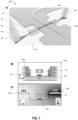
Figure 1 is a diagrammatic representation of an embodiment of an integrated optomechanical microwave clock according to the invention. Theoptomechanical clock 100 comprises anoptical waveguide 102 arranged on achip 103, or semiconductor platform. Theoptomechanical clock 100 also comprises a nano-cavity 101 arranged substantially parallel to theoptical waveguide 102. - In the embodiment as illustrated in
Figure 1 , the nano-cavity 101 comprises a GaP optomechanical crystal. The nano-cavity 101 is referred to as a nanobeam. It is fabricated on top of a Silicon-on-Insulator (SoI) photonics circuit. Theoptomechanical clock 100 also comprises a pair ofelectrodes electrode nanobeam 101, at a distance to thenanobeam 101. - This SoI platform comprises at least one silicon (Si)
waveguide 102. In particular, the platform may comprise several pre-defined silicon waveguides. The at least onewaveguide 102 hasoptical gratings 105 at each end, allowing for the coupling of optical signal from and tooptical fibers 106. -
Figure 1a ) shows a schematic view of theoptomechanical clock 100 withoptical fibers 106 positioned above thewaveguide gratings 105. -
Figure 1b ) is a cross-sectional view of theoptomechanical clock 100 showing its different layers as well as the position of theelectrodes nanobeam 101. - The
nanobeam 101 is preferably made of a III-V semiconductor material, such as GaP, GaAs, InP, or InxGa1-xP. - Through their parallel arrangement, reproducible and efficient evanescent coupling between the
Si waveguide 102 and the III-V cavity 101 may be achieved. - The
nanobeam 101 is suspended in the air, parallel with respect to theSi waveguide 102, by means of twoanchors 107 located at the respective ends of thenanobeam 101. With reference toFigure 1b ), a SiN layer 109 below the GaP layer keeps the GaP layer (of which thenanobeam 101 is made) raised so as not to touch theSi waveguide 102. Once the GaP layer has been dry-etched, the SiN layer is removed under thenanobeam 101. Thenanobeam 101 is thus suspended while theanchors 107 remain set on the SiN layer. - The electric field between the
electrodes nanobeam 101. The simulated electric field is illustrated in Figure 1d) with arrows, and the electric potential with a grey scale. - Preferably, the nano-
cavity 101 is a photonic crystal (PhC) cavity. It is specifically designed for optical and mechanical modes to overlap, resulting in high optomechanical coupling rates. Geometric design parameters are the height of elliptical holes and the adjacent-hole distance of the crystal. In an example, both are increasing by following a Gaussian distribution with each step from the cavity centre to the mirror section at the ends of thenanobeam 101. These end sections are composed of identical and equally spaced holes that act as a mirror for the targeted optical and mechanical frequencies. This co-design results in a good confinement of both the optical modes and the GHz mechanical modes in the nano-cavity 101. - The mechanical motion of the
nanobeam 101 modulates the light coupled to the nano-cavity 101 and this modulation gets imprinted on the light exiting the nano-cavity 101 into thewaveguide 102. The output optical signal may then be read with a photodiode and an electrical spectrum analyzer. - A typical electrical spectrum in the 0-4 GHz range is shown on
Figure 2 . The peaks up to 500 MHz on the recorded spectrum correspond to mechanical modes not confined in the nano-cavity, with displacement fields along the full length of the photonic wire, or nanobeam. The peak at 3.35 GHz, on the other hand, corresponds to a localized mechanical mode. - The nanobeam may be mechanical excited using different excitation means.
- According to a first example, a mechanical mode in the nano-cavity may be excited by injecting a single-mode laser in the nanobeam through the Si waveguide around the resonance wavelength. This leads to the excitation of the mechanical eigenmodes of the PhC.
- An important figure of merit of the spectral purity of the mechanical mode is the phase noise, which gives information on the linewidth and the short-term stability of the oscillation. The phase noise depends on the wavelength detuning from the resonance and the optical powers injected.
- According to a second example, a mechanical mode in the nano-cavity may be excited by actuating the on-chip electrodes. This electro-mechanical actuation of the nanobeam can be achieved because of the piezoelectric properties of GaP. Thus, in order to optimize electro-mechanical coupling without disturbing the optical field, the nanobeam is placed between the two electrodes, aligned with respect to the centre of the nano-cavity. The electrodes may be, for example, 1 µm wide gold electrodes. The electrode-to-nanobeam side distance may be 1 µm. When a potential is applied at the electrodes, they create a transverse electric field across the nanobeam. Actuation efficiency can be optimized with a field oriented along the longitudinal direction of the nanobeam; however, this configuration would need a complicated fabrication process.
- Applying a periodic signal on the electrodes while coupling laser light close to the resonance of the nanobeam allows observing the electro-mechanical actuation transduced into the optical domain. When the driving frequency is close to the self-sustained oscillation of the nanobeam, the self-sustained oscillation locks on the signal generator, wherein a higher injected electrical power induces a wider locking range.
- The optomechanical clock according to the present invention further comprises mode-lock means. These mode-lock means allow for locking either or both of the optical and mechanical modes of the nano-cavity. Embodiments of mode-lock means are described in the following with reference to
Figures 3 to 5 . -
Figure 3 is a diagrammatic representation of an embodiment of anoptomechanical clock 200 according to the present invention. In this embodiment, the mode-lock means comprise a radio-frequency resonant LC circuit. This RF LC circuit constitutes an electrical excitation means, generating a frequency corresponding to the frequency of the mechanical mode of the nano-cavity 201. - The RF LC circuit comprises an
integrated inductance 208 andcapacitor 209 allowing for an electronic resonance at the same frequency as the mechanical mode frequency. The circuit is coupled to thenanobeam 101 by a pair ofelectrodes Figure 1a ). Theinductance 208 may be formed by a spiral of metal wire, for example the same metal as the one used for theelectrodes capacitor 209 may be implemented by metallic interdigitated electrodes. - As mentioned above, the piezoelectric coefficient of the material used for the
nanobeam 101 allows a mechanical displacement induced by an electrical excitation. To efficiently excite and enhance the mechanical displacement at the mechanical frequency of the mode (e.g., 3.4 GHz), an electrical resonance at the exact same frequency is mandatory. The dimensions and the metal used for the RF LC circuit allow to adjust the RF frequency close to the one of thenanobeam 101. This resonant effect improves the efficiency of the mode-lock means. -
Figure 4 is a diagrammatic representation of another embodiment of anoptomechanical clock 300 according to the present invention. In this embodiment, the mode-lock means comprise radio-frequency acoustic excitation means, and in particular an RFacoustic generator 310. The RFacoustic generator 310 realizes an electromechanical excitation in a distance from thenanobeam 101. The acoustic generator may be implemented by an on-chip interdigitated electrode with a sub-micron spacing which controls the RF frequency. The spacing has to be adjusted in order to have a frequency matching with the frequency of the mechanical mode of the nanobeam101. - The
RF generator 310 is coupled to anacoustic waveguide 311, preferably an on-chip acoustic waveguide. As represented inFigure 4 , the mode-lock means comprise also an acousticpassive loop 312 to which theacoustic waveguide 311 is coupled. The acousticpassive loop 312 may comprise an additional acoustic waveguide, which also is preferably an on-chip acoustic waveguide. - Thanks to the piezoelectric electric coefficient of the material, the interdigitated
electrode 310 generates an acoustic wave at the frequency of thenanobeam 101. The frequency is adjusted with the geometrical parameters of theRF generator 310 and the material used. Theacoustic waveguide 311 is used to collect the acoustical energy going out of the interdigitatedelectrode 310 and to route it towards the acousticpassive loop 312. The acoustic confinement is done by engineering the acoustic dispersion in and perpendicularly to the propagating direction of the acoustical wave. The control of the coupling between theacoustic waveguide 311 and the acousticpassive loop 312 can be realized by the relative distance between them. The frequency of the optomechanical clock is injection-locked by the acoustic wave with a delay induced by thepassive loop 312. -
Figure 5 is a diagrammatic representation of another embodiment of anoptomechanical clock 400 according to the present invention. In this embodiment, the mode-lock means comprise an optical frequency-comb generator 420. Thisgenerator 420 is an optical micrometer-size resonator made of a material with nonlinear properties. To overcome the material dispersion, group-velocity dispersion has to be engineered by adjusting the geometrical parameters of the micrometer-size resonator. - The optical frequency-
comb generator 420 is optically coupled to the sameoptical waveguide 102 as thenanobeam 101. The injected laser light generates an optical frequency comb of which one of the lines addresses the resonance ofnanobeam 101. By adjusting the power and the wavelength of the injected laser light, the spacing and stability of the frequency comb can be adjusted. The resonance of thenanobeam 101 will be locked to the stabilized light line, improving the overall phase-noise performances of theoptomechanical clock 400. - The mode-lock means according to the embodiments detailed with respect to
Figures 3 to 5 may be combined with each other in an optomechanical clock. - Of course, the invention is not limited to the examples detailed above.
Claims (13)
- An optomechanical microwave clock (100, 200, 300, 400) integrated on a chip (103), comprising:- an optical waveguide (102) arranged on the chip (103),- a nano-cavity (101) arranged substantially parallel to the optical waveguide (102),wherein an optical mode excited in the nano-cavity (101) is modulated at an oscillation frequency of a mechanical mode of the nano-cavity (101), the modulated optical mode being evanescently coupled to the optical waveguide (102) in at least one coupling region;wherein the optomechanical clock (100, 200, 300, 400) further comprises:- mode-lock means configured to control the optomechanical oscillation stability of the optomechanical microwave clock.
- The optomechanical clock (100, 200, 300, 400) according to claim 1, characterized in that it further comprises a pair of electrodes (104a, 104b) configured to produce an electrical field through the nano-cavity (101), wherein one electrode (104a, 104b) is arranged on-chip on either of the longitudinal sides of the nano-cavity (101).
- The optomechanical clock (100, 200, 300, 400) according to claim 1 or 2, characterized in that the mode-lock means comprise a radio-frequency electric excitation means oscillating at the frequency of the mechanical mode of the nano-cavity.
- The optomechanical clock (200) according to any one of the preceding claims, characterized in that the radio-frequency electric excitation means comprise a radio-frequency LC circuit (208, 209).
- The optomechanical clock (300) according to any one of the preceding claims, characterized in that the mode-lock-means comprises radio-frequency acoustic excitation means (310, 311, 312) oscillating at the frequency of the mechanical mode of the nano-cavity (101).
- The optomechanical clock (300) according to the preceding claim, characterized in that the radio-frequency acoustic excitation means comprises an acoustic passive loop (312).
- The optomechanical clock (300) according to the preceding claim, characterized in that the acoustic passive loop (312) comprises an acoustic waveguide.
- The optomechanical clock (400) according to any one of the preceding claims, characterized in that the mode-lock-means comprises an optical frequency-comb generator (420).
- The optomechanical clock (100, 200, 300, 400) according to any of the preceding claims, characterized in that the optical waveguide (102) is a silicon waveguide.
- The optomechanical clock (100, 200, 300, 400) according to any of the preceding claims, wherein the nano-cavity (101) is suspended in the air parallel above the optical waveguide (102) by means of anchoring means (107).
- The optomechanical clock (100, 200, 300, 400) according to any of the preceding claims, wherein the nano-cavity (101) comprises a photonic crystal.
- The optomechanical clock (100, 200, 300, 400) according to the preceding claim, characterized in that the photonic crystal is a GaP photonic crystal.
- The optomechanical clock (100, 200, 300, 400) according to any of the preceding claims, characterized in that the chip (103) comprises a silicon-on-insulator substrate.
Priority Applications (3)
| Application Number | Priority Date | Filing Date | Title |
|---|---|---|---|
| EP23306726.3A EP4535656A1 (en) | 2023-10-06 | 2023-10-06 | Optomechanical integrated microwave clock |
| CN202480063474.2A CN121970249A (en) | 2023-10-06 | 2024-10-04 | Opto-mechanical integrated microwave clock |
| PCT/EP2024/078040 WO2025073955A1 (en) | 2023-10-06 | 2024-10-04 | Optomechanical integrated microwave clock |
Applications Claiming Priority (1)
| Application Number | Priority Date | Filing Date | Title |
|---|---|---|---|
| EP23306726.3A EP4535656A1 (en) | 2023-10-06 | 2023-10-06 | Optomechanical integrated microwave clock |
Publications (1)
| Publication Number | Publication Date |
|---|---|
| EP4535656A1 true EP4535656A1 (en) | 2025-04-09 |
Family
ID=88839543
Family Applications (1)
| Application Number | Title | Priority Date | Filing Date |
|---|---|---|---|
| EP23306726.3A Pending EP4535656A1 (en) | 2023-10-06 | 2023-10-06 | Optomechanical integrated microwave clock |
Country Status (3)
| Country | Link |
|---|---|
| EP (1) | EP4535656A1 (en) |
| CN (1) | CN121970249A (en) |
| WO (1) | WO2025073955A1 (en) |
Citations (4)
| Publication number | Priority date | Publication date | Assignee | Title |
|---|---|---|---|---|
| CN107863676A (en) * | 2017-11-22 | 2018-03-30 | 中国科学院西安光学精密机械研究所 | Optical soliton crystal optical frequency comb generation system and method based on microring resonator |
| US20210058033A1 (en) * | 2017-10-17 | 2021-02-25 | Thales | Radio frequency oscillator |
| CN112751251A (en) * | 2020-12-29 | 2021-05-04 | 南京南辉智能光学感控研究院有限公司 | Double-optical frequency comb generation system and generation method |
| CN113916807A (en) * | 2021-08-27 | 2022-01-11 | 浙江工业大学 | Micro-cavity optical frequency comb gas concentration sensing measurement method |
-
2023
- 2023-10-06 EP EP23306726.3A patent/EP4535656A1/en active Pending
-
2024
- 2024-10-04 WO PCT/EP2024/078040 patent/WO2025073955A1/en active Pending
- 2024-10-04 CN CN202480063474.2A patent/CN121970249A/en active Pending
Patent Citations (4)
| Publication number | Priority date | Publication date | Assignee | Title |
|---|---|---|---|---|
| US20210058033A1 (en) * | 2017-10-17 | 2021-02-25 | Thales | Radio frequency oscillator |
| CN107863676A (en) * | 2017-11-22 | 2018-03-30 | 中国科学院西安光学精密机械研究所 | Optical soliton crystal optical frequency comb generation system and method based on microring resonator |
| CN112751251A (en) * | 2020-12-29 | 2021-05-04 | 南京南辉智能光学感控研究院有限公司 | Double-optical frequency comb generation system and generation method |
| CN113916807A (en) * | 2021-08-27 | 2022-01-11 | 浙江工业大学 | Micro-cavity optical frequency comb gas concentration sensing measurement method |
Non-Patent Citations (6)
| Title |
|---|
| HAN ZHAO ET AL: "Electro-optic transduction in silicon via GHz-frequency nanomechanics", ARXIV.ORG, CORNELL UNIVERSITY LIBRARY, 201 OLIN LIBRARY CORNELL UNIVERSITY ITHACA, NY 14853, 24 October 2022 (2022-10-24), XP091352533 * |
| LAUDE VINCENT: "Phoxonic crystals for harnessing the interaction of light and sound", 2016 INTERNATIONAL CONFERENCE ON OPTICAL MEMS AND NANOPHOTONICS (OMN), IEEE, 31 July 2016 (2016-07-31), pages 1 - 2, XP032960115, DOI: 10.1109/OMN.2016.7565814 * |
| LAURA MERCAD\'E ET AL: "Photonic Frequency Conversion of OFDM Microwave Signals in a Wavelength-Scale Optomechanical Cavity", ARXIV.ORG, CORNELL UNIVERSITY LIBRARY, 201 OLIN LIBRARY CORNELL UNIVERSITY ITHACA, NY 14853, 16 December 2021 (2021-12-16), XP091120752, DOI: 10.1002/LPOR.202100175 * |
| MIDOLO LEONARDO ET AL: "Nano-opto-electro-mechanical systems", ARXIV.ORG, NATURE PUB. GROUP, INC, LONDON, vol. 13, no. 1, 9 January 2018 (2018-01-09), pages 11 - 18, XP036429618, ISSN: 1748-3387, [retrieved on 20180109], DOI: 10.1038/S41565-017-0039-1 * |
| NAVARRO-URRIOS D ET AL: "Room-temperature silicon platform for GHz-frequency nano-electro-opto-mechanical systems", ARXIV.ORG, CORNELL UNIVERSITY LIBRARY, 201 OLIN LIBRARY CORNELL UNIVERSITY ITHACA, NY 14853, 18 October 2021 (2021-10-18), XP091077201 * |
| ROBERT STOCKILL ET AL: "Ultra-low-noise Microwave to Optics Conversion in Gallium Phosphide", ARXIV.ORG, CORNELL UNIVERSITY LIBRARY, 201 OLIN LIBRARY CORNELL UNIVERSITY ITHACA, NY 14853, 25 November 2022 (2022-11-25), XP091377202, DOI: 10.1038/S41467-022-34338-X * |
Also Published As
| Publication number | Publication date |
|---|---|
| CN121970249A (en) | 2026-05-01 |
| WO2025073955A1 (en) | 2025-04-10 |
Similar Documents
| Publication | Publication Date | Title |
|---|---|---|
| US8031012B2 (en) | Optoelectronic oscillator and pulse generator | |
| US7062131B2 (en) | Optical coupling for whispering-gallery-mode resonators via waveguide gratings | |
| JP4163630B2 (en) | Atomic clock based on opto-electronic oscillator | |
| Sohler et al. | Integrated optical devices in lithium niobate | |
| CN101911403B (en) | Cross modulation-based opto-electronic oscillator with tunable electro-optic optical whispering gallery mode resonator | |
| US6567436B1 (en) | Opto-electronic oscillators having optical resonators | |
| US6928091B1 (en) | Opto-electronic oscillator including a tunable electro-optic filter | |
| US7050212B2 (en) | Active mode-locked lasers and other photonic devices using electro-optic whispering gallery mode resonators | |
| US7215848B2 (en) | Optical isolator utilizing a micro-resonator | |
| WO2014197780A1 (en) | Low-noise microwave-frequency generator | |
| JP2006511841A (en) | Tunable optical filter | |
| US9122004B1 (en) | Heterogeneous resonant photonic integrated circuit | |
| EP2312388A2 (en) | All-optical memory latch using nonlinear elements | |
| US11171606B2 (en) | Radio frequency oscillator | |
| US9036951B2 (en) | Silicon acousto-optic modulator structure and method | |
| CN115453690B (en) | A high-Q microdisk resonator with active mode selection | |
| WO2025073955A1 (en) | Optomechanical integrated microwave clock | |
| Do et al. | Silicon photonic spiral shape resonator applied to the optoelectronic oscillator | |
| Maleki | Recent progress in opto-electronic oscillator | |
| JPS63231403A (en) | Optical apparatus having light waveguide | |
| Zhang et al. | Surface acoustic wave lasing in a silicon optomechanical cavity | |
| Bortsov et al. | Nanostructural optoelectronic oscillators with the fiber-optical delay line | |
| Perego et al. | 7 Optical frequency combs in | |
| CN121879014A (en) | Thin film lithium niobate electro-optical modulator and method based on electromagnetic induction-like transparent effect | |
| Yan et al. | Wideband-tunable integrated microwave photonic filter based on an ultra-high-Q resonator |
Legal Events
| Date | Code | Title | Description |
|---|---|---|---|
| PUAI | Public reference made under article 153(3) epc to a published international application that has entered the european phase |
Free format text: ORIGINAL CODE: 0009012 |
|
| STAA | Information on the status of an ep patent application or granted ep patent |
Free format text: STATUS: THE APPLICATION HAS BEEN PUBLISHED |
|
| AK | Designated contracting states |
Kind code of ref document: A1 Designated state(s): AL AT BE BG CH CY CZ DE DK EE ES FI FR GB GR HR HU IE IS IT LI LT LU LV MC ME MK MT NL NO PL PT RO RS SE SI SK SM TR |
|
| STAA | Information on the status of an ep patent application or granted ep patent |
Free format text: STATUS: REQUEST FOR EXAMINATION WAS MADE |
|
| 17P | Request for examination filed |
Effective date: 20251009 |