EP4535561A1 - Antenna structure - Google Patents
Antenna structure Download PDFInfo
- Publication number
- EP4535561A1 EP4535561A1 EP23814675.7A EP23814675A EP4535561A1 EP 4535561 A1 EP4535561 A1 EP 4535561A1 EP 23814675 A EP23814675 A EP 23814675A EP 4535561 A1 EP4535561 A1 EP 4535561A1
- Authority
- EP
- European Patent Office
- Prior art keywords
- segment
- gap
- antenna structure
- radiation sheet
- feeder
- Prior art date
- Legal status (The legal status is an assumption and is not a legal conclusion. Google has not performed a legal analysis and makes no representation as to the accuracy of the status listed.)
- Pending
Links
Images


Classifications
-
- H—ELECTRICITY
- H01—ELECTRIC ELEMENTS
- H01Q—ANTENNAS, i.e. RADIO AERIALS
- H01Q1/00—Details of, or arrangements associated with, antennas
- H01Q1/36—Structural form of radiating elements, e.g. cone, spiral, umbrella; Particular materials used therewith
- H01Q1/38—Structural form of radiating elements, e.g. cone, spiral, umbrella; Particular materials used therewith formed by a conductive layer on an insulating support
-
- H—ELECTRICITY
- H01—ELECTRIC ELEMENTS
- H01Q—ANTENNAS, i.e. RADIO AERIALS
- H01Q19/00—Combinations of primary active antenna elements and units with secondary devices, e.g. with quasi-optical devices, for giving the antenna a desired directional characteristic
- H01Q19/10—Combinations of primary active antenna elements and units with secondary devices, e.g. with quasi-optical devices, for giving the antenna a desired directional characteristic using reflecting surfaces
- H01Q19/104—Combinations of primary active antenna elements and units with secondary devices, e.g. with quasi-optical devices, for giving the antenna a desired directional characteristic using reflecting surfaces using a substantially flat reflector for deflecting the radiated beam, e.g. periscopic antennas
-
- H—ELECTRICITY
- H01—ELECTRIC ELEMENTS
- H01Q—ANTENNAS, i.e. RADIO AERIALS
- H01Q9/00—Electrically-short antennas having dimensions not more than twice the operating wavelength and consisting of conductive active radiating elements
- H01Q9/04—Resonant antennas
- H01Q9/06—Details
- H01Q9/065—Microstrip dipole antennas
-
- H—ELECTRICITY
- H01—ELECTRIC ELEMENTS
- H01Q—ANTENNAS, i.e. RADIO AERIALS
- H01Q1/00—Details of, or arrangements associated with, antennas
- H01Q1/50—Structural association of antennas with earthing switches, lead-in devices or lightning protectors
-
- H—ELECTRICITY
- H01—ELECTRIC ELEMENTS
- H01Q—ANTENNAS, i.e. RADIO AERIALS
- H01Q13/00—Waveguide horns or mouths; Slot antennas; Leaky-waveguide antennas; Equivalent structures causing radiation along the transmission path of a guided wave
- H01Q13/10—Resonant slot antennas
-
- H—ELECTRICITY
- H01—ELECTRIC ELEMENTS
- H01Q—ANTENNAS, i.e. RADIO AERIALS
- H01Q21/00—Antenna arrays or systems
- H01Q21/0006—Particular feeding systems
-
- H—ELECTRICITY
- H01—ELECTRIC ELEMENTS
- H01Q—ANTENNAS, i.e. RADIO AERIALS
- H01Q21/00—Antenna arrays or systems
- H01Q21/30—Combinations of separate antenna units operating in different wavebands and connected to a common feeder system
-
- H—ELECTRICITY
- H01—ELECTRIC ELEMENTS
- H01Q—ANTENNAS, i.e. RADIO AERIALS
- H01Q9/00—Electrically-short antennas having dimensions not more than twice the operating wavelength and consisting of conductive active radiating elements
- H01Q9/04—Resonant antennas
- H01Q9/16—Resonant antennas with feed intermediate between the extremities of the antenna, e.g. centre-fed dipole
-
- H—ELECTRICITY
- H01—ELECTRIC ELEMENTS
- H01Q—ANTENNAS, i.e. RADIO AERIALS
- H01Q9/00—Electrically-short antennas having dimensions not more than twice the operating wavelength and consisting of conductive active radiating elements
- H01Q9/04—Resonant antennas
- H01Q9/16—Resonant antennas with feed intermediate between the extremities of the antenna, e.g. centre-fed dipole
- H01Q9/28—Conical, cylindrical, cage, strip, gauze, or like elements having an extended radiating surface; Elements comprising two conical surfaces having collinear axes and adjacent apices and fed by two-conductor transmission lines
- H01Q9/285—Planar dipole
Definitions
- the embodiment of the present disclosure provides an antenna structure, comprising:
- a length of a side of the second part away from the gap is less than a distance between the first end of the second part and the second end of the second part.
- a length of a side of the fourth part away from the gap is less than a distance between the first end of the fourth part and the second end of the fourth part.
- the first segment is parallel to the gap, a projection of the first segment on the first surface is located on the first radiation sheet, and the second segment is perpendicular to the gap and the projection on the first surface spans the gap.
- the feeder comprises a first segment, a second segment and a third segment; one end of the first segment corresponds to the first end of the feeder, one end of the second segment is connected with the other end of the first segment, the other end of the second segment is connected with one end of the third segment, the other end of the third segment is coupled with the first radiation sheet and the second radiation sheet, and the excitation signal is fed into the first radiation sheet and the second radiation sheet in the mode of coupling feeding.
- the first segment and the third segment are parallel to the gap, and a projection of the first segment on the first surface is located at the first radiation sheet, a projection of the third segment on the first surface is located at the second radiation sheet, and a projection of the second segment on the first surface spans the gap.
- the feeder comprises a microstrip feeder.
- the purpose of the present disclosure is to provide an antenna structure in which the width of the main lobe of the pattern in the whole frequency band can be basically the same, that is, the broadband characteristics of the pattern, through the coexistence of two radiation modes of the slot antenna and the dipole antenna.
- an antenna structure includes a dielectric substrate 10, a first radiation sheet 11, a second radiation sheet 12 and a feeder 14.
- the dielectric substrate 10 includes a first surface and a second surface on opposite sides.
- the first radiation sheet 11 is arranged on the first surface
- the second radiation sheet 12 is arranged on the first surface.
- the first radiation sheet 11 and the second radiation sheet 12 are metal sheets.
- the first radiometer 11 comprises a first part A and a second part B connected to the first part A
- the second radiometer 12 comprises a third part C and a fourth part D connected to the third part C.There is a gap 13 between the first radiation sheet 11 and the second radiation sheet 12.
- the antenna structure according to an embodiment of the present disclosure proposes the slot antenna and the dipole antenna with the two radiation modes, so that the antenna structure operates with two different radiation principles, i.e., the high frequency corresponds to the slot antenna radiation, and the low frequency corresponds to the dipole antenna radiation.
- the width of the main lobe of the pattern in the whole frequency band is basically the same, realizing the broadband characteristics of the pattern.
- the antenna structure further includes a reflector 20 perpendicular to the dielectric substrate 10.
- the reflector 20 is equally divided into a first reflection area 21 and a second reflection area 22.
- the first reflection area 21 is close to the first surface
- the second reflection area 22 is close to the second surface.
- a feed port 23 is arranged on the second reflection area 22, and the first end of the feeder 14 is connected with the feed port 23.
- the dielectric substrate 10 which is an FR4 dielectric plate with a thickness of 1.6mm has advantages of low cost, high process precision, and good consistency.
- the gap 13 has a horn-shaped notch in a direction away from the first part A and the third part C.
- the second part B and the fourth part D close to the gap 13 are symmetrically oblique to form a horn-shaped notch at one end of the gap 13.
- the first part A comprises a first end and a second end
- the second part B comprises a first end and a second end.
- the second end of the second part B is connected to the first end of the first part A.
- a width d of the second end of the second part B is greater than a width b of the first end of the first part A, as shown in Fig. 3 .
- the width of the first part A gradually increases along the gap 13 in the direction away from the second part B.
- the second part B and the fourth part D form the dipole antenna.
- the second part B and the fourth part D are equivalent to two antenna arms, and a length d of the antenna arm in the present embodiment can be 22mm.
- the length of the side of the second part B away from the gap 13 is shorter than the distance between the first end of the second part B and the second end of the second part B, i.e., f labeled in Fig. 3 is less than g.
- the second part B and the fourth part D are symmetrically arranged with the gap 13 as the axis of symmetry, the side of the fourth part D away from the gap 13 is shorter than the distance between the first end of the fourth part D and the second end of the fourth part D. Differing from an antenna arm of conventional dipole antenna, the second part B and the fourth part D in the side away from the gap 13 is obliquely cut, i.e. the outer side of the second part B and the fourth part D is chamfered, so that the resonant current is directed towards the reflector 20 at a certain inclination angle.
- the feeder 14 comprises the first segment 141 and the second segment 142.
- the dielectric substrate 10 is provided with vias 30.
- the first segment 141 is arranged along the direction parallel to the second surface and the gap 13.
- One end of the first segment 141 is arranged on the edge of the dielectric substrate 10 and is connected with the feed port 23 on the reflector 20.
- a projection of one end of the first segment 141 on the first surface is located in the first part A, and a projection of the other end of the first segment 141 on the first surface is located in the second part B.
- One end of the first segment 141 corresponds to the first end of the feeder 14, the other end of the first segment 141 is connected with one end of the second segment 142.
- the other end of the second segment 142 is connected with the first radiation sheet 11 through via 30.
- the first segment 141 is parallel to the gap 13.
- a projection of the first segment 141 on the first surface is located on the first radiation sheet 11.
- the second segment 142 is perpendicular to the gap 13 and the projection on the first surface spans the gap 13.
- the feeder 14 in this embodiment is locally short-circuited with the first radiation sheet 11 on the first surface of the dielectric substrate 10 through a via 30 to form a strong feeder structure.
- the feeder comprises the first, second, and third segments.
- the first segment is arranged along the direction parallel to the gap 13 along the second surface.
- One end of the first segment is arranged on the edge of the dielectric substrate 10 and is connected with the feed port 23 on the reflector 20.
- the projection of one end of the first segment on the first surface is located in the first part A, and the projection of the other end of the first segment on the first surface is located in the second part B.
- One end of the first segment corresponds to the first end of the feeder.
- One end of the second segment is connected with the other end of the first segment, and the other end of the second segment is connected with one end of the third segment.
- the other end of the third segment is coupled with the first radiation sheet 11 and the second radiation sheet 12.
- the excitation signal is fed to the first radiation sheet 11 and the second radiation sheet 12 in the mode of coupling feeding.
- the first segment and the third segment are parallel to the gap 13.
- the projection of the first segment on the first surface is located at the first radiation sheet 11.
- the projection of the third segment on the first surface is located at the second radiation sheet 12.
- the projection of the second segment on the first surface spans the gap 13. That is, in this embodiment, because no via 30 is set on the dielectric substrate 10, the second segment of the feeder is extended to form the third segment.
- One end of the third segment is connected with the other end of the second segment, and the other end of the third segment extends a suitable length along the second surface to the position where the reflector 20 is located, so as to form of a coupled feeding structure.
- Fig. 5 illustrates a VSWR curve of the antenna structure in Fig. 2 .
- the Voltage Standing Wave Ratio (VSWR) of the antenna structure is less than or equal to the impedance bandwidth of 4.3GHz-8.47GHz in the full frequency band, the relative bandwidth is 65%, and the half-power width of the pattern in the frequency band is similar.
- VSWR Voltage Standing Wave Ratio
- Fig. 6 , Fig. 7 and Fig. 8 illustrate 2D patterns of radiation operating at 5.01 GHz, 6.5 GHz and 7.12 GHz, respectively, according to the antenna structure illustrated in Fig. 2 .
- the inner curve represents the E plane and the outer curve represents the H plane.
- the H-plane and the E-plane are two reference planes that are orthogonal to each other, and the 3DB beamwidth of the E-plane is less than 3dB in the whole frequency band from 73° ⁇ 86°, and the normal ⁇ 35° range.
- the 3dB beam width on the H-plane is about 180°.
- the antenna structure according to the present disclosure includes a slot antenna and a dipole antenna.
- the antenna structure can transition from the working mode of the dipole antenna to the slot working mode from low frequency to high frequency, which can not only realize the ultra-wide frequency band, but also help to maintain the basic consistency of the pattern in the ultra-wide range.
- an antenna structure includes a dielectric substrate comprising a first surface and a second surface opposite, a first radiation sheet arranged on the first surface and comprising a first part and a second part connected with the first part, a second radiation sheet arranged on the first surface and comprising a third part and a fourth part connected with the third part, and a feeder.
- a gap is between the second radiation sheet and the first radiation sheet.
- the feeder is arranged on the second surface and comprises a first end for inputting an excitation signal and a second end for feeding an excitation signal to the first radiation sheet and the second radiation sheet.
- the first part, the third part and the gap form a slot antenna
- the second part and the fourth part form a dipole antenna.
- the antenna structure can transition from the working mode of the dipole antenna to the working mode of the slot mode from the low frequency to high frequency, which can not only realize the ultra-wide frequency band, but also maintain the basic consistency of the pattern beamwidth in the wide range.
Landscapes
- Waveguide Aerials (AREA)
Abstract
Description
- This application claims priority to
Chinese Application No. 202210611123.3, entitled "Antenna structure", filed on May 31, 2022 - The present disclosure relates to the field of antenna technology, in particular to an antenna structure.
- At present, the beacon antenna mostly adopts the horn antenna. Because the high and low frequencies of the horn antenna are the same radiation port surface, the corresponding radiation pattern of the beamwidth is acute in the high frequency range and narrow beam significantly caused by the common port surface.
- The beamwidth changes greatly as a change of frequency, resulting in a large change in the antenna gain, which makes the pattern of the directional radiation region of the antenna have poor broadband characteristics.
- The purpose of the present disclosure is to provide an antenna structure in which the width of the main lobe of the pattern in the whole frequency band, i.e. the broadband characteristics of the pattern, can be basically the same through the coexistence of two radiation modes of the slot antenna and the dipole antenna.
- In order to achieve the above purpose, the present disclosure provides the following technical scheme:
- The embodiment of the present disclosure provides an antenna structure, comprising:
- a dielectric substrate, comprising a first surface and a second surface opposite;
- a first radiation sheet, arranged on the first surface, comprising a first part and a second part connected with the first part;
- a second radiation sheet, arranged on the first surface, comprising a third part and a fourth part connected with the third part, where a gap is between the second radiation sheet and the first radiation sheet;
- a feeder, arranged on the second surface, comprising a first end for inputting an excitation signal and a second end for feeding an excitation signal to the first radiation sheet and the second radiation sheet;
- wherein the first part, the third part and the gap form a slot antenna, and the second part and the fourth part form a dipole antenna.
- In some embodiments, the first part and the third part are symmetrical with the gap as an axis of symmetry to form a broadband balun structure.
- In some embodiments, the gap expands in a direction away from the first part and the third part to form a horn-shaped notch.
- In some embodiments, the first part comprises a first end and a second end, the second part comprises a first end and a second end, and the second end of the second part is connected with the first end of the first part.
- In some embodiments, a width of the second end of the second part is greater than a width of the first end of the first part.
- In some embodiments, a width of the first part gradually increases along the gap in the direction away from the second part.
- In some embodiments, a width of the third part gradually increases along the gap in the direction away from the fourth part.
- In some embodiments, a curved line is along an edge of one side of the first part away from the gap.
- In some embodiments, the edge of one side away from the gap in the third part is an arc-shaped line.
- In some embodiments, a length of a side of the second part away from the gap is less than a distance between the first end of the second part and the second end of the second part.
- In some embodiments, a length of a side of the fourth part away from the gap is less than a distance between the first end of the fourth part and the second end of the fourth part.
- In some embodiments, the feeder comprises a first segment and a second segment, and a via is arranged on the dielectric substrate; one end of the first segment corresponds to the first end of the feeder, the other end of the first segment is connected with one end of the second segment, and the other end of the second segment is connected with the first radiation sheet through the via.
- In some embodiments, the first segment is parallel to the gap, a projection of the first segment on the first surface is located on the first radiation sheet, and the second segment is perpendicular to the gap and the projection on the first surface spans the gap.
- In some embodiments, the feeder is partially short-circuited with the first radiation sheet of the first surface through the via.
- In some embodiments, the feeder comprises a first segment, a second segment and a third segment; one end of the first segment corresponds to the first end of the feeder, one end of the second segment is connected with the other end of the first segment, the other end of the second segment is connected with one end of the third segment, the other end of the third segment is coupled with the first radiation sheet and the second radiation sheet, and the excitation signal is fed into the first radiation sheet and the second radiation sheet in the mode of coupling feeding.
- In some embodiments, the first segment and the third segment are parallel to the gap, and a projection of the first segment on the first surface is located at the first radiation sheet, a projection of the third segment on the first surface is located at the second radiation sheet, and a projection of the second segment on the first surface spans the gap.
- In some embodiments, the feeder comprises a microstrip feeder.
- In some embodiments, the antenna structure further includes a reflector which is equally divided to form a first reflection area and a second reflection area. The dielectric substrate is perpendicular to the reflector, the first reflection area is close to the first surface, and the second reflection area is close to the second surface.
- In some embodiments, a feeder port is arranged on the second reflective area, and the first end of the feeder is connected with the feeder port.
- In some embodiments, the dielectric substrate is an FR4 dielectric plate.
- In contrast to prior art, the present disclosure provides an antenna structure that includes a slot antenna and a dipole antenna. The antenna structure can switch from the working mode of the dipole antenna to the working mode of the slot antenna from low frequency to high frequency from, which can not only realize the wide frequency band, but also maintain the basic consistency of the pattern in the wide frequency band, so as to realize the broadband characteristics of the pattern and ensure that the antenna beam width is basically consistent.
-
-
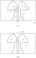
Fig. 1 is a schematic diagram of the antenna structure according to an embodiment of the present disclosure. -
Fig. 2 is a schematic diagram of the three-dimensional structure of the antenna structure according to an embodiment of the present disclosure. -
Fig. 3 is a schematic diagram of the antenna structure according to an embodiment of the present disclosure. -
Fig. 4 is a schematic diagram of the feeder of the antenna structure according to an embodiment of the present disclosure. -
Fig. 5 illustrates the VSWR curve of the antenna structure according to an embodiment of the present disclosure. -
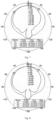
Fig. 6 ,Fig. 7 and Fig. 8 depict the antenna structure at different frequency points for the present disclosure. - The purpose of the present disclosure is to provide an antenna structure in which the width of the main lobe of the pattern in the whole frequency band can be basically the same, that is, the broadband characteristics of the pattern, through the coexistence of two radiation modes of the slot antenna and the dipole antenna.
- In order to make the purpose, technical scheme and effect of the present disclosure clearer and more definite, the present disclosure is further described in detail below with reference to the accompanying drawings and embodiments. It should be understood that the specific embodiments described herein are used only to interpret the present disclosure and are not intended to qualify the present disclosure.
- Referring to
FIG. 1 , an antenna structure includes adielectric substrate 10, afirst radiation sheet 11, asecond radiation sheet 12 and afeeder 14. Thedielectric substrate 10 includes a first surface and a second surface on opposite sides. Thefirst radiation sheet 11 is arranged on the first surface, and thesecond radiation sheet 12 is arranged on the first surface. Thefirst radiation sheet 11 and thesecond radiation sheet 12 are metal sheets. Thefirst radiometer 11 comprises a first part A and a second part B connected to the first part A, and thesecond radiometer 12 comprises a third part C and a fourth part D connected to the third part C.There is agap 13 between thefirst radiation sheet 11 and thesecond radiation sheet 12. Thefeeder 14 arranged on the second surface includes a first end for feeding excitation signal and a second end for outputting the excitation signal to thefirst radiation sheet 11 and thesecond radiation sheet 12. The first part A, the third part C and thegap 13 form a slot antenna, and the second part B and the fourth part D form a dipole antenna. - The antenna structure according to an embodiment of the present disclosure proposes the slot antenna and the dipole antenna with the two radiation modes, so that the antenna structure operates with two different radiation principles, i.e., the high frequency corresponds to the slot antenna radiation, and the low frequency corresponds to the dipole antenna radiation. The width of the main lobe of the pattern in the whole frequency band is basically the same, realizing the broadband characteristics of the pattern.
- Please refer to
Fig. 2 , the antenna structure further includes areflector 20 perpendicular to thedielectric substrate 10. Thereflector 20 is equally divided into a first reflection area 21 and asecond reflection area 22. The first reflection area 21 is close to the first surface, and thesecond reflection area 22 is close to the second surface. Afeed port 23 is arranged on thesecond reflection area 22, and the first end of thefeeder 14 is connected with thefeed port 23. In this embodiment, thedielectric substrate 10 which is an FR4 dielectric plate with a thickness of 1.6mm has advantages of low cost, high process precision, and good consistency. - As illustrated in
Fig. 3 , in some embodiments, the first part A and the third part C are symmetrically arranged with thegap 13 as an axis of symmetry to form a broadband balun structure. A length h of the broadband balun structure along a direction parallel to thegap 13 on the first surface is a 1/4 wavelength of a center frequency, where a width of thegap 13 can be 1.6mm, that is, c inFig. 3 is 1.6mm. The third part C and the fourth part D are symmetrically arranged with thegap 13 as an axis of symmetry, that is thefirst radiation sheet 11 and thesecond radiation sheet 12 are symmetrically arranged with thegap 13 as the symmetrical axis. In this embodiment, the broadband balun structure is arranged to make thefirst radiation sheet 11 and thesecond radiation sheet 12 on both sides of thegap 13 fed balanced. - In some embodiments, the
gap 13 has a horn-shaped notch in a direction away from the first part A and the third part C. In this embodiment, the second part B and the fourth part D close to thegap 13 are symmetrically oblique to form a horn-shaped notch at one end of thegap 13. When the antenna structure operates in the high frequency band, because of the horn-shaped notch, the antenna radiation is a slot antenna working mode instead of a dipole antenna working mode, so that the pattern of the antenna structure is basically unchanged under the broadband condition of low frequency to high frequency, and the pattern of the antenna structure when working in the high frequency band does not split. This ensures that the antenna beamwidth is basically the same. - Please refer also to
Fig. 3 , in some embodiments, the first part A comprises a first end and a second end, and the second part B comprises a first end and a second end. The second end of the second part B is connected to the first end of the first part A. A width d of the second end of the second part B is greater than a width b of the first end of the first part A, as shown inFig. 3 . The width of the first part A gradually increases along thegap 13 in the direction away from the second part B. The second part B and the fourth part D form the dipole antenna. The second part B and the fourth part D are equivalent to two antenna arms, and a length d of the antenna arm in the present embodiment can be 22mm. The structure of the third part C and the structure of the first part A are symmetrically arranged with thegap 13 as the axis of symmetry. Similarly, the structure of the second part B and the structure of the fourth part D are symmetrically arranged with thegap 13 as the axis of symmetry. That is, a width of a junction between the first part A and the second part B and a width of a junction between of the third part C and the fourth part D are greatly narrowed. The width of the first part A and the third part C gradually increase along thegap 13 in the direction away from the second part B and the fourth part D. The edge of one side away from thegap 13 in the first part A and the third part C is an arc line. The minimum widths of the first part A and the third part C are determined based on the fact that thefeeder 14 can transmit the TEM mode normally. The maximum widths of the first part A and the third part C are determined based on the pattern diagram of the actual antenna structure. - Further, in some embodiments, the length of the side of the second part B away from the
gap 13 is shorter than the distance between the first end of the second part B and the second end of the second part B, i.e., f labeled inFig. 3 is less than g. Similarly, since the second part B and the fourth part D are symmetrically arranged with thegap 13 as the axis of symmetry, the side of the fourth part D away from thegap 13 is shorter than the distance between the first end of the fourth part D and the second end of the fourth part D. Differing from an antenna arm of conventional dipole antenna, the second part B and the fourth part D in the side away from thegap 13 is obliquely cut, i.e. the outer side of the second part B and the fourth part D is chamfered, so that the resonant current is directed towards thereflector 20 at a certain inclination angle. - Please refer to
Fig. 4 . Thefeeder 14 comprises thefirst segment 141 and thesecond segment 142. Thedielectric substrate 10 is provided withvias 30. Thefirst segment 141 is arranged along the direction parallel to the second surface and thegap 13. One end of thefirst segment 141 is arranged on the edge of thedielectric substrate 10 and is connected with thefeed port 23 on thereflector 20. A projection of one end of thefirst segment 141 on the first surface is located in the first part A, and a projection of the other end of thefirst segment 141 on the first surface is located in the second part B. One end of thefirst segment 141 corresponds to the first end of thefeeder 14, the other end of thefirst segment 141 is connected with one end of thesecond segment 142. The other end of thesecond segment 142 is connected with thefirst radiation sheet 11 through via 30. Thefirst segment 141 is parallel to thegap 13. A projection of thefirst segment 141 on the first surface is located on thefirst radiation sheet 11. Thesecond segment 142 is perpendicular to thegap 13 and the projection on the first surface spans thegap 13. Thefeeder 14 in this embodiment is locally short-circuited with thefirst radiation sheet 11 on the first surface of thedielectric substrate 10 through a via 30 to form a strong feeder structure. - In some embodiments, via 30 is not set. The feeder comprises the first, second, and third segments. Similarly, in this embodiment, the first segment is arranged along the direction parallel to the
gap 13 along the second surface. One end of the first segment is arranged on the edge of thedielectric substrate 10 and is connected with thefeed port 23 on thereflector 20. The projection of one end of the first segment on the first surface is located in the first part A, and the projection of the other end of the first segment on the first surface is located in the second part B. One end of the first segment corresponds to the first end of the feeder. One end of the second segment is connected with the other end of the first segment, and the other end of the second segment is connected with one end of the third segment. The other end of the third segment is coupled with thefirst radiation sheet 11 and thesecond radiation sheet 12. The excitation signal is fed to thefirst radiation sheet 11 and thesecond radiation sheet 12 in the mode of coupling feeding. The first segment and the third segment are parallel to thegap 13. The projection of the first segment on the first surface is located at thefirst radiation sheet 11. The projection of the third segment on the first surface is located at thesecond radiation sheet 12. The projection of the second segment on the first surface spans thegap 13. That is, in this embodiment, because no via 30 is set on thedielectric substrate 10, the second segment of the feeder is extended to form the third segment. One end of the third segment is connected with the other end of the second segment, and the other end of the third segment extends a suitable length along the second surface to the position where thereflector 20 is located, so as to form of a coupled feeding structure. - It should be noted that the feeder in the present embodiment may be a microstrip feeder. In the design, it may also be other feeding modes, such as coaxial feeding, etc., and the present disclosure does not limit this.
-
Fig. 5 illustrates a VSWR curve of the antenna structure inFig. 2 . The Voltage Standing Wave Ratio (VSWR) of the antenna structure is less than or equal to the impedance bandwidth of 4.3GHz-8.47GHz in the full frequency band, the relative bandwidth is 65%, and the half-power width of the pattern in the frequency band is similar. -
Fig. 6 ,Fig. 7 and Fig. 8 illustrate 2D patterns of radiation operating at 5.01 GHz, 6.5 GHz and 7.12 GHz, respectively, according to the antenna structure illustrated inFig. 2 . The inner curve represents the E plane and the outer curve represents the H plane. The H-plane and the E-plane are two reference planes that are orthogonal to each other, and the 3DB beamwidth of the E-plane is less than 3dB in the whole frequency band from 73°~86°, and the normal ± 35° range. The 3dB beam width on the H-plane is about 180°. - The antenna structure according to the present disclosure includes a slot antenna and a dipole antenna. The antenna structure can transition from the working mode of the dipole antenna to the slot working mode from low frequency to high frequency, which can not only realize the ultra-wide frequency band, but also help to maintain the basic consistency of the pattern in the ultra-wide range.
- In summary, the present disclosure provides an antenna structure includes a dielectric substrate comprising a first surface and a second surface opposite, a first radiation sheet arranged on the first surface and comprising a first part and a second part connected with the first part, a second radiation sheet arranged on the first surface and comprising a third part and a fourth part connected with the third part, and a feeder. A gap is between the second radiation sheet and the first radiation sheet. The feeder is arranged on the second surface and comprises a first end for inputting an excitation signal and a second end for feeding an excitation signal to the first radiation sheet and the second radiation sheet. The first part, the third part and the gap form a slot antenna, and the second part and the fourth part form a dipole antenna. The antenna structure can transition from the working mode of the dipole antenna to the working mode of the slot mode from the low frequency to high frequency, which can not only realize the ultra-wide frequency band, but also maintain the basic consistency of the pattern beamwidth in the wide range.
- It is understood that, for a person skilled in the art, it may be equivalent to the technical solution of the present disclosure and its application conception to be replaced or changed, and all such changes or substitutions shall fall within the protection scope of the claims attached to the present disclosure.
Claims (20)
- An antenna structure, comprising:a dielectric substrate, comprising a first surface and a second surface opposite;a first radiation sheet, arranged on the first surface, comprising a first part and a second part connected with the first part;a second radiation sheet, arranged on the first surface, comprising a third part and a fourth part connected with the third part, wherein a gap is between the second radiation sheet and the first radiation sheet; anda feeder, arranged on the second surface, comprising a first end for inputting an excitation signal and a second end for feeding an excitation signal to the first radiation sheet and the second radiation sheet;wherein the first part, the third part and the gap form a slot antenna, and the second part and the fourth part form a dipole antenna.
- The antenna structure of claim 1, wherein the first part and the third part are symmetrical with the gap as an axis of symmetry to form a broadband balun structure.
- The antenna structure of claim 2, wherein the gap expands in a direction away from the first part and the third part to form a horn-shaped notch.
- The antenna structure of claim 2, wherein the first part comprises a first end and a second end, the second part comprises a first end and a second end, and the second end of the second part is connected with the first end of the first part.
- The antenna structure of claim 4, wherein a width of the second end of the second part is greater than a width of the first end of the first part.
- The antenna structure of claim 4, wherein a width of the first part gradually increases along the gap in the direction away from the second part.
- The antenna structure of claim 4, wherein a width of the third part gradually increases along the gap in the direction away from the fourth part.
- The antenna structure of claim 6, wherein an edge of one side of the first part away from the gap is a curved line.
- The antenna structure of claim 8, wherein the edge of one side away from the gap in the third part is an arc-shaped line.
- The antenna structure of any one of claims 1-9, wherein a length of a side of the second part away from the gap is less than a distance between the first end of the second part and the second end of the second part.
- The antenna structure of claim 10, wherein a length of a side of the fourth part away from the gap is less than a distance between the first end of the fourth part and the second end of the fourth part.
- The antenna structure of claim 1, wherein the feeder comprises a first segment and a second segment, and a via is arranged on the dielectric substrate; one end of the first segment corresponds to the first end of the feeder, the other end of the first segment is connected with one end of the second segment, and the other end of the second segment is connected with the first radiation sheet through the via.
- The antenna structure of claim 12, wherein the first segment is parallel to the gap, a projection of the first segment on the first surface is located on the first radiation sheet, and the second segment is perpendicular to the gap and the projection on the first surface spans the gap.
- The antenna structure of claim 13, wherein the feeder is partially short-circuited with the first radiation sheet of the first surface through the via.
- The antenna structure of claim 1, wherein the feeder comprises a first segment, a second segment and a third segment; one end of the first segment corresponds to the first end of the feeder, one end of the second segment is connected with the other end of the first segment, the other end of the second segment is connected with one end of the third segment, the other end of the third segment is coupled with the first radiation sheet and the second radiation sheet, and the excitation signal is fed into the first radiation sheet and the second radiation sheet in the mode of coupling feeding.
- The antenna structure of claim 15, wherein the first segment and the third segment are parallel to the gap, and a projection of the first segment on the first surface is located at the first radiation sheet, a projection of the third segment on the first surface is located at the second radiation sheet, and a projection of the second segment on the first surface spans the gap.
- The antenna structure of claim 16, wherein the feeder comprises a microstrip feeder.
- The antenna structure of claim 12 or 15, further comprising a reflector which is equally divided to form a first reflection area and a second reflection area, wherein the dielectric substrate is perpendicular to the reflector, the first reflection area is close to the first surface, and the second reflection area is close to the second surface.
- The antenna structure of claim 17, wherein a feeder port is arranged on the second reflective area, and the first end of the feeder is connected with the feeder port.
- The antenna structure of claim 19, wherein the dielectric substrate is an FR4 dielectric plate.
Applications Claiming Priority (2)
| Application Number | Priority Date | Filing Date | Title |
|---|---|---|---|
| CN202210611123.3A CN114883796A (en) | 2022-05-31 | 2022-05-31 | Antenna structure |
| PCT/CN2023/078414 WO2023231476A1 (en) | 2022-05-31 | 2023-02-27 | Antenna structure |
Publications (2)
| Publication Number | Publication Date |
|---|---|
| EP4535561A1 true EP4535561A1 (en) | 2025-04-09 |
| EP4535561A4 EP4535561A4 (en) | 2026-05-06 |
Family
ID=82679505
Family Applications (1)
| Application Number | Title | Priority Date | Filing Date |
|---|---|---|---|
| EP23814675.7A Pending EP4535561A4 (en) | 2022-05-31 | 2023-02-27 | ANTENNA STRUCTURE |
Country Status (4)
| Country | Link |
|---|---|
| US (1) | US20250329933A1 (en) |
| EP (1) | EP4535561A4 (en) |
| CN (1) | CN114883796A (en) |
| WO (1) | WO2023231476A1 (en) |
Families Citing this family (1)
| Publication number | Priority date | Publication date | Assignee | Title |
|---|---|---|---|---|
| CN114883796A (en) * | 2022-05-31 | 2022-08-09 | 深圳Tcl数字技术有限公司 | Antenna structure |
Family Cites Families (11)
| Publication number | Priority date | Publication date | Assignee | Title |
|---|---|---|---|---|
| EP1684382A1 (en) * | 2005-01-19 | 2006-07-26 | Samsung Electronics Co., Ltd. | Small ultra wideband antenna having unidirectional radiation pattern |
| CN101542833B (en) * | 2007-01-11 | 2012-07-04 | 松下电器产业株式会社 | Wide-band slot antenna |
| JP2009159431A (en) * | 2007-12-27 | 2009-07-16 | Mitsubishi Electric Corp | Antenna device |
| CN102800956B (en) * | 2012-08-18 | 2016-08-03 | 哈尔滨工业大学(威海) | The broadband dual polarized antenna of integrated balun feed |
| CN105870616B (en) * | 2016-04-21 | 2019-04-30 | 南京邮电大学 | A Novel Broadband Multimode Combined Antenna |
| CN206225537U (en) * | 2016-09-27 | 2017-06-06 | 华南理工大学 | A kind of broadband polarization restructural antenna for base station |
| CN109935971A (en) * | 2019-03-21 | 2019-06-25 | 电子科技大学 | A compact ultra-wideband slot antenna |
| CN110808462A (en) * | 2019-11-26 | 2020-02-18 | 北京无线电测量研究所 | Millimeter wave printed dipole antenna array radiation unit and array antenna |
| CN114447629B (en) * | 2020-10-30 | 2023-01-06 | 华为技术有限公司 | Antennas, Antenna Modules and Electronics |
| CN113540782B (en) * | 2021-07-20 | 2022-09-23 | 西安电子科技大学 | Large-frequency-ratio dual-frequency antenna based on structural reuse |
| CN114883796A (en) * | 2022-05-31 | 2022-08-09 | 深圳Tcl数字技术有限公司 | Antenna structure |
-
2022
- 2022-05-31 CN CN202210611123.3A patent/CN114883796A/en active Pending
-
2023
- 2023-02-27 EP EP23814675.7A patent/EP4535561A4/en active Pending
- 2023-02-27 WO PCT/CN2023/078414 patent/WO2023231476A1/en not_active Ceased
- 2023-02-27 US US18/870,446 patent/US20250329933A1/en active Pending
Also Published As
| Publication number | Publication date |
|---|---|
| WO2023231476A1 (en) | 2023-12-07 |
| CN114883796A (en) | 2022-08-09 |
| EP4535561A4 (en) | 2026-05-06 |
| US20250329933A1 (en) | 2025-10-23 |
Similar Documents
| Publication | Publication Date | Title |
|---|---|---|
| CN109687125B (en) | Ultra-low profile dual-frequency wide-beam microstrip antenna based on multi-mode fusion | |
| CN106129593B (en) | A kind of all-metal Phased Array Radar Antenna unit of two dimension wide angle scanning | |
| KR101829816B1 (en) | Tri-band Double-dipole quasi-Yagi antenna using Dual Co-directional SRRs | |
| CN110224219B (en) | Circularly polarized substrate integrated cavity antenna | |
| CN102610909A (en) | Single-fed dual-bandwidth wave beam circular polarization antenna | |
| CN108832280A (en) | A kind of millimeter wave omnidirectional circular-polarized antenna can be used for 5G communication | |
| CN111987464B (en) | Ku/Ka Band Dual Frequency Cone Beam Horn Antenna | |
| CN111541041A (en) | A Broadband Patch Antenna with Stable High Gain | |
| CN107275766A (en) | A kind of wideband surface wave antenna loaded based on non-homogeneous periodic structure | |
| CN115632242A (en) | A wide-beam inner arc microstrip antenna | |
| CN107799888B (en) | Dual-frequency high-gain patch antenna | |
| JPWO2008018230A1 (en) | Antenna device | |
| CN220774754U (en) | A compact broadband circularly polarized cross-dipole antenna | |
| US20250329933A1 (en) | Antenna Structure | |
| EP0174068B1 (en) | Improvements in or relating to microstrip antennas | |
| CN114865298B (en) | Planar ultra-wideband circularly polarized antenna | |
| CN105870616B (en) | A Novel Broadband Multimode Combined Antenna | |
| KR101727489B1 (en) | An orthogonally polarized negative resonance crlh patch antenna | |
| CN109830807B (en) | Wide-beam high-gain horn antenna | |
| TWI833487B (en) | Antenna system | |
| CN115986403B (en) | Low Profile High Isolation Polarization Diversity Patch Antenna and Wireless Communication Equipment | |
| JP6636400B2 (en) | Circularly polarized antenna | |
| CN112003009B (en) | Dielectric resonator antenna with wide axial ratio wave beam | |
| KR102405623B1 (en) | Antenna module and controlling method thereof | |
| JP6789759B2 (en) | Circularly polarized antenna |
Legal Events
| Date | Code | Title | Description |
|---|---|---|---|
| STAA | Information on the status of an ep patent application or granted ep patent |
Free format text: STATUS: THE INTERNATIONAL PUBLICATION HAS BEEN MADE |
|
| PUAI | Public reference made under article 153(3) epc to a published international application that has entered the european phase |
Free format text: ORIGINAL CODE: 0009012 |
|
| STAA | Information on the status of an ep patent application or granted ep patent |
Free format text: STATUS: REQUEST FOR EXAMINATION WAS MADE |
|
| 17P | Request for examination filed |
Effective date: 20241118 |
|
| AK | Designated contracting states |
Kind code of ref document: A1 Designated state(s): AL AT BE BG CH CY CZ DE DK EE ES FI FR GB GR HR HU IE IS IT LI LT LU LV MC ME MK MT NL NO PL PT RO RS SE SI SK SM TR |
|
| DAV | Request for validation of the european patent (deleted) | ||
| DAX | Request for extension of the european patent (deleted) | ||
| REG | Reference to a national code |
Ref country code: DE Ref legal event code: R079 Free format text: PREVIOUS MAIN CLASS: H01Q0001380000 Ipc: H01Q0021300000 |
|
| A4 | Supplementary search report drawn up and despatched |
Effective date: 20260407 |
|
| RIC1 | Information provided on ipc code assigned before grant |
Ipc: H01Q 21/30 20060101AFI20260330BHEP Ipc: H01Q 19/10 20060101ALI20260330BHEP Ipc: H01Q 13/10 20060101ALI20260330BHEP Ipc: H01Q 9/06 20060101ALI20260330BHEP Ipc: H01Q 9/28 20060101ALI20260330BHEP |