EP4535428A1 - Quantum device and method for manufacturing quantum device - Google Patents
Quantum device and method for manufacturing quantum device Download PDFInfo
- Publication number
- EP4535428A1 EP4535428A1 EP22944762.8A EP22944762A EP4535428A1 EP 4535428 A1 EP4535428 A1 EP 4535428A1 EP 22944762 A EP22944762 A EP 22944762A EP 4535428 A1 EP4535428 A1 EP 4535428A1
- Authority
- EP
- European Patent Office
- Prior art keywords
- waveguide
- light
- quantum device
- optical resonator
- light source
- Prior art date
- Legal status (The legal status is an assumption and is not a legal conclusion. Google has not performed a legal analysis and makes no representation as to the accuracy of the status listed.)
- Pending
Links
Images







Classifications
-
- G—PHYSICS
- G02—OPTICS
- G02B—OPTICAL ELEMENTS, SYSTEMS OR APPARATUS
- G02B6/00—Light guides; Structural details of arrangements comprising light guides and other optical elements, e.g. couplings
- G02B6/24—Coupling light guides
- G02B6/26—Optical coupling means
- G02B6/28—Optical coupling means having data bus means, i.e. plural waveguides interconnected and providing an inherently bidirectional system by mixing and splitting signals
- G02B6/293—Optical coupling means having data bus means, i.e. plural waveguides interconnected and providing an inherently bidirectional system by mixing and splitting signals with wavelength selective means
- G02B6/29331—Optical coupling means having data bus means, i.e. plural waveguides interconnected and providing an inherently bidirectional system by mixing and splitting signals with wavelength selective means operating by evanescent wave coupling
- G02B6/29335—Evanescent coupling to a resonator cavity, i.e. between a waveguide mode and a resonant mode of the cavity
- G02B6/29338—Loop resonators
-
- G—PHYSICS
- G02—OPTICS
- G02F—OPTICAL DEVICES OR ARRANGEMENTS FOR THE CONTROL OF LIGHT BY MODIFICATION OF THE OPTICAL PROPERTIES OF THE MEDIA OF THE ELEMENTS INVOLVED THEREIN; NON-LINEAR OPTICS; FREQUENCY-CHANGING OF LIGHT; OPTICAL LOGIC ELEMENTS; OPTICAL ANALOGUE/DIGITAL CONVERTERS
- G02F3/00—Optical logic elements; Optical bistable devices
-
- G—PHYSICS
- G02—OPTICS
- G02F—OPTICAL DEVICES OR ARRANGEMENTS FOR THE CONTROL OF LIGHT BY MODIFICATION OF THE OPTICAL PROPERTIES OF THE MEDIA OF THE ELEMENTS INVOLVED THEREIN; NON-LINEAR OPTICS; FREQUENCY-CHANGING OF LIGHT; OPTICAL LOGIC ELEMENTS; OPTICAL ANALOGUE/DIGITAL CONVERTERS
- G02F1/00—Devices or arrangements for the control of the intensity, colour, phase, polarisation or direction of light arriving from an independent light source, e.g. switching, gating or modulating; Non-linear optics
- G02F1/35—Non-linear optics
- G02F1/365—Non-linear optics in an optical waveguide structure
-
- G—PHYSICS
- G02—OPTICS
- G02F—OPTICAL DEVICES OR ARRANGEMENTS FOR THE CONTROL OF LIGHT BY MODIFICATION OF THE OPTICAL PROPERTIES OF THE MEDIA OF THE ELEMENTS INVOLVED THEREIN; NON-LINEAR OPTICS; FREQUENCY-CHANGING OF LIGHT; OPTICAL LOGIC ELEMENTS; OPTICAL ANALOGUE/DIGITAL CONVERTERS
- G02F2202/00—Materials and properties
- G02F2202/32—Photonic crystals
-
- G—PHYSICS
- G02—OPTICS
- G02F—OPTICAL DEVICES OR ARRANGEMENTS FOR THE CONTROL OF LIGHT BY MODIFICATION OF THE OPTICAL PROPERTIES OF THE MEDIA OF THE ELEMENTS INVOLVED THEREIN; NON-LINEAR OPTICS; FREQUENCY-CHANGING OF LIGHT; OPTICAL LOGIC ELEMENTS; OPTICAL ANALOGUE/DIGITAL CONVERTERS
- G02F2203/00—Function characteristic
- G02F2203/15—Function characteristic involving resonance effects, e.g. resonantly enhanced interaction
-
- G—PHYSICS
- G06—COMPUTING OR CALCULATING; COUNTING
- G06N—COMPUTING ARRANGEMENTS BASED ON SPECIFIC COMPUTATIONAL MODELS
- G06N10/00—Quantum computing, i.e. information processing based on quantum-mechanical phenomena
- G06N10/40—Physical realisations or architectures of quantum processors or components for manipulating qubits, e.g. qubit coupling or qubit control
Definitions
- the embodiments discussed herein are related to a quantum device and a method for manufacturing a quantum device.
- An object of the present disclosure is to provide a quantum device capable of improving conversion efficiency of information of electron spin into information of photon, and a method for manufacturing a quantum device.
- a quantum device including a first waveguide, an optical resonator that is coupled to the first waveguide, a first light source that introduces first light into the first waveguide, and a second light source that irradiates the optical resonator with second light
- the optical resonator includes a second waveguide extending in a first direction and a color center provided in the second waveguide
- the second light source has an optical axis in a second direction perpendicular to the first direction
- the color center is irradiated with the second light.
- conversion efficiency of information of electron spin into information of photon may be improved.
- an X1-X2 direction, a Y1-Y2 direction, and a Z1-Z2 direction are directions orthogonal to one another.
- a plane including the X1-X2 direction and the Y1-Y2 direction is described as an XY plane
- a plane including the Y1-Y2 direction and the Z1-Z2 direction is described as a YZ plane
- a plane including the Z1-Z2 direction and the X1-X2 direction is described as a ZX plane.
- a quantum device 1 mainly includes a first waveguide 100, an optical resonator 200, a first light source 10, a second light source 20, a static magnetic field source 30, and a microwave source 40.
- the second light source 20 is provided in a printed wiring board 91
- the static magnetic field source 30 is provided in a printed wiring board 92
- the microwave source 40 is provided in a printed wiring board 93.
- the printed wiring board 92 is provided over the printed wiring board 91, and the printed wiring board 93 is provided over the printed wiring board 92.
- the static magnetic field source 30 is positioned above the second light source 20, and the microwave source 40 is positioned above the static magnetic field source 30.
- the second light source 20, the static magnetic field source 30, and the microwave source 40 overlap each other in the Z1-Z2 direction.
- the second light source 20 has an optical axis 29 in the Z1-Z2 direction.
- the second light source 20 is a coherent light source.
- the Z1-Z2 direction is an example of a second direction.
- the stacking order of the printed wiring boards 91, 92, and 93 is not limited to the above-described order.
- the color center 220 is a nitrogen-vacancy center (NV center) composed of nitrogen and a vacancy.
- the color center 220 may be a silicon-vacancy center (SiV center) composed of silicon and vacancies, a germanium-vacancy center (GeV center) composed of germanium and vacancies, a tin-vacancy center (SnV center) composed of tin and vacancies, a lead-vacancy center (PbV center) composed of lead and vacancies, or a boron-vacancy center (BV center) composed of boron and a vacancy.
- the board 50 is an example of a support.
- the X1-X2 direction is an example of a first direction.
- the first waveguide 100 is coupled to an end portion of the second waveguide 210 on the X1 side.
- the first waveguide 100 extends in the X1-X2 direction.
- the first waveguide 100 includes a nitride semiconductor, for example, AIN, which has a lower refractive index and a lower absorptance in the visible light range than diamond.
- the first waveguide 100 is made of AIN.
- the first light source 10 irradiates the first waveguide 100 with first light 11.
- the first light source 10 is a quantum light source.
- Coupling coefficient g of the optical resonator 200 is smaller than the absolute value of a difference between resonance frequency w c of the optical resonator 200 and light emission frequency ⁇ a of the color center 220 (
- Frequency ⁇ d of the second light 22 is equal to ⁇ a - 2 ⁇ .
- ⁇ is g 2 /( ⁇ c - ⁇ a ).
- spin -1 indicates a process of non-emission relaxation to the ground level of spin 0 through a metastable state (spin singlet) of spin 0. That is, by measuring photon information (the presence or absence of photon emission) emitted after optical excitation within a time scale in which the coherence of a state is held after state operation by a microwave to a qubit level, reading of a qubit through a photon (spin-photon conversion) may be performed.
- 2> are levels of the color center 220 itself, and
- 1> is ⁇ 41
- 2> is ⁇ 42
- 1> is ⁇ 31
- 2> is ⁇ 32 .
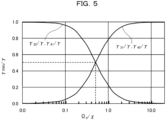
- FIG. 5 illustrates a relationship between parameter ( ⁇ d/ ⁇ ) and ⁇ mn/ ⁇ (m is 3 or 4, and n is 1 or 2).
- the color center 220 is an NV center
- ⁇ a 2.959 ⁇ 10 11 rad/s (637 nm)
- ⁇ c ⁇ a + 10 10 (1.6 GHz)
- g 10 10 rad/s
- ⁇ 10 6 rad/s
- ⁇ d 5 ⁇ 10 5 rad/s
- ⁇ 2.4 ⁇ 10 3 rad/s.
- 637 nm is the wavelength corresponding to light emission frequency ⁇ a of the color center
- 1.6 GHz is the frequency of the resonator.
- spin-photon conversion is performed focusing on a A-type three-level system using the three levels of
- spin-photon conversion is performed focusing on the A-type three-level system using the three levels of
- the static magnetic field source 30 generates a static magnetic field that reaches the color center 220
- the microwave source 40 generates a microwave that reaches the color center 220.
- Third light 13 (inelastically scattered light) having a wavelength different from that of the first light 11 is output from the optical resonator 200 to the first waveguide 100. By observing the third light 13, the state of the color center 220 may be grasped.
- transition between ground and excitation levels of one of the spin levels constituting a qubit in the color center 220 which undergoes emission relaxation with respect to the first light 11 (readout light) introduced into the color center 220, is coupled to the optical resonator 200.
- relaxation rate control is performed on the three-level system formed by application of the second light 22 (external control light).
- two relaxation rates from the excitation level to the ground level in the three-level system become equal to each other, and the efficiency of spin-photon conversion may be improved. That is, conversion efficiency of information of electron spin into information of photon may be improved.
- a diamond board 210B closer to the size of the second waveguide 210 than the diamond board 210A is obtained by processing by the focused ion beam (FIB) method or the like and forming the openings 211.
- FIB focused ion beam
- the reflective film 230 is formed by the vapor deposition method or the like so as to cover an end surface of the diamond board 210B on the X2 side.
- the optical resonator 200 may be manufactured.
- the distance between the end surface of the second waveguide 210 on the X2 side and the color center 220 is 25 nm.
- the reflective film 230 is an Ag film having a thickness of 10 nm.
- the diameter of the openings 211 is 100 nm.
- the pitch of the openings 211 is 200 nm.
- the length (size in the X1-X2 direction) of the second waveguide 210 is 2000 nm.
- the width (size in the Y1-Y2 direction) of the second waveguide 210 is 280 nm.
- the height (size in the Z1-Z2 direction) of the second waveguide 210 is 120 nm.
- FIG. 11 illustrates a calculation result of electromagnetic field distribution related to the first embodiment.
- the intensity of an electromagnetic field is standardized.
- the horizontal axis in FIG. 11 indicates a position with the X2 side being positive.
- the vertical axis in FIG. 11 indicates a position with the Y1 side being positive.
- the reflective film 230 since the reflective film 230 is provided, release of energy to the X2 side of the reflective film 230 is suppressed. Further, a standing wave having a relatively high electromagnetic field intensity is formed at the position of the color center 220.
- FIG. 11 illustrates a standing wave having a relatively high electromagnetic field intensity is formed at the position of the color center 220.
- FIG. 12 illustrates an intensity profile of a standing wave extracted in the vicinity of the color center 220.
- the value of Q of the optical resonator 200 estimated from the intensity profile illustrated in FIG. 12 is 520. This indicates that highly efficient spin-photon conversion is performed. In general, if the value of Q is about 500, on-demand (deterministic) generation of photons is possible. Therefore, this calculation result of electromagnetic field distribution suggests that on-demand (deterministic) generation of photons is possible with the quantum device 1 according to the first embodiment.
- the color center 320 is an NV center, an SiV center, a GeV center, an SnV center, a PbV center, or a BV center.
- openings are not formed in the second waveguide 310.
- the ring resonator 340 includes diamond.
- the ring resonator 340 is made of diamond.
- the ring resonator 340 is coupled to a portion of the second waveguide 310 where the color center 320 is provided.
- the electromagnetic field distribution of eigenmode in the ring resonator 340 is reflected in the second waveguide 310, and the electromagnetic field intensity increases in the vicinity of the color center 320. Consequently, the interaction between the color center 320 and the electromagnetic field is enhanced. That is, absorption and emission of light by the color center 320 are enhanced. Also, by the second embodiment, as with the first embodiment, conversion efficiency of information of electron spin into information of photon may be improved.
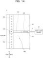
- FIG. 14 is a plan view illustrating a quantum device according to the third embodiment.
- the second waveguide 410 includes diamond including a color center 420.
- the second waveguide 410 is made of diamond including the color center 420.
- the color center 420 is provided at an end portion of the second waveguide 410 on the X2 side.
- the color center 420 is provided at a position away from an end surface of the second waveguide 410 on the X2 side toward the X1 side by about several 10 nm.
- the color center 420 is over the optical axis 29 (see FIG. 2 ). Therefore, the color center 420 is irradiated with the second light 22 emitted by the second light source 20.
- the color center 420 is an NV center, an SiV center, a GeV center, an SnV center, a PbV center, or a BV center.
- openings are not formed in the second waveguide 410.
- the third waveguide 450 includes diamond.
- the third waveguide 450 is made of diamond.
- the third waveguide 450 is orthogonal to the second waveguide 410 in a T-shape.
- the third waveguide 450 includes a portion extending from the intersection with the second waveguide 410 toward the Y1 side and a portion extending toward the Y2 side.
- the color center 420 may also be included in the third waveguide 450.
- a plurality of openings 451 arranged in the Z1-Z2 direction is formed at equal intervals.
- the openings 451 penetrate the third waveguide 450 in the Z1-Z2 direction.
- the openings 451 function as a mirror.
- the electromagnetic field distribution of eigenmode in the third waveguide 450 is reflected in the second waveguide 410, and the electromagnetic field intensity increases in the vicinity of the color center 420. Consequently, the interaction between the color center 420 and the electromagnetic field is enhanced. That is, absorption and emission of light by the color center 420 are enhanced. Also, by the third embodiment, as with the first embodiment, conversion efficiency of information of electron spin into information of photon may be improved.
- FIG. 15 is a diagram illustrating a quantum computation apparatus according to the fourth embodiment.
- a quantum computation apparatus 4 includes one beam splitter 67, two detectors 68, two wavelength filters 66, and two multiplexers 65.
- One ends of four waveguides 73 are coupled to each multiplexer 65, a half mirror 64 is provided at the other ends of the waveguides 73, and one end of a waveguide 72 is coupled to the half mirror 64.
- a waveguide 71 is coupled to the other end of the waveguide 72 in a T-shape.
- a first light source 61 is coupled to one end of the waveguide 71, and an optical resonator 62 is coupled to the other end.
- a dielectric mirror 63 is provided at the intersection between the waveguide 71 and the waveguide 72.
- the first light source 10 is used as the first light source 61.
- the optical resonator 200, 300, or 400 is used as the optical resonator 62.
- the second light source 20, the static magnetic field source 30, and the microwave source 40 are provided below the optical resonator 62.
- the first waveguide 100 is used as the waveguide 71.
- the structures of the first, second, or third embodiment are arranged in parallel.
- the third light (photon) output from one multiplexer 65 and the third light (photon) output from the other multiplexer 65 are correlated by the beam splitter 67.
- an entangled state between qubits may be formed through the photons.
- a combination of arbitrary gate operation of one qubit and two qubit gate operation enables universal quantum computation. Therefore, according to the present embodiment, a general-purpose type quantum computer using a color center of diamond may be configured.
Landscapes
- Physics & Mathematics (AREA)
- Nonlinear Science (AREA)
- General Physics & Mathematics (AREA)
- Optics & Photonics (AREA)
- Optical Integrated Circuits (AREA)
- Optical Modulation, Optical Deflection, Nonlinear Optics, Optical Demodulation, Optical Logic Elements (AREA)
Abstract
Description
- The embodiments discussed herein are related to a quantum device and a method for manufacturing a quantum device.
- In recent years, research and development of quantum computers have been vigorously advanced. For example, a quantum computer that uses a level of an electron spin of a color center of diamond as a qubit is known. In such quantum computer, information of electron spin is converted into information of photon, and optical reading is performed.
- Optical transition used for reading a state occurs probabilistically based on the selection rule of quantum mechanics. Consequently, it is difficult for a conventional quantum device used in a quantum computer to convert information of electron spin into information of photon with high efficiency.
- An object of the present disclosure is to provide a quantum device capable of improving conversion efficiency of information of electron spin into information of photon, and a method for manufacturing a quantum device.
- According to an aspect of the present disclosure, there is provided a quantum device including a first waveguide, an optical resonator that is coupled to the first waveguide, a first light source that introduces first light into the first waveguide, and a second light source that irradiates the optical resonator with second light, in which the optical resonator includes a second waveguide extending in a first direction and a color center provided in the second waveguide, the second light source has an optical axis in a second direction perpendicular to the first direction, and the color center is irradiated with the second light.
- According to the present disclosure, conversion efficiency of information of electron spin into information of photon may be improved.
- The object and advantages of the invention will be realized and attained by means of the elements and combinations particularly pointed out in the claims.
- It is to be understood that both the foregoing general description and the following detailed description are exemplary and explanatory and are not restrictive of the invention.
-
-
FIG. 1 is a plan view illustrating a quantum device according to a first embodiment. -
FIG. 2 is a cross-sectional view illustrating the quantum device according to the first embodiment. -
FIG. 3 is a diagram illustrating an example of the operation of the quantum device according to the first embodiment. -
FIG. 4 is a diagram illustrating another example of the operation of the quantum device according to the first embodiment. -
FIG. 5 is a diagram illustrating a relationship between parameter (Ωd/χ) and γmn/γ (m is 3 or 4, and n is 1 or 2). -
FIG. 6 is a perspective view illustrating a method for manufacturing an optical resonator in the quantum device according to the first embodiment (part 1). -
FIG. 7 is a perspective view illustrating the method for manufacturing an optical resonator in the quantum device according to the first embodiment (part 2). -
FIG. 8 is a perspective view illustrating the method for manufacturing an optical resonator in the quantum device according to the first embodiment (part 3). -
FIG. 9 is a perspective view illustrating the method for manufacturing an optical resonator in the quantum device according to the first embodiment (part 4). -
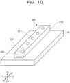
FIG. 10 is a perspective view illustrating the method for manufacturing an optical resonator in the quantum device according to the first embodiment (part 5). -
FIG. 11 is a diagram illustrating a calculation result of electromagnetic field distribution related to the first embodiment. -
FIG. 12 is a diagram illustrating an intensity profile of a standing wave extracted in the vicinity of a color center. -
FIG. 13 is a plan view illustrating a quantum device according to a second embodiment. -
FIG. 14 is a plan view illustrating a quantum device according to a third embodiment. -
FIG. 15 is a diagram illustrating a quantum computation apparatus according to a fourth embodiment. - Hereinafter, embodiments of the present disclosure will be specifically described with reference to the attached drawings. Note that, in the present specification and drawings, redundant description may be omitted by giving the same reference sign for constituent elements having substantially the same functional configuration. In the present disclosure, an X1-X2 direction, a Y1-Y2 direction, and a Z1-Z2 direction are directions orthogonal to one another. A plane including the X1-X2 direction and the Y1-Y2 direction is described as an XY plane, a plane including the Y1-Y2 direction and the Z1-Z2 direction is described as a YZ plane, and a plane including the Z1-Z2 direction and the X1-X2 direction is described as a ZX plane. Note that, for convenience, the Z1-Z2 direction is an up-down direction, a Z1 side is an upper side, and a Z2 side is a lower side. Further, a plan view refers to viewing a target object from the Z1 side, and a planar shape refers to the shape of a target object as viewed from the Z1 side.
- A first embodiment will be described.
FIG. 1 is a plan view illustrating a quantum device according to the first embodiment.FIG. 2 is a cross-sectional view illustrating the quantum device according to the first embodiment.FIG. 2 corresponds to a cross-sectional view along line I-I inFIG. 1 . - A
quantum device 1 according to the first embodiment mainly includes afirst waveguide 100, anoptical resonator 200, afirst light source 10, asecond light source 20, a static magnetic field source 30, and amicrowave source 40. Thesecond light source 20 is provided in a printedwiring board 91, the static magnetic field source 30 is provided in a printedwiring board 92, and themicrowave source 40 is provided in a printedwiring board 93. - The printed
wiring board 92 is provided over the printedwiring board 91, and the printedwiring board 93 is provided over the printedwiring board 92. The static magnetic field source 30 is positioned above thesecond light source 20, and themicrowave source 40 is positioned above the static magnetic field source 30. Thesecond light source 20, the static magnetic field source 30, and themicrowave source 40 overlap each other in the Z1-Z2 direction. Thesecond light source 20 has anoptical axis 29 in the Z1-Z2 direction. For example, thesecond light source 20 is a coherent light source. The Z1-Z2 direction is an example of a second direction. The stacking order of the printedwiring boards - A
board 50 is provided over the printedwiring board 93, and thefirst waveguide 100 and theoptical resonator 200 are provided over theboard 50. Theboard 50 supports thefirst waveguide 100 and theoptical resonator 200. The refractive index of the material of theboard 50 is lower than the refractive index of diamond. For example, the material of theboard 50 is silicon oxide (SiO2) or sapphire. - The
optical resonator 200 includes asecond waveguide 210 extending in the X1-X2 direction. Thesecond waveguide 210 includes diamond including acolor center 220. For example, thesecond waveguide 210 is made of diamond including thecolor center 220. Thecolor center 220 is provided at an end portion of thesecond waveguide 210 on the X2 side. For example, thecolor center 220 is provided at a position away from an end surface of thesecond waveguide 210 on the X2 side toward the X1 side by about several 10 nm. Thecolor center 220 is over theoptical axis 29. Therefore, thecolor center 220 is irradiated withsecond light 22 emitted by thesecond light source 20. For example, thecolor center 220 is a nitrogen-vacancy center (NV center) composed of nitrogen and a vacancy. Thecolor center 220 may be a silicon-vacancy center (SiV center) composed of silicon and vacancies, a germanium-vacancy center (GeV center) composed of germanium and vacancies, a tin-vacancy center (SnV center) composed of tin and vacancies, a lead-vacancy center (PbV center) composed of lead and vacancies, or a boron-vacancy center (BV center) composed of boron and a vacancy. Theboard 50 is an example of a support. The X1-X2 direction is an example of a first direction. - In the
second waveguide 210, a plurality ofopenings 211 arranged in the X1-X2 direction is formed at equal intervals. Theopenings 211 penetrate thesecond waveguide 210 in the Z1-Z2 direction. Theopenings 211 function as a mirror. Further, theoptical resonator 200 includes areflective film 230 that covers the end surface of thesecond waveguide 210 on the X2 side. Thereflective film 230 is a metal film having a high reflectance with respect to visible light. For example, thereflective film 230 is an Ag film having a thickness of about several 10 nm. Thereflective film 230 suppresses emission of light in theoptical resonator 200 from the end surface on the X2 side. - The
first waveguide 100 is coupled to an end portion of thesecond waveguide 210 on the X1 side. Thefirst waveguide 100 extends in the X1-X2 direction. Thefirst waveguide 100 includes a nitride semiconductor, for example, AIN, which has a lower refractive index and a lower absorptance in the visible light range than diamond. For example, thefirst waveguide 100 is made of AIN. Thefirst light source 10 irradiates thefirst waveguide 100 withfirst light 11. For example, thefirst light source 10 is a quantum light source. - In the present embodiment, the following relationship holds. Coupling coefficient g of the
optical resonator 200 is smaller than the absolute value of a difference between resonance frequency wc of theoptical resonator 200 and light emission frequency ωa of the color center 220 (|ωc - ωa|). Frequency ωd of thesecond light 22 is equal to ωa - 2χ. Here, χ is g2/(ωc - ωa). - Next, the operation of the
quantum device 1 according to the first embodiment will be described.FIG. 3 is a diagram illustrating an example of the operation of thequantum device 1 according to the first embodiment.FIG. 4 is a diagram illustrating another example of the operation of thequantum device 1 according to the first embodiment. - In the
quantum device 1, thefirst light 11 is introduced from thefirst light source 10 into thefirst waveguide 100, and thefirst light 11 reaches thecolor center 220. Thecolor center 220 forms, in the band gap, a spin level (spin triplet) that is energetically discretized at a frequency of the order of GHz corresponding to the spinquantum number 1 of itself. In this case, when a spin level of which spin magnetic quantum number is 0 and a spin level of which spin magnetic quantum number is -1 are regarded as qubits,spin 0 indicates a light absorption-emission process between ground and excitation levels in the visible light range, that is, a process of emission relaxation. On the other hand, spin -1 indicates a process of non-emission relaxation to the ground level ofspin 0 through a metastable state (spin singlet) ofspin 0. That is, by measuring photon information (the presence or absence of photon emission) emitted after optical excitation within a time scale in which the coherence of a state is held after state operation by a microwave to a qubit level, reading of a qubit through a photon (spin-photon conversion) may be performed. - Further, with respect to transition between ground and excitation levels for emission relaxation, two systems of two-level systems represented by four levels of |g, 0>, |g, 1>, |e, 0>, and |e, 1> are formed based on the Jaynes-Cummings model. Here, g represents a ground level of emission relaxation, e represents an excitation level of emission relaxation, and 0 or 1 represents the number of photons in the
optical resonator 200. With the second light 22 (external control light), these two systems of two-level systems form dressed levels including four levels of |1>, |2>, |3>, and |4> as illustrated inFIG. 3 andFIG. 4 . The two levels |1> and |2> are levels of thecolor center 220 itself, and |3> and |4> are levels formed by irradiation with thesecond light 22. Here, the relaxation rate from the level |4> to the level |1> is γ41, the relaxation rate from the level |4> to the level |2> is γ42, the relaxation rate from the level |3> to the level |1> is γ31, and the relaxation rate from the level |3> to the level |2> is γ32. In this case, γ = γ31 + γ32 =γ41 + γ42 holds. When the intensity of thesecond light 22 is Ωd, γ31, γ32, γ41, and γ42 are represented as follows.

-
FIG. 5 illustrates a relationship between parameter (Ωd/χ) and γmn/γ (m is 3 or 4, and n is 1 or 2). Here, assuming that thecolor center 220 is an NV center, ωa = 2.959 × 10¹¹ rad/s (637 nm), ωc = ωa + 1010 (1.6 GHz), g = 1010 rad/s, χ = 106 rad/s, Ωd =5 × 10⁵ rad/s, and γ = 2.4 × 10³ rad/s. 637 nm is the wavelength corresponding to light emission frequency ωa of the color center, and 1.6 GHz is the frequency of the resonator. As illustrated inFIG. 5 , when parameter (Ωd/X) is 0.5, γ31/γ, γ32/γ, γ41/γ, and γ42/γ are equal to each other. That is, when parameter (Ωd/χ) is 0.5, at least relaxation rate γ31 and relaxation rate γ32 are equal to each other, or relaxation rate γ41 and relaxation rate γ42 are equal to each other. Further, when coupling coefficient g and volume gωcVm of theoptical resonator 200 are taken into consideration, the value of Q represented by (2g2/kγ) × (4π2/3λ3) × Vm is about 500. This indicates that highly efficient spin-photon conversion is performed. Ultimately, on-demand (deterministic) optical spin-photon conversion may be possible. Note that k and λ represent a relaxation rate and a resonance wavelength of the resonator, respectively. - In the present embodiment, in the example illustrated in
FIG. 3 , spin-photon conversion is performed focusing on a A-type three-level system using the three levels of |1>, |2>, and |4> without using the level |3>. Further, in the example illustrated inFIG. 4 , spin-photon conversion is performed focusing on the A-type three-level system using the three levels of |1>, |2>, and |3> without using the level |4>. When spin-photon conversion is performed, the static magnetic field source 30 generates a static magnetic field that reaches thecolor center 220, and themicrowave source 40 generates a microwave that reaches thecolor center 220. Third light 13 (inelastically scattered light) having a wavelength different from that of thefirst light 11 is output from theoptical resonator 200 to thefirst waveguide 100. By observing thethird light 13, the state of thecolor center 220 may be grasped. - As described above, in the first embodiment, transition between ground and excitation levels of one of the spin levels constituting a qubit in the
color center 220, which undergoes emission relaxation with respect to the first light 11 (readout light) introduced into thecolor center 220, is coupled to theoptical resonator 200. Further, relaxation rate control is performed on the three-level system formed by application of the second light 22 (external control light). As a result, two relaxation rates from the excitation level to the ground level in the three-level system become equal to each other, and the efficiency of spin-photon conversion may be improved. That is, conversion efficiency of information of electron spin into information of photon may be improved. - Next, a method for manufacturing the
optical resonator 200 will be described.FIG. 6 to FIG. 10 are perspective views illustrating the method for manufacturing theoptical resonator 200 in thequantum device 1 according to the first embodiment. - First, as illustrated in
FIG. 6 , athin diamond board 210A serving as a base member of thesecond waveguide 210 is prepared, and thediamond board 210A is cleaned. Next, thecolor center 220 is formed by implanting a desired element species, for example, nitrogen by the ion implantation method or the like and performing annealing (activation treatment). - Thereafter, as illustrated in
FIG. 7 , adiamond board 210B closer to the size of thesecond waveguide 210 than thediamond board 210A is obtained by processing by the focused ion beam (FIB) method or the like and forming theopenings 211. - Subsequently, as illustrated in
FIG. 8 , thereflective film 230 is formed by the vapor deposition method or the like so as to cover an end surface of thediamond board 210B on the X2 side. - Next, as illustrated in
FIG. 9 , thediamond board 210B is processed by FIB or the like, and thesecond waveguide 210 is obtained. - Thereafter, as illustrated in
FIG. 10 , thesecond waveguide 210 is bonded over theboard 50. For example, thefirst waveguide 100 is formed over theboard 50 in advance. - In this way, the
optical resonator 200 may be manufactured. - When the
quantum device 1 is manufactured, the printedwiring board 91 including the secondlight source 20, the printedwiring board 92 including the static magnetic field source 30, and the printedwiring board 93 including themicrowave source 40 are stacked. Then, theboard 50 provided with thefirst waveguide 100 and the optical resonator 200 (seeFIG. 10 ) is provided over the printedwiring board 93. Thefirst light source 10 may be coupled to thefirst waveguide 100 in advance, or may be coupled to thefirst waveguide 100 after theboard 50 is provided over the printedwiring board 93. - Here, a calculation result of electromagnetic field distribution related to the first embodiment will be described. In this calculation, assuming that the
color center 220 is an NV center, electromagnetic field distribution in theoptical resonator 200 under the following sizes (structural parameters) was obtained. - The distance between the end surface of the
second waveguide 210 on the X2 side and thecolor center 220 is 25 nm. Thereflective film 230 is an Ag film having a thickness of 10 nm. The diameter of theopenings 211 is 100 nm. The pitch of theopenings 211 is 200 nm. The length (size in the X1-X2 direction) of thesecond waveguide 210 is 2000 nm. The width (size in the Y1-Y2 direction) of thesecond waveguide 210 is 280 nm. The height (size in the Z1-Z2 direction) of thesecond waveguide 210 is 120 nm. -
FIG. 11 illustrates a calculation result of electromagnetic field distribution related to the first embodiment. The intensity of an electromagnetic field is standardized. With reference to an end surface of theoptical resonator 200 on the X1 side, the horizontal axis inFIG. 11 indicates a position with the X2 side being positive. With reference to the center of theoptical resonator 200 in the Y1-Y2 direction, the vertical axis inFIG. 11 indicates a position with the Y1 side being positive. As illustrated inFIG. 11 , since thereflective film 230 is provided, release of energy to the X2 side of thereflective film 230 is suppressed. Further, a standing wave having a relatively high electromagnetic field intensity is formed at the position of thecolor center 220.FIG. 12 illustrates an intensity profile of a standing wave extracted in the vicinity of thecolor center 220. The value of Q of theoptical resonator 200 estimated from the intensity profile illustrated inFIG. 12 is 520. This indicates that highly efficient spin-photon conversion is performed. In general, if the value of Q is about 500, on-demand (deterministic) generation of photons is possible. Therefore, this calculation result of electromagnetic field distribution suggests that on-demand (deterministic) generation of photons is possible with thequantum device 1 according to the first embodiment. - A second embodiment will be described.
FIG. 13 is a plan view illustrating a quantum device according to the second embodiment. - A
quantum device 2 according to the second embodiment includes anoptical resonator 300 instead of theoptical resonator 200. Theoptical resonator 300 includes asecond waveguide 310 extending in the X1-X2 direction and aring resonator 340. - As with the
second waveguide 210, thesecond waveguide 310 includes diamond including acolor center 320. For example, thesecond waveguide 310 is made of diamond including thecolor center 320. Thecolor center 320 is provided at an end portion of thesecond waveguide 310 on the X2 side. For example, thecolor center 320 is provided at a position away from an end surface of thesecond waveguide 310 on the X2 side toward the X1 side by about several 10 nm. As with thecolor center 220, thecolor center 320 is over the optical axis 29 (seeFIG. 2 ). Therefore, thecolor center 320 is irradiated with the second light 22 emitted by the secondlight source 20. For example, thecolor center 320 is an NV center, an SiV center, a GeV center, an SnV center, a PbV center, or a BV center. Unlike thesecond waveguide 210, openings are not formed in thesecond waveguide 310. - The
ring resonator 340 includes diamond. For example, thering resonator 340 is made of diamond. Thering resonator 340 is coupled to a portion of thesecond waveguide 310 where thecolor center 320 is provided. - Other configurations are similar to those of the first embodiment.
- In the second embodiment, the electromagnetic field distribution of eigenmode in the
ring resonator 340 is reflected in thesecond waveguide 310, and the electromagnetic field intensity increases in the vicinity of thecolor center 320. Consequently, the interaction between thecolor center 320 and the electromagnetic field is enhanced. That is, absorption and emission of light by thecolor center 320 are enhanced. Also, by the second embodiment, as with the first embodiment, conversion efficiency of information of electron spin into information of photon may be improved. - A third embodiment will be described.
FIG. 14 is a plan view illustrating a quantum device according to the third embodiment. - A
quantum device 3 according to the third embodiment includes anoptical resonator 400 instead of theoptical resonator 200. Theoptical resonator 400 includes asecond waveguide 410 extending in the X1-X2 direction and athird waveguide 450 extending in the Y1-Y2 direction. - As with the
second waveguide 210, thesecond waveguide 410 includes diamond including acolor center 420. For example, thesecond waveguide 410 is made of diamond including thecolor center 420. Thecolor center 420 is provided at an end portion of thesecond waveguide 410 on the X2 side. For example, thecolor center 420 is provided at a position away from an end surface of thesecond waveguide 410 on the X2 side toward the X1 side by about several 10 nm. As with thecolor center 220, thecolor center 420 is over the optical axis 29 (seeFIG. 2 ). Therefore, thecolor center 420 is irradiated with the second light 22 emitted by the secondlight source 20. For example, thecolor center 420 is an NV center, an SiV center, a GeV center, an SnV center, a PbV center, or a BV center. Unlike thesecond waveguide 210, openings are not formed in thesecond waveguide 410. - The
third waveguide 450 includes diamond. For example, thethird waveguide 450 is made of diamond. Thethird waveguide 450 is orthogonal to thesecond waveguide 410 in a T-shape. Thethird waveguide 450 includes a portion extending from the intersection with thesecond waveguide 410 toward the Y1 side and a portion extending toward the Y2 side. Thecolor center 420 may also be included in thethird waveguide 450. In thethird waveguide 450, a plurality ofopenings 451 arranged in the Z1-Z2 direction is formed at equal intervals. Theopenings 451 penetrate thethird waveguide 450 in the Z1-Z2 direction. Theopenings 451 function as a mirror. - Other configurations are similar to those of the first embodiment.
- In the third embodiment, the electromagnetic field distribution of eigenmode in the
third waveguide 450 is reflected in thesecond waveguide 410, and the electromagnetic field intensity increases in the vicinity of thecolor center 420. Consequently, the interaction between thecolor center 420 and the electromagnetic field is enhanced. That is, absorption and emission of light by thecolor center 420 are enhanced. Also, by the third embodiment, as with the first embodiment, conversion efficiency of information of electron spin into information of photon may be improved. - A fourth embodiment will be described.
FIG. 15 is a diagram illustrating a quantum computation apparatus according to the fourth embodiment. - A
quantum computation apparatus 4 according to the fourth embodiment includes onebeam splitter 67, twodetectors 68, twowavelength filters 66, and twomultiplexers 65. One ends of fourwaveguides 73 are coupled to eachmultiplexer 65, ahalf mirror 64 is provided at the other ends of thewaveguides 73, and one end of awaveguide 72 is coupled to thehalf mirror 64. Awaveguide 71 is coupled to the other end of thewaveguide 72 in a T-shape. Afirst light source 61 is coupled to one end of thewaveguide 71, and anoptical resonator 62 is coupled to the other end. Adielectric mirror 63 is provided at the intersection between thewaveguide 71 and thewaveguide 72. For example, thefirst light source 10 is used as thefirst light source 61. For example, theoptical resonator optical resonator 62. Although illustration is omitted, as with the first, second, or third embodiment, the secondlight source 20, the static magnetic field source 30, and themicrowave source 40 are provided below theoptical resonator 62. For example, thefirst waveguide 100 is used as thewaveguide 71. - As described above, in the fourth embodiment, the structures of the first, second, or third embodiment are arranged in parallel.
- When one qubit operation is performed, after the state operation on a color center (qubit) by a microwave, first light (readout light) is incident on the
optical resonator 62 through thedielectric mirror 63. Further, the color center is irradiated with second light from a second light source. The first light is reflected by theoptical resonator 62, and third light (photon) is output. The third light (photon) is reflected by thedielectric mirror 63 toward thewaveguide 72, and is detected by thedetector 68 through thehalf mirror 64, thewaveguide 73, themultiplexer 65, thewavelength filter 66, and thebeam splitter 67. - When two qubit operation is performed, the third light (photon) output from one
multiplexer 65 and the third light (photon) output from theother multiplexer 65 are correlated by thebeam splitter 67. By observing the two photons with the detectors, an entangled state between qubits may be formed through the photons. - As described above, a combination of arbitrary gate operation of one qubit and two qubit gate operation enables universal quantum computation. Therefore, according to the present embodiment, a general-purpose type quantum computer using a color center of diamond may be configured.
- Although the preferred embodiments and the like have been described in detail above, the present disclosure is not limited to the embodiments and the like described above. Various modifications and replacements may be made to the embodiments and the like described above without departing from the scope of the claims.
-
- PTL 1:
Japanese Laid-open Patent Publication No. 2014-216596 - PTL 2: International Publication Pamphlet No.
WO 2020/203746 - NPL 1: Kazuki Koshino and three others, "Deterministic Quantum State Switching by Single Photon", Journal of the Physical Society of Japan, Vol. 1, No. 1, 2014
-
- 1, 2, 3 Quantum device
- 4 Quantum computation apparatus
- 10, 61 First light source
- 11 First light
- 13 Third light
- 20 Second light source
- 22 Second light
- 29 Optical axis
- 30 Static magnetic field source
- 40 Microwave source
- 50 Board
- 62, 200, 300, 400 Optical resonator
- 71, 72, 73 Waveguide
- 100 First waveguide
- 210, 310, 410 Second waveguide
- 211, 451 Opening
- 220, 320, 420 Color center
- 230 Reflective film
- 340 Ring resonator
- 450 Third waveguide
Claims (15)
- A quantum device comprising:a first waveguide;an optical resonator that is coupled to the first waveguide;a first light source that introduces first light into the first waveguide; anda second light source that irradiates the optical resonator with second light,whereinthe optical resonator includes a second waveguide that extends in a first direction and a color center that is provided in the second waveguide,the second light source has an optical axis in a second direction perpendicular to the first direction, andthe color center is irradiated with the second light.
- The quantum device according to claim 1, wherein third light of which wavelength is different from that of the first light is output from the optical resonator to the first waveguide.
- The quantum device according to claim 1, whereinthe color center is provided at one end portion of the second waveguide, andthe first waveguide is coupled to the other end portion of the second waveguide.
- The quantum device according to claim 1 or 2, wherein the device includesa static magnetic field source that generates a magnetic field that reaches the color center, anda microwave source that generates a microwave that reaches the color center.
- The quantum device according to claim 1 or 2, wherein the color center includes a composite defect of N, Si, Ge, Sn, or Pb, or arbitrary combination thereof, and a vacancy.
- The quantum device according to claim 1 or 2, wherein material of the second waveguide is diamond, and a refractive index of material of the first waveguide is lower than a refractive index of diamond.
- The quantum device according to claim 1 or 2, whereinthe first light source is a quantum light source, andthe second light source is a coherent light source.
- The quantum device according to claim 1 or 2, wherein a plurality of openings arranged in the first direction is formed at equal intervals in the second waveguide.
- The quantum device according to claim 1 or 2, wherein a coupling coefficient of the optical resonator is smaller than an absolute value of a difference between a resonance frequency of the optical resonator and a light emission frequency of the color center.
- The quantum device according to claim 1 or 2, whereinthe first light source is a coherent light source, andwhen a light intensity of the second light source is Ωd, a coupling coefficient of the optical resonator is g, a resonance frequency of the optical resonator is ωc, and a light emission frequency of the color center is ωa,
 and
and
- The quantum device according to claim 10, wherein a frequency of the second light is equal to ωa - 2χ.
- The quantum device according to claim 1 or 2, wherein the device includes a support that supports the first waveguide and the optical resonator.
- The quantum device according to claim 12, wherein a refractive index of material of the support is lower than a refractive index of diamond.
- A method for manufacturing a quantum device comprising:a step of providing an optical resonator that is coupled to a first waveguide;a step of providing a first light source that introduces first light into the first waveguide; anda step of providing a second light source that irradiates the optical resonator with second light,whereinthe optical resonator includes a second waveguide that extends in a first direction and a color center that is provided in the second waveguide, andthe second light source has an optical axis in a second direction perpendicular to the first direction, and is disposed such that the color center is irradiated with the second light.
- A quantum computation apparatus comprising the quantum device according to claim 1 or 2.
Applications Claiming Priority (1)
| Application Number | Priority Date | Filing Date | Title |
|---|---|---|---|
| PCT/JP2022/021961 WO2023233473A1 (en) | 2022-05-30 | 2022-05-30 | Quantum device and method for manufacturing quantum device |
Publications (2)
| Publication Number | Publication Date |
|---|---|
| EP4535428A1 true EP4535428A1 (en) | 2025-04-09 |
| EP4535428A4 EP4535428A4 (en) | 2025-07-09 |
Family
ID=89025906
Family Applications (1)
| Application Number | Title | Priority Date | Filing Date |
|---|---|---|---|
| EP22944762.8A Pending EP4535428A4 (en) | 2022-05-30 | 2022-05-30 | QUANTUM DEVICE AND METHOD FOR MANUFACTURING A QUANTUM DEVICE |
Country Status (4)
| Country | Link |
|---|---|
| US (1) | US20260126590A1 (en) |
| EP (1) | EP4535428A4 (en) |
| JP (1) | JPWO2023233473A1 (en) |
| WO (1) | WO2023233473A1 (en) |
Families Citing this family (1)
| Publication number | Priority date | Publication date | Assignee | Title |
|---|---|---|---|---|
| WO2025186860A1 (en) * | 2024-03-04 | 2025-09-12 | Fujitsu Limited | Optical waveguide and method of manufacturing optical waveguide |
Family Cites Families (6)
| Publication number | Priority date | Publication date | Assignee | Title |
|---|---|---|---|---|
| US8837544B2 (en) * | 2011-10-28 | 2014-09-16 | Hewlett-Packard Development Company, L.P. | Quantum optical device |
| JP6066314B2 (en) | 2013-04-30 | 2017-01-25 | 日本電信電話株式会社 | How to configure qubits |
| TWI619671B (en) * | 2014-06-26 | 2018-04-01 | 麻省理工學院 | Methods and apparatus for nanofabrication using a pliable membrane mask |
| US11054590B1 (en) * | 2019-03-05 | 2021-07-06 | Massachusetts Institute Of Technology | Scalable integration of hybrid optoelectronic and quantum optical systems into photonic circuits |
| WO2020203746A1 (en) | 2019-04-02 | 2020-10-08 | ローム株式会社 | Single photon source and method for outputting single photon |
| EP4224376A4 (en) * | 2020-09-30 | 2023-11-22 | Fujitsu Limited | QUANTUM CIRCUIT, QUANTUM COMPUTER AND METHOD FOR PRODUCING QUANTUM CIRCUIT |
-
2022
- 2022-05-30 WO PCT/JP2022/021961 patent/WO2023233473A1/en not_active Ceased
- 2022-05-30 EP EP22944762.8A patent/EP4535428A4/en active Pending
- 2022-05-30 JP JP2024524534A patent/JPWO2023233473A1/ja active Pending
-
2024
- 2024-11-18 US US18/950,250 patent/US20260126590A1/en active Pending
Also Published As
| Publication number | Publication date |
|---|---|
| EP4535428A4 (en) | 2025-07-09 |
| JPWO2023233473A1 (en) | 2023-12-07 |
| US20260126590A1 (en) | 2026-05-07 |
| WO2023233473A1 (en) | 2023-12-07 |
Similar Documents
| Publication | Publication Date | Title |
|---|---|---|
| Masson et al. | Universality of Dicke superradiance in arrays of quantum emitters | |
| Ollivier et al. | Reproducibility of high-performance quantum dot single-photon sources | |
| US9157859B2 (en) | Efficient fluorescence detection in solid state spin systems | |
| US20210224678A1 (en) | Scalable Integration of Hybrid Optoelectronic and Quantum Optical Systems into Photonic Circuits | |
| Hong et al. | Experimental methods for trapping ions using microfabricated surface ion traps | |
| Myroshnychenko et al. | Unveiling and imaging degenerate states in plasmonic nanoparticles with nanometer resolution | |
| US20230369004A1 (en) | X-ray radiation source system and method for design of the same | |
| US20260126590A1 (en) | Quantum device and method for manufacturing quantum device | |
| JP2020519897A (en) | Frequency conversion device and method | |
| Abudayyeh et al. | Overcoming the rate-directionality trade-off: a room-temperature ultrabright quantum light source | |
| Canet-Ferrer et al. | Purcell effect in photonic crystal microcavities embedding InAs/InP quantum wires | |
| Christinck et al. | Bright single-photon emission from a GeV center in diamond under a microfabricated solid immersion lens at room temperature | |
| Fiedler et al. | Disentangling cathodoluminescence spectra in nanophotonics: particle eigenmodes vs transition radiation | |
| US10879669B2 (en) | Photonic crystal laser | |
| Grishina et al. | X-ray imaging of functional three-dimensional nanostructures on massive substrates | |
| Vaskin et al. | Manipulation of quantum dot emission with semiconductor metasurfaces exhibiting magnetic quadrupole resonances | |
| Bremer et al. | Cesium‐vapor‐based delay of single photons emitted by deterministically fabricated quantum dot microlenses | |
| Jaworski et al. | Xenon plasma-focused ion beam milling for fabrication of high-purity, bright single-photon sources operating in the C-band | |
| Jeon et al. | Diamond photonic crystal mirror with a partial bandgap by two 2D photonic crystal layers | |
| McGehee et al. | Two-dimensional imaging and modification of nanophotonic resonator modes using a focused ion beam | |
| Tsukanov | Quantum dots in photonic molecules and quantum informatics. Part I | |
| Coenen | Angle-resolved cathodoluminescence nanoscopy | |
| Dey et al. | Culling a self-assembled quantum dot as a single-photon source using X-ray microscopy | |
| Gough et al. | Faraday-cage-assisted etching of suspended gallium nitride nanostructures | |
| Geng | Defect Quantum Emitters in Gallium Nitride |
Legal Events
| Date | Code | Title | Description |
|---|---|---|---|
| STAA | Information on the status of an ep patent application or granted ep patent |
Free format text: STATUS: THE INTERNATIONAL PUBLICATION HAS BEEN MADE |
|
| PUAI | Public reference made under article 153(3) epc to a published international application that has entered the european phase |
Free format text: ORIGINAL CODE: 0009012 |
|
| STAA | Information on the status of an ep patent application or granted ep patent |
Free format text: STATUS: REQUEST FOR EXAMINATION WAS MADE |
|
| 17P | Request for examination filed |
Effective date: 20241120 |
|
| AK | Designated contracting states |
Kind code of ref document: A1 Designated state(s): AL AT BE BG CH CY CZ DE DK EE ES FI FR GB GR HR HU IE IS IT LI LT LU LV MC MK MT NL NO PL PT RO RS SE SI SK SM TR |
|
| REG | Reference to a national code |
Ref country code: DE Ref legal event code: R079 Free format text: PREVIOUS MAIN CLASS: H01L0029060000 Ipc: G02F0003000000 |
|
| A4 | Supplementary search report drawn up and despatched |
Effective date: 20250610 |
|
| RIC1 | Information provided on ipc code assigned before grant |
Ipc: G06N 10/40 20220101ALI20250603BHEP Ipc: G02B 6/42 20060101ALI20250603BHEP Ipc: G02B 6/122 20060101ALI20250603BHEP Ipc: G02F 1/365 20060101ALI20250603BHEP Ipc: G02B 6/00 20060101ALI20250603BHEP Ipc: G02F 3/00 20060101AFI20250603BHEP |
|
| DAV | Request for validation of the european patent (deleted) | ||
| DAX | Request for extension of the european patent (deleted) |