EP4535426A1 - Display device using semiconductor light emitting element - Google Patents
Display device using semiconductor light emitting element Download PDFInfo
- Publication number
- EP4535426A1 EP4535426A1 EP22908809.1A EP22908809A EP4535426A1 EP 4535426 A1 EP4535426 A1 EP 4535426A1 EP 22908809 A EP22908809 A EP 22908809A EP 4535426 A1 EP4535426 A1 EP 4535426A1
- Authority
- EP
- European Patent Office
- Prior art keywords
- light
- emitting device
- arrangement
- display device
- pixel area
- Prior art date
- Legal status (The legal status is an assumption and is not a legal conclusion. Google has not performed a legal analysis and makes no representation as to the accuracy of the status listed.)
- Pending
Links
Images





Classifications
-
- H—ELECTRICITY
- H10—SEMICONDUCTOR DEVICES; ELECTRIC SOLID-STATE DEVICES NOT OTHERWISE PROVIDED FOR
- H10H—INORGANIC LIGHT-EMITTING SEMICONDUCTOR DEVICES HAVING POTENTIAL BARRIERS
- H10H20/00—Individual inorganic light-emitting semiconductor devices having potential barriers, e.g. light-emitting diodes [LED]
- H10H20/80—Constructional details
- H10H20/85—Packages
- H10H20/857—Interconnections, e.g. lead-frames, bond wires or solder balls
-
- H—ELECTRICITY
- H10—SEMICONDUCTOR DEVICES; ELECTRIC SOLID-STATE DEVICES NOT OTHERWISE PROVIDED FOR
- H10H—INORGANIC LIGHT-EMITTING SEMICONDUCTOR DEVICES HAVING POTENTIAL BARRIERS
- H10H20/00—Individual inorganic light-emitting semiconductor devices having potential barriers, e.g. light-emitting diodes [LED]
- H10H20/80—Constructional details
- H10H20/81—Bodies
- H10H20/819—Bodies characterised by their shape, e.g. curved or truncated substrates
-
- H—ELECTRICITY
- H10—SEMICONDUCTOR DEVICES; ELECTRIC SOLID-STATE DEVICES NOT OTHERWISE PROVIDED FOR
- H10H—INORGANIC LIGHT-EMITTING SEMICONDUCTOR DEVICES HAVING POTENTIAL BARRIERS
- H10H20/00—Individual inorganic light-emitting semiconductor devices having potential barriers, e.g. light-emitting diodes [LED]
- H10H20/80—Constructional details
- H10H20/81—Bodies
- H10H20/817—Bodies characterised by the crystal structures or orientations, e.g. polycrystalline, amorphous or porous
-
- H—ELECTRICITY
- H10—SEMICONDUCTOR DEVICES; ELECTRIC SOLID-STATE DEVICES NOT OTHERWISE PROVIDED FOR
- H10H—INORGANIC LIGHT-EMITTING SEMICONDUCTOR DEVICES HAVING POTENTIAL BARRIERS
- H10H20/00—Individual inorganic light-emitting semiconductor devices having potential barriers, e.g. light-emitting diodes [LED]
- H10H20/80—Constructional details
- H10H20/83—Electrodes
-
- H—ELECTRICITY
- H10—SEMICONDUCTOR DEVICES; ELECTRIC SOLID-STATE DEVICES NOT OTHERWISE PROVIDED FOR
- H10H—INORGANIC LIGHT-EMITTING SEMICONDUCTOR DEVICES HAVING POTENTIAL BARRIERS
- H10H29/00—Integrated devices, or assemblies of multiple devices, comprising at least one light-emitting semiconductor element covered by group H10H20/00
- H10H29/30—Active-matrix LED displays
- H10H29/32—Active-matrix LED displays characterised by the geometry or arrangement of elements within a subpixel, e.g. arrangement of the transistor within its RGB subpixel
-
- H—ELECTRICITY
- H10—SEMICONDUCTOR DEVICES; ELECTRIC SOLID-STATE DEVICES NOT OTHERWISE PROVIDED FOR
- H10H—INORGANIC LIGHT-EMITTING SEMICONDUCTOR DEVICES HAVING POTENTIAL BARRIERS
- H10H29/00—Integrated devices, or assemblies of multiple devices, comprising at least one light-emitting semiconductor element covered by group H10H20/00
- H10H29/30—Active-matrix LED displays
- H10H29/362—Active-matrix LED displays comprising more than three subpixels, e.g. red-green-blue-white [RGBW]
-
- H—ELECTRICITY
- H10—SEMICONDUCTOR DEVICES; ELECTRIC SOLID-STATE DEVICES NOT OTHERWISE PROVIDED FOR
- H10H—INORGANIC LIGHT-EMITTING SEMICONDUCTOR DEVICES HAVING POTENTIAL BARRIERS
- H10H29/00—Integrated devices, or assemblies of multiple devices, comprising at least one light-emitting semiconductor element covered by group H10H20/00
- H10H29/30—Active-matrix LED displays
- H10H29/49—Interconnections, e.g. wiring lines or terminals
-
- H—ELECTRICITY
- H10—SEMICONDUCTOR DEVICES; ELECTRIC SOLID-STATE DEVICES NOT OTHERWISE PROVIDED FOR
- H10W—GENERIC PACKAGES, INTERCONNECTIONS, CONNECTORS OR OTHER CONSTRUCTIONAL DETAILS OF DEVICES COVERED BY CLASS H10
- H10W90/00—Package configurations
Definitions
- LCD liquid crystal display
- OLED organic light emitting diode
- LED light emitting diode
- Sapphire which is used as a substrate on which a gallium nitride-based semiconductor is grown, has a tilted crystal surface.
- a R-plane has a crystal surface tilted along a m-axis.
- the ordinary sapphire may have the R-plane as a growth plane. Because the R-plane has a surface tilted with respect to a hexagonal prism crystal shape, the sapphire substrate and the gallium nitride-based semiconductor grown on the crystal surface of the sapphire substrate may have such a tilt angle.
- such a tilt angle may also be formed as a light-emitting device is formed as the gallium nitride-based semiconductor on the sapphire substrate and then is cut in a direction of the crystal surface of the sapphire substrate.
- an unintended parasitic capacitance may occur due to an electric field formed by a difference in polarity between a signal electrode/a common electrode of the light-emitting device.
- the corresponding effect may be accumulated by the total number of light-emitting devices used in the display device, and finally, a ghost phenomenon may appear in a unit of a display product.
- the present disclosure is to provide a display device using a semiconductor light-emitting device that may cancel the biased light distributions of the light-emitting devices caused by the crystallinity of the light-emitting devices.
- the present disclosure is to provide a display device using a semiconductor light-emitting device that may solve a problem in that, when viewing the display device from the outside, a color of a display appears differently depending on a viewing direction.
- the present disclosure is to provide a display device using a semiconductor light-emitting device that may reduce a parasitic capacitance caused by a difference in electrical polarity between the light-emitting devices.
- the present disclosure is to provide a display device using a semiconductor light-emitting device that may cancel an electric field generated by a difference in electrical polarity between the light-emitting devices.
- the present disclosure is to provide a display device using a semiconductor light-emitting device that may visually reinforce an area with weak color when viewing the display from one side to correct a color difference of the display perceived on left and right sides.
- a display device using a light-emitting device includes a wiring substrate having multiple unit pixel areas defined therein, a wiring electrode including first wiring electrodes and a second wiring electrode arranged on the wiring substrate, and each light-emitting device installed in each unit pixel area so as to be electrically connected to each first wiring electrode and the second wiring electrode to constitute each sub-pixel, and the light-emitting devices include a first light-emitting device located in a first pixel area and installed in a first arrangement, and a second light-emitting device located in a second pixel area adjacent to the first pixel area and installed in a second arrangement symmetrical to the first arrangement.
- a parasitic capacitance generated by a difference in electrical polarity between the first light-emitting device and the second light-emitting device may be reduced by the first arrangement and the second arrangement.
- positions of electrodes of the first light-emitting device and the second light-emitting device may be symmetrical to each other in the first arrangement and the second arrangement.
- the first wiring electrode corresponding to the first pixel area and an adjacent first wiring electrode corresponding to the second pixel area may be symmetrically positioned with respect to each other around a center point between the first pixel area and the second pixel area.
- the center point between the first pixel area and the second pixel area may correspond to the second wiring electrode.
- the first pixel area and the second pixel area may form a pair between the first wiring electrode and a first wiring electrode adjacent thereto.
- the first light-emitting device and the second light-emitting device may be tilted symmetrical to each other to have the same tilt angles in opposite directions by the first arrangement and the second arrangement.
- each light-emitting device may include a first-type electrode and a second-type electrode, and have an asymmetric light distribution with respect to a direction for connecting the first-type electrode and the second-type electrode to each other.
- the asymmetric light distributions may be canceled with each other by the first arrangement and the second arrangement.
- the first light-emitting device and the second light-emitting device may emit light of the same color.
- a display device using a light-emitting device includes a wiring substrate having multiple unit pixel areas defined therein, a wiring electrode including first wiring electrodes and a second wiring electrode arranged on the wiring substrate, and each light-emitting device installed in each unit pixel area so as to be electrically connected to each first wiring electrode and the second wiring electrode to constitute each sub-pixel, and the light-emitting devices include a first light-emitting device located in a first sub-pixel area and installed in a first arrangement, and a second light-emitting device located in a second sub-pixel area adjacent to the first sub-pixel area and installed in a second arrangement symmetrical to the first arrangement with respect to the first wiring electrode.
- the biased light distributions of the light-emitting devices resulting from the crystallinity of the light-emitting devices may be cancelled with each other. That is, the asymmetrical light distributions of the light-emitting devices may be canceled.
- the parasitic capacitance generated by the difference in the electrical polarity of the light-emitting devices may be reduced.
- the electric field generated by the difference in the electrical polarity between the light-emitting devices may be canceled.
- a semiconductor light-emitting device mentioned herein is a concept including an LED, a micro LED, and the like, and is able to be used interchangeably with those.
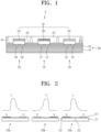
- FIG. 1 is a schematic diagram of a display device using a semiconductor light-emitting device according to an embodiment of the present disclosure.
- the first electrode pads 130, 131, and 132 may respectively correspond to the signal electrodes 121, 122, and 123, and the second electrode pads 140, 141, and 142 may correspond to the common electrode 124.
- the light-emitting devices 210, 220, and 230 may form the individual sub-pixels and be repeatedly positioned on the wiring substrate 100.
- each pixel area 101 may be repeatedly disposed on the wiring substrate 100.
- the pixel areas 101 may be repeatedly positioned along one line of the data electrodes (the first wiring electrodes) 121, 122, and 123 or line of the scan electrode (the second wiring electrode) 124 in a longitudinal direction.
- the red light-emitting device 210, the green light-emitting device 220, and the blue light-emitting device 230 may be repeatedly positioned along a left and right direction.
- a red light-emitting device of an adjacent pixel area may be positioned on a right side of the blue light-emitting device 230.
- another data electrode (first wiring electrode) line or scan electrode (second wiring electrode) line adjacent to one data electrode (first wiring electrode) line or scan electrode (second wiring electrode) line in a parallel manner may be located (see FIG. 8 ).
- a pixel area 102 (see FIG. 8 ) having the same arrangement of the light-emitting devices 210, 220, and 230 as the pixel area 101 may be located on the adjacent data electrode (first wiring electrode) line or scan electrode (second wiring electrode) line.
- light-emitting devices having the same color may be located adjacent to each other in adjacent pixel areas.
- the red light-emitting device 210, the green light-emitting device 220, and the blue light-emitting device 230 may be repeatedly positioned along the data electrode (first wiring electrode) line or the scan electrode (second wiring electrode) line, but light-emitting devices having the same color may be repeatedly positioned in a direction perpendicular to such data electrode (first wiring electrode) line or the scan electrode (second wiring electrode) line.
- two adjacent light-emitting devices may have different arrangements.
- the red light-emitting device 210 and the green light-emitting device 220 adjacent to the red light-emitting device 210 may have different arrangements.
- a first-type electrode for example, an N-type electrode
- a second-type electrode for example, a P-type electrode
- Such different arrangements may also be made on the green light-emitting device 220 and the blue light-emitting device 230.
- a light-emitting device e.g., the red light-emitting device 210) located in one pixel area 101 and a light-emitting device (e.g., the red light-emitting device 210) located in the adjacent pixel area 102 may have symmetrical arrangements with respect to the electrode positions as described above.
- a first light-emitting device 210 located in the first pixel area 101 and installed in a first arrangement, and a second light-emitting device 210 located in the second pixel area 102 adjacent to such first pixel area 101 and installed in a second arrangement symmetric with respect to the first arrangement may be positioned.
- a parasitic capacitance generated from a difference in electrical polarity between the first light-emitting device and the second light-emitting device may be reduced.
- an electric field generated from the difference in the electric polarity between the first light-emitting device and the second light-emitting device may be canceled.
- the light-emitting devices 210 having such different arrangements and effects thereof will be described later in detail.
- FIG. 2 is a schematic diagram illustrating a sub-pixel arrangement of a display device using a semiconductor light-emitting device according to Present Example of the present disclosure.
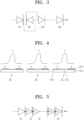
- FIG. 3 is a circuit diagram illustrating a sub-pixel arrangement of a display device using a semiconductor light-emitting device according to Present Example of the present disclosure.
- FIG. 4 is a schematic diagram illustrating a sub-pixel arrangement of a display device using a semiconductor light-emitting device according to Comparative Example.
- FIG. 5 is a circuit diagram illustrating a sub-pixel arrangement of a display device using a semiconductor light-emitting device according to Comparative Example.
- the first arrangement may be an arrangement in which the N-type electrode 235 is located on a left side and the P-type electrode 237 is located on a right side in FIG. 2 .
- the semiconductor layer 232 may be positioned on the substrate 231, and the first-type electrode, for example, the N-type electrode 235, and the second-type electrode, for example, the P-type electrode 237, in contact with such semiconductor layer 232 may be positioned.
- each of the light-emitting devices 230a, 230b, and 230c may have a light distribution a or b that is asymmetric with respect to the direction for connecting the first-type electrode 235 and the second-type electrode 237 to each other.
- the first light-emitting device 230a and the third light-emitting device 230c may have the light distribution a biased to the left. This may correspond to the first arrangement.
- the second light-emitting device 230b positioned between the first light-emitting device 230a and the third light-emitting device 230c may have the light distribution b biased to the right. This may correspond to the second arrangement.
- FIG. 4 shows a case in which light-emitting devices 23a, 23b, and 23c have the same arrangement b and the resulting light distribution b.
- the light-emitting device 23c has a semiconductor layer 23c-2 located on a substrate 23c-1, and includes a first-type electrode 23c-3 and a second-type electrode 23c-4 connected to the semiconductor layer 23c-2.
- FIG. 5 it may be seen that light-emitting devices D1, D2, D3, ..., Dn are connected to each other with the same arrangement.
- FIG. 2 shows a state in which the light distributions a and b of the light-emitting devices 230a, 230b, and 230c are biased toward the N-type electrode 235.
- the parasitic capacitance generated from a difference in electrical polarity between the light-emitting devices 230a, 230b, and 230c may be reduced.
- an electric field generated from the difference in the electric polarity between the light-emitting devices 230a, 230b, and 230c may be canceled.
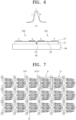
- FIG. 6 is a schematic diagram illustrating an effect of a sub-pixel arrangement of a display device using a semiconductor light-emitting device according to an embodiment of the present disclosure.
- the light-emitting devices 230b and 230c that are installed on the wiring substrate 100 and form the sub-pixels may be disposed.
- the wiring substrate 100 may include the wiring electrodes 123 and 124 including the first wiring electrode 123 and the second wiring electrode 124 arranged on the wiring substrate 100, and each of the light-emitting devices 230b and 230c may be installed to be electrically connected to the first wiring electrode 123 and the second wiring electrode 124 in each unit pixel area. That is, the sub-pixel arrangement in FIG. 6 may correspond to the case of the blue light-emitting device 230 in FIG. 1 .
- the light-emitting devices 230b and 230c may include a first light-emitting device 230b located in the first pixel area and installed in the first arrangement, and a second light-emitting device 230c located in the second pixel area adjacent to the first pixel area and installed in the second arrangement symmetrical to the first arrangement.
- Each of the first light-emitting device 230b and the second light-emitting device 230c may include the substrate 231, the semiconductor layer 232, the first-type electrode 235, and the second-type electrode 237.
- the first light-emitting device 230b and the second light-emitting device 230c may have different arrangements with respect to the direction for connecting the first-type electrode 235 and the second-type electrode 237 to each other.
- the light distribution a biased to one side by the first arrangement and the light distribution b biased to the other side by the second arrangement may be merged together to form a light distribution 'c' that is not biased and faces the center. That is, the asymmetrical light distributions may be canceled by the first arrangement of the first light-emitting device 230b and the second arrangement of the second light-emitting device 230c as described above.
- a positive voltage When a positive voltage is applied to a light emitting diode (LED) with a PN junction structure, charges and holes recombine with each other in an area where a P-area and an N-area meet each other to emit light.
- a portion where the greatest amount of light is emitted is not a center of the area where the P-area and the N-area meet each other, but is biased. Therefore, when a display is manufactured with such an LED, a color of the display may appear differently depending on a direction for viewing the display.
- FIG. 7 is a plan view illustrating an arrangement of wiring electrodes of a display device using a semiconductor light-emitting device according to Comparative Example.
- a common electrode 27 is disposed on a right side of each pixel area 24 for the entire arrangement of the three light-emitting devices.
- the two adjacent pixel areas 24 and 25 have the same arrangement with respect to the signal electrodes 24N and 24N+1 and the common electrode 27. Therefore, as described with reference to FIG. 4 , when the respective light-emitting devices installed in the same arrangement with respect to such signal electrodes 24N and 24N+1 and common electrode 27 constitute individual sub-pixels in a state of having the asymmetric light distribution b, and the individual sub-pixels constitute a display device, a problem in that, when viewing the display device from the outside, a color of the display appears differently depending on a viewing direction may occur.
- FIG. 8 is a plan view illustrating an arrangement of wiring electrodes of a display device using a semiconductor light-emitting device according to Present Example of the present disclosure.
- a center point 280 may be located between the two pixel areas 101 and 102, and such center point 280 may correspond to the second wiring electrode 124 described above. In addition, as mentioned above, the center point 280 may be connected to the second pads 140, 141, and 142.
- Such two pixel areas 101 and 102 may be located to be symmetrical with respect to each other around the center point 280. That is, the second wiring electrode 124 may be located between such two pixel areas 101 and 102.
- the light-emitting devices 230a, 230b, 230c, and 230d may have the asymmetric light distributions a and b with respect to the direction for connecting the first-type electrode 235 and the second-type electrode 237 to each other.
- the light-emitting devices 230a, 230b, 230c, and 230d may have the asymmetric light distributions a and b (see FIG. 2 ) with respect to the direction for connecting the first electrode pad 132 and the second electrode pad 142 to each other.
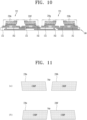
- FIG. 10 shows a state in which each of the light-emitting devices 230e, 230f, 230g, and 230h has a tilted crystal structure.
- the fifth light-emitting device 230e of one pixel and the sixth light-emitting device 230f of the other pixel may be tilted symmetrical to each other to have the same tilt angles in opposite directions.
- the fifth light-emitting device 230e and the sixth light-emitting device 230f may be tilted in a direction closer to each other.
- FIG. 11 schematically illustrates the state in which the pair of first light-emitting device 230a and second light-emitting device 230b are tilted in the direction away from each other in the first area 230 in FIG. 9 .
- the biased light distributions a and b caused by the crystal structure of the light-emitting devices may cancel each other. That is, the problem in that, when viewing the display device from the outside, the color of the display appears differently depending on the viewing direction may be solved.
- FIG. 12 is a schematic diagram illustrating a process of forming the sub-pixel arrangement according to FIG. 9 .
- the light-emitting devices 230a to 230d may be transferred to a transfer substrate 410 from a state of being positioned on a wafer 500, and then, transferred to the wiring substrate.
- the transfer substrate 410 may be, for example, a blue tape.
- the light-emitting devices 230a and 230c may be transferred to the transfer substrate 410 in an arrangement state as shown in 1 on an upper side (a reference point M of the wafer 500 is located on a left side).
- the light-emitting devices 230a and 230c transferred to the transfer substrate 410 may be transferred to the electrode pads in the odd-numbered rows of the wiring substrate #1, #3, and the like.
- the light-emitting devices 230b and 230d may be transferred to the transfer substrate 410.
- the light-emitting devices 230b and 230d transferred to the transfer substrate 410 may be transferred to the electrode pads in the even-numbered rows of the wiring substrate #2, #4, and the like.
- the light-emitting devices 230a to 230h having the arrangements as shown in FIGS. 9 to 11 may be transferred onto the wiring substrate.
- FIG. 13 is a side picture showing an individual light-emitting device of a display device using a semiconductor light-emitting device according to an embodiment of the present disclosure.
- FIG. 14 is a schematic diagram illustrating a tilt angle of an individual light-emitting device of a display device using a semiconductor light-emitting device according to an embodiment of the present disclosure.
- FIG. 13 is an enlarged picture showing a side surface of the blue light-emitting device 230.
- FIG. 13 may show a sapphire substrate occupying most of a thickness of the blue light-emitting device 230.
- a tilt angle a of the blue light-emitting device 230 may be approximately 10 degrees.
- a thickness t of the blue light-emitting device 230 may be 80 ⁇ m.
- the gallium nitride-based semiconductor layer positioned on the sapphire substrate may have the same or similar tilt angle.
- the sapphire substrate is removed after the light-emitting device is manufactured.
- the gallium nitride-based semiconductor layer, not the substrate may have the tilt angle as described above.
- FIG. 16 shows side pictures showing light-emitting devices of a display device using a semiconductor light-emitting device according to an embodiment of the present disclosure.
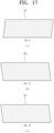
- FIG. 17 shows schematic diagrams illustrating tilt angles of light-emitting devices of a display device using a semiconductor light-emitting device according to an embodiment of the present disclosure.
- light-emitting devices that may be used in the display may have various tilt angles.
- a light-emitting device shown in (A) in FIG. 16 and (A) in FIG. 17 may have a tilt angle equal to or smaller than 5 degrees in one direction.
- a lateral cross-section of the light-emitting device has a parallelogram structure tilted to one side, so that, as described above, the light emitting device may have a light emitting pattern that is uneven and biased to one side with respect to the direction perpendicular to the surface.
- FIG. 18 is a graph illustrating an example of light distribution of a light-emitting device used in a display device using a semiconductor light-emitting device according to an embodiment of the present disclosure.
- FIG. 19 is a graph illustrating another example of light distribution of a light-emitting device used in a display device using a semiconductor light-emitting device according to an embodiment of the present disclosure.
- FIGS. 18 and 19 both show light intensity measured along a long axis (an x-axis) of the light-emitting device. That is, a center of the long axis corresponds to 0 degree, and the light intensity is expressed at left and right sides.
- FIG. 18 shows light distributions of respective red, green, and blue light-emitting devices. As shown, it may be seen that the light distributions are asymmetric at the left and right sides around the center.
- light distributions having a greater light intensity in a portion A on the right side based on 0 degrees is shown.
- light distributions having a greater light intensity in a portion B on the right side based on 0 degrees is shown.
- FIG. 20 shows light distribution uniformized as biased light distributions shown in FIG. 18 or 19 cancel each other. That is, referring to FIG. 20 , it may be seen that the light distribution as in FIG. 18 is uniformized based on the arrangement of the light-emitting devices described with reference to FIGS. 9 to 11 .
Landscapes
- Devices For Indicating Variable Information By Combining Individual Elements (AREA)
Abstract
Description
- The present disclosure is applicable to a display device-related technical field, and relates to, for example, a display device using a micro light emitting diode (LED).
- Recently, display devices with excellent characteristics such as thinness and flexibility are being developed in a field of display technology. Currently, commercially available major displays are represented by a liquid crystal display (LCD) and an organic light emitting diode (OLED).
- In one example, a light emitting diode (LED), as a well-known semiconductor light-emitting device that converts current into light, has been used as a light source for an image displayed in electronic devices including an information and communication device along with a GaP:N-based green LED, starting with commercialization of a red LED using a GaAsP compound semiconductor in 1962.
- Recently, such light emitting diode (LED) has been gradually miniaturized and manufactured as a micrometer-sized LED to be used for pixels or flat lighting of the display device.
- Sapphire, which is used as a substrate on which a gallium nitride-based semiconductor is grown, has a tilted crystal surface. For example, a R-plane has a crystal surface tilted along a m-axis. The ordinary sapphire may have the R-plane as a growth plane. Because the R-plane has a surface tilted with respect to a hexagonal prism crystal shape, the sapphire substrate and the gallium nitride-based semiconductor grown on the crystal surface of the sapphire substrate may have such a tilt angle.
- In addition, such a tilt angle may also be formed as a light-emitting device is formed as the gallium nitride-based semiconductor on the sapphire substrate and then is cut in a direction of the crystal surface of the sapphire substrate.
- Accordingly, when the light-emitting device is mounted on a wiring substrate in a general arrangement and emits light, an individual sub-pixel may be constructed in a state having an asymmetrical light distribution with respect to a direction for connecting two electrode pads with respect to one light-emitting device and the individual sub-pixels may constitute the display device.
- As such, when the display device is formed with the individual sub-pixels with the asymmetrical light distribution, a problem in that, when viewing the display device from the outside, a color of a display appears differently depending on a viewing direction may occur.
- In addition, an unintended parasitic capacitance may occur due to an electric field formed by a difference in polarity between a signal electrode/a common electrode of the light-emitting device.
- Accordingly, even when the electric field is dissipated, discharge of the parasitic capacitance may not be normally performed, and thus a situation in which an adjacent light-emitting device is unintentionally turned on may occur.
- The corresponding effect may be accumulated by the total number of light-emitting devices used in the display device, and finally, a ghost phenomenon may appear in a unit of a display product.
- Therefore, there is a demand for a method capable of solving such problem.
- The present disclosure is to provide a display device using a semiconductor light-emitting device that may cancel the biased light distributions of the light-emitting devices caused by the crystallinity of the light-emitting devices.
- In addition, the present disclosure is to provide a display device using a semiconductor light-emitting device that may solve a problem in that, when viewing the display device from the outside, a color of a display appears differently depending on a viewing direction.
- In addition, the present disclosure is to provide a display device using a semiconductor light-emitting device that may reduce a parasitic capacitance caused by a difference in electrical polarity between the light-emitting devices.
- In addition, the present disclosure is to provide a display device using a semiconductor light-emitting device that may cancel an electric field generated by a difference in electrical polarity between the light-emitting devices.
- In addition, according to an embodiment of the present disclosure, the present disclosure is to provide a display device using a semiconductor light-emitting device that may visually reinforce an area with weak color when viewing the display from one side to correct a color difference of the display perceived on left and right sides.
- A display device using a light-emitting device according to the present disclosure includes a wiring substrate having multiple unit pixel areas defined therein, a wiring electrode including first wiring electrodes and a second wiring electrode arranged on the wiring substrate, and each light-emitting device installed in each unit pixel area so as to be electrically connected to each first wiring electrode and the second wiring electrode to constitute each sub-pixel, and the light-emitting devices include a first light-emitting device located in a first pixel area and installed in a first arrangement, and a second light-emitting device located in a second pixel area adjacent to the first pixel area and installed in a second arrangement symmetrical to the first arrangement.
- According to an embodiment, a parasitic capacitance generated by a difference in electrical polarity between the first light-emitting device and the second light-emitting device may be reduced by the first arrangement and the second arrangement.
- According to an embodiment, positions of electrodes of the first light-emitting device and the second light-emitting device may be symmetrical to each other in the first arrangement and the second arrangement.
- According to an embodiment, the first wiring electrode corresponding to the first pixel area and an adjacent first wiring electrode corresponding to the second pixel area may be symmetrically positioned with respect to each other around a center point between the first pixel area and the second pixel area.
- According to an embodiment, the center point between the first pixel area and the second pixel area may correspond to the second wiring electrode.
- According to an embodiment, the first pixel area and the second pixel area may form a pair between the first wiring electrode and a first wiring electrode adjacent thereto.
- According to an embodiment, an electric field generated by a difference in electric polarity between the first light-emitting device and the second light-emitting device may be canceled by the first arrangement and the second arrangement.
- According to an embodiment, a side surface of each of the first light-emitting device and the second light-emitting device may be tilted to have a tilt angle.
- According to an embodiment, the first light-emitting device and the second light-emitting device may be tilted symmetrical to each other to have the same tilt angles in opposite directions by the first arrangement and the second arrangement.
- According to an embodiment, each light-emitting device may include a first-type electrode and a second-type electrode, and have an asymmetric light distribution with respect to a direction for connecting the first-type electrode and the second-type electrode to each other.
- According to an embodiment, the asymmetric light distributions may be canceled with each other by the first arrangement and the second arrangement.
- According to an embodiment, the first light-emitting device and the second light-emitting device may emit light of the same color.
- A display device using a light-emitting device according to the present disclosure includes a wiring substrate having multiple unit pixel areas defined therein, a wiring electrode including first wiring electrodes and a second wiring electrode arranged on the wiring substrate, and each light-emitting device installed in each unit pixel area so as to be electrically connected to each first wiring electrode and the second wiring electrode to constitute each sub-pixel, and the light-emitting devices include a first light-emitting device located in a first sub-pixel area and installed in a first arrangement, and a second light-emitting device located in a second sub-pixel area adjacent to the first sub-pixel area and installed in a second arrangement symmetrical to the first arrangement with respect to the first wiring electrode.
- According to one embodiment of the present disclosure, the following effects are obtained.
- First, according to one embodiment of the present disclosure, the biased light distributions of the light-emitting devices resulting from the crystallinity of the light-emitting devices may be cancelled with each other. That is, the asymmetrical light distributions of the light-emitting devices may be canceled.
- Accordingly, the problem in that, when viewing the display device from the outside, the color of the display appears differently depending on the viewing direction may be solved.
- In addition, according to one embodiment of the present disclosure, the parasitic capacitance generated by the difference in the electrical polarity of the light-emitting devices may be reduced.
- In addition, the ghost phenomenon that may occur due to such parasitic capacitance may be reduced.
- In addition, according to one embodiment of the present disclosure, the electric field generated by the difference in the electrical polarity between the light-emitting devices may be canceled.
- In addition, according to one embodiment of the present disclosure, the area with the weak color may be visually reinforced when viewing the display from one direction to correct the color difference between the left and right sides of the display. Therefore, the effect of enhancing the color viewing angle in the final product stage of the display device may be obtained.
- Furthermore, according to another embodiment of the present disclosure, there are additional technical effects not mentioned here. A person skilled in the art may understand this via the entire meaning of the present document and drawings.
-
-
FIG. 1 is a schematic diagram of a display device using a semiconductor light-emitting device according to an embodiment of the present disclosure. -
FIG. 2 is a schematic diagram illustrating a sub-pixel arrangement of a display device using a semiconductor light-emitting device according to Present Example of the present disclosure. -
FIG. 3 is a circuit diagram illustrating a sub-pixel arrangement of a display device using a semiconductor light-emitting device according to Present Example of the present disclosure. -
FIG. 4 is a schematic diagram illustrating a sub-pixel arrangement of a display device using a semiconductor light-emitting device according to Comparative Example. -
FIG. 5 is a circuit diagram illustrating a sub-pixel arrangement of a display device using a semiconductor light-emitting device according to Comparative Example. -
FIG. 6 is a schematic diagram illustrating an effect of a sub-pixel arrangement of a display device using a semiconductor light-emitting device according to an embodiment of the present disclosure. -
FIG. 7 is a plan view illustrating an arrangement of wiring electrodes of a display device using a semiconductor light-emitting device according to Comparative Example. -
FIG. 8 is a plan view illustrating an arrangement of wiring electrodes of a display device using a semiconductor light-emitting device according to Present Example of the present disclosure. -
FIG. 9 is a schematic diagram illustrating a specific example of a sub-pixel arrangement of a display device using a semiconductor light-emitting device according to an embodiment of the present disclosure. -
FIG. 10 is a schematic diagram showing another specific example of a sub-pixel arrangement of a display device using a semiconductor light-emitting device according to an embodiment of the present disclosure. -
FIG. 11 is a diagram schematically illustrating sub-pixel arrangements inFIGS. 9 and10 . -
FIG. 12 is a schematic diagram illustrating a process of forming the sub-pixel arrangement according toFIG. 9 . -
FIG. 13 is a side picture showing an individual light-emitting device of a display device using a semiconductor light-emitting device according to an embodiment of the present disclosure. -
FIG. 14 is a schematic diagram illustrating a tilt angle of an individual light-emitting device of a display device using a semiconductor light-emitting device according to an embodiment of the present disclosure. -
FIG. 15 schematically illustrates a crystal surface and a crystal direction of sapphire. -
FIG. 16 shows side pictures showing light-emitting devices of a display device using a semiconductor light-emitting device according to an embodiment of the present disclosure. -
FIG. 17 shows schematic diagrams illustrating tilt angles of light-emitting devices of a display device using a semiconductor light-emitting device according to an embodiment of the present disclosure. -
FIG. 18 is a graph illustrating an example of light distribution of a light-emitting device used in a display device using a semiconductor light-emitting device according to an embodiment of the present disclosure. -
FIG. 19 is a graph illustrating another example of light distribution of a light-emitting device used in a display device using a semiconductor light-emitting device according to an embodiment of the present disclosure. -
FIG. 20 shows light distribution uniformized as biased light distributions shown inFIG. 18 or19 cancel each other. - Reference will now be made in detail to embodiments of the present disclosure, examples of which are illustrated in the accompanying drawings. Wherever possible, the same reference numbers will be used throughout the drawings to refer to the same or like parts, and redundant description thereof will be omitted. As used herein, the suffixes "module" and "unit" are added or used interchangeably to facilitate preparation of this specification and are not intended to suggest distinct meanings or functions. In describing embodiments disclosed in this specification, relevant well-known technologies may not be described in detail in order not to obscure the subject matter of the embodiments disclosed in this specification. In addition, it should be noted that the accompanying drawings are only for easy understanding of the embodiments disclosed in the present specification, and should not be construed as limiting the technical spirit disclosed in the present specification.
- Furthermore, although the drawings are separately described for simplicity, embodiments implemented by combining at least two or more drawings are also within the scope of the present disclosure.
- In addition, when an element such as a layer, region or module is described as being "on" another element, it is to be understood that the element may be directly on the other element or there may be an intermediate element between them.
- A semiconductor light-emitting device mentioned herein is a concept including an LED, a micro LED, and the like, and is able to be used interchangeably with those.
-
FIG. 1 is a schematic diagram of a display device using a semiconductor light-emitting device according to an embodiment of the present disclosure. - Referring to
FIG. 1 , in adisplay device 10, an individualunit pixel area 101 may be partitioned on awiring substrate 100, and multiple light-emitting devices 200: 210, 220, and 230 may be installed within suchunit pixel area 101. - In this regard, the individual light-emitting
devices unit pixel area 101 may substantially correspond to sub-pixels, respectively. For example, three sub-pixels may be gathered to constitute one pixel. InFIG. 1 , the three light-emittingdevices - Each of the light-emitting
devices electrode pads electrode pads FIG. 1 may be connected to first wiring electrodes (signal electrodes or data electrodes) 121, 122, and 123, respectively. - In addition, the
electrode pads FIG. 1 , the signal electrodes 121, 122, and 123 and the common electrode 124 are omitted due to an arrangement of electrodes and pads. - In one example, in some cases, the
first electrode pads second electrode pads - Hereinafter, reference numerals of the electrode pads and the wiring electrodes are used interchangeably for description. That is, the electrode pads and the wire electrodes may be described using the same reference numerals.
- As such, unit sub-pixels may be defined at points where the first wiring electrodes 121, 122, and 123 and the second wiring electrode 124 intersect each other.
- In one example, when the first wiring electrodes 121, 122, and 123 are the signal electrodes (or the data electrodes), such first wiring electrodes 121, 122, and 123 or the
first electrode pads TFT layer 120 on which a thin film transistor (TFT) is disposed. Accordingly, each of the light-emittingdevices such TFT layer 120. - In
FIG. 1 , theTFT layer 120 is briefly shown as a single layer, but theTFT layer 120 may include multiple TFT areas capable of performing the switching operation. For example, each TFT area may include a gate electrode, a source electrode, a drain electrode, an insulating layer disposed therebetween, a via electrode that may be connected to the first wiring electrodes 121, 122, and 123 or thefirst electrode pads devices - The multiple light-emitting
devices 200; 210, 220, and 230 may be installed to be electrically connected onto the wiring electrodes 121, 122, 123, and 124 to form individual sub-pixels. - As mentioned above, such light-emitting
devices 200 may include the red light-emittingdevice 210, the green light-emittingdevice 220, and the blue light-emittingdevice 230, and such three light-emittingdevices wiring substrate 100. Such light-emittingdevices devices - Such semiconductor light-emitting device (LED) 200 may have a size of a micrometer (µm) unit. The micrometer (µm) size may mean that a width of at least one surface of the light-emitting
device 200 has a size of several to hundreds of micrometers (µm). - The
TFT layer 120 may be positioned on asubstrate 110, and an insulatinglayer 150 may be coated on theTFT layer 120. Such insulatinglayer 150 may be coated on a connection portion between the wiring electrodes 121, 122, 123, and 124, theelectrode pads devices - For example, the individual light-emitting
devices partition wall 160. In addition, acover layer 170 may be positioned on the light-emittingdevices partition wall 160. - As described above, the light-emitting
devices wiring substrate 100. For example, eachpixel area 101 may be repeatedly disposed on thewiring substrate 100. - In this regard, the
pixel areas 101 may be repeatedly positioned along one line of the data electrodes (the first wiring electrodes) 121, 122, and 123 or line of the scan electrode (the second wiring electrode) 124 in a longitudinal direction. For example, inFIG. 1 , the red light-emittingdevice 210, the green light-emittingdevice 220, and the blue light-emittingdevice 230 may be repeatedly positioned along a left and right direction. For example, a red light-emitting device of an adjacent pixel area may be positioned on a right side of the blue light-emittingdevice 230. - In one example, another data electrode (first wiring electrode) line or scan electrode (second wiring electrode) line adjacent to one data electrode (first wiring electrode) line or scan electrode (second wiring electrode) line in a parallel manner may be located (see
FIG. 8 ). In this regard, a pixel area 102 (seeFIG. 8 ) having the same arrangement of the light-emittingdevices pixel area 101 may be located on the adjacent data electrode (first wiring electrode) line or scan electrode (second wiring electrode) line. - In this case, light-emitting devices having the same color may be located adjacent to each other in adjacent pixel areas. For example, the red light-emitting
device 210, the green light-emittingdevice 220, and the blue light-emittingdevice 230 may be repeatedly positioned along the data electrode (first wiring electrode) line or the scan electrode (second wiring electrode) line, but light-emitting devices having the same color may be repeatedly positioned in a direction perpendicular to such data electrode (first wiring electrode) line or the scan electrode (second wiring electrode) line. - In this regard, according to one embodiment of the present disclosure, two adjacent light-emitting devices may have different arrangements. For example, referring to
FIG. 1 , the red light-emittingdevice 210 and the green light-emittingdevice 220 adjacent to the red light-emittingdevice 210 may have different arrangements. - For example, in the red light-emitting
device 210, a first-type electrode, for example, an N-type electrode, may be positioned on thefirst wiring electrode 130, and in the green light-emittingdevice 220, a second-type electrode, for example, a P-type electrode, may be positioned on thefirst wiring electrode 131. Such different arrangements may also be made on the green light-emittingdevice 220 and the blue light-emittingdevice 230. - That is, the red light-emitting
device 210 and the green light-emittingdevice 220 adjacent to such red light-emittingdevice 210 may have symmetrical arrangements with respect to electrode positions of the respective light-emittingdevices - In one example, a light-emitting device (e.g., the red light-emitting device 210) located in one
pixel area 101 and a light-emitting device (e.g., the red light-emitting device 210) located in theadjacent pixel area 102 may have symmetrical arrangements with respect to the electrode positions as described above. - In other words, on the
wiring substrate 100, a first light-emittingdevice 210 located in thefirst pixel area 101 and installed in a first arrangement, and a second light-emittingdevice 210 located in thesecond pixel area 102 adjacent to suchfirst pixel area 101 and installed in a second arrangement symmetric with respect to the first arrangement may be positioned. - With the first and second arrangements of the light-emitting
devices 210 as described above, a parasitic capacitance generated from a difference in electrical polarity between the first light-emitting device and the second light-emitting device may be reduced. - In addition, with the first arrangement and the second arrangement of the light-emitting
devices 210 as described above, an electric field generated from the difference in the electric polarity between the first light-emitting device and the second light-emitting device may be canceled. - The light-emitting
devices 210 having such different arrangements and effects thereof will be described later in detail. -
FIG. 2 is a schematic diagram illustrating a sub-pixel arrangement of a display device using a semiconductor light-emitting device according to Present Example of the present disclosure. In addition,FIG. 3 is a circuit diagram illustrating a sub-pixel arrangement of a display device using a semiconductor light-emitting device according to Present Example of the present disclosure. -
FIG. 4 is a schematic diagram illustrating a sub-pixel arrangement of a display device using a semiconductor light-emitting device according to Comparative Example.FIG. 5 is a circuit diagram illustrating a sub-pixel arrangement of a display device using a semiconductor light-emitting device according to Comparative Example. - Referring to
FIG. 2 , a state in which a first light-emittingdevice 230a and a second light-emittingdevice 230b adjacent to each other are positioned in different arrangements, the first arrangement and second arrangement, is shown. In addition, the second light-emittingdevice 230b and a third light-emittingdevice 230c may also be positioned in different arrangements. Referring toFIG. 3 , it may be seen that light-emitting devices D1*, D2*, D3*, ..., Dn* may be connected to each other in arrangements that alternate and are opposite to each other. - For example, the first light-emitting
device 230a and the third light-emittingdevice 230c may be positioned in the first arrangement, and the second light-emittingdevice 230b positioned between the first light-emittingdevice 230a and the third light-emittingdevice 230c may be positioned in the second arrangement. - In this regard, the first light-emitting
device 230a, the second light-emittingdevice 230b, and the third light-emittingdevice 230c may all be light-emitting devices that emit light of the same color. For example, the first light-emittingdevice 230a, the second light-emittingdevice 230b, and the third light-emittingdevice 230c may all be the blue light-emitting devices. - In this regard, the first arrangement may be an arrangement in which the N-
type electrode 235 is located on a left side and the P-type electrode 237 is located on a right side inFIG. 2 . In each of the light-emittingdevices semiconductor layer 232 may be positioned on thesubstrate 231, and the first-type electrode, for example, the N-type electrode 235, and the second-type electrode, for example, the P-type electrode 237, in contact withsuch semiconductor layer 232 may be positioned. - That is, each of the light-emitting
devices substrate 231, thesemiconductor layer 232, the first-type electrode 235, and the second-type electrode 237. In this regard, each of the light-emittingdevices type electrode 235 and the second-type electrode 237 to each other. - Referring to
FIG. 2 , each of the light-emittingdevices type electrode 235 and the second-type electrode 237 to each other. For example, the first light-emittingdevice 230a and the third light-emittingdevice 230c may have the light distribution a biased to the left. This may correspond to the first arrangement. In addition, the second light-emittingdevice 230b positioned between the first light-emittingdevice 230a and the third light-emittingdevice 230c may have the light distribution b biased to the right. This may correspond to the second arrangement. - This may be resulted from material characteristics of at least one of the
substrate 231 and thesemiconductor layer 232. For example, such phenomenon may occur because a crystal structure of at least one of thesubstrate 231 and thesemiconductor layer 232 has a tilted shape. This will be described later in detail. - As Comparative Example,
FIG. 4 shows a case in which light-emittingdevices device 23c has asemiconductor layer 23c-2 located on asubstrate 23c-1, and includes a first-type electrode 23c-3 and a second-type electrode 23c-4 connected to thesemiconductor layer 23c-2. Referring toFIG. 5 , it may be seen that light-emitting devices D1, D2, D3, ..., Dn are connected to each other with the same arrangement. - As shown in
FIG. 4 , when each of the light-emittingdevices type electrode 23c-3 and the second-type electrode 23c-4 and the individual sub-pixels constitute the display device, a problem in that, when viewing the display device from the outside, a color of a display appears differently depending on a viewing direction may occur. - In the polar arrangement of the light-emitting
devices type electrode 23c-3 and the second-type electrode 23c-4 are sequentially repeated, so that the unintended parasitic capacitance may occur due to an electric field formed by a difference in polarity between the first-type electrode 23c-3 and the second-type electrode 23c-4 (or between a signal electrode/a common electrode connected thereto) of each of the light-emittingdevices - Accordingly, even when the electric field is dissipated, discharge of the parasitic capacitance is not normally performed, so that a situation in which an adjacent light-emitting device is unintentionally turned on may occur. For example, when the D3 is in an ON state, the D1 and the D2, which should be in an OFF state, may unintentionally remain in the ON state. The corresponding effect may be accumulated by the total number of light-emitting
devices - However, as in Present Example of the present disclosure, when the adjacent light-emitting
devices type electrode 235 and the second-type electrode 237 to each other, such problem may be solved. - As an embodiment,
FIG. 2 shows a state in which the light distributions a and b of the light-emittingdevices type electrode 235. However, this is merely an example, not all of the light distributions of the light-emittingdevices type electrode 235. That is, in one example, the light distributions of the light-emittingdevices type electrode 237. - Therefore, with the different arrangements with respect to the direction for connecting the first-
type electrodes 235 to the second-type electrodes 237 of the adjacent light-emittingdevices - With the first arrangement and the second arrangement of the light-emitting
devices devices - In addition, with such first arrangement and second arrangement of the light-emitting
devices devices -
FIG. 6 is a schematic diagram illustrating an effect of a sub-pixel arrangement of a display device using a semiconductor light-emitting device according to an embodiment of the present disclosure. - Referring to
FIG. 6 , the light-emittingdevices wiring substrate 100 and form the sub-pixels may be disposed. - In this regard, referring to (B) in
FIG. 6 on a lower side, as described with reference toFIG. 1 above, thewiring substrate 100 may include the wiring electrodes 123 and 124 including the first wiring electrode 123 and the second wiring electrode 124 arranged on thewiring substrate 100, and each of the light-emittingdevices FIG. 6 may correspond to the case of the blue light-emittingdevice 230 inFIG. 1 . - In this regard, referring to (A) and (B) in
FIG. 6 together, the light-emittingdevices device 230b located in the first pixel area and installed in the first arrangement, and a second light-emittingdevice 230c located in the second pixel area adjacent to the first pixel area and installed in the second arrangement symmetrical to the first arrangement. - Each of the first light-emitting
device 230b and the second light-emittingdevice 230c may include thesubstrate 231, thesemiconductor layer 232, the first-type electrode 235, and the second-type electrode 237. In this regard, the first light-emittingdevice 230b and the second light-emittingdevice 230c may have different arrangements with respect to the direction for connecting the first-type electrode 235 and the second-type electrode 237 to each other. - Accordingly, the light distribution a biased to one side by the first arrangement and the light distribution b biased to the other side by the second arrangement may be merged together to form a light distribution 'c' that is not biased and faces the center. That is, the asymmetrical light distributions may be canceled by the first arrangement of the first light-emitting
device 230b and the second arrangement of the second light-emittingdevice 230c as described above. - In this regard, as described above, the first light-emitting
device 230b and the second light-emittingdevice 230c may be light-emitting devices that emit light of the same color located in the adjacent pixel areas, for example, the blue light-emitting devices. - When a positive voltage is applied to a light emitting diode (LED) with a PN junction structure, charges and holes recombine with each other in an area where a P-area and an N-area meet each other to emit light. In this regard, a portion where the greatest amount of light is emitted is not a center of the area where the P-area and the N-area meet each other, but is biased. Therefore, when a display is manufactured with such an LED, a color of the display may appear differently depending on a direction for viewing the display.
- However, as described above, when the first arrangement of the first light-emitting
device 230b and the second arrangement of the second light-emittingdevice 230c are symmetrical with each other, a color difference of the display perceived on left and right sides when viewing the display from one side may be compensated for by visually reinforcing an area with weak color. Therefore, an effect of enhancing a color viewing angle in a final product stage of the display device may be obtained. - In addition, an electric field formed by a difference in polarity between the light-emitting
devices device 230b and the second light-emittingdevice 230c, so that a parasitic capacitance may be prevented from being generated. In addition, the ghost phenomenon that may occur due to such parasitic capacitance may be improved. -
FIG. 7 is a plan view illustrating an arrangement of wiring electrodes of a display device using a semiconductor light-emitting device according to Comparative Example. -
FIG. 7 shows an arrangement of wiring electrodes corresponding to the arrangement of light-emittingdevices FIG. 4 above. Referring toFIG. 7 , somepixel areas - In addition, it may be seen that a common electrode 27 is disposed on a right side of each
pixel area 24 for the entire arrangement of the three light-emitting devices. - Referring to
FIG. 7 , the twoadjacent pixel areas FIG. 4 , when the respective light-emitting devices installed in the same arrangement with respect to such signal electrodes 24N and 24N+1 and common electrode 27 constitute individual sub-pixels in a state of having the asymmetric light distribution b, and the individual sub-pixels constitute a display device, a problem in that, when viewing the display device from the outside, a color of the display appears differently depending on a viewing direction may occur. -
FIG. 8 is a plan view illustrating an arrangement of wiring electrodes of a display device using a semiconductor light-emitting device according to Present Example of the present disclosure. -
FIG. 8 shows an arrangement of wiring electrodes corresponding to the arrangement of the light-emittingdevices FIG. 2 above. Referring toFIG. 8 , somepixel areas - A
center point 280 may be located between the twopixel areas such center point 280 may correspond to the second wiring electrode 124 described above. In addition, as mentioned above, thecenter point 280 may be connected to thesecond pads - Such two
pixel areas center point 280. That is, the second wiring electrode 124 may be located between such twopixel areas - As described above, the three light-emitting
devices pixel area 101 to constitute the respective sub-pixels. In this regard, because the twopixel areas center point 280, the three light-emittingdevices pixel area 101 may be located so as to be symmetrical with respect to the three light-emittingdevices pixel area 102, respectively. - In this regard, the respective light-emitting
devices holes 260, and signals may be supplied from such signal electrodes. In addition, thecenter point 280 connected to the second wiring electrode 124 may also correspond to the via hole. - That is, when taking a light-emitting device rendering one color, for example, the blue light-emitting
device 230, as an example, the first light-emittingdevice 230b (seeFIG. 6 ) located in thefirst pixel area 101 and installed in the first arrangement, and the second light-emittingdevice 230c (seeFIG. 6 ) located in thesecond pixel area 102 adjacent to thefirst pixel area 101 and installed in the second arrangement symmetrical to the first arrangement may be located. - In addition, the
pixel areas FIG. 8 , the first wiring electrodes 270N, 270N+1, and the like may be located on both sides of the pair ofpixel areas - As such, because the three light-emitting
devices pixel area 101 and the three light-emittingdevices pixel area 102 are positioned symmetrically with respect to each other around the second wiring electrode 124, one light-emitting device and a counterpart thereof are disposed such that electrodes of the same polarity face each other, thereby using a via hole in common. Therefore, the number of via holes for supplying power to the light-emittingdevices FIG. 7 , and the number of scan electrodes (second wiring electrodes) 124 may also be reduced compared to that in the case inFIG. 7 . - The via hole is caused by an inductance component, so that there is a possibility that the via hole may be mixed with a signal noise component. Therefore, it is advantageous when the number of via holes is as small as possible in a circuit substrate. As such, according to the embodiment of the present disclosure, a signal may be further stabilized by reducing the number of via holes. In addition, a difficulty of manufacturing the circuit substrate may be reduced, and accordingly, a manufacturing time and a manufacturing cost of the circuit substrate may be reduced.
- In addition, as described above, the electric field formed by the difference in the polarity between the light-emitting
devices device 230b and the second light-emittingdevice 230c, so that the occurrence of the parasitic capacitance may be prevented. - In general, the capacitance exhibits a characteristic that is inversely proportional to a distance. With the circuit pattern shown in
FIG. 8 , because a distance between the first wiring electrodes 270N, 270N+1, and the like is approximately doubled with respect to thepixel areas -
FIG. 9 is a schematic diagram illustrating a specific example of a sub-pixel arrangement of a display device using a semiconductor light-emitting device according to an embodiment of the present disclosure. - Referring to
FIG. 9 , a state in which light-emittingdevices wiring substrate 100 is shown. This may correspond to a state in which the arrangement of the light-emitting devices shown inFIG. 6 continues in a parallel manner. - As mentioned above, the light-emitting
devices type electrode 235 and the second-type electrode 237 to each other. In addition, the light-emittingdevices FIG. 2 ) with respect to the direction for connecting thefirst electrode pad 132 and thesecond electrode pad 142 to each other. - For example, the first light-emitting
device 230a and the third light-emittingdevice 230c may have the light distribution a biased to the left. This may correspond to the first arrangement. In addition, the second light-emittingdevice 230b positioned between the first light-emittingdevice 230a and the third light-emittingdevice 230c and the fourth light-emittingdevice 230d positioned on a right side of the third light-emittingdevice 230c may have the light distribution b biased to the right. This may correspond to the second arrangement. - This may be resulted from the material characteristics of at least one of the
substrate 231 and thesemiconductor layer 232. For example, such phenomenon may occur because the crystal structure of at least one of thesubstrate 231 and thesemiconductor layer 232 has the tilted shape. This will be described later in detail. -
FIG. 9 shows a state in which each of the light-emittingdevices device 230a of one pixel and the second light-emittingdevice 230b of the other pixel may be tilted symmetrical to each other to have the same tilt angles in opposite directions. For example, the first light-emittingdevice 230a and the second light-emittingdevice 230b may be tilted in a direction away from each other. In addition, in asecond area 231 adjacent to thefirst area 230, the third light-emittingdevice 230c and the fourth light-emittingdevice 230d of the other pixel may be tilted symmetrical to each other to have the same tilt angles in opposite directions. -
FIG. 10 is a schematic diagram showing another specific example of a sub-pixel arrangement of a display device using a semiconductor light-emitting device according to an embodiment of the present disclosure. - Referring to
FIG. 10 , a state in which light-emittingdevices wiring substrate 100 is shown. This may correspond to the state in which the arrangement of the light-emitting devices shown inFIG. 6 continues in the parallel manner. - As mentioned above, the light-emitting
devices type electrode 235 and the second-type electrode 237 to each other. In addition, the light-emittingdevices FIG. 2 ) with respect to the direction for connecting thefirst electrode pad 132 and thesecond electrode pad 142 to each other. -
FIG. 10 shows a state in which each of the light-emittingdevices device 230e of one pixel and the sixth light-emittingdevice 230f of the other pixel may be tilted symmetrical to each other to have the same tilt angles in opposite directions. For example, the fifth light-emittingdevice 230e and the sixth light-emittingdevice 230f may be tilted in a direction closer to each other. In addition, in afourth area 233 adjacent to thethird area 232, the seventh light-emittingdevice 230g and the eighth light-emittingdevice 230h of the other pixel may have be tilted symmetrical to each other to have the same tilt angles in opposite directions. -
FIG. 11 is a diagram schematically illustrating sub-pixel arrangements inFIGS. 9 and10 . - (a) in
FIG. 11 schematically illustrates the state in which the pair of first light-emittingdevice 230a and second light-emittingdevice 230b are tilted in the direction away from each other in thefirst area 230 inFIG. 9 . - In addition, (b) in
FIG. 11 schematically illustrates the state in which the pair of the fifth light-emittingdevice 230e and the sixth light-emittingdevice 230f are tilted in the direction closer to each other in thethird area 232 inFIG. 10 . - As described above, when the light-emitting devices in the pixels adjacent to each other are paired with each other and positioned symmetrical with respect to each other, the biased light distributions a and b caused by the crystal structure of the light-emitting devices may cancel each other. That is, the problem in that, when viewing the display device from the outside, the color of the display appears differently depending on the viewing direction may be solved.
-
FIG. 12 is a schematic diagram illustrating a process of forming the sub-pixel arrangement according toFIG. 9 . - An example of a method for transferring the light-emitting devices to have the different arrangements will be briefly described with reference to
FIG. 12 . - For example, the light-emitting
devices wiring substrate # 1, #3, and the like, and then the light-emittingdevices wiring substrate # 2, #4, and the like after rotating the positions of the light-emitting devices by 180 degrees. - The light-emitting
devices 230a to 230d may be transferred to atransfer substrate 410 from a state of being positioned on awafer 500, and then, transferred to the wiring substrate. In this regard, thetransfer substrate 410 may be, for example, a blue tape. - First, the light-emitting
devices transfer substrate 410 in an arrangement state as shown in ① on an upper side (a reference point M of thewafer 500 is located on a left side). - Subsequently, the light-emitting
devices transfer substrate 410 may be transferred to the electrode pads in the odd-numbered rows of thewiring substrate # 1, #3, and the like. - Thereafter, in a state in which the
wafer 500 is rotated by 180 degrees as shown in ② on a lower side (the reference point M of thewafer 500 is located on a right side), the light-emittingdevices transfer substrate 410. - Subsequently, the light-emitting
devices transfer substrate 410 may be transferred to the electrode pads in the even-numbered rows of thewiring substrate # 2, #4, and the like. - With such process, the light-emitting
devices 230a to 230h having the arrangements as shown inFIGS. 9 to 11 may be transferred onto the wiring substrate. -
FIG. 13 is a side picture showing an individual light-emitting device of a display device using a semiconductor light-emitting device according to an embodiment of the present disclosure.FIG. 14 is a schematic diagram illustrating a tilt angle of an individual light-emitting device of a display device using a semiconductor light-emitting device according to an embodiment of the present disclosure. -
FIG. 13 is an enlarged picture showing a side surface of the blue light-emittingdevice 230.FIG. 13 may show a sapphire substrate occupying most of a thickness of the blue light-emittingdevice 230. As shown inFIG. 14 , a tilt angle a of the blue light-emittingdevice 230 may be approximately 10 degrees. In addition, as an example, a thickness t of the blue light-emittingdevice 230 may be 80 µm. - However, the gallium nitride-based semiconductor layer positioned on the sapphire substrate may have the same or similar tilt angle. In some cases, the sapphire substrate is removed after the light-emitting device is manufactured. In this case, in the light-emitting device, the gallium nitride-based semiconductor layer, not the substrate, may have the tilt angle as described above.
-
FIG. 15 schematically illustrates a crystal surface and a crystal direction of sapphire. The sapphire may be used as a growth substrate for a light-emitting device made of a gallium nitride-based semiconductor. - As shown, the sapphire has a tilted crystal surface. As an example, an R-plane has a crystal surface tilted along an m-axis. Ordinary sapphire may have the R-plane as a growth plane thereof. Referring to
FIG. 15 , because the R-plane has a tilted plane with respect to a hexagonal prism crystal shape, the sapphire substrate and the gallium nitride-based semiconductor grown on the crystal surface of the sapphire substrate may have such a tilt angle. - In addition, such a tilt angle may also be formed as the light-emitting device is formed as the gallium nitride-based semiconductor on the sapphire substrate and then is cut in the direction of the crystal surface of the sapphire substrate.
-
FIG. 16 shows side pictures showing light-emitting devices of a display device using a semiconductor light-emitting device according to an embodiment of the present disclosure. In addition,FIG. 17 shows schematic diagrams illustrating tilt angles of light-emitting devices of a display device using a semiconductor light-emitting device according to an embodiment of the present disclosure. - Referring to
FIGS. 16 and17 , light-emitting devices that may be used in the display may have various tilt angles. As an example, a light-emitting device shown in(A) in FIG. 16 and(A) in FIG. 17 may have a tilt angle equal to or smaller than 5 degrees in one direction. - In addition, a light-emitting device shown in
(B) in FIG. 16 and(B) in FIG. 17 may have a tilt angle equal to or smaller than 12 degrees in a direction opposite to that of the tilt angle of the light-emitting device shown in(A) in FIG. 16 and(A) in FIG. 17 . - Further, a light-emitting device shown in
(C) in FIG. 16 and(C) in FIG. 17 may have a tilt angle equal to or smaller than 10 degrees in the same direction as that of the tilt angle of the light-emitting device shown in(B) in FIG. 16 and(B) in FIG. 17 . - As such, a lateral cross-section of the light-emitting device has a parallelogram structure tilted to one side, so that, as described above, the light emitting device may have a light emitting pattern that is uneven and biased to one side with respect to the direction perpendicular to the surface.
-
FIG. 18 is a graph illustrating an example of light distribution of a light-emitting device used in a display device using a semiconductor light-emitting device according to an embodiment of the present disclosure.FIG. 19 is a graph illustrating another example of light distribution of a light-emitting device used in a display device using a semiconductor light-emitting device according to an embodiment of the present disclosure. -
FIGS. 18 and19 both show light intensity measured along a long axis (an x-axis) of the light-emitting device. That is, a center of the long axis corresponds to 0 degree, and the light intensity is expressed at left and right sides. -
FIG. 18 shows light distributions of respective red, green, and blue light-emitting devices. As shown, it may be seen that the light distributions are asymmetric at the left and right sides around the center. - Referring to
FIG. 18 , light distributions having a greater light intensity in a portion A on the right side based on 0 degrees is shown. Similarly, referring toFIG. 19 , light distributions having a greater light intensity in a portion B on the right side based on 0 degrees is shown. -
FIG. 20 shows light distribution uniformized as biased light distributions shown inFIG. 18 or19 cancel each other. That is, referring toFIG. 20 , it may be seen that the light distribution as inFIG. 18 is uniformized based on the arrangement of the light-emitting devices described with reference toFIGS. 9 to 11 . - As such, when the light-emitting devices in the pixels adjacent to each other are paired with each other and positioned symmetrical with respect to each other, the biased light distributions a and b caused by the crystal structure of the light-emitting devices may cancel each other, so that the uniform light distribution may be achieved.
- Accordingly, the problem in that, when viewing the display device from the outside, the color of the display appears differently depending on the viewing direction may also be solved.
- The above description is merely illustrative of the technical idea of the present disclosure. Those of ordinary skill in the art to which the present disclosure pertains will be able to make various modifications and variations without departing from the essential characteristics of the present disclosure.
- Therefore, embodiments disclosed in the present disclosure are not intended to limit the technical idea of the present disclosure, but to describe, and the scope of the technical idea of the present disclosure is not limited by such embodiments.
- The scope of protection of the present disclosure should be interpreted by the claims below, and all technical ideas within the scope equivalent thereto should be construed as being included in the scope of the present disclosure.
- According to the present disclosure, the display device using the semiconductor light-emitting device such as the micro LED may be provided.
Claims (18)
- A display device using a light-emitting device, the display device comprising:a wiring substrate having multiple unit pixel areas defined therein;a wiring electrode including a first wiring electrode and a second wiring electrode disposed on the wiring substrate; andlight-emitting devices installed in an unit pixel area so as to be electrically connected to the first wiring electrode and the second wiring electrode to constitute sub-pixels,wherein the light-emitting devices include:a first light-emitting device disposed in a first pixel area and installed in a first arrangement; anda second light-emitting device disposed in a second pixel area neighboring the first pixel area and installed in a second arrangement symmetrical to the first arrangement.
- The display device of claim 1, wherein the first arrangement and the second arrangement reduce a parasitic capacitance generated by a difference in electrical polarity between the first light-emitting device and the second light-emitting device.
- The display device of claim 1, wherein positions of electrodes of the first light-emitting device and the second light-emitting device are symmetrical to each other in the first arrangement and the second arrangement.
- The display device of claim 1, wherein the first wiring electrode corresponding to the first pixel area and a neighboring first wiring electrode corresponding to the second pixel area are symmetrically positioned with respect to a center point between the first pixel area and the second pixel area.
- The display device of claim 4, wherein the center point between the first pixel area and the second pixel area corresponds to the second wiring electrode.
- The display device of claim 1, wherein the first pixel area and the second pixel area form a pair between the first wiring electrode and a first wiring electrode adjacent thereto.
- The display device of claim 1, wherein an electric field generated by a difference in electric polarity between the first light-emitting device and the second light-emitting device is canceled by the first arrangement and the second arrangement.
- The display device of claim 1, wherein a side surface of each of the first light-emitting device and the second light-emitting device is tilted to have a tilt angle.
- The display device of claim 1, wherein the first light-emitting device and the second light-emitting device are tilted symmetrical to each other to have tilt angles in opposite directions by the first arrangement and the second arrangement.
- The display device of claim 1, wherein each light-emitting device includes a first-type electrode and a second-type electrode, and has an asymmetric light distribution with respect to a direction for connecting the first-type electrode and the second-type electrode.
- The display device of claim 10, wherein the asymmetric light distribution is canceled by the first arrangement and the second arrangement.
- The display device of claim 1, wherein the first light-emitting device and the second light-emitting device emit light of a same color.
- A display device using a light-emitting device, the display device comprising:a wiring substrate having multiple unit pixel areas defined therein;a wiring electrode including a first wiring electrode and a second wiring electrode arranged on the wiring substrate; andlight-emitting devices installed in an unit pixel area so as to be electrically connected to the first wiring electrode and the second wiring electrode to constitute sub-pixels,wherein the light-emitting devices include:a first light-emitting device disposed in a first sub-pixel area and installed in a first arrangement; anda second light-emitting device disposed in a second sub-pixel area neighboring the first sub-pixel area and installed in a second arrangement symmetrical to the first arrangement with respect to the first wiring electrode.
- The display device of claim 13, wherein the first arrangement and the second arrangement reduce a parasitic capacitance generated by a difference in electrical polarity between the first light-emitting device and the second light-emitting device.
- The display device of claim 13, wherein the first pixel area and the second pixel area form a pair between the first wiring electrode and a first wiring electrode adjacent thereto.
- The display device of claim 13, wherein an electric field generated by a difference in electric polarity between the first light-emitting device and the second light-emitting device is canceled by the first arrangement and the second arrangement.
- The display device of claim 13, wherein the first light-emitting device and the second light-emitting device are tilted symmetrical to each other to have tilt angles in opposite directions by the first arrangement and the second arrangement.
- The display device of claim 13, wherein the first light-emitting device and the second light-emitting device emit light of a same color.
Applications Claiming Priority (1)
| Application Number | Priority Date | Filing Date | Title |
|---|---|---|---|
| PCT/KR2022/007819 WO2023234439A1 (en) | 2022-06-02 | 2022-06-02 | Display device using semiconductor light emitting element |
Publications (2)
| Publication Number | Publication Date |
|---|---|
| EP4535426A1 true EP4535426A1 (en) | 2025-04-09 |
| EP4535426A4 EP4535426A4 (en) | 2026-04-08 |
Family
ID=89025046
Family Applications (1)
| Application Number | Title | Priority Date | Filing Date |
|---|---|---|---|
| EP22908809.1A Pending EP4535426A4 (en) | 2022-06-02 | 2022-06-02 | DISPLAY DEVICE WITH LIGHT-EMISSIVING SEMICONDUCTOR ELEMENT |
Country Status (5)
| Country | Link |
|---|---|
| US (1) | US20250031503A1 (en) |
| EP (1) | EP4535426A4 (en) |
| KR (2) | KR20250161637A (en) |
| CN (1) | CN117581377A (en) |
| WO (1) | WO2023234439A1 (en) |
Family Cites Families (17)
| Publication number | Priority date | Publication date | Assignee | Title |
|---|---|---|---|---|
| JP2002374004A (en) * | 2001-06-14 | 2002-12-26 | Nitto Kogaku Kk | LED array panel and lighting device |
| KR100953539B1 (en) * | 2008-06-11 | 2010-04-21 | 삼성모바일디스플레이주식회사 | Organic light emitting display device |
| KR20120057727A (en) * | 2010-08-30 | 2012-06-07 | 엘지디스플레이 주식회사 | Electrophoretic fluorescent display device and method of driving the same |
| KR102634692B1 (en) * | 2016-02-12 | 2024-02-08 | 삼성전자주식회사 | Semiconductor light emitting device package |
| FR3069089B1 (en) * | 2017-07-13 | 2019-08-09 | Thales | TRANSPARENT DISPLAY WITH ACTIVE MATRIX COMPRISING PIXELS EMISSIFS WITH COLORLESS ELECTROLUMINESCENT DIODES |
| KR102501876B1 (en) * | 2017-12-13 | 2023-02-20 | 엘지디스플레이 주식회사 | Light emitting device and display device using the same |
| KR102497286B1 (en) * | 2018-07-09 | 2023-02-08 | 삼성디스플레이 주식회사 | Display apparatus |
| KR102734096B1 (en) * | 2019-01-15 | 2024-11-27 | 삼성디스플레이 주식회사 | Light emitting device and display device having the same |
| KR102717688B1 (en) * | 2019-05-07 | 2024-10-17 | 삼성디스플레이 주식회사 | Pixel and display device including the same |
| KR102749357B1 (en) * | 2019-06-20 | 2025-01-06 | 삼성디스플레이 주식회사 | Display device |
| US11038088B2 (en) * | 2019-10-14 | 2021-06-15 | Lextar Electronics Corporation | Light emitting diode package |
| WO2021112648A1 (en) * | 2019-12-05 | 2021-06-10 | 웨이브로드 주식회사 | Method for manufacturing semiconductor light-emitting device |
| KR102828397B1 (en) * | 2020-02-19 | 2025-07-02 | 삼성디스플레이 주식회사 | Display device |
| JP7479164B2 (en) * | 2020-02-27 | 2024-05-08 | 株式会社ジャパンディスプレイ | Display device |
| WO2020256272A2 (en) * | 2020-04-23 | 2020-12-24 | 엘지전자 주식회사 | Display device using semiconductor light-emitting elements, and manufacturing method for same |
| JP7592454B2 (en) * | 2020-10-23 | 2024-12-02 | キヤノン株式会社 | Organic light-emitting device, display device, photoelectric conversion device, electronic device, lighting, and mobile device |
| CN113571627A (en) * | 2021-07-16 | 2021-10-29 | 深圳市星元光电科技有限公司 | Circuit board of LED display unit |
-
2022
- 2022-06-02 KR KR1020257035659A patent/KR20250161637A/en active Pending
- 2022-06-02 EP EP22908809.1A patent/EP4535426A4/en active Pending
- 2022-06-02 WO PCT/KR2022/007819 patent/WO2023234439A1/en not_active Ceased
- 2022-06-02 KR KR1020237020949A patent/KR20230168175A/en active Pending
- 2022-06-02 US US18/274,162 patent/US20250031503A1/en active Pending
- 2022-06-02 CN CN202280011755.4A patent/CN117581377A/en active Pending
Also Published As
| Publication number | Publication date |
|---|---|
| US20250031503A1 (en) | 2025-01-23 |
| CN117581377A (en) | 2024-02-20 |
| KR20250161637A (en) | 2025-11-17 |
| KR20230168175A (en) | 2023-12-12 |
| EP4535426A4 (en) | 2026-04-08 |
| WO2023234439A1 (en) | 2023-12-07 |
Similar Documents
| Publication | Publication Date | Title |
|---|---|---|
| US12598839B2 (en) | Light emitting device for display and display apparatus having the same | |
| EP2893773B1 (en) | Display device using semiconductor light emitting device | |
| US20220037395A1 (en) | Light-emitting diode unit for display comprising plurality of pixels and display device having same | |
| US9391051B2 (en) | Display device using semiconductor light emitting device and method of fabricating the same | |
| US20220367757A1 (en) | Display device using micro-leds and method for manufacturing same | |
| EP3817056A1 (en) | Display device | |
| EP4425583A1 (en) | Display device using semiconductor light-emitting element | |
| US20230055323A1 (en) | Micro light-emitting diode display device | |
| US20220238759A1 (en) | Display device using micro led | |
| US11011573B2 (en) | Radiation-emitting component | |
| EP4535426A1 (en) | Display device using semiconductor light emitting element | |
| EP4503126A1 (en) | Display device using semiconductor light emitting diodes | |
| US20250255121A1 (en) | Display device using light emitting diodes | |
| KR102959185B1 (en) | Display device using a semiconductor light-emitting element | |
| US12622146B2 (en) | Self-light emitting device | |
| US20240145446A1 (en) | Self-light emitting device | |
| KR20250020180A (en) | Stacked Electronic Device And Method Of Manufacturing The Same | |
| KR20250069583A (en) | Semiconductor light-emitting device, display device including semiconductor light-emitting device, and method for manufacturing the same |
Legal Events
| Date | Code | Title | Description |
|---|---|---|---|
| STAA | Information on the status of an ep patent application or granted ep patent |
Free format text: STATUS: UNKNOWN |
|
| STAA | Information on the status of an ep patent application or granted ep patent |
Free format text: STATUS: THE INTERNATIONAL PUBLICATION HAS BEEN MADE |
|
| PUAI | Public reference made under article 153(3) epc to a published international application that has entered the european phase |
Free format text: ORIGINAL CODE: 0009012 |
|
| STAA | Information on the status of an ep patent application or granted ep patent |
Free format text: STATUS: REQUEST FOR EXAMINATION WAS MADE |
|
| 17P | Request for examination filed |
Effective date: 20230627 |
|
| AK | Designated contracting states |
Kind code of ref document: A1 Designated state(s): AL AT BE BG CH CY CZ DE DK EE ES FI FR GB GR HR HU IE IS IT LI LT LU LV MC MK MT NL NO PL PT RO RS SE SI SK SM TR |
|
| DAV | Request for validation of the european patent (deleted) | ||
| DAX | Request for extension of the european patent (deleted) | ||
| REG | Reference to a national code |
Ref country code: DE Ref legal event code: R079 Free format text: PREVIOUS MAIN CLASS: H01L0027150000 Ipc: H10H0020817000 |
|
| A4 | Supplementary search report drawn up and despatched |
Effective date: 20260309 |
|
| RIC1 | Information provided on ipc code assigned before grant |
Ipc: H10H 20/817 20250101AFI20260303BHEP Ipc: H10H 20/819 20250101ALI20260303BHEP Ipc: H10H 29/49 20250101ALI20260303BHEP Ipc: H10H 29/32 20250101ALI20260303BHEP |