EP4535407A1 - Semiconductor heat treatment device and control method therefor - Google Patents
Semiconductor heat treatment device and control method therefor Download PDFInfo
- Publication number
- EP4535407A1 EP4535407A1 EP23814989.2A EP23814989A EP4535407A1 EP 4535407 A1 EP4535407 A1 EP 4535407A1 EP 23814989 A EP23814989 A EP 23814989A EP 4535407 A1 EP4535407 A1 EP 4535407A1
- Authority
- EP
- European Patent Office
- Prior art keywords
- gas
- section
- pipeline
- process chamber
- gas storage
- Prior art date
- Legal status (The legal status is an assumption and is not a legal conclusion. Google has not performed a legal analysis and makes no representation as to the accuracy of the status listed.)
- Pending
Links
Images



Classifications
-
- H—ELECTRICITY
- H10—SEMICONDUCTOR DEVICES; ELECTRIC SOLID-STATE DEVICES NOT OTHERWISE PROVIDED FOR
- H10P—GENERIC PROCESSES OR APPARATUS FOR THE MANUFACTURE OR TREATMENT OF DEVICES COVERED BY CLASS H10
- H10P72/00—Handling or holding of wafers, substrates or devices during manufacture or treatment thereof
- H10P72/04—Apparatus for manufacture or treatment
- H10P72/0431—Apparatus for thermal treatment
- H10P72/0434—Apparatus for thermal treatment mainly by convection
-
- H—ELECTRICITY
- H10—SEMICONDUCTOR DEVICES; ELECTRIC SOLID-STATE DEVICES NOT OTHERWISE PROVIDED FOR
- H10P—GENERIC PROCESSES OR APPARATUS FOR THE MANUFACTURE OR TREATMENT OF DEVICES COVERED BY CLASS H10
- H10P72/00—Handling or holding of wafers, substrates or devices during manufacture or treatment thereof
- H10P72/04—Apparatus for manufacture or treatment
- H10P72/0402—Apparatus for fluid treatment
-
- H—ELECTRICITY
- H10—SEMICONDUCTOR DEVICES; ELECTRIC SOLID-STATE DEVICES NOT OTHERWISE PROVIDED FOR
- H10P—GENERIC PROCESSES OR APPARATUS FOR THE MANUFACTURE OR TREATMENT OF DEVICES COVERED BY CLASS H10
- H10P72/00—Handling or holding of wafers, substrates or devices during manufacture or treatment thereof
- H10P72/04—Apparatus for manufacture or treatment
- H10P72/0431—Apparatus for thermal treatment
- H10P72/0436—Apparatus for thermal treatment mainly by radiation
-
- H—ELECTRICITY
- H10—SEMICONDUCTOR DEVICES; ELECTRIC SOLID-STATE DEVICES NOT OTHERWISE PROVIDED FOR
- H10P—GENERIC PROCESSES OR APPARATUS FOR THE MANUFACTURE OR TREATMENT OF DEVICES COVERED BY CLASS H10
- H10P72/00—Handling or holding of wafers, substrates or devices during manufacture or treatment thereof
- H10P72/06—Apparatus for monitoring, sorting, marking, testing or measuring
-
- H—ELECTRICITY
- H10—SEMICONDUCTOR DEVICES; ELECTRIC SOLID-STATE DEVICES NOT OTHERWISE PROVIDED FOR
- H10P—GENERIC PROCESSES OR APPARATUS FOR THE MANUFACTURE OR TREATMENT OF DEVICES COVERED BY CLASS H10
- H10P72/00—Handling or holding of wafers, substrates or devices during manufacture or treatment thereof
- H10P72/06—Apparatus for monitoring, sorting, marking, testing or measuring
- H10P72/0604—Process monitoring, e.g. flow or thickness monitoring
Definitions
- the present disclosure relates to the field of semiconductor manufacturing technology, and in particular, to a semiconductor heat treatment device and a control method therefor.
- a structure such as an insulating layer or a dielectric layer may be formed from a process gas on a surface of the semiconductor such as a wafer.
- a plurality of wafers are generally arranged along a specific direction such as a height direction and are accommodated in a process chamber, and the process gas supplied by a gas source is fed into the process chamber through a gas intake pipeline to be deposited on the surfaces of the plurality of wafers.
- a pressure of the process gas is relatively low in a feeding process of the process gas due to an influence of process characteristics, and since the process chamber is provided with an exhaust pipeline, a concentration of the process gas at a position farther away from the gas intake pipeline in the process chamber is smaller after the process gas is fed into the process chamber, such that a process result of a wafer at such position fails to meet requirements.
- the present disclosure provides a semiconductor heat treatment device and a control method therefor, so as to solve the problem that the concentration of the process gas at the position farther away from the gas intake pipeline in the process chamber is smaller during the process, such that the process result of the wafer at such position fails to meet the requirements.
- the present disclosure adopts the following technical solutions.
- the present disclosure provides a semiconductor heat treatment device, including a process chamber, a gas intake pipeline, a gas conveying pipeline, and an exhaust pipeline, one end of the gas intake pipeline is communicated with a gas source, the other end of the gas intake pipeline is communicated with the gas conveying pipeline located in the process chamber, the gas conveying pipeline is parallel to a central axis of the process chamber, the gas conveying pipeline is provided with a plurality of gas holes, and each of the plurality of gas holes is configured to convey a process gas into the process chamber; and the exhaust pipeline is communicated with the process chamber, and a gas storage assembly is disposed on the gas intake pipeline, and is configured to supply the process gas to the process chamber through the gas intake pipeline and the gas conveying pipeline in sequence in a case where a gas storage amount reaches a first preset value.
- the present disclosure provides a control method for a semiconductor heat treatment device, including:
- one end of the gas intake pipeline is communicated with the gas source, the other end of the gas intake pipeline is communicated with the gas conveying pipeline located in the process chamber, the gas conveying pipeline is parallel to the central axis of the process chamber, the gas conveying pipeline is provided with the plurality of gas holes, and each of the plurality of gas holes is configured to convey the process gas into the process chamber.
- the process chamber is further communicated with the exhaust pipeline to ensure an unobstructed gas path, and the exhaust pipeline can be further configured to stabilize an operating pressure in the process chamber.
- the gas storage assembly is disposed on the gas intake pipeline.
- the gas storage assembly supplies the process gas to the process chamber through the gas intake pipeline and the gas conveying pipeline in sequence, so that the process gas in the gas storage member can be quickly diffused into the gas conveying pipeline through the gas intake pipeline under the action of a pressure of the process gas itself.
- the process gas in the gas storage member has a certain pressure, the process gas after being output from the gas storage member can be reliably moved to a gas hole in the gas conveying pipeline which is far away from the gas storage member, so that it can be ensured that the process gas can be uniformly output through the plurality of gas holes of the gas conveying pipeline, thereby ensuring that a process result of each wafer meets process requirements.
- an embodiment of the present disclosure provides a semiconductor heat treatment device, which can enable a wafer 900 and a process gas to interact so as to deposit the process gas on a surface of the wafer 900.
- the semiconductor heat treatment device specifically includes a gas intake pipeline, an exhaust pipeline 130, a gas conveying pipeline 140, a process chamber 210, and a gas storage assembly.
- the gas storage assembly is disposed on the gas intake pipeline.
- the gas intake pipeline is divided into a gas intake section 110 and a communication section 120.
- the gas storage assembly has a gas storage stage and a gas release stage.
- the gas storage assembly may include a gas storage member 310, a first valve 410, and a second valve 420.
- the process chamber 210 may provide a process environment and an accommodating space for the processing of the wafer 900, and allow the process gas to be supplied into the process chamber 210 to react with the wafer 900.
- a plurality of semiconductors such as a plurality of wafers 900 may be accommodated and regularly arranged in the process chamber 210.
- the plurality of wafers 900 may be distributed along a height direction of the process chamber 210.
- a bearing mechanism may be disposed in the process chamber 210 for bearing the plurality of wafers 900, and may be specifically a wafer boat.
- the process gas may be supplied by a gas source, which may be a gas storage device.
- the gas source may be a gas supply pipeline, so as to avoid potential safety hazards caused when the process gas is kept in a high pressure state for a long time.
- one end of the gas intake section 110 of the gas intake pipeline may be communicated with the gas source, and the other end of the gas intake section 110 may be communicated with the gas storage member 310, so as to enable the process gas to be conveyed into the gas storage member 310 through the gas intake section 110.
- the gas intake section 110 may be made of a metal material such as stainless steel, which may also prevent the process gas from reacting with the gas intake section 110 to avoid an adverse effect on the process.
- Connecting components such as joints and gaskets may be adopted for communication between the gas intake section 110 and each of the gas source and the gas storage member 310, and may ensure reliable sealing connection between the gas intake section 110 and the gas source and between the gas intake section 110 and the gas storage member 310.
- all parameters of the gas intake section 110 such as a length and a flow may be determined according to actual needs, and are not limited herein.
- the first valve 410 is disposed on the gas intake section 110 of the gas intake pipeline, that is, the first valve 410 is disposed on a portion of the gas intake pipeline which is located upstream of the gas storage member 310, so as to control a connection state and a disconnection state of the gas intake section 110 and the gas storage member 310.
- the first valve 410 In a case where the first valve 410 is closed, the gas intake section 110 is disconnected from the gas storage member 310, and the process gas output by the gas source cannot be conveyed into the gas storage member 310 through the gas intake section 110; correspondingly, in a case where the first valve 410 is open, the gas intake section 110 and the gas storage member 310 are communicated with each other, and the process gas output by the gas source may be conveyed into the gas storage member 310 through the gas intake section 110.
- the first valve 410 may be a solenoid valve or a pneumatic valve.
- the process chamber 210 may provide the process environment for the wafer 900.
- the gas conveying pipeline 140 is disposed inside the process chamber 210, so as to convey the process gas to different regions of the process chamber 210.
- the gas conveying pipeline 140 may be disposed parallel to a central axis of the process chamber 210.
- the central axis of the process chamber is along the height direction of the process chamber 210, that is, along an arrangement direction of the wafers 900 in the process chamber 210.
- the gas conveying pipeline 140 may be provided with a plurality of gas holes 141 each configured to convey the process gas into the process chamber 210, and the plurality of gas holes 141 are distributed along the arrangement direction of the plurality of wafers 900 accommodated in the process chamber 210, so that a gas conveying region formed by the plurality of gas holes 141 may correspond to the region where the plurality of wafers 900 are located, and the gas conveying pipeline 140 may cover the region where the plurality of wafers 900 are located as much as possible, so as to enable the process gas to act on each wafer 900.
- the gas storage member 310 is communicated with one end of the gas conveying pipeline 140 through the communication section 120 of the gas intake pipeline, so as to ensure that the process gas in the gas storage member 310 can be conveyed into the process chamber 210 through the communication section 120 and the gas conveying pipeline 140.
- the communication section 120 may be also made of a metal material, and both the gas storage member 310 and the gas conveying pipeline 140 are hermetically connected to the communication section 120.
- the second valve 420 is disposed on the communication section 120, that is, the second valve 420 is disposed on a portion of the gas intake pipeline which is located downstream of the gas storage member 310, so that connection and disconnection between the gas storage member 310 and the process chamber 210 may be controlled by opening and closing the second valve 420.
- the process gas in the gas storage member 310 may be conveyed into the process chamber 210 through the communication section 120; and in a case where the second valve 420 is closed, the process gas in the gas storage member 310 cannot be conveyed into the process chamber 210.
- the second valve 420 may be a solenoid valve or a pneumatic valve.
- the process chamber 210 is further communicated with one end of the exhaust pipeline 130, and the other end of the exhaust pipeline 130 is configured to be communicated with a waste gas processing apparatus 600.
- the gas in the process chamber 210 may be extracted with the waste gas processing apparatus 600, so as to reduce the pressure in the process chamber 210 to the preset pressure range and improve a process effect.
- the waste gas in the process chamber 210 may be also extracted with the waste gas treatment apparatus 600 after the process is completed.
- the exhaust pipeline 130 may be provided with a second pressure regulating valve 450, and connection and disconnection of the waste gas treatment apparatus 600 and the process chamber 210 may be enabled with the second pressure regulating valve 450.
- the exhaust pipeline 130 may be further provided with a second pressure detection element 520 located between the process chamber 210 and the second pressure regulating valve 450, so that whether the pressure in the process chamber 210 is within the preset pressure range may be determined with the second pressure detection element 520, and the pressure in the process chamber 210 may be regulated with the second pressure regulating valve 450 in a case where the pressure in the process chamber 210 exceeds the preset pressure range, thereby ensuring that an operation pressure in the process chamber 210 is always within the preset pressure range and improving the process effect.
- the plurality of wafers 900 may be first placed in the process chamber 210, and the process environment in the process chamber 210 may be processed through the exhaust pipeline 130 and the waste gas treatment apparatus 600 to meet process requirements. Then, the first valve 410 may be opened and the second valve 420 may be closed, so that the process gas supplied by the gas source may be conveyed into the gas storage member 310 through the gas intake section 110 for storage. As the process gas is continuously conveyed into the gas storage member 310, a pressure of the process gas in the gas storage member 310 is also increased.
- the amount of the process gas required for performing the corresponding process on the plurality of wafers 900 may be obtained according to parameters such as the number and sizes of the wafers 900 in the process chamber 210 together with a specific type of the corresponding process. Then, in a case where a gas storage amount of the process gas in the gas storage member 310 reaches a first preset value, the first valve 410 is closed, and the second valve 420 is opened, so that the process gas stored in the gas storage member 310 may be quickly conveyed into the gas conveying pipeline 140 through the communication section 120 under the action of the pressure of the process gas itself, and may be conveyed into the process chamber 210 through the plurality of gas holes 141 in the gas conveying pipeline 140.
- the process gas conveyed into the gas conveying pipeline 140 from the gas storage member 310 through the communication section 120 has a high pressure, so as to ensure an equal gas pressure of each gas hole 141 in the gas conveying pipeline, thereby making the process gas conveyed into the process chamber 210 through the gas conveying pipeline 140 be uniform in amount at all positions in the process chamber 210.
- the gas storage amount of the process gas remaining in the gas storage member 310 may be controlled, and the gas storage member 310 is controlled with the second valve 420 to stop supplying the gas to the process chamber in a case where a gas pressure in the gas storage member 310 is slightly greater than or equal to a gas pressure in the process chamber 210.
- a device such as a flowmeter may be adopted to measure the amount of the process gas conveyed into the gas storage member 310 through the gas intake section 110 within a preset time period; or, parameters such as the pressure of the process gas in the gas storage member 310 when the amount of the process gas stored in the gas storage member 310 meets the process requirements may be obtained according to parameters such as a kind of the process gas and a volume of the gas storage member 310, and then the pressure of the process gas in the gas storage member 310 may be detected with the pressure detection element, so as to indirectly obtain the amount of the process gas stored in the gas storage member 310.
- one end of the gas intake pipeline is communicated with the gas source, and the other end of the gas intake pipeline is communicated with the gas conveying pipeline located in the process chamber.
- the gas source is communicated with the gas storage member 310 through the gas intake section 110 of the gas intake pipeline
- the gas storage member 310 is communicated with the gas conveying pipeline 140 located in the process chamber 210 through the communication section 120 of the gas intake pipeline
- the gas conveying pipeline 140 is parallel to the central axis of the process chamber 210, and is provided with the plurality of gas holes 141 each configured to convey the process gas to the process chamber 210.
- the process chamber 210 is further communicated with the exhaust pipeline 130 to ensure an unobstructed gas path, and the exhaust pipeline 130 may be further configured to stabilize the operating pressure in the process chamber 210.
- the gas storage member 310 supplies the process gas to the process chamber 210 through the gas intake pipeline and the gas conveying pipeline 140 in sequence, and the process gas in the gas storage member 310 can be quickly diffused into the gas conveying pipeline 140 through the communication section 120 under the action of the pressure of the process gas itself.
- the process gas in the gas storage member 310 has a certain pressure, the process gas after being output from the gas storage member 310 can be reliably moved to a gas hole 141 in the gas conveying pipeline 140 which is far away from the gas storage member 310, so that it can be ensured that the process gas can be uniformly output through the plurality of gas holes 141 of the gas conveying pipeline 140, thereby ensuring that a process result of each wafer 900 meets the process requirements.
- the semiconductor heat treatment device further includes a first pressure detection element 510, which is disposed on the gas intake pipeline and located between the first valve 410 and the gas storage member 310, that is, disposed on the gas intake section 110 of the gas intake pipeline.
- the first pressure detection element 510 is configured to detect the gas in the gas storage member 310.
- the first pressure detection element 510 may be a pressure gauge or a pressure sensor. Under the condition that the parameters such as the volume of the gas storage member 310 and the kind of the process gas are known, the amount of the process gas stored in the gas storage member 310 may be indirectly obtained according to a measurement value of the first pressure detection element 510.
- the semiconductor heat treatment device further includes a mass flow controller 530, which is installed on the gas intake section 110.
- a mass flow controller 530 which is installed on the gas intake section 110.
- MFC mass flow controller
- the amount of the process gas conveyed into the gas storage member 310 through the gas intake section 110 within the preset time period may be obtained more accurately, which may improve accuracy of a measurement value of the amount of the process gas in the gas storage member 310.
- the first pressure detection element 510 together with the mass flow controller 530 may be disposed in the semiconductor heat treatment device, so as to obtain the amount of the process gas stored in the gas storage member 310 from multiple dimensions, thereby improving the accuracy of the measurement value to the greatest extent.
- the semiconductor heat treatment device further includes a third valve 430, which is installed between the first valve 410 and the mass flow controller 530.
- the third valve 430 may be closed when there is no need to convey the process gas, so as to improve safety of the conveying of the process gas.
- the semiconductor heat treatment device may further include a first pressure regulating valve 440, which is installed on the gas intake section 110.
- the first pressure regulating valve 440 is located between the mass flow controller 530 and the gas source, so that a conveying pressure of the process gas in the gas intake section 110 may be regulated with the first pressure regulating valve 440 when the process gas needs to be conveyed to the semiconductor heat treatment device during the process, so as to improve the stability of the conveying of the process gas.
- structures and/or arrangement of the gas holes 141 in the gas conveying pipeline 140 may be designed to realize a substantially equal amount of the process gas conveyed to each wafer 900.
- the plurality of gas holes 141 are distributed along the central axis of the process chamber 210, and gas-conveying section areas of the plurality of gas holes 141 gradually increase along a gas conveying direction (as shown by the arrow in FIG. 2 ) of the gas conveying pipeline 140, that is, each gas hole has a different gas-conveying section area, and the farther the gas hole 141 is away from the communication section 120, the larger the gas-conveying section area of the gas hole 141 is.
- the gas-conveying section area of each gas hole 141 is an area of a cross section of the gas hole 141 perpendicular to an axial direction of the gas hole 141, and may represent a gas conveying capability of the gas hole 141; and the larger the gas-conveying section area is, the better the gas conveying capability of the gas hole 141 is.
- the plurality of gas holes 141 are distributed along the central axis of the process chamber 210, and a distance between any adjacent two gas holes 141 among the plurality of gas holes 141 gradually decreases along a gas conveying direction (as shown by the arrow in FIG. 3 ) of the gas conveying pipeline 140. That is, in a process of arranging the gas holes 141 in the gas conveying pipeline 140, the gas holes 141 at positions farther away from the communication section 120 are denser.
- each gas hole 141 may have the same radius, so as to reduce difficulty in processing the gas holes 141.
- the plurality of gas holes 141 are distributed along the central axis of the process chamber 210, gas-conveying section areas of the plurality of gas holes 141 gradually increase along a gas conveying direction of the gas conveying pipeline 140, and meanwhile, a distance between any two adjacent gas holes 141 among the plurality of gas holes 141 gradually decreases, so as to improve the uniformity in gas conveying amount of the plurality of gas holes 141 to the greatest extent.
- specific parameters of the gas-conveying section areas of the gas holes 141 and the distance between any two adjacent gas holes 141 may be adaptively adjusted in practical applications, so as to ensure a substantially equal gas conveying amount of each of the plurality of gas holes 141.
- the gas storage member 310 may store the process gas to pressurize the process gas therein, so as to improve a diffusion capability and a diffusion speed of the process gas, thereby improving uniformity of the process gas at the different regions in the process chamber 210.
- the gas storage member 310 includes a first buffer section 311, a straight section 312, and a second buffer section 313, which are sequentially connected in series along a gas intake direction (i.e., the directions from left to right shown in FIG. 4 and FIG.
- one end of the gas intake section 110 is configured to be communicated with the gas source, the other end of the gas intake section 110 is communicated with one end of the first buffer section 311 away from the straight section 312, one end of the second buffer section 313 away from the straight section 312 is communicated with one end of the communication section 120, and the other end of the communication section 120 is communicated with the gas conveying pipeline 140.
- each of the first buffer section 311, the second buffer section 313, and the straight section 312 may be made of a material with a high structural strength such as metal, so as to improve gas storage performance of the gas storage member 310.
- the first buffer section 311 and the second buffer section 313 may be fixedly connected to the straight section 312 by welding.
- the first buffer section 311, the straight section 312, and the second buffer section 313 may be integrally formed.
- an area of a section of the first buffer section 311 which is perpendicular to the gas intake direction i.e., the directions from left to right shown in FIG. 4 and FIG. 5
- an area of a section of the second buffer section 313 which is perpendicular to the gas intake direction i.e., the directions from left to right shown in FIG. 4 and FIG.
- the first buffer section 311 and the second buffer section 313 have smooth structures, and the gas may be gradually diffused after entering the gas storage member 310 through the first buffer section 311, which reduces difficulty in conveying the gas, and the gas may be gradually compressed and organized at the second buffer section 313 while being conveyed into the gas conveying pipeline 140 from the second buffer section 313 through the communication section 120, which improves the diffusion speed and a diffusion effect of the process gas.
- the process gas may be prevented from being blocked when flowing in the gas storage member 310 as much as possible, which improves a flow capability of the process gas.
- a shape of a projection of the straight section 312 along the gas intake direction may be made to be the same as a shape of a section of the straight section 312 which is perpendicular to the gas intake direction, that is, the straight section 312 is a straight structural member as a whole, which may prevent the process gas from being blocked by the straight section 312 when flowing in the gas storage member 310, thereby ensuring flow smoothness of the process gas.
- the straight section 312 may be a cylindrical structural member, and correspondingly, an end surface of the first buffer section 311 which is connected to the straight section 312 and an end surface of the second buffer section 313 which is connected to the straight section 312 are both circular structures, which may further improve flow performance of the process gas in the gas storage member 310, and prevent the process gas from being deposited at corners of the gas storage member 310, thereby increasing utilization of the process gas.
- joints and gaskets may be adopted to connect the first buffer section 311 to the gas intake section 110 and connect the second buffer section 313 to the communication section 120, so as to realize good sealing performance between those sections.
- a Vacuum Coupling Radius Seal joint 320 i.e., a VCR joint
- the VCR joint 320 may ensure good sealing performance between the gas storage member 310 and the gas intake section 110 and between the gas storage member 310 and the communication section 120, so as to prevent leakage of the process gas and improve process safety.
- the VCR joint 320 may be adopted to connect any two components, such as the communication section 120 and the gas conveying pipeline 140 or the process chamber 210 and the exhaust pipeline 130, so as to ensure high connection reliability and good sealing performance between any two connected components in the semiconductor heat treatment device.
- a joint connector 330 may be adopted to assist in connecting the gas storage member 310 to the VCR joint 320. Specifically, after the VCR joint 320 is inserted into the joint connector 330, an end of the gas storage member 310 is welded to the joint connector 330, thereby connecting the VCR joint 320 to the gas storage member 310 into a whole.
- the semiconductor heat treatment device may include the bearing mechanism for bearing the plurality of wafers 900 thereon.
- the semiconductor heat treatment device provided in the embodiments of the present disclosure may further include a rotating mechanism 220, which may specifically be a rotating motor.
- the rotating mechanism 220 is installed at the process chamber 210, and the bearing mechanism is disposed in the process chamber 210 and installed on the rotating mechanism 220, so that the rotating mechanism 220 may drive the bearing mechanism to rotate, and a rotating direction is specifically a direction around the arrangement direction of the plurality of wafers 900.
- the plurality of wafers 900 may be arranged along the height direction of the process chamber 210, and the rotating mechanism 220 may drive the bearing mechanism to rotate along a direction around the height direction of the process chamber 210, that is, driving the bearing mechanism to rotate in a horizontal plane. Under the action of the rotating mechanism 220, the wafers 900 may rotate relative to the gas holes 141 on the gas conveying pipeline 140, which may ensure a uniform deposition amount of the process gas at any position of the wafers 900 and improve the process effect of the wafers 900.
- the process gas In order to ensure that the process gas may be conveyed from the gas source into the gas storage member 310, the process gas needs to have a certain pressure while being conveyed, that is, the process gas in the gas conveying pipeline 140 also has a certain pressure.
- a gas can be easily liquefied when being pressurized, and some kinds of process gases have certain viscosity after being liquefied, which is not favorable to the conveying of the process gas.
- the semiconductor heat treatment device further includes a first heating mechanism and a second heating mechanism, the first heating mechanism is disposed at a heating pipeline for heating the gas intake section 110 to a first preset temperature, and the second heating mechanism is disposed at the gas storage member 310 for heating the gas storage member 310 to a second preset temperature.
- the first heating mechanism and the second heating mechanism liquefaction difficulty of the process gas in the gas intake section 110 and the gas storage member 310 is increased, so as to avoid a phenomenon that the process gas is liquefied during the conveying process to the greatest extent, thereby increasing conveying efficiency of the process gas.
- the second preset temperature may be set to be higher than the first preset temperature, so as to ensure that the process gas in the gas storage member 310 is not liquefied.
- each of the first heating mechanism and the second heating mechanism may be a heating device such as heating wires, and the first heating mechanism may wrap around the gas intake section 110 for heating the gas intake section 110.
- the second heating mechanism may wrap around the gas storage member 310 for heating the gas storage member 310. Such arrangement of the first heating mechanism and the second heating mechanism has low difficulty.
- Specific values of the first preset temperature and the second preset temperature may be determined according to a kind of a process gas actually used in practical applications. Taking the process gas being SiH 2 Cl 2 as an example, the first preset temperature may be 40°C, and the second preset temperature may be between 120°C and 150°C.
- an embodiment of the present disclosure further provides a control method for a semiconductor heat treatment device, so as to control the above semiconductor heat treatment device with the control method.
- the control method includes: S1, introducing a gas into a gas storage assembly through a gas intake pipeline.
- a portion of the gas intake pipeline i.e., a gas intake section 110 which is located between a gas source and a gas storage member 310 is communicated, so that a process gas output by the gas source is temporarily stored in the gas storage member 310 of the gas storage assembly, and a pressure of the process gas may be generated in the gas storage member 310.
- control method for the semiconductor heat treatment device further includes: S2, supplying the process gas to a process chamber 210 in a case where a gas storage amount of the gas storage assembly reaches a first preset value.
- the amount of the process gas required for performing a corresponding process on a plurality of wafers 900 may be obtained according to parameters such as the number and sizes of the wafers 900 in the process chamber 210 together with a specific type of the corresponding process.
- a first valve 410 is closed, and a second valve 420 is opened, so that the process gas stored in the gas storage member 310 may be quickly conveyed into a gas conveying pipeline 140 through a communication section 120 under the action of the pressure of the process gas itself, and may be conveyed into the process chamber 210 through a plurality of gas holes 141 in the gas conveying pipeline 140, thereby completing conveying of the process gas.
- gas output amounts of the gas conveying pipeline 140 corresponding to the plurality of wafers 900 are substantially the same, thereby improving uniformity of a process result.
- a specific value of the first preset value of the process gas in the gas storage member 310 may be tested. Specifically, a specific value may be first set for the first preset value of the process gas in the gas storage member 310, then the semiconductor heat treatment device is controlled with the control method provided in the embodiment of the present disclosure to perform gas conveying, a plurality of wafers 900 to be tested are subjected to a deposition process, and thicknesses and uniformity of deposition layers on all the wafers 900 are detected to obtain a corresponding relationship between the first preset value and the process result.
- the specific value of the first preset value may be correspondingly determined according to the above corresponding relationship and parameters such as the number and sizes of wafers 900 to be processed, so as to ensure a good process effect of the wafers 900.
- control method further includes:
- the process gas In order to ensure that the process gas may be conveyed from the gas source into the gas storage member 310, the process gas needs to have a certain pressure while being conveyed, that is, the process gas in the gas conveying pipeline 140 also has a certain pressure.
- a gas can be easily liquefied when being pressurized, and some kinds of process gases have certain viscosity after being liquefied, which is not favorable to the conveying of the process gas.
- liquefaction difficulty of the process gas in the gas intake section 110 and the gas storage member 310 may be increased by heating the gas intake section 110 to the first preset temperature and heating the gas storage member 310 to the second preset temperature according to an embodiment of the present disclosure, so as to avoid a phenomenon that the process gas is liquefied during the conveying process to the greatest extent, thereby increasing conveying efficiency of the process gas.
- the second preset temperature may be set to be higher than the first preset temperature, so as to ensure that the process gas in the gas storage member 310 is not liquefied.
- Specific values of the first preset temperature and the second preset temperature may be determined according to a kind of a process gas actually used in practical applications. Taking the process gas being SiH 2 Cl 2 as an example, the first preset temperature may be 40°C, and the second preset temperature may be between 120°C and 150°C.
Landscapes
- Container, Conveyance, Adherence, Positioning, Of Wafer (AREA)
- Chemical Vapour Deposition (AREA)
Abstract
Description
- The present disclosure relates to the field of semiconductor manufacturing technology, and in particular, to a semiconductor heat treatment device and a control method therefor.
- In a manufacturing process of a semiconductor, a structure such as an insulating layer or a dielectric layer may be formed from a process gas on a surface of the semiconductor such as a wafer. At present, a plurality of wafers are generally arranged along a specific direction such as a height direction and are accommodated in a process chamber, and the process gas supplied by a gas source is fed into the process chamber through a gas intake pipeline to be deposited on the surfaces of the plurality of wafers. However, a pressure of the process gas is relatively low in a feeding process of the process gas due to an influence of process characteristics, and since the process chamber is provided with an exhaust pipeline, a concentration of the process gas at a position farther away from the gas intake pipeline in the process chamber is smaller after the process gas is fed into the process chamber, such that a process result of a wafer at such position fails to meet requirements.
- The present disclosure provides a semiconductor heat treatment device and a control method therefor, so as to solve the problem that the concentration of the process gas at the position farther away from the gas intake pipeline in the process chamber is smaller during the process, such that the process result of the wafer at such position fails to meet the requirements.
- In order to solve the above problem, the present disclosure adopts the following technical solutions.
- In a first aspect, the present disclosure provides a semiconductor heat treatment device, including a process chamber, a gas intake pipeline, a gas conveying pipeline, and an exhaust pipeline, one end of the gas intake pipeline is communicated with a gas source, the other end of the gas intake pipeline is communicated with the gas conveying pipeline located in the process chamber, the gas conveying pipeline is parallel to a central axis of the process chamber, the gas conveying pipeline is provided with a plurality of gas holes, and each of the plurality of gas holes is configured to convey a process gas into the process chamber; and the exhaust pipeline is communicated with the process chamber, and a gas storage assembly is disposed on the gas intake pipeline, and is configured to supply the process gas to the process chamber through the gas intake pipeline and the gas conveying pipeline in sequence in a case where a gas storage amount reaches a first preset value.
- In a second aspect, the present disclosure provides a control method for a semiconductor heat treatment device, including:
- introducing a gas into a gas storage assembly through a gas intake pipeline; and
- supplying a process gas to a process chamber in a case where a gas storage amount of the gas storage assembly reaches a first preset value.
- The technical solutions adopted by the present disclosure can produce the following beneficial effects.
- In the semiconductor heat treatment device provided in embodiments of the present disclosure, one end of the gas intake pipeline is communicated with the gas source, the other end of the gas intake pipeline is communicated with the gas conveying pipeline located in the process chamber, the gas conveying pipeline is parallel to the central axis of the process chamber, the gas conveying pipeline is provided with the plurality of gas holes, and each of the plurality of gas holes is configured to convey the process gas into the process chamber. The process chamber is further communicated with the exhaust pipeline to ensure an unobstructed gas path, and the exhaust pipeline can be further configured to stabilize an operating pressure in the process chamber.
- In the semiconductor heat treatment device, the gas storage assembly is disposed on the gas intake pipeline. In a case where the gas storage amount of the process gas in the gas storage member reaches the first preset value, the gas storage assembly supplies the process gas to the process chamber through the gas intake pipeline and the gas conveying pipeline in sequence, so that the process gas in the gas storage member can be quickly diffused into the gas conveying pipeline through the gas intake pipeline under the action of a pressure of the process gas itself. Since the process gas in the gas storage member has a certain pressure, the process gas after being output from the gas storage member can be reliably moved to a gas hole in the gas conveying pipeline which is far away from the gas storage member, so that it can be ensured that the process gas can be uniformly output through the plurality of gas holes of the gas conveying pipeline, thereby ensuring that a process result of each wafer meets process requirements.
- The drawings described here are intended to provide a further understanding of the present disclosure and constitutes a part of the present application. The exemplary embodiments of the present disclosure and the description thereof are intended to explain the present disclosure, but do not constitute improper limitation to the present disclosure. In the drawings:
-
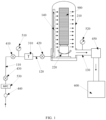
FIG. 1 is a schematic structural diagram of a semiconductor heat treatment device according to an embodiment of the present disclosure; -
FIG. 2 is a schematic structural diagram of a gas conveying pipeline in a semiconductor heat treatment device according to an embodiment of the present disclosure; -
FIG. 3 is another schematic structural diagram of a gas conveying pipeline in a semiconductor heat treatment device according to an embodiment of the present disclosure; -
FIG. 4 is a schematic structural diagram of a gas storage member in a semiconductor heat treatment device according to an embodiment of the present disclosure; -
FIG. 5 is another schematic structural diagram of a gas storage member in a semiconductor heat treatment device according to an embodiment of the present disclosure; and -
FIG. 6 is a flowchart illustrating a control method for a semiconductor heat treatment device according to an embodiment of the present disclosure. -
- 110-gas intake section, 120-communication section, 130-exhaust pipeline, 140-gas conveying pipeline, 141-gas hole,
- 210-process chamber, 220-rotating mechanism,
- 310-gas storage member, 311-first buffer section, 312-straight section, 313-second buffer section, 320-Vacuum Coupling Radius Seal joint, 330-joint connector,
- 410-first valve, 420-second valve, 430-third valve, 440-first pressure regulating valve, 450-second pressure regulating valve,
- 510-first pressure detection element, 520-second pressure detection element, 530-mass flow controller,
- 600-waste gas treatment apparatus,
- 900-wafer.
- In order to make the objectives, technical solutions and advantages of the present disclosure clearer, the technical solutions of the present disclosure are clearly and thoroughly described below in conjunction with the specific embodiments of the present disclosure and the corresponding drawings. Apparently, the embodiments described herein are merely some embodiments of the present disclosure, and do not cover all embodiments. All other embodiments derived by those of ordinary skill in the art from the embodiments described herein without inventive work fall within the scope of the present disclosure.
- The technical solutions provided in each embodiment of the present disclosure are described in detail below with reference to the drawings.
- As shown in
FIG. 1 to FIG. 5 , an embodiment of the present disclosure provides a semiconductor heat treatment device, which can enable awafer 900 and a process gas to interact so as to deposit the process gas on a surface of thewafer 900. The semiconductor heat treatment device specifically includes a gas intake pipeline, anexhaust pipeline 130, agas conveying pipeline 140, aprocess chamber 210, and a gas storage assembly. The gas storage assembly is disposed on the gas intake pipeline. For convenience of description below, the gas intake pipeline is divided into agas intake section 110 and acommunication section 120. The gas storage assembly has a gas storage stage and a gas release stage. In order to ensure that the gas storage assembly is capable of being switched between the gas storage stage and the gas release stage, the gas storage assembly may include agas storage member 310, afirst valve 410, and asecond valve 420. - The
process chamber 210 may provide a process environment and an accommodating space for the processing of thewafer 900, and allow the process gas to be supplied into theprocess chamber 210 to react with thewafer 900. During the processing of thewafer 900, a plurality of semiconductors such as a plurality ofwafers 900 may be accommodated and regularly arranged in theprocess chamber 210. Specifically, the plurality ofwafers 900 may be distributed along a height direction of theprocess chamber 210. Certainly, in order to ensure that the process gas may be deposited on a surface of eachwafer 900, a gap needs to be provided between any twoadjacent wafers 900 among the plurality ofwafers 900. In addition, a bearing mechanism may be disposed in theprocess chamber 210 for bearing the plurality ofwafers 900, and may be specifically a wafer boat. - The process gas may be supplied by a gas source, which may be a gas storage device. In order to ensure safety of the process gas used in the semiconductor processing, the gas source may be a gas supply pipeline, so as to avoid potential safety hazards caused when the process gas is kept in a high pressure state for a long time.
- In a process of conveying the process gas, one end of the
gas intake section 110 of the gas intake pipeline may be communicated with the gas source, and the other end of thegas intake section 110 may be communicated with thegas storage member 310, so as to enable the process gas to be conveyed into thegas storage member 310 through thegas intake section 110. Specifically, thegas intake section 110 may be made of a metal material such as stainless steel, which may also prevent the process gas from reacting with thegas intake section 110 to avoid an adverse effect on the process. Connecting components such as joints and gaskets may be adopted for communication between thegas intake section 110 and each of the gas source and thegas storage member 310, and may ensure reliable sealing connection between thegas intake section 110 and the gas source and between thegas intake section 110 and thegas storage member 310. In addition, all parameters of thegas intake section 110 such as a length and a flow may be determined according to actual needs, and are not limited herein. - Meanwhile, the
first valve 410 is disposed on thegas intake section 110 of the gas intake pipeline, that is, thefirst valve 410 is disposed on a portion of the gas intake pipeline which is located upstream of thegas storage member 310, so as to control a connection state and a disconnection state of thegas intake section 110 and thegas storage member 310. In a case where thefirst valve 410 is closed, thegas intake section 110 is disconnected from thegas storage member 310, and the process gas output by the gas source cannot be conveyed into thegas storage member 310 through thegas intake section 110; correspondingly, in a case where thefirst valve 410 is open, thegas intake section 110 and thegas storage member 310 are communicated with each other, and the process gas output by the gas source may be conveyed into thegas storage member 310 through thegas intake section 110. Specifically, thefirst valve 410 may be a solenoid valve or a pneumatic valve. - As stated above, the
process chamber 210 may provide the process environment for thewafer 900. On such basis, in order to ensure that the process gas can be conveyed into theprocess chamber 210 and can be uniformly conveyed to a region where the plurality ofwafers 900 are located, optionally, thegas conveying pipeline 140 is disposed inside theprocess chamber 210, so as to convey the process gas to different regions of theprocess chamber 210. Meanwhile, in order to ensure as much as possible that the process gas can be conveyed to any position in theprocess chamber 210 through thegas conveying pipeline 140, thegas conveying pipeline 140 may be disposed parallel to a central axis of theprocess chamber 210. The central axis of the process chamber is along the height direction of theprocess chamber 210, that is, along an arrangement direction of thewafers 900 in theprocess chamber 210. - More specifically, the
gas conveying pipeline 140 may be provided with a plurality ofgas holes 141 each configured to convey the process gas into theprocess chamber 210, and the plurality ofgas holes 141 are distributed along the arrangement direction of the plurality ofwafers 900 accommodated in theprocess chamber 210, so that a gas conveying region formed by the plurality ofgas holes 141 may correspond to the region where the plurality ofwafers 900 are located, and thegas conveying pipeline 140 may cover the region where the plurality ofwafers 900 are located as much as possible, so as to enable the process gas to act on eachwafer 900. - As shown in
FIG. 1 , thegas storage member 310 is communicated with one end of thegas conveying pipeline 140 through thecommunication section 120 of the gas intake pipeline, so as to ensure that the process gas in thegas storage member 310 can be conveyed into theprocess chamber 210 through thecommunication section 120 and thegas conveying pipeline 140. Thecommunication section 120 may be also made of a metal material, and both thegas storage member 310 and thegas conveying pipeline 140 are hermetically connected to thecommunication section 120. - Certainly, in order to enable the process gas in the
gas storage member 310 to be conveyed into theprocess chamber 210 in a controllable manner, as shown inFIG. 1 , thesecond valve 420 is disposed on thecommunication section 120, that is, thesecond valve 420 is disposed on a portion of the gas intake pipeline which is located downstream of thegas storage member 310, so that connection and disconnection between thegas storage member 310 and theprocess chamber 210 may be controlled by opening and closing thesecond valve 420. Specifically, in a case where thesecond valve 420 is open, the process gas in thegas storage member 310 may be conveyed into theprocess chamber 210 through thecommunication section 120; and in a case where thesecond valve 420 is closed, the process gas in thegas storage member 310 cannot be conveyed into theprocess chamber 210. Thesecond valve 420 may be a solenoid valve or a pneumatic valve. - In addition, in order to discharge a waste gas generated during the process out of the
process chamber 210 during the process and after the process, in the semiconductor heat treatment device provided in the embodiments of the present disclosure, theprocess chamber 210 is further communicated with one end of theexhaust pipeline 130, and the other end of theexhaust pipeline 130 is configured to be communicated with a wastegas processing apparatus 600. In this way, if a pressure of theprocess chamber 210 exceeds a preset pressure range during the process, the gas in theprocess chamber 210 may be extracted with the wastegas processing apparatus 600, so as to reduce the pressure in theprocess chamber 210 to the preset pressure range and improve a process effect. Certainly, the waste gas in theprocess chamber 210 may be also extracted with the wastegas treatment apparatus 600 after the process is completed. - In order to minimize an adverse effect of the waste gas in the
exhaust pipeline 130 on a process carried out in theprocess chamber 210, optionally, theexhaust pipeline 130 may be provided with a secondpressure regulating valve 450, and connection and disconnection of the wastegas treatment apparatus 600 and theprocess chamber 210 may be enabled with the secondpressure regulating valve 450. In addition, in order to accurately perceive a specific pressure situation in theprocess chamber 210, theexhaust pipeline 130 may be further provided with a secondpressure detection element 520 located between theprocess chamber 210 and the secondpressure regulating valve 450, so that whether the pressure in theprocess chamber 210 is within the preset pressure range may be determined with the secondpressure detection element 520, and the pressure in theprocess chamber 210 may be regulated with the secondpressure regulating valve 450 in a case where the pressure in theprocess chamber 210 exceeds the preset pressure range, thereby ensuring that an operation pressure in theprocess chamber 210 is always within the preset pressure range and improving the process effect. - Based on the above semiconductor heat treatment device, when there is a need to carry out a process by the semiconductor heat treatment device, the plurality of
wafers 900 may be first placed in theprocess chamber 210, and the process environment in theprocess chamber 210 may be processed through theexhaust pipeline 130 and the wastegas treatment apparatus 600 to meet process requirements. Then, thefirst valve 410 may be opened and thesecond valve 420 may be closed, so that the process gas supplied by the gas source may be conveyed into thegas storage member 310 through thegas intake section 110 for storage. As the process gas is continuously conveyed into thegas storage member 310, a pressure of the process gas in thegas storage member 310 is also increased. The amount of the process gas required for performing the corresponding process on the plurality ofwafers 900 may be obtained according to parameters such as the number and sizes of thewafers 900 in theprocess chamber 210 together with a specific type of the corresponding process. Then, in a case where a gas storage amount of the process gas in thegas storage member 310 reaches a first preset value, thefirst valve 410 is closed, and thesecond valve 420 is opened, so that the process gas stored in thegas storage member 310 may be quickly conveyed into thegas conveying pipeline 140 through thecommunication section 120 under the action of the pressure of the process gas itself, and may be conveyed into theprocess chamber 210 through the plurality ofgas holes 141 in thegas conveying pipeline 140. Certainly, it needs to be ensured that the process gas conveyed into thegas conveying pipeline 140 from thegas storage member 310 through thecommunication section 120 has a high pressure, so as to ensure an equal gas pressure of eachgas hole 141 in the gas conveying pipeline, thereby making the process gas conveyed into theprocess chamber 210 through thegas conveying pipeline 140 be uniform in amount at all positions in theprocess chamber 210. For achieving such objective, the gas storage amount of the process gas remaining in thegas storage member 310 may be controlled, and thegas storage member 310 is controlled with thesecond valve 420 to stop supplying the gas to the process chamber in a case where a gas pressure in thegas storage member 310 is slightly greater than or equal to a gas pressure in theprocess chamber 210. - Specifically, a device such as a flowmeter may be adopted to measure the amount of the process gas conveyed into the
gas storage member 310 through thegas intake section 110 within a preset time period; or, parameters such as the pressure of the process gas in thegas storage member 310 when the amount of the process gas stored in thegas storage member 310 meets the process requirements may be obtained according to parameters such as a kind of the process gas and a volume of thegas storage member 310, and then the pressure of the process gas in thegas storage member 310 may be detected with the pressure detection element, so as to indirectly obtain the amount of the process gas stored in thegas storage member 310. - In the semiconductor heat treatment device provided in the embodiments of the present disclosure, one end of the gas intake pipeline is communicated with the gas source, and the other end of the gas intake pipeline is communicated with the gas conveying pipeline located in the process chamber. Specifically, the gas source is communicated with the
gas storage member 310 through thegas intake section 110 of the gas intake pipeline, thegas storage member 310 is communicated with thegas conveying pipeline 140 located in theprocess chamber 210 through thecommunication section 120 of the gas intake pipeline, and thegas conveying pipeline 140 is parallel to the central axis of theprocess chamber 210, and is provided with the plurality ofgas holes 141 each configured to convey the process gas to theprocess chamber 210. Theprocess chamber 210 is further communicated with theexhaust pipeline 130 to ensure an unobstructed gas path, and theexhaust pipeline 130 may be further configured to stabilize the operating pressure in theprocess chamber 210. - In the above semiconductor heat treatment device, in a case where the gas storage amount of the process gas in the
gas storage member 310 reaches the first preset value, thegas storage member 310 supplies the process gas to theprocess chamber 210 through the gas intake pipeline and thegas conveying pipeline 140 in sequence, and the process gas in thegas storage member 310 can be quickly diffused into thegas conveying pipeline 140 through thecommunication section 120 under the action of the pressure of the process gas itself. Since the process gas in thegas storage member 310 has a certain pressure, the process gas after being output from thegas storage member 310 can be reliably moved to agas hole 141 in thegas conveying pipeline 140 which is far away from thegas storage member 310, so that it can be ensured that the process gas can be uniformly output through the plurality ofgas holes 141 of thegas conveying pipeline 140, thereby ensuring that a process result of eachwafer 900 meets the process requirements. - As stated above, the amount of the process gas stored in the
gas storage member 310 may be obtained by measuring the flow or the pressure. In a specific implementation, the semiconductor heat treatment device further includes a firstpressure detection element 510, which is disposed on the gas intake pipeline and located between thefirst valve 410 and thegas storage member 310, that is, disposed on thegas intake section 110 of the gas intake pipeline. The firstpressure detection element 510 is configured to detect the gas in thegas storage member 310. Specifically, the firstpressure detection element 510 may be a pressure gauge or a pressure sensor. Under the condition that the parameters such as the volume of thegas storage member 310 and the kind of the process gas are known, the amount of the process gas stored in thegas storage member 310 may be indirectly obtained according to a measurement value of the firstpressure detection element 510. - In another embodiment of the present disclosure, the semiconductor heat treatment device further includes a
mass flow controller 530, which is installed on thegas intake section 110. Under the action of the mass flow controller (MFC) 530, the amount of the process gas conveyed into thegas storage member 310 through thegas intake section 110 within the preset time period may be obtained more accurately, which may improve accuracy of a measurement value of the amount of the process gas in thegas storage member 310. - In order to further improve the accuracy of the measurement value of the amount of the process gas in the
gas storage member 310, optionally, the firstpressure detection element 510 together with themass flow controller 530 may be disposed in the semiconductor heat treatment device, so as to obtain the amount of the process gas stored in thegas storage member 310 from multiple dimensions, thereby improving the accuracy of the measurement value to the greatest extent. - In order to further facilitate controlling the conveying process of the process gas, optionally, the semiconductor heat treatment device further includes a
third valve 430, which is installed between thefirst valve 410 and themass flow controller 530. Thethird valve 430 may be closed when there is no need to convey the process gas, so as to improve safety of the conveying of the process gas. - In addition, the semiconductor heat treatment device may further include a first
pressure regulating valve 440, which is installed on thegas intake section 110. The firstpressure regulating valve 440 is located between themass flow controller 530 and the gas source, so that a conveying pressure of the process gas in thegas intake section 110 may be regulated with the firstpressure regulating valve 440 when the process gas needs to be conveyed to the semiconductor heat treatment device during the process, so as to improve the stability of the conveying of the process gas. - In order to further improve uniformity in the amount of the process gas conveyed to each of the plurality of
wafers 900 in theprocess chamber 210, structures and/or arrangement of the gas holes 141 in thegas conveying pipeline 140 may be designed to realize a substantially equal amount of the process gas conveyed to eachwafer 900. - Optionally, as shown in
FIG. 2 , the plurality ofgas holes 141 are distributed along the central axis of theprocess chamber 210, and gas-conveying section areas of the plurality ofgas holes 141 gradually increase along a gas conveying direction (as shown by the arrow inFIG. 2 ) of thegas conveying pipeline 140, that is, each gas hole has a different gas-conveying section area, and the farther thegas hole 141 is away from thecommunication section 120, the larger the gas-conveying section area of thegas hole 141 is. The gas-conveying section area of eachgas hole 141 is an area of a cross section of thegas hole 141 perpendicular to an axial direction of thegas hole 141, and may represent a gas conveying capability of thegas hole 141; and the larger the gas-conveying section area is, the better the gas conveying capability of thegas hole 141 is. By adopting such technical solution, even if there is a difference in the pressures of the process gas at thedifferent gas holes 141, since thegas hole 141 farther way from thegas storage member 310 has the larger gas-conveying section area, an adverse effect of a lower pressure of the process gas at thegas hole 141 farther way from thegas storage member 310 on a gas output amount of thegas hole 141 farther way from thegas storage member 310 may be compensated, so as to ensure as much as possible that the plurality ofgas holes 141 are the same in gas output amount. In addition, by adopting the above technical solution, an equal distance may be provided between any two adjacent gas holes 141. - As shown in
FIG. 3 , in another embodiment of the present disclosure, the plurality ofgas holes 141 are distributed along the central axis of theprocess chamber 210, and a distance between any adjacent twogas holes 141 among the plurality ofgas holes 141 gradually decreases along a gas conveying direction (as shown by the arrow inFIG. 3 ) of thegas conveying pipeline 140. That is, in a process of arranging the gas holes 141 in thegas conveying pipeline 140, the gas holes 141 at positions farther away from thecommunication section 120 are denser. In this way, even if the gas pressures at the gas holes 141 at the positions farther away from thecommunication section 120 are lower due to the larger distances between the gas holes 141 at the positions farther away from thecommunication section 120 and thegas storage member 310, an adverse effect of the lower gas pressures may be compensated by increasing the density of the gas holes 141, thereby ensuring the substantially equal amount of the process gas conveyed to each of the plurality ofwafers 900. In addition, in the semiconductor heat treatment device provided in the embodiments of the present disclosure, eachgas hole 141 may have the same radius, so as to reduce difficulty in processing the gas holes 141. - In another embodiment of the present disclosure, the plurality of
gas holes 141 are distributed along the central axis of theprocess chamber 210, gas-conveying section areas of the plurality ofgas holes 141 gradually increase along a gas conveying direction of thegas conveying pipeline 140, and meanwhile, a distance between any twoadjacent gas holes 141 among the plurality ofgas holes 141 gradually decreases, so as to improve the uniformity in gas conveying amount of the plurality ofgas holes 141 to the greatest extent. Certainly, specific parameters of the gas-conveying section areas of the gas holes 141 and the distance between any twoadjacent gas holes 141 may be adaptively adjusted in practical applications, so as to ensure a substantially equal gas conveying amount of each of the plurality of gas holes 141. - As stated above, the
gas storage member 310 may store the process gas to pressurize the process gas therein, so as to improve a diffusion capability and a diffusion speed of the process gas, thereby improving uniformity of the process gas at the different regions in theprocess chamber 210. On such basis, in order to improve storage and release performance of the process gas of thegas storage member 310, optionally, as shown inFIG. 4 andFIG. 5 , thegas storage member 310 includes afirst buffer section 311, astraight section 312, and asecond buffer section 313, which are sequentially connected in series along a gas intake direction (i.e., the directions from left to right shown inFIG. 4 andFIG. 5 ), and thefirst buffer section 311, thestraight section 312, and thesecond buffer section 313 form thegas storage member 310 together. In a process of assembling thegas storage member 310, one end of thegas intake section 110 is configured to be communicated with the gas source, the other end of thegas intake section 110 is communicated with one end of thefirst buffer section 311 away from thestraight section 312, one end of thesecond buffer section 313 away from thestraight section 312 is communicated with one end of thecommunication section 120, and the other end of thecommunication section 120 is communicated with thegas conveying pipeline 140. - Specifically, each of the
first buffer section 311, thesecond buffer section 313, and thestraight section 312 may be made of a material with a high structural strength such as metal, so as to improve gas storage performance of thegas storage member 310. Moreover, thefirst buffer section 311 and thesecond buffer section 313 may be fixedly connected to thestraight section 312 by welding. In order to improve connection reliability of thefirst buffer section 311, thesecond buffer section 313, and thestraight section 312, optionally, thefirst buffer section 311, thestraight section 312, and thesecond buffer section 313 may be integrally formed. - In addition, along the gas intake direction of the
gas storage member 310, an area of a section of thefirst buffer section 311 which is perpendicular to the gas intake direction (i.e., the directions from left to right shown inFIG. 4 andFIG. 5 ) gradually increases, and an area of a section of thesecond buffer section 313 which is perpendicular to the gas intake direction (i.e., the directions from left to right shown inFIG. 4 andFIG. 5 ) gradually decreases, so that thefirst buffer section 311 and thesecond buffer section 313 have smooth structures, and the gas may be gradually diffused after entering thegas storage member 310 through thefirst buffer section 311, which reduces difficulty in conveying the gas, and the gas may be gradually compressed and organized at thesecond buffer section 313 while being conveyed into thegas conveying pipeline 140 from thesecond buffer section 313 through thecommunication section 120, which improves the diffusion speed and a diffusion effect of the process gas. - In addition, under the condition that both the
first buffer section 311 and thesecond buffer section 313 have the smooth structures, the process gas may be prevented from being blocked when flowing in thegas storage member 310 as much as possible, which improves a flow capability of the process gas. Correspondingly, in order to further prevent the process gas from being blocked when flowing from thefirst buffer section 311 to thesecond buffer section 313, a shape of a projection of thestraight section 312 along the gas intake direction may be made to be the same as a shape of a section of thestraight section 312 which is perpendicular to the gas intake direction, that is, thestraight section 312 is a straight structural member as a whole, which may prevent the process gas from being blocked by thestraight section 312 when flowing in thegas storage member 310, thereby ensuring flow smoothness of the process gas. - More specifically, the
straight section 312 may be a cylindrical structural member, and correspondingly, an end surface of thefirst buffer section 311 which is connected to thestraight section 312 and an end surface of thesecond buffer section 313 which is connected to thestraight section 312 are both circular structures, which may further improve flow performance of the process gas in thegas storage member 310, and prevent the process gas from being deposited at corners of thegas storage member 310, thereby increasing utilization of the process gas. - As stated above, in the semiconductor heat treatment device provided in the embodiments of the present disclosure, joints and gaskets may be adopted to connect the
first buffer section 311 to thegas intake section 110 and connect thesecond buffer section 313 to thecommunication section 120, so as to realize good sealing performance between those sections. In another embodiment of the present disclosure, a Vacuum Coupling Radius Seal joint 320 (i.e., a VCR joint) may be adopted for hermetic connection between thegas storage member 310 and thegas intake section 110 and/or between thegas storage member 310 and thecommunication section 120, and the VCR joint 320 may ensure good sealing performance between thegas storage member 310 and thegas intake section 110 and between thegas storage member 310 and thecommunication section 120, so as to prevent leakage of the process gas and improve process safety. Certainly, the VCR joint 320 may be adopted to connect any two components, such as thecommunication section 120 and thegas conveying pipeline 140 or theprocess chamber 210 and theexhaust pipeline 130, so as to ensure high connection reliability and good sealing performance between any two connected components in the semiconductor heat treatment device. - In addition, a
joint connector 330 may be adopted to assist in connecting thegas storage member 310 to theVCR joint 320. Specifically, after theVCR joint 320 is inserted into thejoint connector 330, an end of thegas storage member 310 is welded to thejoint connector 330, thereby connecting the VCR joint 320 to thegas storage member 310 into a whole. - As stated above, the semiconductor heat treatment device may include the bearing mechanism for bearing the plurality of
wafers 900 thereon. In order to further improve uniformity in deposition amount of the process gas on eachwafer 900, optionally, the semiconductor heat treatment device provided in the embodiments of the present disclosure may further include arotating mechanism 220, which may specifically be a rotating motor. Therotating mechanism 220 is installed at theprocess chamber 210, and the bearing mechanism is disposed in theprocess chamber 210 and installed on therotating mechanism 220, so that therotating mechanism 220 may drive the bearing mechanism to rotate, and a rotating direction is specifically a direction around the arrangement direction of the plurality ofwafers 900. - For example, the plurality of
wafers 900 may be arranged along the height direction of theprocess chamber 210, and therotating mechanism 220 may drive the bearing mechanism to rotate along a direction around the height direction of theprocess chamber 210, that is, driving the bearing mechanism to rotate in a horizontal plane. Under the action of therotating mechanism 220, thewafers 900 may rotate relative to the gas holes 141 on thegas conveying pipeline 140, which may ensure a uniform deposition amount of the process gas at any position of thewafers 900 and improve the process effect of thewafers 900. - In order to ensure that the process gas may be conveyed from the gas source into the
gas storage member 310, the process gas needs to have a certain pressure while being conveyed, that is, the process gas in thegas conveying pipeline 140 also has a certain pressure. A gas can be easily liquefied when being pressurized, and some kinds of process gases have certain viscosity after being liquefied, which is not favorable to the conveying of the process gas. Accordingly, based on a fact that the pressure of the process gas in thegas storage member 310 is higher, the semiconductor heat treatment device provided in the embodiments of the present disclosure further includes a first heating mechanism and a second heating mechanism, the first heating mechanism is disposed at a heating pipeline for heating thegas intake section 110 to a first preset temperature, and the second heating mechanism is disposed at thegas storage member 310 for heating thegas storage member 310 to a second preset temperature. Under the effects of the first heating mechanism and the second heating mechanism, liquefaction difficulty of the process gas in thegas intake section 110 and thegas storage member 310 is increased, so as to avoid a phenomenon that the process gas is liquefied during the conveying process to the greatest extent, thereby increasing conveying efficiency of the process gas. - In addition, since the pressure of the process gas in the
gas storage member 310 is higher than the pressure of the process gas in thegas intake section 110, the second preset temperature may be set to be higher than the first preset temperature, so as to ensure that the process gas in thegas storage member 310 is not liquefied. Specifically, each of the first heating mechanism and the second heating mechanism may be a heating device such as heating wires, and the first heating mechanism may wrap around thegas intake section 110 for heating thegas intake section 110. Correspondingly, the second heating mechanism may wrap around thegas storage member 310 for heating thegas storage member 310. Such arrangement of the first heating mechanism and the second heating mechanism has low difficulty. Specific values of the first preset temperature and the second preset temperature may be determined according to a kind of a process gas actually used in practical applications. Taking the process gas being SiH2Cl2 as an example, the first preset temperature may be 40°C, and the second preset temperature may be between 120°C and 150°C. - Based on the above semiconductor heat treatment device, an embodiment of the present disclosure further provides a control method for a semiconductor heat treatment device, so as to control the above semiconductor heat treatment device with the control method. As shown in
FIG. 6 , the control method includes:
S1, introducing a gas into a gas storage assembly through a gas intake pipeline. - That is, after a process is started, a portion of the gas intake pipeline (i.e., a gas intake section 110) which is located between a gas source and a
gas storage member 310 is communicated, so that a process gas output by the gas source is temporarily stored in thegas storage member 310 of the gas storage assembly, and a pressure of the process gas may be generated in thegas storage member 310. - After step S1, the control method for the semiconductor heat treatment device provided in the embodiment of the present disclosure further includes:
S2, supplying the process gas to aprocess chamber 210 in a case where a gas storage amount of the gas storage assembly reaches a first preset value. - Specifically, the amount of the process gas required for performing a corresponding process on a plurality of
wafers 900 may be obtained according to parameters such as the number and sizes of thewafers 900 in theprocess chamber 210 together with a specific type of the corresponding process. Then, in a case where the gas storage amount of the process gas in thegas storage member 310 reaches the first preset value, afirst valve 410 is closed, and asecond valve 420 is opened, so that the process gas stored in thegas storage member 310 may be quickly conveyed into agas conveying pipeline 140 through acommunication section 120 under the action of the pressure of the process gas itself, and may be conveyed into theprocess chamber 210 through a plurality ofgas holes 141 in thegas conveying pipeline 140, thereby completing conveying of the process gas. In this way, it can be ensured that gas output amounts of thegas conveying pipeline 140 corresponding to the plurality ofwafers 900 are substantially the same, thereby improving uniformity of a process result. - In addition, during the use of the semiconductor heat treatment device provided in the embodiments of the present disclosure, a specific value of the first preset value of the process gas in the
gas storage member 310 may be tested. Specifically, a specific value may be first set for the first preset value of the process gas in thegas storage member 310, then the semiconductor heat treatment device is controlled with the control method provided in the embodiment of the present disclosure to perform gas conveying, a plurality ofwafers 900 to be tested are subjected to a deposition process, and thicknesses and uniformity of deposition layers on all thewafers 900 are detected to obtain a corresponding relationship between the first preset value and the process result. Then, by changing the specific value of the first preset value and correspondingly completing the deposition process on thewafers 900, a plurality of sets of corresponding data may be obtained, and a corresponding relationship between the first preset value of the storage amount of the process gas in thegas storage member 310 and the specific parameters such as the sizes and the number of thewafers 900 may be obtained based on the plurality of sets of corresponding data. When the semiconductor heat treatment device is used subsequently, the specific value of the first preset value may be correspondingly determined according to the above corresponding relationship and parameters such as the number and sizes ofwafers 900 to be processed, so as to ensure a good process effect of thewafers 900. - In some alternative embodiments, the control method further includes:
- heating a
gas intake section 110 to a first preset temperature; and - heating the gas storage assembly to a second preset temperature, with the second preset temperature being higher than the first preset temperature.
- In order to ensure that the process gas may be conveyed from the gas source into the
gas storage member 310, the process gas needs to have a certain pressure while being conveyed, that is, the process gas in thegas conveying pipeline 140 also has a certain pressure. A gas can be easily liquefied when being pressurized, and some kinds of process gases have certain viscosity after being liquefied, which is not favorable to the conveying of the process gas. Accordingly, based on a fact that the pressure of the process gas in thegas storage member 310 is higher, liquefaction difficulty of the process gas in thegas intake section 110 and thegas storage member 310 may be increased by heating thegas intake section 110 to the first preset temperature and heating thegas storage member 310 to the second preset temperature according to an embodiment of the present disclosure, so as to avoid a phenomenon that the process gas is liquefied during the conveying process to the greatest extent, thereby increasing conveying efficiency of the process gas. - In addition, since the pressure of the process gas in the
gas storage member 310 is higher than the pressure of the process gas in thegas intake section 110, the second preset temperature may be set to be higher than the first preset temperature, so as to ensure that the process gas in thegas storage member 310 is not liquefied. Specific values of the first preset temperature and the second preset temperature may be determined according to a kind of a process gas actually used in practical applications. Taking the process gas being SiH2Cl2 as an example, the first preset temperature may be 40°C, and the second preset temperature may be between 120°C and 150°C. - The above embodiments of the present disclosure focus on the differences between the embodiments, and different optimization features of the embodiments can be combined to form better embodiments as long as the different optimization features are not contradictory, which will not be described in detail here for conciseness of the description.
- The description above is merely of the embodiments of the present disclosure, but is not intended to limit the present disclosure. Various modifications and changes may be made to the present disclosure by those of ordinary skill in the art. Any modification, equivalent replacement and improvement made within the spirit and principle of the present disclosure should be included in the scope of the appended claims of the present disclosure.
Claims (11)
- A semiconductor heat treatment device, comprising a process chamber, a gas intake pipeline, a gas conveying pipeline, and an exhaust pipeline, one end of the gas intake pipeline is communicated with a gas source, the other end of the gas intake pipeline is communicated with the gas conveying pipeline located in the process chamber, the gas conveying pipeline is parallel to a central axis of the process chamber, the gas conveying pipeline is provided with a plurality of gas holes, and each of the plurality of gas holes is configured to convey a process gas into the process chamber; and the exhaust pipeline is communicated with the process chamber, wherein a gas storage assembly is disposed on the gas intake pipeline, and is configured to supply the process gas to the process chamber through the gas intake pipeline and the gas conveying pipeline in sequence in a case where a gas storage amount reaches a first preset value.
- The semiconductor heat treatment device of claim 1, wherein the plurality of gas holes are distributed along the central axis, and gas-conveying section areas of the plurality of gas holes gradually increase along a gas conveying direction of the gas conveying pipeline.
- The semiconductor heat treatment device of claim 1, wherein the plurality of gas holes are distributed along the central axis, and a distance between any two adjacent gas holes among the plurality of gas holes gradually decreases along a gas conveying direction of the gas conveying pipeline.
- The semiconductor heat treatment device of claim 1, wherein the gas storage assembly comprises a gas storage member, a first valve, and a second valve, the first valve is disposed on a portion of the gas intake pipeline which is located upstream of the gas storage member, and the second valve is disposed on a portion of the gas intake pipeline which is located downstream of the gas storage member;the gas intake pipeline comprises a gas intake section and a communication section; the gas storage member comprises a first buffer section, a straight section, and a second buffer section, which are sequentially connected in series along a gas intake direction of the gas storage member, one end of the gas intake section is configured to be communicated with the gas source, the other end of the gas intake section is communicated with one end of the first buffer section away from the straight section, one end of the second buffer section away from the straight section is communicated with one end of the communication section, and the other end of the communication section is communicated with the gas conveying pipeline;along the gas intake direction of the gas storage member, an area of a section of the first buffer section which is perpendicular to the gas intake direction gradually increases, and an area of a section of the second buffer section which is perpendicular to the gas intake direction gradually decreases; anda shape of a projection of the straight section along the gas intake direction is the same as a shape of a section of the straight section which is perpendicular to the gas intake direction.
- The semiconductor heat treatment device of claim 4, wherein the first buffer section is hermetically connected to the gas intake section through a Vacuum Coupling Radius Seal joint, and the second buffer section is hermetically connected to the communication section through a Vacuum Coupling Radius Seal joint.
- The semiconductor heat treatment device of claim 1, further comprising a first heating mechanism and a second heating mechanism, wherein the gas intake pipeline comprises a gas intake section located upstream of the gas storage assembly and a communication section located downstream of the gas storage assembly, and the first heating mechanism is disposed on the gas intake section for heating the gas intake section; and the second heating mechanism is disposed on the gas storage assembly for heating the gas storage assembly.
- The semiconductor heat treatment device of claim 1, further comprising a first pressure detection element, which is configured to detect a gas pressure in the gas storage assembly.
- The semiconductor heat treatment device of claim 1, further comprising a mass flow controller, which is installed on the gas intake pipeline.
- The semiconductor heat treatment device of claim 1, further comprising a bearing mechanism and a rotating mechanism, wherein the rotating mechanism is installed at the process chamber, the bearing mechanism is disposed in the process chamber, and is installed at the rotating mechanism, the rotating mechanism is configured to drive the bearing mechanism to rotate around the central axis, and the bearing mechanism is configured to bear a plurality of wafers.
- A control method for a semiconductor heat treatment device, comprising:introducing a gas into a gas storage assembly through a gas intake pipeline; andsupplying a process gas to a process chamber in a case where a gas storage amount of the gas storage assembly reaches a first preset value.
- The control method for the semiconductor heat treatment device of claim 10, wherein the semiconductor heat treatment device further comprises a first heating mechanism and a second heating mechanism, the gas intake pipeline comprises a gas intake section located upstream of the gas storage assembly and a communication section located downstream of the gas storage assembly, and the first heating mechanism is disposed on the gas intake section for heating the gas intake section; and the second heating mechanism is disposed on the gas storage assembly for heating the gas storage assembly; and
the control method further comprises:heating the gas intake section to a first preset temperature; andheating the gas storage assembly to a second preset temperature; wherein the second preset temperature is higher than the first preset temperature.
Applications Claiming Priority (2)
| Application Number | Priority Date | Filing Date | Title |
|---|---|---|---|
| CN202210600893.8A CN114823428A (en) | 2022-05-30 | 2022-05-30 | Semiconductor heat treatment apparatus and control method thereof |
| PCT/CN2023/095228 WO2023231805A1 (en) | 2022-05-30 | 2023-05-19 | Semiconductor heat treatment device and control method therefor |
Publications (2)
| Publication Number | Publication Date |
|---|---|
| EP4535407A1 true EP4535407A1 (en) | 2025-04-09 |
| EP4535407A4 EP4535407A4 (en) | 2026-06-24 |
Family
ID=82519385
Family Applications (1)
| Application Number | Title | Priority Date | Filing Date |
|---|---|---|---|
| EP23814989.2A Pending EP4535407A4 (en) | 2022-05-30 | 2023-05-19 | Semiconductor heat treatment device and control method therefor |
Country Status (6)
| Country | Link |
|---|---|
| EP (1) | EP4535407A4 (en) |
| JP (1) | JP7835898B2 (en) |
| KR (1) | KR20250002553A (en) |
| CN (1) | CN114823428A (en) |
| TW (1) | TWI851219B (en) |
| WO (1) | WO2023231805A1 (en) |
Families Citing this family (14)
| Publication number | Priority date | Publication date | Assignee | Title |
|---|---|---|---|---|
| US12221696B2 (en) | 2022-05-27 | 2025-02-11 | Applied Materials, Inc. | Process kits and related methods for processing chambers to facilitate deposition process adjustability |
| US12354855B2 (en) | 2022-05-27 | 2025-07-08 | Applied Materials, Inc. | Process kits and related methods for processing chambers to facilitate deposition process adjustability |
| CN114823428A (en) * | 2022-05-30 | 2022-07-29 | 北京北方华创微电子装备有限公司 | Semiconductor heat treatment apparatus and control method thereof |
| US12428731B2 (en) | 2022-07-12 | 2025-09-30 | Applied Materials, Inc. | Flow guide structures and heat shield structures, and related methods, for deposition uniformity and process adjustability |
| US12696707B2 (en) | 2022-07-12 | 2026-07-28 | Applied Materials, Inc. | Batch processing apparatus, systems, and related methods and structures for epitaxial deposition operations |
| US12243761B2 (en) | 2022-10-27 | 2025-03-04 | Applied Materials, Inc. | Detection and analysis of substrate support and pre-heat ring in a process chamber via imaging |
| US12467144B2 (en) | 2022-10-27 | 2025-11-11 | Applied Materials, Inc. | Methods of correlating zones of processing chambers, and related systems and methods |
| CN115928048A (en) * | 2022-11-28 | 2023-04-07 | 江苏天芯微半导体设备有限公司 | Semiconductor equipment, gas pipeline thereof and heating method of process gas |
| US12428753B2 (en) | 2022-12-14 | 2025-09-30 | Applied Materials, Inc. | Lift assemblies, and related methods and components, for substrate processing chambers |
| CN120603995A (en) | 2023-01-26 | 2025-09-05 | 应用材料公司 | Purification system for cleaning the wafer backside of a ring susceptor |
| US12696715B2 (en) | 2023-10-20 | 2026-07-28 | Applied Materials, Inc. | Fin structures, plate apparatus, and related methods, process kits, and processing chambers for growth rates and process uniformity |
| US12540400B2 (en) | 2023-11-02 | 2026-02-03 | Applied Materials, Inc. | Multi-flow gas circuits, processing chambers, and related apparatus and methods for semiconductor manufacturing |
| CN118167518A (en) * | 2024-04-24 | 2024-06-11 | 东风商用车有限公司 | A dust-cleaning air filter, a vehicle and a dust-cleaning method for the dust-cleaning air filter |
| CN120758856B (en) * | 2025-06-09 | 2026-01-09 | 北京集成电路装备创新中心有限公司 | Uniform flow assembly and vertical furnace |
Family Cites Families (19)
| Publication number | Priority date | Publication date | Assignee | Title |
|---|---|---|---|---|
| JP3919208B2 (en) * | 1997-08-01 | 2007-05-23 | シーケーディ株式会社 | Process gas supply unit |
| JP2000097398A (en) | 1998-09-24 | 2000-04-04 | Nippon Sanso Corp | Gas container inner surface treatment method |
| TW550307B (en) | 2000-04-19 | 2003-09-01 | Getters Spa | A process for the purification of organometallic compounds or heteroatomic organic compounds with hydrogenated getter alloys |
| US20030111013A1 (en) * | 2001-12-19 | 2003-06-19 | Oosterlaken Theodorus Gerardus Maria | Method for the deposition of silicon germanium layers |
| KR20030081144A (en) * | 2002-04-11 | 2003-10-17 | 가부시키가이샤 히다치 고쿠사이 덴키 | Vertical semiconductor manufacturing apparatus |
| JP3947126B2 (en) | 2002-04-11 | 2007-07-18 | 株式会社日立国際電気 | Semiconductor manufacturing equipment |
| JP4939864B2 (en) | 2006-07-25 | 2012-05-30 | 東京エレクトロン株式会社 | Gas supply apparatus, gas supply method, thin film forming apparatus cleaning method, thin film forming method, and thin film forming apparatus |
| JP6128969B2 (en) | 2013-06-03 | 2017-05-17 | 株式会社日立国際電気 | Substrate processing apparatus, semiconductor device manufacturing method, and program |
| JP2015073021A (en) | 2013-10-03 | 2015-04-16 | 三井造船株式会社 | Atomic layer deposition device and atomic layer deposition method |
| JP6413293B2 (en) * | 2014-03-27 | 2018-10-31 | 東京エレクトロン株式会社 | Film forming method and storage medium |
| JP6447338B2 (en) * | 2015-04-16 | 2019-01-09 | 東京エレクトロン株式会社 | Vertical heat treatment equipment |
| JP6678489B2 (en) * | 2016-03-28 | 2020-04-08 | 東京エレクトロン株式会社 | Substrate processing equipment |
| CN109817545B (en) * | 2017-11-22 | 2021-07-16 | 台湾积体电路制造股份有限公司 | Semiconductor wafer processing system and method for processing semiconductor wafers |
| CN111837223B (en) | 2018-03-22 | 2025-02-25 | 株式会社国际电气 | Substrate processing device, method for manufacturing semiconductor device, and recording medium |
| CN108690972A (en) * | 2018-08-06 | 2018-10-23 | 长江存储科技有限责任公司 | Gas injection tube and film deposition device for film deposition device |
| CN210349787U (en) * | 2019-09-23 | 2020-04-17 | 长江存储科技有限责任公司 | Semiconductor manufacturing equipment |
| CN111455349B (en) * | 2020-04-01 | 2022-07-22 | 北京北方华创微电子装备有限公司 | Semiconductor processing equipment |
| CN111725108B (en) * | 2020-06-23 | 2024-05-17 | 北京北方华创微电子装备有限公司 | Semiconductor processing equipment |
| CN114823428A (en) * | 2022-05-30 | 2022-07-29 | 北京北方华创微电子装备有限公司 | Semiconductor heat treatment apparatus and control method thereof |
-
2022
- 2022-05-30 CN CN202210600893.8A patent/CN114823428A/en active Pending
-
2023
- 2023-05-19 KR KR1020247038285A patent/KR20250002553A/en active Pending
- 2023-05-19 TW TW112118747A patent/TWI851219B/en active
- 2023-05-19 EP EP23814989.2A patent/EP4535407A4/en active Pending
- 2023-05-19 JP JP2024568531A patent/JP7835898B2/en active Active
- 2023-05-19 WO PCT/CN2023/095228 patent/WO2023231805A1/en not_active Ceased
Also Published As
| Publication number | Publication date |
|---|---|
| CN114823428A (en) | 2022-07-29 |
| TW202346631A (en) | 2023-12-01 |
| JP2025516815A (en) | 2025-05-30 |
| TWI851219B (en) | 2024-08-01 |
| EP4535407A4 (en) | 2026-06-24 |
| WO2023231805A1 (en) | 2023-12-07 |
| JP7835898B2 (en) | 2026-03-25 |
| KR20250002553A (en) | 2025-01-07 |
Similar Documents
| Publication | Publication Date | Title |
|---|---|---|
| TWI851219B (en) | Semiconductor heat treatment equipment and its control method | |
| TWI830157B (en) | Gas supply control device | |
| US20110256003A1 (en) | Dry vacuum pump | |
| US20080295963A1 (en) | Gas supply system and gas supply accumulation unit of semiconductor manufacturing apparatus | |
| KR101669689B1 (en) | Apparatus and method for controlling flow rate of liquid, and storage medium | |
| CN112359423B (en) | Pressure control device and semiconductor processing equipment | |
| US20220325801A1 (en) | Control valve, substrate processing apparatus, method of manufacturing semiconductor device, and recording medium | |
| CN113805619A (en) | Pressure control system and control method | |
| KR20140108677A (en) | Pressurizing apparatus, substrate bonding apparatus, and bonded substrates | |
| US20250093890A1 (en) | Composition mixture control of efem environment | |
| KR20160004974A (en) | Exhaust and load port having therof | |
| US20240219258A1 (en) | Leakage detection apparatus, substrate processing apparatus, substrate processing method, method of manufacturing semiconductor device and non-transitory computer-readable recording medium | |
| US12046456B2 (en) | Inspection method of plasma processing apparatus | |
| US20230417326A1 (en) | Multi-layer and multi-ringed seals for preventing permeation and leak-by of fluid | |
| CN221566369U (en) | Wafer transfer system and epitaxy process equipment | |
| CN223176207U (en) | Gas control structure | |
| CN219342268U (en) | Gas circuit system for sputtering coating equipment and sputtering coating equipment | |
| US12540695B2 (en) | Conversion pipe arrangement, substrate processing apparatus, method of processing substrate, and method of manufacturing semiconductor device | |
| CN222352094U (en) | Process medium transport structure and semiconductor process equipment | |
| WO2020049900A1 (en) | Method and equipment for supplying fluorine-gas-containing gas | |
| US20250066909A1 (en) | Seal structure, chamber, substrate processing apparatus, and method of installing seal material | |
| JP5138195B2 (en) | Heat transfer gas supply mechanism, heat transfer gas supply method, substrate processing apparatus, and substrate processing method | |
| KR20180101199A (en) | Gas introduction mechanism and heat treatment apparatus | |
| CN120967324A (en) | Gas transmission equipment, semiconductor process equipment and gas control methods | |
| WO2024226137A1 (en) | System, method, and apparatus for flow tuning |
Legal Events
| Date | Code | Title | Description |
|---|---|---|---|
| STAA | Information on the status of an ep patent application or granted ep patent |
Free format text: STATUS: THE INTERNATIONAL PUBLICATION HAS BEEN MADE |
|
| PUAI | Public reference made under article 153(3) epc to a published international application that has entered the european phase |
Free format text: ORIGINAL CODE: 0009012 |
|
| STAA | Information on the status of an ep patent application or granted ep patent |
Free format text: STATUS: REQUEST FOR EXAMINATION WAS MADE |
|
| 17P | Request for examination filed |
Effective date: 20241122 |
|
| AK | Designated contracting states |
Kind code of ref document: A1 Designated state(s): AL AT BE BG CH CY CZ DE DK EE ES FI FR GB GR HR HU IE IS IT LI LT LU LV MC ME MK MT NL NO PL PT RO RS SE SI SK SM TR |
|
| DAV | Request for validation of the european patent (deleted) | ||
| DAX | Request for extension of the european patent (deleted) | ||
| REG | Reference to a national code |
Ref country code: DE Ref legal event code: R079 Free format text: PREVIOUS MAIN CLASS: H01L0021670000 Ipc: H10P0072000000 |
|
| A4 | Supplementary search report drawn up and despatched |
Effective date: 20260528 |
|
| RIC1 | Information provided on ipc code assigned before grant |
Ipc: H10P 72/00 20260101AFI20260521BHEP |