EP4535358A1 - Row decoder circuit and corresponding method of operation - Google Patents
Row decoder circuit and corresponding method of operation Download PDFInfo
- Publication number
- EP4535358A1 EP4535358A1 EP24200308.5A EP24200308A EP4535358A1 EP 4535358 A1 EP4535358 A1 EP 4535358A1 EP 24200308 A EP24200308 A EP 24200308A EP 4535358 A1 EP4535358 A1 EP 4535358A1
- Authority
- EP
- European Patent Office
- Prior art keywords
- node
- cascode
- supply
- voltage
- circuit
- Prior art date
- Legal status (The legal status is an assumption and is not a legal conclusion. Google has not performed a legal analysis and makes no representation as to the accuracy of the status listed.)
- Pending
Links
Images
Classifications
-
- G—PHYSICS
- G11—INFORMATION STORAGE
- G11C—STATIC STORES
- G11C8/00—Arrangements for selecting an address in a digital store
- G11C8/08—Word line control circuits, e.g. drivers, boosters, pull-up circuits, pull-down circuits, precharging circuits, for word lines
-
- G—PHYSICS
- G11—INFORMATION STORAGE
- G11C—STATIC STORES
- G11C16/00—Erasable programmable read-only memories
- G11C16/02—Erasable programmable read-only memories electrically programmable
- G11C16/06—Auxiliary circuits, e.g. for writing into memory
- G11C16/08—Address circuits; Decoders; Word-line control circuits
-
- G—PHYSICS
- G11—INFORMATION STORAGE
- G11C—STATIC STORES
- G11C16/00—Erasable programmable read-only memories
- G11C16/02—Erasable programmable read-only memories electrically programmable
- G11C16/06—Auxiliary circuits, e.g. for writing into memory
- G11C16/10—Programming or data input circuits
- G11C16/102—External programming circuits, e.g. EPROM programmers; In-circuit programming or reprogramming; EPROM emulators
-
- G—PHYSICS
- G11—INFORMATION STORAGE
- G11C—STATIC STORES
- G11C16/00—Erasable programmable read-only memories
- G11C16/02—Erasable programmable read-only memories electrically programmable
- G11C16/06—Auxiliary circuits, e.g. for writing into memory
- G11C16/26—Sensing or reading circuits; Data output circuits
- G11C16/28—Sensing or reading circuits; Data output circuits using differential sensing or reference cells, e.g. dummy cells
Definitions
- the description relates to row decoder circuits and corresponding methods of operation.
- Row decoders may be applied to non-volatile memories (NVM) where the state of a memory cell can be changed applying a programming current to the cell itself, such as phase-change memories (PCM), spin-torque magnetoresistive random-access memories (ST-MRAM), and resistive random-access memories (RRAM).
- NVM non-volatile memories
- PCM phase-change memories
- ST-MRAM spin-torque magnetoresistive random-access memories
- RRAM resistive random-access memories
- Document US 11289158 B2 assigned to companies of the STMicroelectronics group, discloses a non-volatile memory device that includes a row decoder.
- the row decoder includes a pull-down stage (e.g., operating as a NAND gate) and a pull-up stage (e.g., a p-channel transistor) for each word line of the memory.
- the pull-down stage is configured to tie the word line to ground (i.e., to select the word line) and the pull-up stage is configured to tie the word line to a selectable supply voltage (e.g., the supply voltage being 2 V during read operation and 4.8 V during write operation).
- the row decoder further includes a CMOS inverter configured to drive the pull-up stage.
- the CMOS inverter is supplied between the supply voltage and a selectable shifted ground voltage (e.g., the shifted ground voltage being 0 V during read operation and 2.4 V during write operation) .
- the input node of the CMOS inverter is biased by a current generator (e.g., a current mirror) and can be tied to ground via one or more selection transistors coupled in series with two cascode n-channel transistors.
- a current generator e.g., a current mirror
- the input node of the CMOS inverter switches between 0 V (selected word line) and 1.8 V (unselected word line).
- the input node of the CMOS inverter switches between 0 V (selected word line) and 4.8 V (unselected word line). Therefore, transistors in the CMOS inverter and in the current generator are dimensioned for 5 V rating.
- the voltage domain of the row decoder circuit may be between ground voltage (e.g., 0 V) and a relatively high voltage (e.g., 4.8 V or 5 V, the higher value of the selectable supply voltage), and the transistors are conventionally designed (e.g., sized) for such a voltage rating.
- ground voltage e.g., 0 V
- a relatively high voltage e.g., 4.8 V or 5 V, the higher value of the selectable supply voltage
- the transistors are conventionally designed (e.g., sized) for such a voltage rating.
- Such sizing implies thick gate oxide and/or large area occupation, and the fabrication of such high-voltage transistors also requires dedicated manufacturing steps and dedicated masks that make the manufacturing costs increase.
- An object of one or more embodiments is to contribute in providing such improved row decoder circuits that can handle high voltages (e.g., in the range of 0 V to about 5 V) without implementing high-voltage rating transistors, but implementing (only) low-voltage rating transistors (e.g., in the range of 0 V to about 2.5 V).
- such an object can be achieved by a row decoder circuit having the features set forth in the claims that follow.
- One or more embodiments may relate to a corresponding method of operation.
- a row decoder circuit includes at least one input node configured to receive at least one row selection signal and an output node configured for coupling to a word line of a memory device.
- the row decoder includes a pull-down circuit coupled between the word line and a ground node at ground voltage.
- the pull-down circuit is configured to selectively couple the word line to the ground node in response to the at least one row selection signal being asserted.
- the row decoder includes a pull-up circuit coupled between the word line and a supply node that provides a selectable supply voltage.
- the pull-up circuit is configured to selectively couple the word line to the supply node in response to a deselection signal being de-asserted.
- the row decoder includes an inverter circuit supplied between the supply node and a shifted ground node that provides a selectable reference voltage.
- the inverter circuit is configured to receive as input a control signal from a control node and produce the deselection signal.
- the row decoder includes a current generator circuit configured to source a biasing current to the control node.
- the row decoder includes a further pull-down circuit coupled between the control node and the ground node. The further pull-down circuit is configured to selectively couple the control node to the ground node in response to the at least one row selection signal being asserted.
- the further pull-down circuit includes a first cascode n-channel transistor, a cascode p-channel transistor, a second cascode n-channel transistor, and at least one selection transistor having their conductive channels arranged in series between the control node and the ground node.
- the at least one selection transistor is controlled by the at least one row selection signal.
- One or more embodiments may thus provide a row decoder circuit able to manage high voltages (e.g., in the range of 0 V to 5 V) without resorting to high-voltage rating devices but using (only) low-voltage rating devices (e.g., in the range of 0 V to 2.5 V).
- high voltages e.g., in the range of 0 V to 5 V
- low-voltage rating devices e.g., in the range of 0 V to 2.5 V.
- a method of operating a row decoder circuit includes:
- references to "an embodiment” or “one embodiment” in the framework of the present description is intended to indicate that a particular configuration, structure, or characteristic described in relation to the embodiment is included in at least one embodiment.
- phrases such as “in an embodiment” or “in one embodiment” that may be present in one or more points of the present description do not necessarily refer to one and the same embodiment.
- particular configurations, structures, or characteristics may be combined in any adequate way in one or more embodiments.
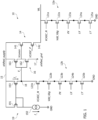
- Figure 1 is a circuit block diagram exemplary of a row decoder circuit 10 as is known, for instance, from document US 11289158 B2 cited in the foregoing.
- the row decoder circuit 10 is configured to control (i.e., select and deselect) a word line WL of a memory device.
- the row decoder 10 includes a pull-down stage 12a and a pull-up stage 14 for each word line WL of the memory.
- the pull-down stage 12a is configured to tie the word line WL to ground GND (i.e., to select the word line) and the pull-up stage 14 is configured to tie the word line WL to a supply node 15 that provides a selectable (or variable) supply voltage shifted_supply (i.e., to deselect the word line).
- the supply voltage shifted_supply may be, for instance, 2 V during read operation and 4.8 V during write operation.
- the pull-down stage 12a may include five n-channel MOS transistors arranged in series between the word line WL and ground GND, and specifically, starting from the word line WL and moving towards ground GND: a first cascode transistor 121a, a second cascode transistor 122a, a first selection transistor 123a, a second selection transistor 124a, and a third selection transistor 125a.
- Transistor 121a has a drain terminal coupled to the word line WL, a gate terminal configured to receive a first (positive) cascode voltage VCASC_N, and a source terminal coupled to the drain terminal of transistor 122a.
- Transistor 122a has a drain terminal coupled to the source terminal of transistor 121a, a gate terminal configured to receive a second (positive) cascode voltage Vdd_fdig, and a source terminal coupled to the drain terminal of transistor 123a.
- Transistor 123a has a drain terminal coupled to the source terminal of transistor 122a, a gate terminal configured to receive a first selection signal PX, and a source terminal coupled to the drain terminal of transistor 124a.
- Transistor 124a has a drain terminal coupled to the source terminal of transistor 123a, a gate terminal configured to receive a second selection signal LX, and a source terminal coupled to the drain terminal of transistor 125a.
- Transistor 125a has a drain terminal coupled to the source terminal of transistor 124a, a gate terminal configured to receive a third selection signal LY, and a source terminal coupled to ground GND.
- the pull-up stage 14 may include two p-channel MOS transistors arranged in series between the supply node 15 and the word line WL, and specifically, starting from the supply node 15 and moving towards the word line WL: a deselection transistor 141, and a cascode transistor 142.
- Transistor 141 has a source terminal coupled to the supply node 15, a gate terminal configured to receive a deselection signal Vcomm, and a drain terminal coupled to the source terminal of transistor 142.
- Transistor 142 has a source terminal coupled to the drain terminal of transistor 141, a gate terminal configured to receive a cascode voltage VCASC_P, and a drain terminal coupled to the word line WL.
- the row decoder 10 further includes a CMOS inverter 16 configured to produce signal Vcomm to drive transistor 141.
- the CMOS inverter 16 is supplied between node 15 (at voltage shifted_supply ) and a shifted ground node 17 that provides a selectable (or variable) shifted ground voltage shifted_gnd.
- the shifted ground voltage shifted_gnd may be, for instance, 0 V during read operation and 2.4 V during write operation (i.e., equal to the reference voltage of ground GND during read operation, and equal to half of the supply voltage shifted_supply during write operation).
- inverter 16 may include a p-channel MOS transistor 161 and an n-channel MOS transistor 162 arranged in series between nodes 15 and 17.
- Transistor 161 has a source terminal coupled to the supply node 15, a gate terminal coupled to a deselection control node 18, and a drain terminal coupled to the drain terminal of transistor 162 and to the gate terminal of transistor 141.
- Transistor 162 has a drain terminal coupled to the drain terminal of transistor 161 and to the gate terminal of transistor 141, a gate terminal coupled to node 18, and a source terminal coupled to the shifted ground node 17.
- the deselection control node 18 (i.e., the input of the CMOS inverter 16) is biased by a current generator 19 (e.g., a current mirror) that sources a current I 1 to it.
- the current mirror 19 may include a first branch including a diode-connected p-channel MOS transistor 191 arranged in series with a current-sinking element 192 between the supply node 15 and ground GND, and a second branch including a mirroring p-channel MOS transistor 193 arranged between the supply node 15 and the control node 18 and having a gate terminal coupled to the gate terminal of transistor 191 to source current I 1 to node 18.
- the mirroring ratio of transistors 191 and 193 may be unitary.
- the deselection control node 18 can be tied to ground GND via a pull-down stage 12b that replicates the structure and operation of the pull-down stage 12a.
- the pull-down stage 12b includes two cascode n-channel transistors 121b, 122b coupled in series with a plurality of (e.g., three) selection transistors 123b, 124b, 125b that receive the same signals VCASC_N, Vdd_fdig, PX, LX, LY as the pull-down stage 12a.
- a switching control voltage V 1 is produced at node 18 by the operation of the generator 19 and the pull-down stage 12b.
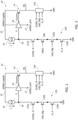
- Figure 2 shows the same architecture of Figure 1 in a simplified view, where the internal structure of the pull-down stage 12a, the pull-up stage 14, the CMOS inverter 16 and the current generator 19 is not shown in detail. Further, concerning the pull-down stage 12b, the selection transistors 123b, 124b and 125b are shown as a single transistor 12xb and the reference ln_lv is used to indicate collectively the selection signals PX, LX, LY.
- transistors 161, 162 and 193 are subject to a 5 V (or 4.8 V) voltage swing, and are dimensioned accordingly (e.g., for 5 V rating). Such sizing may imply thick gate oxide and/or large area occupation, and the fabrication of such high-voltage transistors may also require dedicated manufacturing steps and dedicated masks that make the manufacturing costs increase.
- one or more embodiments relate to an improved row decoder circuit that does not rely on high-voltage rating transistors.
- Figure 3 is a circuit block diagram exemplary of a row decoder circuit 10' according to one or more embodiments.
- the row decoder 10' includes substantially all the circuit components described with reference to the decoder architecture of Figures 1 and 2 , plus an additional p-channel MOS cascode transistor 300 arranged in series with the cascode transistors 121b and 122b in the pull-down stage 12b' (i.e., between node 18 and ground GND).
- Transistor 300 is configured to receive, at its gate terminal, a cascode voltage VNEG.
- the cascode transistor 300 may be arranged between transistors 121b and 122b.
- transistor 300 has a source terminal coupled to the source terminal of transistor 121b, a drain terminal coupled to the drain terminal of transistor 122b, and a gate terminal configured to receive the cascode voltage VNEG.
- the cascode voltage VNEG may be produced by a control circuit of the memory device.
- the cascode voltage VNEG may be, for instance, 0 V minus a threshold Vth during read operation (i.e., the ground voltage GND minus the threshold Vth) and 2.4 V minus the threshold Vth during write operation (i.e., half of the supply voltage shifted_supply minus the threshold Vth).
- the threshold Vth (the voltage threshold of transistor 300) may be equal to 0.4 V.
- the cascode voltage VNEG is equal to -0.4 V during read operation and equal to 2.0 V during write operation. Therefore, at least during read operation, the cascode voltage VNEG is negative.
- the voltages may assume the following exemplary values, depending on whether the memory operates in read mode or write mode, and depending on whether the word line WL has to be selected or deselected.
- the selection signals ln_lv e.g., PX, LX, PY
- the cascode voltage VNEG is negative (e.g., -0.4 V)
- the supply voltage shifted_supply is 2 V
- the ground voltage shifted_gnd is 0 V; consequently, voltage V 1 at node 18 is 0 V, voltage Vcomm is 2 V, and the word line WL is pulled down to ground GND (0 V).
- the selection signals ln_lv (e.g., PX, LX, PY ) are logic low (e.g., 0 V)
- the cascode voltage VNEG is negative (e.g., - 0.4 V)
- the supply voltage shifted_supply is 2 V
- the ground voltage shifted_gnd is 0 V; consequently, voltage V 1 at node 18 is 2 V, voltage Vcomm is 0 V, and the word line WL is pulled up to the supply voltage shifted_supply (2 V).
- the selection signals ln_lv (e.g., PX, LX, PY ) are logic high (e.g., 1 V), the cascode voltage VNEG is positive (e.g., 2 V), the supply voltage shifted_supply is 4.8 V, and the ground voltage shifted_gnd is 2.4 V; consequently, voltage V 1 at node 18 is 2.4 V, voltage Vcomm is 4.8 V, and the word line WL is pulled down to ground GND (0 V).
- the selection signals ln_lv (e.g., PX, LX, PY ) are logic low (e.g., 0 V)
- the cascode voltage VNEG is positive (e.g., 2 V)
- the supply voltage shifted_supply is 4.8 V
- the ground voltage shifted_gnd is 2.4 V; consequently, voltage V 1 at node 18 is 4.8 V, voltage Vcomm is 2.4 V, and the word line WL is pulled up to the supply voltage shifted_supply (4.8 V) .
- voltage V 1 at node 18 switches between 0 V (in case the word line WL is selected) and 1.8 V (in case the word line WL is deselected) during read operation, and it switches between 2.4 V (in case the word line WL is selected) and 4.8 V (in case the word line WL is deselected) during write operation. Therefore, the voltage swing of node 18 is limited to less than 2.5 V.
- transistors 161, 162 and 193 are subject to a maximum voltage swing of 2.5 V, and are dimensioned accordingly (e.g., for 2.5 V rating).
- Such sizing implies a thinner gate oxide, a lower area occupation and /or a higher switching speed compared to previous solutions.
- the fabrication of low-voltage transistors implies less manufacturing steps and less masks compared to previous solutions, which result in lower manufacturing costs.
- row decoder circuits as disclosed herein may be used in the control circuits of a memory.
- One or more embodiments as exemplified herein may thus be advantageous insofar as they facilitate managing "high" voltages (e.g., in the range of 0 V to 5 V) without resorting to high-voltage rating devices but using (only) low-voltage rating devices (e.g., in the range of 0 V to 2.5 V).
- "high" voltages e.g., in the range of 0 V to 5 V
- low-voltage rating devices e.g., in the range of 0 V to 2.5 V.
Landscapes
- Engineering & Computer Science (AREA)
- Microelectronics & Electronic Packaging (AREA)
- Read Only Memory (AREA)
Abstract
In a row decoder circuit (10') an input node receives a row selection signal (ln_lv) and an output node is coupled to a word line (WL) of a memory device. A pull-down circuit (12a) coupled between the word line (WL) and a ground node (GND) at ground voltage selectively couples the word line to the ground node in response to the row selection signal (ln_lv) being asserted. A pull-up circuit (14) coupled between the word line and a supply node (15) that provides a selectable supply voltage (shifted_supply) selectively couples the word line to the supply node in response to a deselection signal (Vcomm) being de-asserted. An inverter circuit (16) supplied between the supply node and a shifted ground node (17) that provides a selectable reference voltage (shifted_gnd) receives as input a control signal (V1 ) from a control node (18) and produces the deselection signal. A current generator (19) sources a biasing current (I1 ) to the control node. A further pull-down circuit (121b, 122b, 300, 12xb, 12b') coupled between the control node and the ground node selectively couples the control node to the ground node in response to the row selection signal being asserted. The further pull-down circuit (12b') comprises a first cascode n-channel transistor (121b), a cascode p-channel transistor (300), a second cascode n-channel transistor (122b), and at least one selection transistor (12xb) having their conductive channels arranged in series between the control node and the ground node, wherein the selection transistor is controlled by the row selection signal.
Description
- The description relates to row decoder circuits and corresponding methods of operation.
- Row decoders may be applied to non-volatile memories (NVM) where the state of a memory cell can be changed applying a programming current to the cell itself, such as phase-change memories (PCM), spin-torque magnetoresistive random-access memories (ST-MRAM), and resistive random-access memories (RRAM).
- Document
US 11289158 B2 - Other documents possibly of interest in the field of the invention include
US 2014/0269140 A1 ,US 2023/0062498 A1 ,US 2016/0240260 A1 , andUS 6885250 B1 . - In such known memory applications, the voltage domain of the row decoder circuit may be between ground voltage (e.g., 0 V) and a relatively high voltage (e.g., 4.8 V or 5 V, the higher value of the selectable supply voltage), and the transistors are conventionally designed (e.g., sized) for such a voltage rating. Such sizing implies thick gate oxide and/or large area occupation, and the fabrication of such high-voltage transistors also requires dedicated manufacturing steps and dedicated masks that make the manufacturing costs increase.
- Therefore, there is a need in the art to provide improved row decoder circuits that do not rely on high-voltage rating transistors.
- An object of one or more embodiments is to contribute in providing such improved row decoder circuits that can handle high voltages (e.g., in the range of 0 V to about 5 V) without implementing high-voltage rating transistors, but implementing (only) low-voltage rating transistors (e.g., in the range of 0 V to about 2.5 V).
- According to one or more embodiments, such an object can be achieved by a row decoder circuit having the features set forth in the claims that follow.
- One or more embodiments may relate to a corresponding method of operation.
- The claims are an integral part of the technical teaching provided herein in respect of the embodiments.
- According to an aspect of the present description, a row decoder circuit includes at least one input node configured to receive at least one row selection signal and an output node configured for coupling to a word line of a memory device. The row decoder includes a pull-down circuit coupled between the word line and a ground node at ground voltage. The pull-down circuit is configured to selectively couple the word line to the ground node in response to the at least one row selection signal being asserted. The row decoder includes a pull-up circuit coupled between the word line and a supply node that provides a selectable supply voltage. The pull-up circuit is configured to selectively couple the word line to the supply node in response to a deselection signal being de-asserted. The row decoder includes an inverter circuit supplied between the supply node and a shifted ground node that provides a selectable reference voltage. The inverter circuit is configured to receive as input a control signal from a control node and produce the deselection signal. The row decoder includes a current generator circuit configured to source a biasing current to the control node. The row decoder includes a further pull-down circuit coupled between the control node and the ground node. The further pull-down circuit is configured to selectively couple the control node to the ground node in response to the at least one row selection signal being asserted. The further pull-down circuit includes a first cascode n-channel transistor, a cascode p-channel transistor, a second cascode n-channel transistor, and at least one selection transistor having their conductive channels arranged in series between the control node and the ground node. The at least one selection transistor is controlled by the at least one row selection signal.
- One or more embodiments may thus provide a row decoder circuit able to manage high voltages (e.g., in the range of 0 V to 5 V) without resorting to high-voltage rating devices but using (only) low-voltage rating devices (e.g., in the range of 0 V to 2.5 V).
- According to another aspect of the present description, a method of operating a row decoder circuit according to one or more embodiments includes:
- receiving at least one row selection signal at at least one input node of the row decoder;
- selectively coupling a word line to a ground node of the row decoder in response to the at least one row selection signal being asserted;
- selectively coupling the word line to a supply node of the row decoder in response to a deselection signal being de-asserted;
- receiving, at an input of an inverter circuit of the row decoder, a control signal from a control node of the row decoder and producing, at an output of the inverter circuit, the deselection signal;
- sourcing a biasing current to the control node; and
- selectively coupling the control node to the ground node in response to the at least one row selection signal being asserted.
- One or more embodiments will now be described, by way of example, with reference to the annexed figures, wherein:
-
Figure 1 is a circuit block diagram exemplary of a row decoder circuit; -
Figure 2 is a simplified circuit block diagram exemplary of the row decoder circuit ofFigure 1 ; and -
Figure 3 is a circuit block diagram exemplary of a row decoder circuit according to one or more embodiments of the present description. - In the ensuing description, one or more specific details are illustrated, aimed at providing an in-depth understanding of examples of embodiments of this description. The embodiments may be obtained without one or more of the specific details, or with other methods, components, materials, etc. In other cases, known structures, materials, or operations are not illustrated or described in detail so that certain aspects of embodiments will not be obscured.
- Reference to "an embodiment" or "one embodiment" in the framework of the present description is intended to indicate that a particular configuration, structure, or characteristic described in relation to the embodiment is included in at least one embodiment. Hence, phrases such as "in an embodiment" or "in one embodiment" that may be present in one or more points of the present description do not necessarily refer to one and the same embodiment. Moreover, particular configurations, structures, or characteristics may be combined in any adequate way in one or more embodiments.
- The headings/references used herein are provided merely for convenience and hence do not define the extent of protection or the scope of the embodiments.
- Throughout the figures annexed herein, unless the context indicates otherwise, like parts or elements are indicated with like references/numerals and a corresponding description will not be repeated for the sake of brevity.
- By way of introduction to the detailed description of exemplary embodiments, reference may be made to
Figures 1 and2 , discussed in the following. -
Figure 1 is a circuit block diagram exemplary of arow decoder circuit 10 as is known, for instance, from documentUS 11289158 B2 row decoder circuit 10 is configured to control (i.e., select and deselect) a word line WL of a memory device. To this effect, therow decoder 10 includes a pull-downstage 12a and a pull-upstage 14 for each word line WL of the memory. The pull-downstage 12a is configured to tie the word line WL to ground GND (i.e., to select the word line) and the pull-upstage 14 is configured to tie the word line WL to asupply node 15 that provides a selectable (or variable) supply voltage shifted_supply (i.e., to deselect the word line). The supply voltage shifted_supply may be, for instance, 2 V during read operation and 4.8 V during write operation. - The pull-down
stage 12a may include five n-channel MOS transistors arranged in series between the word line WL and ground GND, and specifically, starting from the word line WL and moving towards ground GND: afirst cascode transistor 121a, asecond cascode transistor 122a, afirst selection transistor 123a, asecond selection transistor 124a, and athird selection transistor 125a.Transistor 121a has a drain terminal coupled to the word line WL, a gate terminal configured to receive a first (positive) cascode voltage VCASC_N, and a source terminal coupled to the drain terminal oftransistor 122a.Transistor 122a has a drain terminal coupled to the source terminal oftransistor 121a, a gate terminal configured to receive a second (positive) cascode voltage Vdd_fdig, and a source terminal coupled to the drain terminal oftransistor 123a.Transistor 123a has a drain terminal coupled to the source terminal oftransistor 122a, a gate terminal configured to receive a first selection signal PX, and a source terminal coupled to the drain terminal oftransistor 124a.Transistor 124a has a drain terminal coupled to the source terminal oftransistor 123a, a gate terminal configured to receive a second selection signal LX, and a source terminal coupled to the drain terminal oftransistor 125a.Transistor 125a has a drain terminal coupled to the source terminal oftransistor 124a, a gate terminal configured to receive a third selection signal LY, and a source terminal coupled to ground GND. - The pull-up
stage 14 may include two p-channel MOS transistors arranged in series between thesupply node 15 and the word line WL, and specifically, starting from thesupply node 15 and moving towards the word line WL: adeselection transistor 141, and acascode transistor 142.Transistor 141 has a source terminal coupled to thesupply node 15, a gate terminal configured to receive a deselection signal Vcomm, and a drain terminal coupled to the source terminal oftransistor 142.Transistor 142 has a source terminal coupled to the drain terminal oftransistor 141, a gate terminal configured to receive a cascode voltage VCASC_P, and a drain terminal coupled to the word line WL. - The
row decoder 10 further includes aCMOS inverter 16 configured to produce signal Vcomm to drivetransistor 141. TheCMOS inverter 16 is supplied between node 15 (at voltage shifted_supply) and a shiftedground node 17 that provides a selectable (or variable) shifted ground voltage shifted_gnd. The shifted ground voltage shifted_gnd may be, for instance, 0 V during read operation and 2.4 V during write operation (i.e., equal to the reference voltage of ground GND during read operation, and equal to half of the supply voltage shifted_supply during write operation). In particular,inverter 16 may include a p-channel MOS transistor 161 and an n-channel MOS transistor 162 arranged in series betweennodes Transistor 161 has a source terminal coupled to thesupply node 15, a gate terminal coupled to adeselection control node 18, and a drain terminal coupled to the drain terminal oftransistor 162 and to the gate terminal oftransistor 141.Transistor 162 has a drain terminal coupled to the drain terminal oftransistor 161 and to the gate terminal oftransistor 141, a gate terminal coupled tonode 18, and a source terminal coupled to the shiftedground node 17. - The deselection control node 18 (i.e., the input of the CMOS inverter 16) is biased by a current generator 19 (e.g., a current mirror) that sources a current I1 to it. For instance, the
current mirror 19 may include a first branch including a diode-connected p-channel MOS transistor 191 arranged in series with a current-sinkingelement 192 between thesupply node 15 and ground GND, and a second branch including a mirroring p-channel MOS transistor 193 arranged between thesupply node 15 and thecontrol node 18 and having a gate terminal coupled to the gate terminal oftransistor 191 to source current I1 tonode 18. The mirroring ratio oftransistors - The
deselection control node 18 can be tied to ground GND via a pull-down stage 12b that replicates the structure and operation of the pull-down stage 12a. In particular, the pull-down stage 12b includes two cascode n-channel transistors selection transistors down stage 12a. - Therefore, a switching control voltage V1 is produced at
node 18 by the operation of thegenerator 19 and the pull-down stage 12b. -
Figure 2 shows the same architecture ofFigure 1 in a simplified view, where the internal structure of the pull-down stage 12a, the pull-upstage 14, theCMOS inverter 16 and thecurrent generator 19 is not shown in detail. Further, concerning the pull-down stage 12b, theselection transistors - During read operation, voltage V1 at
node 18 switches between 0 V (in case the word line WL is selected) and 1.8 V (in case the word line WL is deselected). During write operation, voltage V1 atnode 18 switches between 0 V (in case the word line WL is selected) and 4.8 V (in case the word line WL is deselected). Therefore,transistors - Therefore, one or more embodiments relate to an improved row decoder circuit that does not rely on high-voltage rating transistors.
- In detail,
Figure 3 is a circuit block diagram exemplary of a row decoder circuit 10' according to one or more embodiments. As exemplified inFigure 3 , the row decoder 10' includes substantially all the circuit components described with reference to the decoder architecture ofFigures 1 and2 , plus an additional p-channelMOS cascode transistor 300 arranged in series with thecascode transistors down stage 12b' (i.e., betweennode 18 and ground GND).Transistor 300 is configured to receive, at its gate terminal, a cascode voltage VNEG. - In particular, in one or more embodiments the
cascode transistor 300 may be arranged betweentransistors transistor 300 has a source terminal coupled to the source terminal oftransistor 121b, a drain terminal coupled to the drain terminal oftransistor 122b, and a gate terminal configured to receive the cascode voltage VNEG. - The cascode voltage VNEG may be produced by a control circuit of the memory device. In one or more embodiments, the cascode voltage VNEG may be, for instance, 0 V minus a threshold Vth during read operation (i.e., the ground voltage GND minus the threshold Vth) and 2.4 V minus the threshold Vth during write operation (i.e., half of the supply voltage shifted_supply minus the threshold Vth). For instance, the threshold Vth (the voltage threshold of transistor 300) may be equal to 0.4 V. In this example, the cascode voltage VNEG is equal to -0.4 V during read operation and equal to 2.0 V during write operation. Therefore, at least during read operation, the cascode voltage VNEG is negative.
- Therefore, in the architecture of
Figure 3 , the voltages may assume the following exemplary values, depending on whether the memory operates in read mode or write mode, and depending on whether the word line WL has to be selected or deselected. During read operation, to select the word line WL, the selection signals ln_lv (e.g., PX, LX, PY) are logic high (e.g., 1 V), the cascode voltage VNEG is negative (e.g., -0.4 V), the supply voltage shifted_supply is 2 V, and the ground voltage shifted_gnd is 0 V; consequently, voltage V1 atnode 18 is 0 V, voltage Vcomm is 2 V, and the word line WL is pulled down to ground GND (0 V). During read operation, to deselect the word line WL, the selection signals ln_lv (e.g., PX, LX, PY) are logic low (e.g., 0 V), the cascode voltage VNEG is negative (e.g., - 0.4 V), the supply voltage shifted_supply is 2 V, and the ground voltage shifted_gnd is 0 V; consequently, voltage V1 atnode 18 is 2 V, voltage Vcomm is 0 V, and the word line WL is pulled up to the supply voltage shifted_supply (2 V). During write operation, to select the word line WL, the selection signals ln_lv (e.g., PX, LX, PY) are logic high (e.g., 1 V), the cascode voltage VNEG is positive (e.g., 2 V), the supply voltage shifted_supply is 4.8 V, and the ground voltage shifted_gnd is 2.4 V; consequently, voltage V1 atnode 18 is 2.4 V, voltage Vcomm is 4.8 V, and the word line WL is pulled down to ground GND (0 V). During write operation, to deselect the word line WL, the selection signals ln_lv (e.g., PX, LX, PY) are logic low (e.g., 0 V), the cascode voltage VNEG is positive (e.g., 2 V), the supply voltage shifted_supply is 4.8 V, and the ground voltage shifted_gnd is 2.4 V; consequently, voltage V1 atnode 18 is 4.8 V, voltage Vcomm is 2.4 V, and the word line WL is pulled up to the supply voltage shifted_supply (4.8 V) . - Therefore, in the architecture of
Figure 3 , voltage V1 atnode 18 switches between 0 V (in case the word line WL is selected) and 1.8 V (in case the word line WL is deselected) during read operation, and it switches between 2.4 V (in case the word line WL is selected) and 4.8 V (in case the word line WL is deselected) during write operation. Therefore, the voltage swing ofnode 18 is limited to less than 2.5 V. As a result,transistors - As anticipated, row decoder circuits as disclosed herein may be used in the control circuits of a memory.
- One or more embodiments as exemplified herein may thus be advantageous insofar as they facilitate managing "high" voltages (e.g., in the range of 0 V to 5 V) without resorting to high-voltage rating devices but using (only) low-voltage rating devices (e.g., in the range of 0 V to 2.5 V).
- Without prejudice to the underlying principles, the details and embodiments may vary, even significantly, with respect to what has been described by way of example, without departing from the extent of protection.
- The extent of protection is determined by the annexed claims.
Claims (9)
- A row decoder circuit (10'), comprising:at least one input node configured to receive at least one row selection signal (PX, LX, LY; ln_lv) and an output node configured for coupling to a word line (WL) of a memory device;a pull-down circuit (121a, 122a, 123a, 124a, 125a; 12a) coupled between said word line (WL) and a ground node (GND) at ground voltage, the pull-down circuit (12a) being configured to selectively couple the word line (WL) to the ground node (GND) in response to said at least one row selection signal (ln_lv) being asserted;a pull-up circuit (141, 142; 14) coupled between said word line (WL) and a supply node (15) that provides a selectable supply voltage (shifted_supply), the pull-up circuit (15) being configured to selectively couple the word line (WL) to the supply node (15) in response to a deselection signal (Vcomm) being de-asserted;an inverter circuit (161, 162; 16) supplied between said supply node (15) and a shifted ground node (17) that provides a selectable reference voltage (shifted_gnd), the inverter circuit (16) being configured to receive as input a control signal (V1 ) from a control node (18) and produce said deselection signal (Vcomm);a current generator circuit (191, 192, 193; 19) configured to source a biasing current (I1 ) to said control node (18); anda further pull-down circuit (121b, 122b, 123b, 124b, 125b, 300; 12b') coupled between said control node (18) and the ground node (GND), the further pull-down circuit (12b') being configured to selectively couple the control node (18) to the ground node (GND) in response to said at least one row selection signal (ln_lv) being asserted;wherein the further pull-down circuit (12b') comprises a first cascode n-channel transistor (121b), a cascode p-channel transistor (300), a second cascode n-channel transistor (122b), and at least one selection transistor (123b, 124b, 125b; 12xb) having their conductive channels arranged in series between said control node (18) and the ground node (GND), wherein the at least one selection transistor (12xb) is controlled by said at least one row selection signal (ln_lv).
- A row decoder circuit (10') according to claim 1, wherein:said first cascode n-channel transistor (121b) has a conductive channel arranged between said control node (18) and a first cascode node;said cascode p-channel transistor (300) has a conductive channel arranged between said first cascode node and a second cascode node;said second cascode n-channel transistor (122b) has a conductive channel arranged between said second cascode node and a third cascode node; andsaid at least one selection transistor (123b, 124b, 125b; 12xb) has a conductive channel arranged between said third cascode node and the ground node (GND).
- A row decoder circuit (10') according to claim 1 or claim 2, wherein said cascode p-channel transistor (300) has a control terminal configured to receive a cascode control voltage (VNEG), and wherein the row decoder circuit (10') comprises a memory control circuit configured to set said cascode control voltage (VNEG) to a negative value during read operation of said memory device.
- A row decoder circuit (10') according to claim 3, wherein said negative value of the cascode control voltage (VNEG) is equal to ground voltage minus a threshold, said threshold being preferably in the range of 0.3 V to 0.5 V, more preferably equal to 0.4 V.
- A row decoder circuit (10') according to any of the previous claims, wherein said cascode p-channel transistor (300) has a control terminal configured to receive a cascode control voltage (VNEG), and wherein the row decoder circuit (10') comprises a memory control circuit configured to set said cascode control voltage (VNEG) to a positive value during write operation of said memory device.
- A row decoder circuit (10') according to claim 5, wherein said positive value of the cascode control voltage (VNEG) is equal to half of said selectable supply voltage (shifted_supply) minus a threshold, said threshold being preferably in the range of 0.3 V to 0.5 V, more preferably equal to 0.4 V.
- A row decoder circuit (10') according to any of the previous claims, comprising a memory control circuit configured to:during read operation of said memory device, set said selectable supply voltage (shifted_supply) to a first supply value and set said selectable reference voltage (shifted_gnd) to said ground voltage; andduring write operation of said memory device, set said selectable supply voltage (shifted_supply) to a second supply value, the second supply value being higher than the first supply value, and set said selectable reference voltage (shifted_gnd) to half of said second supply value.
- A row decoder circuit (10') according to claim 7, wherein said first supply value is equal to 2 V and said second supply value is equal to 4.8 V.
- A method of operating a row decoder circuit (10') according to any of the previous claims, the method comprising:receiving at least one row selection signal (PX, LX, LY; ln_lv) at said at least one input node;selectively coupling said word line (WL) to said ground node (GND) in response to said at least one row selection signal (ln_lv) being asserted;selectively coupling said word line (WL) to said supply node (15) in response to a deselection signal (Vcomm) being de-asserted;receiving, at an input of said inverter circuit (16), a control signal (V1 ) from a control node (18) and producing, at an output of said inverter circuit (16), said deselection signal (Vcomm);sourcing a biasing current (I1 ) to said control node (18); andselectively coupling the control node (18) to the ground node (GND) in response to said at least one row selection signal (ln_lv) being asserted.
Applications Claiming Priority (1)
| Application Number | Priority Date | Filing Date | Title |
|---|---|---|---|
| IT102023000020436A IT202300020436A1 (en) | 2023-10-03 | 2023-10-03 | ROW DECODER CIRCUIT AND CORRESPONDING OPERATING PROCEDURE |
Publications (1)
| Publication Number | Publication Date |
|---|---|
| EP4535358A1 true EP4535358A1 (en) | 2025-04-09 |
Family
ID=89068805
Family Applications (1)
| Application Number | Title | Priority Date | Filing Date |
|---|---|---|---|
| EP24200308.5A Pending EP4535358A1 (en) | 2023-10-03 | 2024-09-13 | Row decoder circuit and corresponding method of operation |
Country Status (4)
| Country | Link |
|---|---|
| US (1) | US20250111878A1 (en) |
| EP (1) | EP4535358A1 (en) |
| CN (1) | CN119763636A (en) |
| IT (1) | IT202300020436A1 (en) |
Citations (5)
| Publication number | Priority date | Publication date | Assignee | Title |
|---|---|---|---|---|
| US6885250B1 (en) | 2002-11-22 | 2005-04-26 | Advanced Micro Devices, Inc. | Cascode amplifier circuit for generating and maintaining a fast, stable and accurate bit line voltage |
| US20140269140A1 (en) | 2013-03-14 | 2014-09-18 | Padmaraj Sanjeevarao | Non-volatile memory (nvm) with word line driver/decoder using a charge pump voltage |
| US20160240260A1 (en) | 2015-01-21 | 2016-08-18 | Silicon Storage Technology, Inc. | Flash Memory System Using Complementary Voltage Supplies |
| US20210183442A1 (en) * | 2019-12-16 | 2021-06-17 | Stmicroelectronics S.R.L. | Non-volatile memory device including a row decoder with a pull-up stage |
| US20230062498A1 (en) | 2021-08-31 | 2023-03-02 | Micron Technology, Inc. | Deck-level signal development cascodes |
Family Cites Families (3)
| Publication number | Priority date | Publication date | Assignee | Title |
|---|---|---|---|---|
| JP2002501654A (en) * | 1997-05-30 | 2002-01-15 | ミクロン テクノロジー,インコーポレイテッド | 256Meg dynamic random access memory |
| KR100746626B1 (en) * | 2006-06-30 | 2007-08-08 | 주식회사 하이닉스반도체 | Semiconductor memory device |
| US7940550B2 (en) * | 2009-09-14 | 2011-05-10 | Synopsys, Inc. | Systems and methods for reducing memory array leakage in high capacity memories by selective biasing |
-
2023
- 2023-10-03 IT IT102023000020436A patent/IT202300020436A1/en unknown
-
2024
- 2024-09-12 US US18/883,201 patent/US20250111878A1/en active Pending
- 2024-09-13 EP EP24200308.5A patent/EP4535358A1/en active Pending
- 2024-09-26 CN CN202411351148.XA patent/CN119763636A/en active Pending
Patent Citations (6)
| Publication number | Priority date | Publication date | Assignee | Title |
|---|---|---|---|---|
| US6885250B1 (en) | 2002-11-22 | 2005-04-26 | Advanced Micro Devices, Inc. | Cascode amplifier circuit for generating and maintaining a fast, stable and accurate bit line voltage |
| US20140269140A1 (en) | 2013-03-14 | 2014-09-18 | Padmaraj Sanjeevarao | Non-volatile memory (nvm) with word line driver/decoder using a charge pump voltage |
| US20160240260A1 (en) | 2015-01-21 | 2016-08-18 | Silicon Storage Technology, Inc. | Flash Memory System Using Complementary Voltage Supplies |
| US20210183442A1 (en) * | 2019-12-16 | 2021-06-17 | Stmicroelectronics S.R.L. | Non-volatile memory device including a row decoder with a pull-up stage |
| US11289158B2 (en) | 2019-12-16 | 2022-03-29 | Stmicroelectronics S.R.L. | Non-volatile memory device including a row decoder with a pull-up stage controlled by a current mirror |
| US20230062498A1 (en) | 2021-08-31 | 2023-03-02 | Micron Technology, Inc. | Deck-level signal development cascodes |
Also Published As
| Publication number | Publication date |
|---|---|
| CN119763636A (en) | 2025-04-04 |
| US20250111878A1 (en) | 2025-04-03 |
| IT202300020436A1 (en) | 2025-04-03 |
Similar Documents
| Publication | Publication Date | Title |
|---|---|---|
| JP3813640B2 (en) | memory | |
| US7283406B2 (en) | High voltage wordline driver with a three stage level shifter | |
| US6002354A (en) | Variable potential generating circuit using current-scaling adding type D/A converter circuit | |
| JP3417630B2 (en) | Semiconductor integrated circuit device, flash memory and nonvolatile storage device | |
| US6774704B2 (en) | Control circuit for selecting the greater of two voltage signals | |
| US6927999B2 (en) | Integrated circuit memory devices and methods of programming the same in which the current drawn during a programming operation is independent of the data to be programmed | |
| KR930703518A (en) | Flash Memory Improved Erasing Characteristics and Circuits | |
| US11574678B2 (en) | Resistive random access memory, and method for manufacturing resistive random access memory | |
| US20030048684A1 (en) | Constant voltage generation circuit and semiconductor memory device | |
| US20010048610A1 (en) | Semiconductor memory device | |
| US6646918B2 (en) | Semiconductor level shifter circuit | |
| US5517142A (en) | Output buffer with a reduced transient bouncing phenomenon | |
| US7760537B2 (en) | Programmable ROM | |
| US7605633B2 (en) | Level shift circuit which improved the blake down voltage | |
| US20250111878A1 (en) | Row decoder circuit and corresponding method of operation | |
| US6195297B1 (en) | Semiconductor memory device having pull-down function for non-selected bit lines | |
| US6185130B1 (en) | Programmable current source | |
| US10637474B1 (en) | OCD and associated DRAM | |
| US8154944B2 (en) | Semiconductor memory device | |
| US6906958B2 (en) | Word-line voltage generator | |
| US5198998A (en) | Erasable programmable read only memory | |
| US7317334B2 (en) | Voltage translator circuit and semiconductor memory device | |
| EP4496222B1 (en) | HIGH-VOLTAGE CIRCUIT AND CORRESPONDING OPERATING PROCEDURE | |
| US12316326B1 (en) | Delay circuit | |
| US7317643B2 (en) | Semiconductor memory device |
Legal Events
| Date | Code | Title | Description |
|---|---|---|---|
| PUAI | Public reference made under article 153(3) epc to a published international application that has entered the european phase |
Free format text: ORIGINAL CODE: 0009012 |
|
| STAA | Information on the status of an ep patent application or granted ep patent |
Free format text: STATUS: THE APPLICATION HAS BEEN PUBLISHED |
|
| AK | Designated contracting states |
Kind code of ref document: A1 Designated state(s): AL AT BE BG CH CY CZ DE DK EE ES FI FR GB GR HR HU IE IS IT LI LT LU LV MC ME MK MT NL NO PL PT RO RS SE SI SK SM TR |
|
| STAA | Information on the status of an ep patent application or granted ep patent |
Free format text: STATUS: REQUEST FOR EXAMINATION WAS MADE |
|
| 17P | Request for examination filed |
Effective date: 20250714 |