EP4531080A1 - Carrier for laser die transfer, wafer assembly, and pick and place apparatus comprising the same - Google Patents
Carrier for laser die transfer, wafer assembly, and pick and place apparatus comprising the same Download PDFInfo
- Publication number
- EP4531080A1 EP4531080A1 EP23201054.6A EP23201054A EP4531080A1 EP 4531080 A1 EP4531080 A1 EP 4531080A1 EP 23201054 A EP23201054 A EP 23201054A EP 4531080 A1 EP4531080 A1 EP 4531080A1
- Authority
- EP
- European Patent Office
- Prior art keywords
- support layer
- layer
- primary support
- carrier
- dynamic release
- Prior art date
- Legal status (The legal status is an assumption and is not a legal conclusion. Google has not performed a legal analysis and makes no representation as to the accuracy of the status listed.)
- Pending
Links
Images





Classifications
-
- H—ELECTRICITY
- H10—SEMICONDUCTOR DEVICES; ELECTRIC SOLID-STATE DEVICES NOT OTHERWISE PROVIDED FOR
- H10P—GENERIC PROCESSES OR APPARATUS FOR THE MANUFACTURE OR TREATMENT OF DEVICES COVERED BY CLASS H10
- H10P72/00—Handling or holding of wafers, substrates or devices during manufacture or treatment thereof
- H10P72/04—Apparatus for manufacture or treatment
- H10P72/0446—Apparatus for mounting on conductive members, e.g. leadframes or conductors on insulating substrates
-
- H—ELECTRICITY
- H10—SEMICONDUCTOR DEVICES; ELECTRIC SOLID-STATE DEVICES NOT OTHERWISE PROVIDED FOR
- H10P—GENERIC PROCESSES OR APPARATUS FOR THE MANUFACTURE OR TREATMENT OF DEVICES COVERED BY CLASS H10
- H10P72/00—Handling or holding of wafers, substrates or devices during manufacture or treatment thereof
- H10P72/70—Handling or holding of wafers, substrates or devices during manufacture or treatment thereof for supporting or gripping
-
- H—ELECTRICITY
- H10—SEMICONDUCTOR DEVICES; ELECTRIC SOLID-STATE DEVICES NOT OTHERWISE PROVIDED FOR
- H10P—GENERIC PROCESSES OR APPARATUS FOR THE MANUFACTURE OR TREATMENT OF DEVICES COVERED BY CLASS H10
- H10P72/00—Handling or holding of wafers, substrates or devices during manufacture or treatment thereof
- H10P72/70—Handling or holding of wafers, substrates or devices during manufacture or treatment thereof for supporting or gripping
- H10P72/74—Handling or holding of wafers, substrates or devices during manufacture or treatment thereof for supporting or gripping using temporarily an auxiliary support
-
- H—ELECTRICITY
- H10—SEMICONDUCTOR DEVICES; ELECTRIC SOLID-STATE DEVICES NOT OTHERWISE PROVIDED FOR
- H10P—GENERIC PROCESSES OR APPARATUS FOR THE MANUFACTURE OR TREATMENT OF DEVICES COVERED BY CLASS H10
- H10P72/00—Handling or holding of wafers, substrates or devices during manufacture or treatment thereof
- H10P72/70—Handling or holding of wafers, substrates or devices during manufacture or treatment thereof for supporting or gripping
- H10P72/74—Handling or holding of wafers, substrates or devices during manufacture or treatment thereof for supporting or gripping using temporarily an auxiliary support
- H10P72/7448—Handling or holding of wafers, substrates or devices during manufacture or treatment thereof for supporting or gripping using temporarily an auxiliary support the bond interface between the auxiliary support and the wafer comprising two or more, e.g. multilayer adhesive or adhesive and release layer
-
- H—ELECTRICITY
- H10—SEMICONDUCTOR DEVICES; ELECTRIC SOLID-STATE DEVICES NOT OTHERWISE PROVIDED FOR
- H10P—GENERIC PROCESSES OR APPARATUS FOR THE MANUFACTURE OR TREATMENT OF DEVICES COVERED BY CLASS H10
- H10P72/00—Handling or holding of wafers, substrates or devices during manufacture or treatment thereof
- H10P72/70—Handling or holding of wafers, substrates or devices during manufacture or treatment thereof for supporting or gripping
- H10P72/76—Handling or holding of wafers, substrates or devices during manufacture or treatment thereof for supporting or gripping using mechanical means, e.g. clamps or pinches
- H10P72/7604—Handling or holding of wafers, substrates or devices during manufacture or treatment thereof for supporting or gripping using mechanical means, e.g. clamps or pinches the wafers being placed on a susceptor, stage or support
- H10P72/7622—Handling or holding of wafers, substrates or devices during manufacture or treatment thereof for supporting or gripping using mechanical means, e.g. clamps or pinches the wafers being placed on a susceptor, stage or support characterised by supporting substrates others than wafers, e.g. chips
-
- H—ELECTRICITY
- H10—SEMICONDUCTOR DEVICES; ELECTRIC SOLID-STATE DEVICES NOT OTHERWISE PROVIDED FOR
- H10P—GENERIC PROCESSES OR APPARATUS FOR THE MANUFACTURE OR TREATMENT OF DEVICES COVERED BY CLASS H10
- H10P72/00—Handling or holding of wafers, substrates or devices during manufacture or treatment thereof
- H10P72/70—Handling or holding of wafers, substrates or devices during manufacture or treatment thereof for supporting or gripping
- H10P72/74—Handling or holding of wafers, substrates or devices during manufacture or treatment thereof for supporting or gripping using temporarily an auxiliary support
- H10P72/7412—Handling or holding of wafers, substrates or devices during manufacture or treatment thereof for supporting or gripping using temporarily an auxiliary support the auxiliary support including means facilitating the separation of a device or wafer from the auxiliary support
-
- H—ELECTRICITY
- H10—SEMICONDUCTOR DEVICES; ELECTRIC SOLID-STATE DEVICES NOT OTHERWISE PROVIDED FOR
- H10P—GENERIC PROCESSES OR APPARATUS FOR THE MANUFACTURE OR TREATMENT OF DEVICES COVERED BY CLASS H10
- H10P72/00—Handling or holding of wafers, substrates or devices during manufacture or treatment thereof
- H10P72/70—Handling or holding of wafers, substrates or devices during manufacture or treatment thereof for supporting or gripping
- H10P72/74—Handling or holding of wafers, substrates or devices during manufacture or treatment thereof for supporting or gripping using temporarily an auxiliary support
- H10P72/7432—Handling or holding of wafers, substrates or devices during manufacture or treatment thereof for supporting or gripping using temporarily an auxiliary support used in a transfer process involving transfer directly from an origin substrate to a target substrate without use of an intermediate handle substrate
-
- H—ELECTRICITY
- H10—SEMICONDUCTOR DEVICES; ELECTRIC SOLID-STATE DEVICES NOT OTHERWISE PROVIDED FOR
- H10P—GENERIC PROCESSES OR APPARATUS FOR THE MANUFACTURE OR TREATMENT OF DEVICES COVERED BY CLASS H10
- H10P72/00—Handling or holding of wafers, substrates or devices during manufacture or treatment thereof
- H10P72/70—Handling or holding of wafers, substrates or devices during manufacture or treatment thereof for supporting or gripping
- H10P72/74—Handling or holding of wafers, substrates or devices during manufacture or treatment thereof for supporting or gripping using temporarily an auxiliary support
- H10P72/744—Details of chemical or physical process used for separating the auxiliary support from a device or a wafer
Definitions
- the present disclosure generally relates to a carrier for laser die transfer of semiconductor dies.
- the present disclosure further relates to a wafer assembly comprising such a carrier, and a pick-and-place apparatus comprising such a carrier.
- Carriers for laser die transfer of semiconductor dies are known in the art.
- a wafer comprising a plurality of semiconductor dies is provided on a carrier.
- the carrier includes a primary support layer for supporting the wafer.
- the primary support layer is optically transparent, and the wafer is arranged on a dynamic release layer attached to the primary support layer.
- the dynamic release layer is configured to release one or more semiconductor dies among said plurality of said semiconductor dies when a region of the dynamic release layer directly adjacent to said one or more semiconductor dies is illuminated using a laser. In this manner, said one or more semiconductor dies can be released from a carrier to transfer them to a second stage of the pick-and-place apparatus at a predetermined position for further processing of the semiconductor dies.
- a measure for the required energy may typically be expressed as ⁇ fluence', or the energy of the laser pulse divided by the area it is illuminating.
- a carrier for laser die transfer of semiconductor dies comprises an optically transparent secondary support layer, an optically transparent primary support layer attached to the secondary support layer, said primary support layer comprising one or more regions of an optically transparent first material, and a dynamic release layer attached to the primary support layer, wherein the dynamic release layer contacts the one or more regions of a first material.
- the dynamic release layer is configured to be coupled to a plurality of semiconductor dies, and to release one or more semiconductor dies among said plurality of said semiconductor dies when a region of the dynamic release layer directly adjacent to said one or more semiconductor dies is illuminated using laser light.
- the secondary support layer has a material composition different from the first material for reducing a flow of heat away from the primary support layer during the laser die transfer process.
- the secondary support layer having a different material composition compared to the primary support layer, is provided to prevent or at least mitigate a flow of heat away from the primary support layer during the laser die transfer process.
- the Applicant has found that, compared to conventional carriers which may use glass primary support layers, the use of a secondary support layer in accordance with the present disclosure can provide a more than ten times reduction in fluence required to activate the release process.
- the secondary support layer may comprise a substrate layer.
- the substrate layer may be made from a second material different from the first material.
- the carrier may further comprise an intermediate layer.
- the substrate layer may be connected to the primary support layer through the intermediate layer.
- the intermediate layer may comprise an adhesive layer.
- the intermediate layer may comprise a body made from the second material, said body comprising a plurality of cavities or recesses that either hold a gaseous medium or are filed with a third material different from the first material.
- the body may be integrally connected to the substrate layer.
- the intermediate layer may comprise a body made from the first material, said body comprising a plurality of cavities or recesses that hold a gaseous medium and/or are filed with a third material different from the first material.
- the body may be integrally connected to the primary support layer.
- the primary support layer may be formed entirely by a single region of the first material.
- the one or more regions of the primary support layer may comprise mutually separated regions of the first material that are arranged in a body of a material different from the first material, such as the second material.
- a thermal barrier can effectively be provided not only below the primary support layer but also adjacent to the primary support layer with respect to the dynamic release layer.
- semiconductor dies may be configured to be provided on the dynamic release layer where said dynamic release layer is in contact with the mutually separated regions to allow sufficient heat resistance of the interface between the dynamic release layer and the primary support layer where this is required, and provide a thermal barrier functionality to the primary support layer in a remainder thereof, thereby both minimizing the use of the first material and the fluence required to release the semiconductor dies from the dynamic release layer in practice.
- the dynamic release layer may comprise a contiguous layer that covers the one or more regions of the primary support layer. Such a configuration is easily manufacturable as the dynamic release layer pattern need not be positioned accurately. For example, the dynamic release layer may cover the primary support layer entirely.
- the dynamic release layer may comprises a plurality of mutually separated regions, each region of the dynamic release layer directly contacting a respective region of the primary support layer.
- the primary support layer may have a thickness in a range between 0.01 and 1 mm. Additionally or alternatively, the secondary support layer may have a thickness in a range between 0.01 and 0.1 mm. Additionally or alternatively, the dynamic release layer may have a thickness in a range between 1 and 100 ⁇ m. Additionally or alternatively, the body of the secondary support layer may have a thickness in a range between 0.01 and 0.1 mm. Additionally or alternatively, the mutually separated regions of the first material may have a thickness in a range between 0.01 and 0.1 mm.
- the first material may comprise at least one of glass, e.g., quartz glass, BK7 (which is a type of borosilicate glass), or the like, ceramic or siloxane.
- the second material may comprise at least one of polyethylene terephthalate (PET), polyethylene naphthalate (PEN), polyimide (PI) and polyvinyl chloride (PVC).
- the dynamic release layer may be made of at least one of molybdenum, aluminum, tin and indium.
- the adhesive layer may be made of at least one of epoxy, acrylic and benzocyclobutene.
- the third material may comprise at least one of aerogel and siloxane.
- a wafer assembly comprises the carrier according to any of the embodiments described above, and a wafer comprising a plurality of mutually separated semiconductor dies.
- the wafer is arranged on the carrier.
- a pick-and-place apparatus comprising a first stage comprising a carrier according to any of the embodiments described above, a laser source for illuminating the carrier, and a second stage configured to receive one or more semiconductor dies from the first stage when the carrier is illuminated using the laser source.
- the words “comprise,” “comprising,” and the like are to be construed in an inclusive sense, as opposed to an exclusive or exhaustive sense; that is to say, in the sense of "including, but not limited to.”
- the terms “connected,” “coupled,” or any variant thereof means any connection or coupling, either direct or indirect, between two or more elements; the coupling or connection between the elements can be physical, logical, electromagnetic, or a combination thereof.
- the words “herein,” “above,” “below,” and words of similar import when used in this application, refer to this application as a whole and not to any particular portions of this application.
- words in the detailed description using the singular or plural number may also include the plural or singular number respectively.
- the word "or,” in reference to a list of two or more items, covers all of the following interpretations of the word: any of the items in the list, all of the items in the list, and any combination of the items in the list.
- carrier 1 in accordance with an embodiment of the present disclosure is shown.
- carrier 1 comprises a secondary support layer 2, a primary support layer 3, and a dynamic release layer 4.
- Primary support layer 3 includes one or more regions of an optically transparent first material, such as glass, e.g., quartz glass or BK7. In this embodiment, primary support layer 3 is made entirely from said optically transparent first material.
- Secondary support layer 2 is also optically transparent, but is made from a different material or material composition that provides the functionality of reducing a flow of heat away from the primary support layer during the laser die transfer process.
- secondary support layer 2 includes a substrate layer made of a second material different from the first material.
- the second material may for example include PET, PEN, or the like.
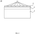
- FIG. 2 a wafer assembly 10 is shown in accordance with an embodiment of the present disclosure.
- FIG. 2 illustrates wafer assembly 10 comprising carrier 1 of FIG. 1 .
- Wafer assembly 10 comprises a wafer, including a plurality of semiconductor dies 11, that is arranged on carrier 1.
- semiconductor dies 11 are arranged on dynamic release layer 4.
- dynamic release layer 4 is configured to be coupled to semiconductor dies 11, and to release one or more of said semiconductor dies 11 when a region of dynamic release layer 4 directly adjacent to said one or more semiconductor dies 11 is illuminated using laser light. Due to secondary support layer 2, the amount of fluence required to release semiconductor dies 11 from dynamic release layer 4 can be relatively low in practice compared to conventional carriers, resulting in a more energy-efficient and cost-effective solution.
- semiconductor dies 11 are arranged on carrier 1 in a row, or in a matrix of rows and columns. Furthermore, semiconductor dies 11 may be mutually spaced apart at fixed, preferably identical distance intervals, though the present disclosure is not limited thereto.
- carrier 1 and wafer assembly 10 are illustrated as planar in FIG. 1 and FIG. 2 , respectively, this need not be the case.
- carrier 1, and consequently also wafer assembly 10 may instead be formed such that wafer assembly 10 is circumferentially arranged along an outer surface of a rotatable drum. The drum can then be rotated to change a position of semiconductor dies 11 relative to an external element, such as a second stage of a pick-and-place apparatus, which apparatus is described in more detail with reference to FIG. 8 .
- carrier 1 in accordance with the present disclosure with reference to FIG. 3-7 .
- each of the embodiments described below similarly relate to a wafer assembly in accordance with the present disclosure comprising said carrier 1 and a wafer including a plurality of semiconductor dies 11, for example as described above.
- carrier 1 is shown in accordance with another embodiment of the present disclosure.
- This embodiment differs from the embodiment in FIG. 1 in that an intermediate layer 5 is provided.
- intermediate layer 5 may for example be an adhesive layer, such as epoxy, acrylic and benzocyclobutene.
- Intermediate layer 5 mutually fixes secondary support layer 2 and primary support layer 3 and can ensure sufficient rigidity and stability of carrier 1.
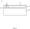
- carrier 1 is shown in accordance with another embodiment of the present disclosure.
- intermediate layer 5 is shown to include a body in which a plurality of recesses 6 are provided. These recesses or cavities 6 may hold or be filled with a gaseous medium and/or a third material different from the first material.
- the third material may include aerogel.
- cavities are equally envisaged. That is, instead of (or in addition to) recesses in an outer surface of the body, said body could comprise one or more cavities which the body surrounds. The cavities may then hold or be filled with the third material or a gaseous medium as explained above.
- carrier 1 is shown in accordance with another embodiment of the present disclosure.
- intermediate layer 5, not including cavities or recesses 6, may be made of the first material, and may be preferably integrally connected to primary support layer 3 as shown in FIG. 5 .
- intermediate layer 5 can be easily manufactured by forming a plurality of cavities or recesses 6 at a side of primary support layer 3, and optionally at least partially filling them with the third material or a gaseous medium.
- cavities are equally envisaged instead of or in addition to recesses 6. That is, instead of (or in addition to) recesses in an outer surface of the body, said body could comprise one or more cavities which the body surrounds. The cavities may then hold or be filled with the third material or a gaseous medium as explained above.
- recesses 6 may be formed to further prevent or at least mitigate thermal energy from flowing away from dynamic release layer 4.
- primary support layer 3 is illustrated as being formed entirely by a single region of the first material. However, the present disclosure is not limited thereto. Rather, primary support layer 3 may include more than one region of an optically transparent first material, and may optionally further include regions of a different material, as discussed below in more detail with reference to FIG. 6 .
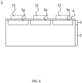
- carrier 1 is shown in accordance with another embodiment of the present disclosure.
- primary support layer 3 comprises a plurality of mutually separated regions 3a of first material arranged in a body of second material.
- said body of second material may be integrally formed with secondary support layer 2.
- Secondary support layer 2 and primary support layer 3 could then be manufactured by first providing a main body of second material, forming a plurality of recesses, and filling said recesses with first material to form regions 3a. Nevertheless, the present disclosure is not limited thereto.
- the wafer including semiconductor dies 11 can be arranged on carrier 1 such that semiconductor dies 11 are attached to dynamic release layer 4 adjacent to regions 3a of primary support layer 3. This allows preventing or at least mitigating heat flow away from dynamic release layer 4 without compromising the interface between dynamic release layer 4 and primary support layer 3 at positions where semiconductor dies 11 are configured to be arranged.
- dynamic release layer 4 is formed as a single contiguous layer that covers primary support layer 3.
- dynamic release layer 4 may cover primary support layer 3 entirely.
- present disclosure is not limited thereto.
- carrier 1 is shown in accordance with another embodiment of the present disclosure, which differs from the embodiment in FIG. 6 in that dynamic release layer 4 comprises a plurality of mutually separated regions 4a, each being arranged adjacent to a respective region 3a of primary support layer 3.
- the wafer may for example be arranged on carrier 1 such that semiconductor dies 11 are attached to regions 4a of dynamic release layer 4 directly adjacent to regions 3a of primary support layer 3.
- dynamic release layer 4a may be patterned before, during, or after being arranged on primary support layer 3.
- FIG. 7 allows preventing or at least mitigating heat flow away from dynamic release layer 4 without compromising the interface between dynamic release layer 4 and primary support layer 3 at positions where semiconductor dies 11 are configured to be arranged.
- the amount of material required for dynamic release layer 4 can be reduced.
- regions 4a of dynamic release layer 4 can also be used for accurate positioning of semiconductor dies 11 to form wafer assembly 10.
- dynamic release layer 4 as a plurality of regions 4a is described with reference to FIG. 7 , this concept may be identically or similarly applied to any of the embodiments described with reference to FIG. 1-6 .
- second stage 22 may represent a next stage on which the semiconductor die 11 is to be carried or processed further.
- second stage 22 is shown to include a substrate 24 and a receiving element 25 configured to receive semiconductor die 11.
- substrate 24 may for example be a printed circuit board (PCB) on which semiconductor die 11 is to be mounted via receiving elements 25 (e.g., solder bumps).
- PCB printed circuit board
- receiving elements 25 e.g., solder bumps
- second stage 22 is configured to receive semiconductor die 11a from first stage 21 when carrier 1 is illuminated using laser source 23.
- laser source 23 illuminates dynamic release layer 4 directly adjacent to semiconductor die 11a to activate the release function of dynamic release layer 4 and release semiconductor die 11 from first stage 21 to propagate it to second stage 22, as illustrated in FIG. 8 using arrows to indicate the direction of propagation of semiconductor die 11a. Since dynamic release layer 4 is only illuminated locally to release semiconductor die 11a specifically, remaining semiconductor dies 11 of the wafer can remain coupled to dynamic release layer 4.
Landscapes
- Container, Conveyance, Adherence, Positioning, Of Wafer (AREA)
Abstract
Description
- The present disclosure generally relates to a carrier for laser die transfer of semiconductor dies. The present disclosure further relates to a wafer assembly comprising such a carrier, and a pick-and-place apparatus comprising such a carrier.
- Carriers for laser die transfer of semiconductor dies, typically for use in a pick-and-place apparatus, are known in the art. In such an apparatus, a wafer comprising a plurality of semiconductor dies is provided on a carrier. The carrier includes a primary support layer for supporting the wafer. In conventional laser die transfer applications, the primary support layer is optically transparent, and the wafer is arranged on a dynamic release layer attached to the primary support layer. The dynamic release layer is configured to release one or more semiconductor dies among said plurality of said semiconductor dies when a region of the dynamic release layer directly adjacent to said one or more semiconductor dies is illuminated using a laser. In this manner, said one or more semiconductor dies can be released from a carrier to transfer them to a second stage of the pick-and-place apparatus at a predetermined position for further processing of the semiconductor dies.
- For the dynamic release layer to release the semiconductor dies, sufficient energy must be provided thereto via the laser. A measure for the required energy may typically be expressed as `fluence', or the energy of the laser pulse divided by the area it is illuminating.
- At least for the purpose of energy efficiency as well as cost-effectiveness, there is a need for improving (i.e., reducing) the fluence required for releasing the semiconductor dies from the dynamic release layer.
- It is an object of the present disclosure to provide a carrier for laser die transfer in which the abovementioned problems do not occur, or hardly so.
- According to an aspect of the present disclosure, a carrier for laser die transfer of semiconductor dies is provided. The carrier comprises an optically transparent secondary support layer, an optically transparent primary support layer attached to the secondary support layer, said primary support layer comprising one or more regions of an optically transparent first material, and a dynamic release layer attached to the primary support layer, wherein the dynamic release layer contacts the one or more regions of a first material. The dynamic release layer is configured to be coupled to a plurality of semiconductor dies, and to release one or more semiconductor dies among said plurality of said semiconductor dies when a region of the dynamic release layer directly adjacent to said one or more semiconductor dies is illuminated using laser light. The secondary support layer has a material composition different from the first material for reducing a flow of heat away from the primary support layer during the laser die transfer process.
- The Applicant has found that conventional carriers for laser die transfer applications may have an associated disadvantage that the primary support layer may absorb heat and effectively act as a heatsink. When a laser is applied to the carrier, part of the energy that should have been absorbed by the dynamic release layer will instead flow into the primary support layer and away from the dynamic release layer. As a result, the fluence required to release the semiconductor die from the carrier may be significantly higher than the energy that is actually absorbed by the dynamic release layer.
- In accordance with the present disclosure, the secondary support layer, having a different material composition compared to the primary support layer, is provided to prevent or at least mitigate a flow of heat away from the primary support layer during the laser die transfer process. The Applicant has found that, compared to conventional carriers which may use glass primary support layers, the use of a secondary support layer in accordance with the present disclosure can provide a more than ten times reduction in fluence required to activate the release process.
- Moreover, in accordance with the present disclosure, key properties of the primary support layer can be maintained with the arrangement described above. For example, the structure can remain chemically similar to conventional 'glass' carriers, and the interface between the primary support layer and the dynamic release layer can still withstand sufficient temperature as is the case in conventional carriers.
- The thermal diffusivity of the material composition can be at least 2 times smaller than the thermal diffusivity of the first material, preferably at least 5 times smaller, and more preferably at least 10 times smaller.
- The secondary support layer may comprise a substrate layer. The substrate layer may be made from a second material different from the first material.
- The carrier may further comprise an intermediate layer. The substrate layer may be connected to the primary support layer through the intermediate layer.
- In a further embodiment, the intermediate layer may comprise an adhesive layer.
- Alternatively, the intermediate layer may comprise a body made from the second material, said body comprising a plurality of cavities or recesses that either hold a gaseous medium or are filed with a third material different from the first material. For example, the body may be integrally connected to the substrate layer.
- Alternatively, the intermediate layer may comprise a body made from the first material, said body comprising a plurality of cavities or recesses that hold a gaseous medium and/or are filed with a third material different from the first material. For example, the body may be integrally connected to the primary support layer.
- The cavities or recesses can further aid in preventing or at least mitigating heat flow away from the dynamic release layer, thus reducing the fluence required for releasing the dies.
- The primary support layer may be formed entirely by a single region of the first material.
- Alternatively, the one or more regions of the primary support layer may comprise mutually separated regions of the first material that are arranged in a body of a material different from the first material, such as the second material. As a result, a thermal barrier can effectively be provided not only below the primary support layer but also adjacent to the primary support layer with respect to the dynamic release layer. In these cases, semiconductor dies may be configured to be provided on the dynamic release layer where said dynamic release layer is in contact with the mutually separated regions to allow sufficient heat resistance of the interface between the dynamic release layer and the primary support layer where this is required, and provide a thermal barrier functionality to the primary support layer in a remainder thereof, thereby both minimizing the use of the first material and the fluence required to release the semiconductor dies from the dynamic release layer in practice.
- The dynamic release layer may comprise a contiguous layer that covers the one or more regions of the primary support layer. Such a configuration is easily manufacturable as the dynamic release layer pattern need not be positioned accurately. For example, the dynamic release layer may cover the primary support layer entirely.
- The dynamic release layer may comprises a plurality of mutually separated regions, each region of the dynamic release layer directly contacting a respective region of the primary support layer. As a result, the amount of material required to form the dynamic release layer can be minimized, for example by only arranging the dynamic release layer in so far as required for attaching the semiconductor die thereto.
- In the above, various components and layers of the carrier have been described in accordance with the present disclosure. These components and layers may have the following exemplary thicknesses and/or materials, though the present disclosure is not limited thereto.
- The primary support layer may have a thickness in a range between 0.01 and 1 mm. Additionally or alternatively, the secondary support layer may have a thickness in a range between 0.01 and 0.1 mm. Additionally or alternatively, the dynamic release layer may have a thickness in a range between 1 and 100 µm. Additionally or alternatively, the body of the secondary support layer may have a thickness in a range between 0.01 and 0.1 mm. Additionally or alternatively, the mutually separated regions of the first material may have a thickness in a range between 0.01 and 0.1 mm.
- The first material may comprise at least one of glass, e.g., quartz glass, BK7 (which is a type of borosilicate glass), or the like, ceramic or siloxane. Additionally or alternatively, the second material may comprise at least one of polyethylene terephthalate (PET), polyethylene naphthalate (PEN), polyimide (PI) and polyvinyl chloride (PVC). Additionally or alternatively, the dynamic release layer may be made of at least one of molybdenum, aluminum, tin and indium. Additionally or alternatively, the adhesive layer may be made of at least one of epoxy, acrylic and benzocyclobutene. Additionally or alternatively, the third material may comprise at least one of aerogel and siloxane.
- According to another aspect of the present disclosure, a wafer assembly is provided. The wafer assembly comprises the carrier according to any of the embodiments described above, and a wafer comprising a plurality of mutually separated semiconductor dies. The wafer is arranged on the carrier.
- According to yet another aspect of the present disclosure, a pick-and-place apparatus is provided. The apparatus comprises a first stage comprising a carrier according to any of the embodiments described above, a laser source for illuminating the carrier, and a second stage configured to receive one or more semiconductor dies from the first stage when the carrier is illuminated using the laser source.
- So that the manner in which the features of the present disclosure can be understood in detail, a more particular description is made with reference to embodiments, some of which are illustrated in the appended figures. It is to be noted, however, that the appended figures illustrate only typical embodiments and are therefore not to be considered limiting of its scope. The figures are for facilitating an understanding of the disclosure and thus are not necessarily drawn to scale. Advantages of the subject matter claimed will become apparent to those skilled in the art upon reading this description in conjunction with the accompanying figures, in which like reference numerals have been used to designate like elements, and in which:
-
FIG. 1 is a cross-sectional view of a carrier in accordance with an embodiment of the present disclosure; -
FIG. 2 is a cross-sectional view of a wafer assembly in accordance with an embodiment of the present disclosure; -
FIG. 3 is a cross-sectional view of a carrier in accordance with an embodiment of the present disclosure; -
FIG. 4 is a cross-sectional view of a carrier in accordance with an embodiment of the present disclosure; -
FIG. 5 is a cross-sectional view of a carrier in accordance with an embodiment of the present disclosure; -
FIG. 6 is a cross-sectional view of a carrier in accordance with an embodiment of the present disclosure; -
FIG. 7 is a schematic diagram of a pick-and-place apparatus in accordance with an embodiment of the present disclosure; and -
FIG. 8 is a schematic diagram of a pick-and-place apparatus in accordance with an embodiment of the present disclosure. - The present disclosure is described in conjunction with the appended figures. It is emphasized that, in accordance with the standard practice in the industry, various features are not drawn to scale. In fact, the dimensions of the various features may be arbitrarily increased or reduced for clarity of discussion.
- In the appended figures, similar components and/or features may have the same reference label. Further, various components of the same type may be distinguished by following the reference label by a dash and a second label that distinguishes among the similar components. If only the first reference label is used in the specification, the description is applicable to any one of the similar components having the same first reference label irrespective of the second reference label.
- Unless the context clearly requires otherwise, throughout the description and the claims, the words "comprise," "comprising," and the like are to be construed in an inclusive sense, as opposed to an exclusive or exhaustive sense; that is to say, in the sense of "including, but not limited to." As used herein, the terms "connected," "coupled," or any variant thereof means any connection or coupling, either direct or indirect, between two or more elements; the coupling or connection between the elements can be physical, logical, electromagnetic, or a combination thereof. Additionally, the words "herein," "above," "below," and words of similar import, when used in this application, refer to this application as a whole and not to any particular portions of this application. Where the context permits, words in the detailed description using the singular or plural number may also include the plural or singular number respectively. The word "or," in reference to a list of two or more items, covers all of the following interpretations of the word: any of the items in the list, all of the items in the list, and any combination of the items in the list.
- The teachings of the technology provided herein can be applied to other systems, not necessarily the system described below. The elements and acts of the various examples described below can be combined to provide further implementations of the technology. Some alternative implementations of the technology may include not only additional elements to those implementations noted below, but also may include fewer elements.
- These and other changes can be made to the technology in light of the following detailed description. While the description describes certain examples of the technology, and describes the best mode contemplated, no matter how detailed the description appears, the technology can be practiced in many ways. Details of the system may vary considerably in its specific implementation, while still being encompassed by the technology disclosed herein. As noted above, particular terminology used when describing certain features or aspects of the technology should not be taken to imply that the terminology is being redefined herein to be restricted to any specific characteristics, features, or aspects of the technology with which that terminology is associated. In general, the terms used in the following claims should not be construed to limit the technology to the specific examples disclosed in the specification, unless the detailed description section explicitly defines such terms. Accordingly, the actual scope of the technology encompasses not only the disclosed examples, but also all equivalent ways of practicing or implementing the technology under the claims.
- To reduce the number of claims, certain aspects of the technology are presented below in certain claim forms, but the applicant contemplates the various aspects of the technology in any number of claim forms.
- In
FIG. 1 , acarrier 1 in accordance with an embodiment of the present disclosure is shown. Here,carrier 1 comprises asecondary support layer 2, aprimary support layer 3, and adynamic release layer 4.Primary support layer 3 includes one or more regions of an optically transparent first material, such as glass, e.g., quartz glass or BK7. In this embodiment,primary support layer 3 is made entirely from said optically transparent first material. -
Secondary support layer 2 is also optically transparent, but is made from a different material or material composition that provides the functionality of reducing a flow of heat away from the primary support layer during the laser die transfer process. For example,secondary support layer 2 includes a substrate layer made of a second material different from the first material. The second material may for example include PET, PEN, or the like. - In
FIG. 2 , awafer assembly 10 is shown in accordance with an embodiment of the present disclosure. In particular,FIG. 2 illustrateswafer assembly 10 comprisingcarrier 1 ofFIG. 1 . -
Wafer assembly 10 comprises a wafer, including a plurality of semiconductor dies 11, that is arranged oncarrier 1. In particular, semiconductor dies 11 are arranged ondynamic release layer 4. Here,dynamic release layer 4 is configured to be coupled to semiconductor dies 11, and to release one or more of said semiconductor dies 11 when a region ofdynamic release layer 4 directly adjacent to said one or more semiconductor dies 11 is illuminated using laser light. Due tosecondary support layer 2, the amount of fluence required to release semiconductor dies 11 fromdynamic release layer 4 can be relatively low in practice compared to conventional carriers, resulting in a more energy-efficient and cost-effective solution. - In an example, semiconductor dies 11 are arranged on
carrier 1 in a row, or in a matrix of rows and columns. Furthermore, semiconductor dies 11 may be mutually spaced apart at fixed, preferably identical distance intervals, though the present disclosure is not limited thereto. - Although
carrier 1 andwafer assembly 10 are illustrated as planar inFIG. 1 andFIG. 2 , respectively, this need not be the case. As will be appreciated by the skilled person,carrier 1, and consequently alsowafer assembly 10, may instead be formed such thatwafer assembly 10 is circumferentially arranged along an outer surface of a rotatable drum. The drum can then be rotated to change a position of semiconductor dies 11 relative to an external element, such as a second stage of a pick-and-place apparatus, which apparatus is described in more detail with reference toFIG. 8 . - In the ensuing description below, reference will be made to
carrier 1 in accordance with the present disclosure with reference toFIG. 3-7 . As will be appreciated by the skilled person, each of the embodiments described below similarly relate to a wafer assembly in accordance with the present disclosure comprising saidcarrier 1 and a wafer including a plurality of semiconductor dies 11, for example as described above. - In
FIG. 3 ,carrier 1 is shown in accordance with another embodiment of the present disclosure. This embodiment differs from the embodiment inFIG. 1 in that anintermediate layer 5 is provided. In this case,intermediate layer 5 may for example be an adhesive layer, such as epoxy, acrylic and benzocyclobutene.Intermediate layer 5 mutually fixessecondary support layer 2 andprimary support layer 3 and can ensure sufficient rigidity and stability ofcarrier 1. - In
FIG. 4 ,carrier 1 is shown in accordance with another embodiment of the present disclosure. Here,intermediate layer 5 is shown to include a body in which a plurality of recesses 6 are provided. These recesses or cavities 6 may hold or be filled with a gaseous medium and/or a third material different from the first material. For example, the third material may include aerogel. - The body of
intermediate layer 5 may be made of the second material in this embodiment. In a preferred embodiment,intermediate layer 5 is integrally connected tosecondary support layer 2, in which case the remainder ofintermediate layer 5 not including recesses or cavities 6 is made of the second material. In the latter case,intermediate layer 5 can be easily manufactured by forming a plurality of cavities or recesses 6 at a side ofsecondary support layer 2, and optionally at least partially filling them with the third material or a gaseous medium. For example, the gaseous medium may include air or a vacuum. - Instead of recesses 6, cavities are equally envisaged. That is, instead of (or in addition to) recesses in an outer surface of the body, said body could comprise one or more cavities which the body surrounds. The cavities may then hold or be filled with the third material or a gaseous medium as explained above.
- In
FIG. 5 ,carrier 1 is shown in accordance with another embodiment of the present disclosure. Here,intermediate layer 5, not including cavities or recesses 6, may be made of the first material, and may be preferably integrally connected toprimary support layer 3 as shown inFIG. 5 . In the latter case,intermediate layer 5 can be easily manufactured by forming a plurality of cavities or recesses 6 at a side ofprimary support layer 3, and optionally at least partially filling them with the third material or a gaseous medium. - In the embodiment shown in
FIG. 5 , similarly toFIG. 4 , cavities are equally envisaged instead of or in addition to recesses 6. That is, instead of (or in addition to) recesses in an outer surface of the body, said body could comprise one or more cavities which the body surrounds. The cavities may then hold or be filled with the third material or a gaseous medium as explained above. - In the embodiments shown in
FIG. 4 andFIG. 5 , recesses 6 (and/or cavities) may be formed to further prevent or at least mitigate thermal energy from flowing away fromdynamic release layer 4. - In the embodiments shown in
FIG. 1-5 ,primary support layer 3 is illustrated as being formed entirely by a single region of the first material. However, the present disclosure is not limited thereto. Rather,primary support layer 3 may include more than one region of an optically transparent first material, and may optionally further include regions of a different material, as discussed below in more detail with reference toFIG. 6 . - In
FIG. 6 ,carrier 1 is shown in accordance with another embodiment of the present disclosure. Here,primary support layer 3 comprises a plurality of mutually separated regions 3a of first material arranged in a body of second material. In a preferred embodiment, said body of second material may be integrally formed withsecondary support layer 2.Secondary support layer 2 andprimary support layer 3 could then be manufactured by first providing a main body of second material, forming a plurality of recesses, and filling said recesses with first material to form regions 3a. Nevertheless, the present disclosure is not limited thereto. - As shown in
FIG. 6 , the wafer including semiconductor dies 11 can be arranged oncarrier 1 such that semiconductor dies 11 are attached todynamic release layer 4 adjacent to regions 3a ofprimary support layer 3. This allows preventing or at least mitigating heat flow away fromdynamic release layer 4 without compromising the interface betweendynamic release layer 4 andprimary support layer 3 at positions where semiconductor dies 11 are configured to be arranged. - As will be appreciated by the skilled person, forming
primary support layer 3 using one or more mutually separated regions 3a of the first material could be equally applied to any of the embodiments described with reference toFIG. 1-5 . - In the above, embodiments are shown wherein
dynamic release layer 4 is formed as a single contiguous layer that coversprimary support layer 3. For example,dynamic release layer 4 may coverprimary support layer 3 entirely. However, the present disclosure is not limited thereto. - To illustrate this, in
FIG. 7 ,carrier 1 is shown in accordance with another embodiment of the present disclosure, which differs from the embodiment inFIG. 6 in thatdynamic release layer 4 comprises a plurality of mutually separated regions 4a, each being arranged adjacent to a respective region 3a ofprimary support layer 3. The wafer may for example be arranged oncarrier 1 such that semiconductor dies 11 are attached to regions 4a ofdynamic release layer 4 directly adjacent to regions 3a ofprimary support layer 3. In an example, dynamic release layer 4a may be patterned before, during, or after being arranged onprimary support layer 3. - Similarly to
FIG. 6 , the embodiment ofFIG. 7 allows preventing or at least mitigating heat flow away fromdynamic release layer 4 without compromising the interface betweendynamic release layer 4 andprimary support layer 3 at positions where semiconductor dies 11 are configured to be arranged. In addition, the amount of material required fordynamic release layer 4 can be reduced. Moreover, regions 4a ofdynamic release layer 4 can also be used for accurate positioning of semiconductor dies 11 to formwafer assembly 10. - As will be appreciated by the skilled person, although forming
dynamic release layer 4 as a plurality of regions 4a is described with reference toFIG. 7 , this concept may be identically or similarly applied to any of the embodiments described with reference toFIG. 1-6 . - In
FIG. 8 , a pick-and-place apparatus 20 is shown in accordance with an embodiment of the present disclosure. Pick-and-place apparatus 20 comprises afirst stage 21, formed by or including a wafer assembly (e.g.,wafer assembly 10 ofFIG. 2 ), asecond stage 22, and alaser source 23. - Here,
second stage 22 may represent a next stage on which the semiconductor die 11 is to be carried or processed further. For example,second stage 22 is shown to include asubstrate 24 and a receivingelement 25 configured to receive semiconductor die 11. This may already be an end stage of the process, i.e.,substrate 24 may for example be a printed circuit board (PCB) on which semiconductor die 11 is to be mounted via receiving elements 25 (e.g., solder bumps). However, the present disclosure is not limited thereto. - In pick-and-
place apparatus 20,second stage 22 is configured to receive semiconductor die 11a fromfirst stage 21 whencarrier 1 is illuminated usinglaser source 23. In particular,laser source 23 illuminatesdynamic release layer 4 directly adjacent to semiconductor die 11a to activate the release function ofdynamic release layer 4 and release semiconductor die 11 fromfirst stage 21 to propagate it tosecond stage 22, as illustrated inFIG. 8 using arrows to indicate the direction of propagation of semiconductor die 11a. Sincedynamic release layer 4 is only illuminated locally to release semiconductor die 11a specifically, remaining semiconductor dies 11 of the wafer can remain coupled todynamic release layer 4. - The ensuing description above provides preferred exemplary embodiment(s) only, and is not intended to limit the scope, applicability, or configuration of the disclosure. Rather, the ensuing description of the preferred exemplary embodiment(s) will provide those skilled in the art with an enabling description for implementing a preferred exemplary embodiment of the disclosure, it being understood that various changes may be made in the function and arrangement of elements, including various modifications and/or combinations of features from different embodiments, without departing from the scope of the present disclosure as defined by the appended claims and, at least in some jurisdictions, their equivalents.
Claims (15)
- A carrier for laser die transfer of semiconductor dies, comprising:an optically transparent secondary support layer;an optically transparent primary support layer attached to the secondary support layer, said primary support layer comprising one or more regions of an optically transparent first material; anda dynamic release layer attached to the primary support layer, wherein the dynamic release layer contacts the one or more regions of a first material, the dynamic release layer being configured to be coupled to a plurality of semiconductor dies, and to release one or more semiconductor dies among said plurality of said semiconductor dies when a region of the dynamic release layer directly adjacent to said one or more semiconductor dies is illuminated using laser light,wherein the secondary support layer has a material composition different from the first material for reducing a flow of heat away from the primary support layer during the laser die transfer process.
- The carrier according to claim 1, wherein the thermal diffusivity of the material composition is at least 2 times smaller than the thermal diffusivity of the first material, preferably at least 5 times smaller, and more preferably at least 10 times smaller.
- The carrier according to claim 1 or 2, wherein the secondary support layer comprises a substrate layer, wherein the substrate layer is made from a second material different from the first material.
- The carrier according to claim 3, wherein the carrier further comprises an intermediate layer, wherein the substrate layer is connected to the primary support layer through the intermediate layer.
- The carrier according to claim 4, wherein the intermediate layer comprises an adhesive layer.
- The carrier according to claim 4, wherein the intermediate layer comprises a body made from the second material, said body comprising a plurality of cavities or recesses that either hold a gaseous medium or are filed with a third material different from the first material.
- The carrier according to claim 6, wherein the body is integrally connected to the substrate layer.
- The carrier according to claim 4, wherein the intermediate layer comprises a body made from the first material, said body comprising a plurality of cavities or recesses that hold a gaseous medium and/or are filed with a third material different from the first material, wherein the body is preferably integrally connected to the primary support layer.
- The carrier according to any of the previous claims, wherein the primary support layer is formed entirely by a single region of the first material.
- The carrier according to any of the claims 1-8, wherein the one or more regions of the primary support layer comprises mutually separated regions of the first material that are arranged in a body of the second material different from the first material.
- The carrier according to any of the previous claims, wherein the dynamic release layer comprises a contiguous layer that covers the one or more regions of the primary support layer, wherein the dynamic release layer preferably covers the primary support layer entirely, or
wherein the dynamic release layer comprises a plurality of mutually separated regions, each region of the dynamic release layer directly contacting a respective region of the primary support layer. - The carrier according to any of the previous claims, wherein:the primary support layer has a thickness in a range between 0.01 and 1.0 mm; and/orthe secondary support layer has a thickness in a range between 0.01 and 0.1 mm; and/orthe dynamic release layer has a thickness in a range between 1 and 100 micrometer; and/orin so far as depending on any of the claims 6-8, the body of the secondary support layer has a thickness in a range between 0.01 and 0.1 mm; and/orin so far as depending on claim 10, wherein the mutually separated regions of the first material have a thickness in a range between 0.01 and 0.1 mm.
- The carrier according to any of the previous claims, wherein:the first material comprises at least one of glass, such as BK7 or quartz, ceramic and siloxane;
and/orthe second material comprises at least one of polyethylene terephthalate, PET, polyethylene naphthalate, PEN, polyimide, PI, and polyvinylchloride, PVC; and/orthe dynamic release layer comprises at least one of molybdenum, aluminum, tin, and indium; and/orin so far as depending on claim 5, the adhesive layer comprises at least one of epoxy, acrylic and benzocyclobutene; and/orin so far as depending on claim 6 or 8, the third material comprises at least one of aerogel and siloxane. - A wafer assembly, comprising:The carrier according to any of the previous claims;a wafer comprising a plurality of mutually separated semiconductor dies, wherein the wafer is arranged on the carrier.
- A pick-and-place apparatus, comprising:a first stage comprising a wafer assembly according to claim 14;a laser source for illuminating the carrier; anda second stage configured to receive one or more semiconductor dies from the first stage when the carrier is illuminated using the laser source.
Priority Applications (2)
| Application Number | Priority Date | Filing Date | Title |
|---|---|---|---|
| EP23201054.6A EP4531080A1 (en) | 2023-09-29 | 2023-09-29 | Carrier for laser die transfer, wafer assembly, and pick and place apparatus comprising the same |
| PCT/EP2024/077389 WO2025068583A1 (en) | 2023-09-29 | 2024-09-27 | Carrier for laser die transfer, wafer assembly, and pick and place apparatus comprising the same |
Applications Claiming Priority (1)
| Application Number | Priority Date | Filing Date | Title |
|---|---|---|---|
| EP23201054.6A EP4531080A1 (en) | 2023-09-29 | 2023-09-29 | Carrier for laser die transfer, wafer assembly, and pick and place apparatus comprising the same |
Publications (1)
| Publication Number | Publication Date |
|---|---|
| EP4531080A1 true EP4531080A1 (en) | 2025-04-02 |
Family
ID=88238015
Family Applications (1)
| Application Number | Title | Priority Date | Filing Date |
|---|---|---|---|
| EP23201054.6A Pending EP4531080A1 (en) | 2023-09-29 | 2023-09-29 | Carrier for laser die transfer, wafer assembly, and pick and place apparatus comprising the same |
Country Status (2)
| Country | Link |
|---|---|
| EP (1) | EP4531080A1 (en) |
| WO (1) | WO2025068583A1 (en) |
Citations (5)
| Publication number | Priority date | Publication date | Assignee | Title |
|---|---|---|---|---|
| US20210053297A1 (en) * | 2019-08-23 | 2021-02-25 | SelfArray, Inc. | Methods and systems for controlling temperature across a region defined by using thermally conductive elements |
| US20210375659A1 (en) * | 2019-02-15 | 2021-12-02 | Kulicke & Soffa Netherlands B.V. | Dynamic release tapes for assembly of discrete components |
| US20220093423A1 (en) * | 2020-09-22 | 2022-03-24 | Kulicke & Soffa Netherlands B.V. | Reusable die catch materials, reusable die release materials, related die transfer systems, and methods of using the same |
| US20230017084A1 (en) * | 2019-12-17 | 2023-01-19 | Kulicke & Soffa Netherlands B.V. | Adhesive tapes for receiving discrete components |
| US20230107245A1 (en) * | 2021-10-01 | 2023-04-06 | Kulicke & Soffa Netherlands B.V. | Methods of transferring a die from a carrier to a receive substrate, and related systems and materials |
Family Cites Families (1)
| Publication number | Priority date | Publication date | Assignee | Title |
|---|---|---|---|---|
| DE102022102364A1 (en) * | 2022-02-01 | 2023-08-03 | OSRAM Opto Semiconductors Gesellschaft mit beschränkter Haftung | DEVICE FOR TRANSFER AND METHOD |
-
2023
- 2023-09-29 EP EP23201054.6A patent/EP4531080A1/en active Pending
-
2024
- 2024-09-27 WO PCT/EP2024/077389 patent/WO2025068583A1/en active Pending
Patent Citations (5)
| Publication number | Priority date | Publication date | Assignee | Title |
|---|---|---|---|---|
| US20210375659A1 (en) * | 2019-02-15 | 2021-12-02 | Kulicke & Soffa Netherlands B.V. | Dynamic release tapes for assembly of discrete components |
| US20210053297A1 (en) * | 2019-08-23 | 2021-02-25 | SelfArray, Inc. | Methods and systems for controlling temperature across a region defined by using thermally conductive elements |
| US20230017084A1 (en) * | 2019-12-17 | 2023-01-19 | Kulicke & Soffa Netherlands B.V. | Adhesive tapes for receiving discrete components |
| US20220093423A1 (en) * | 2020-09-22 | 2022-03-24 | Kulicke & Soffa Netherlands B.V. | Reusable die catch materials, reusable die release materials, related die transfer systems, and methods of using the same |
| US20230107245A1 (en) * | 2021-10-01 | 2023-04-06 | Kulicke & Soffa Netherlands B.V. | Methods of transferring a die from a carrier to a receive substrate, and related systems and materials |
Also Published As
| Publication number | Publication date |
|---|---|
| WO2025068583A1 (en) | 2025-04-03 |
Similar Documents
| Publication | Publication Date | Title |
|---|---|---|
| TWI233701B (en) | Light-source module and its production method | |
| US7701726B2 (en) | Method of manufacturing a wiring substrate and semiconductor device | |
| EP1498013B1 (en) | Flexible interconnect structures for electrical devices and light sources incorporating the same | |
| US6700136B2 (en) | Light emitting device package | |
| KR102552894B1 (en) | Electronic package containing multi-layer stiffeners | |
| KR20190087631A (en) | Flexible display screen and flexible display device | |
| CN114507488A (en) | Conductive film, wound body, connection structure, and method for producing connection structure | |
| KR20150067302A (en) | Embedding thin chips in polymer | |
| EP2445024B1 (en) | Led array module and fabrication method thereof | |
| US8860042B2 (en) | Light module having metal clamps | |
| CN115110027B (en) | Evaporation mask and manufacturing method thereof | |
| JP3687204B2 (en) | Multilayer wiring pattern forming method | |
| WO2025068583A1 (en) | Carrier for laser die transfer, wafer assembly, and pick and place apparatus comprising the same | |
| KR100944274B1 (en) | Flexible circuit board and method for fabricating the board, semiconductor package comprising the board and method for fabricating the package | |
| WO2017038171A1 (en) | Optical member and optical irradiation device | |
| US12119363B2 (en) | Sensor package structure | |
| CN111165078B (en) | Wired circuit board | |
| US20240306294A1 (en) | Circuit device | |
| US12369246B2 (en) | Side wiring structure and manufacturing method thereof | |
| JP3564560B2 (en) | Flexible thin plate heat pipe | |
| CN117913149A (en) | Sensor packaging structure and manufacturing method thereof | |
| US20230403826A1 (en) | Heat dissipation substrate | |
| CN107170713B (en) | Substrate and multi-substrate including a plurality of the substrates and method for manufacturing the same | |
| CN111565508B (en) | PCB structure for verifying heat resistance of different materials | |
| US20230395452A1 (en) | Electronic device and manufacturing method thereof |
Legal Events
| Date | Code | Title | Description |
|---|---|---|---|
| PUAI | Public reference made under article 153(3) epc to a published international application that has entered the european phase |
Free format text: ORIGINAL CODE: 0009012 |
|
| STAA | Information on the status of an ep patent application or granted ep patent |
Free format text: STATUS: THE APPLICATION HAS BEEN PUBLISHED |
|
| AK | Designated contracting states |
Kind code of ref document: A1 Designated state(s): AL AT BE BG CH CY CZ DE DK EE ES FI FR GB GR HR HU IE IS IT LI LT LU LV MC ME MK MT NL NO PL PT RO RS SE SI SK SM TR |
|
| STAA | Information on the status of an ep patent application or granted ep patent |
Free format text: STATUS: REQUEST FOR EXAMINATION WAS MADE |
|
| 17P | Request for examination filed |
Effective date: 20251002 |
|
| RIN1 | Information on inventor provided before grant (corrected) |
Inventor name: STOKKERMANS, JOZEF PETRUS WILHELMUS Inventor name: WESSELINGH, JASPER |