EP4529070A1 - Radio frequency front end device, antenna module, and electronic device - Google Patents
Radio frequency front end device, antenna module, and electronic device Download PDFInfo
- Publication number
- EP4529070A1 EP4529070A1 EP23908957.6A EP23908957A EP4529070A1 EP 4529070 A1 EP4529070 A1 EP 4529070A1 EP 23908957 A EP23908957 A EP 23908957A EP 4529070 A1 EP4529070 A1 EP 4529070A1
- Authority
- EP
- European Patent Office
- Prior art keywords
- radio frequency
- switch
- filter
- matching circuit
- end device
- Prior art date
- Legal status (The legal status is an assumption and is not a legal conclusion. Google has not performed a legal analysis and makes no representation as to the accuracy of the status listed.)
- Pending
Links
Images




Classifications
-
- H—ELECTRICITY
- H04—ELECTRIC COMMUNICATION TECHNIQUE
- H04B—TRANSMISSION
- H04B1/00—Details of transmission systems, not covered by a single one of groups H04B3/00 - H04B13/00; Details of transmission systems not characterised by the medium used for transmission
- H04B1/06—Receivers
- H04B1/16—Circuits
- H04B1/18—Input circuits, e.g. for coupling to an antenna or a transmission line
-
- H—ELECTRICITY
- H03—ELECTRONIC CIRCUITRY
- H03H—IMPEDANCE NETWORKS, e.g. RESONANT CIRCUITS; RESONATORS
- H03H1/00—Constructional details of impedance networks whose electrical mode of operation is not specified or applicable to more than one type of network
- H03H1/0007—Constructional details of impedance networks whose electrical mode of operation is not specified or applicable to more than one type of network of radio frequency interference filters
-
- H—ELECTRICITY
- H04—ELECTRIC COMMUNICATION TECHNIQUE
- H04B—TRANSMISSION
- H04B1/00—Details of transmission systems, not covered by a single one of groups H04B3/00 - H04B13/00; Details of transmission systems not characterised by the medium used for transmission
- H04B1/005—Details of transmission systems, not covered by a single one of groups H04B3/00 - H04B13/00; Details of transmission systems not characterised by the medium used for transmission adapting radio receivers, transmitters andtransceivers for operation on two or more bands, i.e. frequency ranges
- H04B1/0053—Details of transmission systems, not covered by a single one of groups H04B3/00 - H04B13/00; Details of transmission systems not characterised by the medium used for transmission adapting radio receivers, transmitters andtransceivers for operation on two or more bands, i.e. frequency ranges with common antenna for more than one band
- H04B1/006—Details of transmission systems, not covered by a single one of groups H04B3/00 - H04B13/00; Details of transmission systems not characterised by the medium used for transmission adapting radio receivers, transmitters andtransceivers for operation on two or more bands, i.e. frequency ranges with common antenna for more than one band using switches for selecting the desired band
-
- H—ELECTRICITY
- H04—ELECTRIC COMMUNICATION TECHNIQUE
- H04B—TRANSMISSION
- H04B1/00—Details of transmission systems, not covered by a single one of groups H04B3/00 - H04B13/00; Details of transmission systems not characterised by the medium used for transmission
- H04B1/06—Receivers
- H04B1/10—Means associated with receiver for limiting or suppressing noise or interference
- H04B1/1018—Means associated with receiver for limiting or suppressing noise or interference noise filters connected between the power supply and the receiver
-
- Y—GENERAL TAGGING OF NEW TECHNOLOGICAL DEVELOPMENTS; GENERAL TAGGING OF CROSS-SECTIONAL TECHNOLOGIES SPANNING OVER SEVERAL SECTIONS OF THE IPC; TECHNICAL SUBJECTS COVERED BY FORMER USPC CROSS-REFERENCE ART COLLECTIONS [XRACs] AND DIGESTS
- Y02—TECHNOLOGIES OR APPLICATIONS FOR MITIGATION OR ADAPTATION AGAINST CLIMATE CHANGE
- Y02D—CLIMATE CHANGE MITIGATION TECHNOLOGIES IN INFORMATION AND COMMUNICATION TECHNOLOGIES [ICT], I.E. INFORMATION AND COMMUNICATION TECHNOLOGIES AIMING AT THE REDUCTION OF THEIR OWN ENERGY USE
- Y02D30/00—Reducing energy consumption in communication networks
- Y02D30/70—Reducing energy consumption in communication networks in wireless communication networks
Definitions
- This application relates to the field of radio frequency technologies, and in particular, to a radio frequency front-end device, an antenna module, and an electronic device.
- an antenna switch (Antenna Switch, ASW) in the radio frequency front-end device usually includes a plurality of switches.
- the plurality of switches are respectively connected to filters with different operating bands in one-to-one correspondence.
- an existing antenna switch has many switches and complex circuits, which causes a high parasitic capacitance.
- a current radio frequency front-end device has poor tuning performance.
- this application provides a radio frequency front-end device, an antenna module, and an electronic device.
- a layout of switches is redesigned, which effectively reduces an area and a parasitic capacitance of an antenna switch.
- a matching circuit and a filter are arranged outside a radio frequency module, which improves a tuning freedom degree, thereby enabling the radio frequency front-end device to adapt to signals in different bands, and ensures operating performance in a carrier aggregation state of signals in different bands, thereby expanding an application range of the radio frequency front-end device.
- this application provides a radio frequency front-end device.
- the radio frequency front-end device includes a radio frequency module and a first external filter and a first external matching circuit arranged outside the radio frequency module.
- the radio frequency module includes an antenna switch and a first filter, the antenna switch includes a first switch, a first end of the first switch is configured to connect to a common signal terminal of the radio frequency module, and a second end is connected to the first filter.
- the radio frequency module further includes a second switch, a first end of the second switch is connected to the second end of the first switch, and the first external filter and the first external matching circuit are separately connected to a second end of the second switch.
- the matching circuit and the filter are arranged outside the radio frequency module, so that an area and a parasitic capacitance of the antenna switch can be effectively reduced, thereby improving operating performance of the antenna switch.
- free tuning of the matching circuit can be achieved, which meets carrier aggregation demands in different application scenarios.
- the first switch is connected to the first filter through a first internal matching circuit arranged in the radio frequency module, and the first internal matching circuit has a first topology.
- the first internal matching circuit and the first external matching circuit jointly form a matching circuit having a second topology, and the second topology is different from the first topology.
- the above matching circuit has a high tuning freedom degree, and the matching circuit having different topologies can ensure signal transmission performance in a carrier aggregation state and a non-carrier aggregation state, and reduce a signal leakage possibility in the carrier aggregation state.
- a third switch is further arranged between the second end of the first switch and the first filter, and the third switch is configured to control connection or disconnection between the second end of the first switch and the first filter.
- the third switch can effectively avoid interference between the signals, which effectively improves signal transmission performance of the radio frequency front-end device in the carrier aggregation state.
- the radio frequency module is integrated on a same circuit board or a same chip. In this way, the radio frequency module may be used as an electronic component that may be purchased or sold alone.
- the circuit board includes a first pin, and the first external filter and the first external matching circuit are separately connected to the second end of the second switch through the first pin.
- the radio frequency front-end device further includes a second external filter and a second external matching circuit arranged outside the radio frequency module.
- the radio frequency module further includes a second filter.
- the antenna switch further includes a fourth switch, a first end of the fourth switch is configured to connect to the common signal terminal of the radio frequency module, and a second end is connected to the second filter.
- the radio frequency module further includes a fifth switch, a first end of the fifth switch is connected to the second end of the fourth switch, and the second external filter and the second external matching circuit are separately connected to a second end of the fifth switch.
- more switches such as the fourth switch and the fifth switch
- an external filter such as the second external filter
- an external matching circuit such as the second external matching circuit
- an operating band of the first filter includes one of the following: a B1 band, a B3 band, and a B7 band; and/or an operating band of the first external filter includes a B32 band.
- the radio frequency module includes one or more common signal terminals.
- this application provides an antenna module.
- the antenna module includes an antenna, a transceiver, and the radio frequency front-end device according to any one of the implementations of the first aspect.
- the common signal terminal of the radio frequency front-end device is connected to the antenna, and the filter of the radio frequency front-end device is connected to the transceiver.
- this application provides an electronic device.
- the electronic device includes a housing and the antenna module according to the second aspect.
- the antenna module is arranged on the housing.
- the electronic device may perform wireless communication with a network device (such as a server and a base station) or another electronic device through the antenna module, to complete an information exchange with the network device or the another electronic device.
- a network device such as a server and a base station
- another electronic device through the antenna module, to complete an information exchange with the network device or the another electronic device.
- communication may be performed in a plurality of different wireless communications standards, such as 3G, 4G (or referred to as "LTE"), 5G, and Wi-Fi.
- Different communication standards have different operating bands. For example, a partial operating band of the 3G standard is in a range of 2010-2025 MHz, and a partial operating band of the 5G standard is in a range of 4800-4900 MHz.
- a same communication system may include a plurality of sub-bands.
- Table 1 shows example sub-bands in the LTE standard. Referring to Table 1, the LTE standard includes a plurality of sub-bands. Each sub-band may be represented by a band number in a format of "Bx". For example, an uplink band range "1920-1980 MHz" and a downlink band range "2110-2170 MHz" may be represented by a band number of B1.
- an LTE band used by an operator A is a B1/B3 band
- an LTE band used by an operator B is a B 1/B7 band.
- some operators in Europe require a terminal device to support a B32 band, while others do not.
- CA Carrier aggregation
- a plurality of carriers are combined to simultaneously transmit data on the plurality of carriers.
- a plurality of middle high bands (Middle High Band, MHB) (such as the B1 band, the B2 band, and the B7 band) are aggregated.
- MHB Middle High Band
- the carrier aggregation technology can increase a transmission bandwidth, thereby increasing a data transmission rate.
- the matching circuit is configured to adjust an impedance characteristic of an electromagnetic wave transmission link, to improve transmission efficiency of a transmission link.
- the matching circuit is generally composed of one or more passive devices.
- the matching circuit may be composed of one or more inductors.
- the inductors may be implemented by a winding inductor, a substrate inductor, or an on-chip inductor.
- the matching circuit may be composed of one or more capacitors.
- the capacitors may be implemented by a ceramic capacitor, a substrate capacitor, or an on-chip capacitor.
- the matching circuit may have a plurality of different topologies, to meet signal transmission demands in a carrier aggregation state and a non-carrier aggregation state.
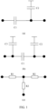
- FIG. 1(a) to FIG. 1(c) are schematic diagrams of a topology of a matching circuit according to some embodiments of this application.
- the topology of the matching circuit may be L-shaped.
- a capacitor C1 and a capacitor C2 form a structure similar to an L shape.
- the topology of the matching circuit may be Pi-shaped.
- a capacitor C1, a capacitor C2, and a capacitor C3 jointly form a structure similar to a Pi shape.
- the topology of the matching circuit may be T-shaped.
- a resistor R1, a resistor R2, and a resistor R3 jointly form a structure similar to a T shape.
- FIG. 1 merely provides an example description of a matching circuit structure.
- the matching circuit may include components different from those shown in FIG. 1 .
- This application provides a radio frequency front-end device and an electronic device including the radio frequency front-end device.
- the radio frequency front-end device provided in embodiments of this application can reduce a quantity of switches in an antenna switch and has good tuning performance.
- the electronic device provided in this application may be any one of electronic devices having a wireless communication function, such as a mobile phone, a tablet computer, a notebook computer, a wearable device, a super netbook, an ultra mobile personal computer (ultra mobile personal computer, UMPC), and a personal digital assistant (personal digital assistant, PDA).
- UMPC ultra mobile personal computer
- PDA personal digital assistant
- FIG. 2 is a schematic diagram of the mobile phone 1 according to an embodiment of this application, where FIG. 2(a) is a three-dimensional view of the mobile phone 1, and FIG. 2(b) is an exploded view of the mobile phone 1.
- the mobile phone 1 includes an antenna module 10, a baseband chip 20, a display 30, and a rear cover 40.
- the display 30 and the rear cover 40 may jointly define an accommodating space 50.
- the antenna module 10 and the baseband chip 20 are both located in the accommodating space 50.
- the antenna module 10 and the baseband chip 20 are arranged on a housing 50.
- the antenna module 10 may be connected to the baseband chip 20, to implement a wireless communication function of the mobile phone 1.
- the baseband chip may send a to-be-sent wireless signal (in a digital form) to the antenna module.
- the antenna module converts a wireless signal into an electromagnetic wave and transmits the signal into a space.
- the antenna module may receive an electromagnetic wave signal in a space, convert the signal into a digital signal that may be read by the baseband chip, and send the digital signal to the baseband chip.
- the signal sending process and the data receiving process are inverse processes.
- the technical solutions of this application are described below by using the signal receiving process as an example. However, it may be understood that technical principles and effects of this application may also be applied to the signal sending process.
- FIG. 3 is an example structural diagram of an antenna module 10 in the mobile phone 1 according to an embodiment of this application.
- the antenna module 10 includes an antenna 100, a radio frequency front-end device 200, and a transceiver 300.
- the antenna 100, the radio frequency front-end device 200, the transceiver 300, and the baseband chip 20 are connected in sequence.
- the antenna 100 is configured to receive an electromagnetic wave signal in a space and convert the electromagnetic wave signal into a radio frequency signal. Next, the antenna transmits the radio frequency signal to the radio frequency front-end device.
- One or more sets of antennas 100 may be arranged. Each set of antennas 100 may be in a form of a single antenna, an array antenna, or the like.
- the radio frequency front-end device 200 may perform filtering on a received radio frequency signal, and then transmit a filtered signal to the transceiver 300. Then the transceiver 300 may perform further processing on the received radio frequency signal (such as amplification and A/D conversion) to convert the radio frequency signal into a baseband signal. Next, the transceiver 300 transmits the baseband signal to the baseband chip 20. Then the baseband chip 20 performs decoding on the baseband signal to extract useful information or data, for example, data representing user data or control information such as a voice, a text, and a video.
- the mobile phone 1 may perform wireless communication with a network device (such as a server and a base station) or another electronic device through the antenna module 10 shown in FIG. 3 , to complete an information exchange with the network device or the another electronic device.
- a network device such as a server and a base station
- another electronic device through the antenna module 10 shown in FIG. 3 , to complete an information exchange with the network device or the another electronic device.
- the radio frequency front-end device 200 which is an important part of the antenna module 10, is a core component configured to implement a wireless communication function between the mobile phone 1 and other types of mobile terminals.
- FIG. 4 is a schematic structural diagram of a radio frequency front-end device 200a according to some technical solutions.
- the radio frequency front-end device 200a includes an antenna switch ASW, seven filters F 1a -F 7a , and a common signal terminal ANT.
- the antenna switch ASW includes seven switches S 1a -S 7a .
- Operating bands of the seven filters F 1a -F 7a are respectively a B1 band, a B3 band, a B7 band, a B40 band, a B41 band, a B39 band, and a B32 band.
- the switches S 1a -S 7a are respectively in one-to-one correspondence with the filters F 1a -F 7a .
- An end of each of the switches S 1a -S 7a is connected to the common signal terminal ANT, and another end is connected to a corresponding one of the filters F 1a -F 7a , to form a plurality of transceiver links.
- a first end a1 of the switch S 1a is connected to the common signal terminal ANT, and a second end b1 thereof is connected to the filter F 1a , to form a transceiver link for a signal in the B1 band (which is referred to as a B1 link below).
- the switch S 2a and the switch S 1a share the first end a1, and a second end b2 of the switch S 2a is connected to the filter F 2a , to form a transceiver link for a signal in the B3 band (which is referred to as a B3 link below).
- a transceiver link for a signal in the B7 band (which is referred to as a B7 link below), a transceiver link for a signal in the B40 band (which is referred to as a B40 link below), a transceiver link for a signal in the B41 band (which is referred to as a B41 link below), a transceiver link for a signal in the B39 band (which is referred to as a B39 link below), and a transceiver link for a signal in the B32 band (which is referred to as a B32 link below) may be formed.
- the antenna switch ASW may implement carrier aggregation on at least any two of the B1 signal, the B3 signal, the B7 signal, the B32 signal, the B39 signal, the B40 signal, and the B41 signal.
- the switch S 1a , the switch S 2a , and the switch S 3a of the antenna switch ASW are simultaneously turned on (in other words, a multi-way function of the antenna switch is performed)
- the B1 link, the B3 link, and the B7 link are turned on
- the foregoing radio frequency front-end device 200a can implement carrier aggregation on the B1 signal, the B3 signal, and the B7 signal.
- matching circuits ⁇ 1- ⁇ 7 are further respectively arranged between the switches S 1a -S 7a and the corresponding filters.
- the switches are respectively connected to the corresponding filters through the matching circuits.
- the second end b1 of the switch S 1a is connected to the filter F 1a through the matching circuit ⁇ 1.
- the second end b2 of the switch S 2a is connected to the filter F 2a through the matching circuit ⁇ 2.
- connection manners of the remaining matching circuits ⁇ 3- ⁇ 7 refer to FIG. 4 . Details are not described herein.
- the B1 link and the B3 link may cause a leakage of the B7 signal.
- the matching circuit ⁇ 1 and the matching circuit ⁇ 2 the B1 link and the B3 link may be brought into a high impedance state relative to the B7 signal, so as to reduce the leakage of the B7 signal from the B1 link and the B3 link.
- topologies of the matching circuits corresponding to the B1 signal and the B3 signal may be adjusted.
- different matching circuits may be needed in a carrier aggregation state and in a non-carrier aggregation state.
- the B1 link may cause a leakage of the B32 signal.
- the topology of the matching circuit of the B1 link needs to be adjusted. Therefore, a matching circuit ⁇ 8 and a switch S8a are further arranged between the switch S 1a and the filter F 1a .
- An end of the matching circuit ⁇ 8 is separately connected to the second end b1 of the switch S 1a and the matching circuit ⁇ 1 through the switch S 8a .
- the switch S 8a In the non-carrier aggregation state, the switch S 8a is turned off, the matching circuit ⁇ 1 forms the matching circuit of the B1 link, and the topology of the matching circuit ⁇ 1 may be L-shaped.
- the switch S 8a When the B1 signal and the B32 signal are in the carrier aggregation state, the switch S 8a is turned on, and the matching circuit ⁇ 1 and the matching circuit ⁇ 8 jointly form the matching circuit of the B1 link.
- the topology of the matching circuit may be Pi-shaped, so that the B1 link is brought into a high impedance state relative to the B32 signal, thereby avoiding the problem of the leakage of the B32 signal.
- the other components than the filter F 7a and the matching circuit ⁇ 7 may be integrated on a same circuit board (such as a circuit board 220a) or on a same chip.
- the other components are referred to as a radio frequency module 210a.
- the filter F7a and the matching circuit ⁇ 7 are arranged outside the radio frequency module 210a.
- this application provides a radio frequency front-end device.
- a quantity of switches in an antenna switch ASW is reduced, so that an area and a parasitic capacitance of the antenna switch ASW are reduced, thereby improving operating performance of the antenna switch ASW.
- free tuning of a matching circuit can be achieved, which meets carrier aggregation demands in different application scenarios.
- FIG. 5 is a schematic structural diagram of the radio frequency front-end device 200 according to an embodiment of this application.
- the radio frequency front-end device 200 includes the radio frequency module 210, a circuit board 220, and a filter F 7 (serving as a "first external filter") and a matching circuit ⁇ 8 (serving as a "first external matching circuit") arranged outside the radio frequency module 210.
- the radio frequency module 210 is integrated on the circuit board 220.
- the radio frequency module 210 may be integrated on a same chip. In this way, the radio frequency module may be used as an electronic component that may be purchased or sold alone.
- the radio frequency module 210 includes an antenna switch ASW, filters F 1 -F 6 , matching circuits ⁇ 1- ⁇ 6, and a common signal terminal ANT.
- the antenna switch ASW includes six switches S 1 -S 6 .
- the switches S 1 -S 6 are in one-to-one correspondence with the filters F 1 -F 6 .
- the matching circuits ⁇ 1- ⁇ 7 are also in one-to-one correspondence the filters F 1 -F 6 .
- An end of each of the switches S 1 -S 6 is connected to the common signal terminal ANT, and another end is connected to a corresponding filter through each matching circuit, so as to form a plurality of transceiver links of the radio frequency front-end device 200.
- Each transceiver link may be configured to support transceiving of a radio frequency signal in a different band.
- a first end a1 of the switch S 1 (serving as a “first switch") is connected to the common signal terminal ANT, and a second end b1 is connected to the filter F 1 (serving as a "first filter”) through the matching circuit ⁇ 1 (serving as a "first internal matching circuit”).
- An operating band of the filter F 1 may be a B1 band, to form a B1 link.
- Operating bands of F 3 -F 6 are respectively a B7 band, a B40 band, a B41 band, and a B39 band. It may be understood that the operating bands of F 3 -F 6 in FIG. 5 are merely an example description. In another embodiment, the operating bands of the filters F 3 -F 6 may be any other wireless communication band.
- FIG. 5 merely shows some example structural components included in the radio frequency module 210. Actual structures and locations of these structural components are not limited to FIG. 5 .
- the radio frequency module 210 may have more or fewer structural components than the structural components shown in FIG. 5 .
- the radio frequency module 210 may further include more filters and matching circuits corresponding to the filters, and the antenna switch ASW may further include more switches to form more transceiver links.
- the radio frequency module 210 may not include any one or more of the matching circuits ⁇ 1- ⁇ 6.
- each matching circuit may be a phase-shift matching circuit.
- connection manners and operating principles of the filter F 7 and the matching circuit ⁇ 8 in the technical solution of this application are first described by using examples in combination with the B1 link.
- the radio frequency module 210 further includes a switch S 7 (serving as a "second switch").
- the filter F 7 and the matching circuit ⁇ 8 are separately connected to the second end b1 of the switch S 1 through the switch S 7 .
- the second end b1 of the switch S 1 is connected to a first end a7 of the switch S 7
- the filter F 7 and the matching circuit ⁇ 8 are separately connected to the second end b7 of the switch S 7 .
- An operating band of the filter F 7 may be flexibly set based on demands of different countries or regions. This is not limited in this application.
- the technical solution of this application is described below by using an example in which the operating band of the filter F 7 is a B32 band.
- the switch S 1 , the switch S 7 , and the filter F 7 jointly form a B32 link.
- the B32 link may further include a matching circuit ⁇ 7, and the second end b7 of the switch S 7 is connected to the filter F 7 through the matching circuit ⁇ 7.
- the B32 link may not include the matching circuit ⁇ 7.
- the radio frequency front-end device 200 can implement carrier aggregation on the B1 signal and the B32 signal.
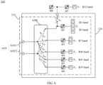
- the filter F 7 may be directly removed. Referring to FIG. 6 , when the switch S 7 is turned off, the B32 link is turned off, and the matching circuit ⁇ 8 is disconnected from the matching circuit ⁇ 1.
- the filter F 7 may be removed from the radio frequency front-end device 200, to avoid an unnecessary space waste, thereby effectively reducing manufacturing costs.
- the operating band of the filter may be set to another operating band (such as a B29 band), or the filter F 7 may be replaced with another filter.
- a quantity of switches in the antenna switch ASW is reduced from seven switches to six switches, and an area occupied by and a parasitic capacitance of the antenna switch ASW are reduced. Therefore, operating performance and integration of the radio frequency front-end device 200 are improved.
- the effect of reducing the quantity of switches of the antenna switch ASW is merely described by using an example in which the antenna switch ASW is connected to a set of antennas 100 through one common signal terminal ANT.
- the radio frequency front-end device 200 may be connected to a plurality of sets of antennas 100 respectively through a plurality of common signal terminals ANT.
- the antenna switch ASW has fewer switches.
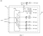
- FIG. 7 is a schematic structural diagram of a radio frequency front-end device 200 having two common signal terminals ANT according to some embodiments of this application.
- FIG. 8(a) is a schematic structural diagram of an antenna switch ASW in the radio frequency front-end device 200 in FIG. 6 .
- FIG. 8(b) is a schematic structural diagram of an antenna switch ASW according to another technical solution.
- the radio frequency module 210 includes a first common signal terminal ANT1 and a second common signal terminal ANT2.
- the first common signal terminal ANT1 and the second common signal terminal ANT2 may be respectively connected to a set of antennas (not shown in the figure).
- the antenna switch ASW of the radio frequency front-end device 200 includes ten switches S 11 -S 52 . Five switches S 11 , S 21 , S 31 , ..., S 51 are connected to the first common signal terminal ANT1, and five switches S 12 , S 22 , S 32 , ..., S 52 are connected to the second common signal terminal ANT2.
- FIG. 1 the example shown in FIG.
- the antenna switch ASW includes twelve switches S 11a -S 62a . Compared with the antenna switch ASW in the another technical solution, two fewer switches are used in the antenna switch ASW in this application, the antenna switch ASW occupies a smaller area, and each switch generates smaller parasitic capacitances at the first common signal terminal ANT1 and the second common signal terminal ANT2.
- the radio frequency front-end device 200 may alternatively include more common signal terminals ANT, such as three, four, or five common signal terminals.
- a larger quantity of common signal terminals ANT leads to a larger quantity by which switches of the antenna switch ASW in the radio frequency front-end device 200 are reduced and a larger area that is reduced.
- the foregoing switch S 7 can further change the topology of the matching circuit of the B1 link, to ensure signal transmission performance of the B1 signal and another signal (such as the B32 signal) in the carrier aggregation state and in the non-carrier aggregation state.
- the B1 link is brought into a high impedance state relative to the B32 signal, which greatly reduces a possibility that the B32 signal leaks through the B1 link, thereby improving carrier aggregation performance of the radio frequency front-end device 200.
- the matching circuit ⁇ 8 is arranged outside the radio frequency module 210, different matching circuits ⁇ 8 may be flexibly selected for different filters F 7 , which effectively increases a tuning freedom degree of the matching circuit.
- the foregoing radio frequency module 210 may further include a switch S 8 (serving as a "third switch").
- FIG. 9 is a schematic diagram of the switch S 8 in the radio frequency module 210 in the radio frequency device 200 according to some embodiments of this application.
- the second end b1 of the switch S 1 and the first end a7 of the switch S 7 are separately connected to a first end a8 of the switch S 8 , and the matching circuit ⁇ 1 is connected to a second end b8 of the switch S 8 .
- the second end b1 of the switch S 1 and the first end a7 of the switch S 7 are separately connected to the matching circuit ⁇ 1 through the switch S 8 .
- the circuit board 220 may further include a first pin 221.
- the filter F 7 and the matching circuit ⁇ 8 are separately connected to the second end b7 of the switch S 7 through the first pin 221.
- the filters F 1 -F 7 each may be either a surface acoustic wave (Surface Acoustic Wave, SAW) filter or a bulk acoustic wave (Bulk Acoustic Wave, BAW) filter.
- SAW Surface Acoustic Wave
- BAW Bulk Acoustic Wave
- the filters F 1 -F 7 each may have a plurality of different operating bands.
- the filter F 1 shown in FIG. 6 and FIG. 7 is used as an example.
- the filter F 1 has two operating bands, namely, the B1 band and the B3 band.
- the layouts of the filter F 7 , the matching circuit ⁇ 8, the switch S 7 , and the switch S 8 are merely example descriptions of the technical solutions of this application, and a person skilled in the art may make another modification.
- the filter F 7 , the matching circuit ⁇ 8, the switch S 7 , and the switch S 8 can implement the carrier aggregation on the B1 signal and the B32 signal.
- the radio frequency front-end device 300 may further include more components (for example, more switches, filters, and matching circuits) to implement carrier aggregation on signals in more bands to adapt to more different application scenarios.
- the radio frequency module 210 may have a plurality of links for aggregation with the B32 link.
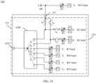
- FIG. 10 is an example structural diagram of the radio frequency front-end device 200 according to an embodiment. As shown in FIG. 10 , the first end a1 of the switch S 2 (serving as a "fourth switch") of the antenna switch ASW of the radio frequency front-end device 200 is connected to the common signal terminal ANT, and the second end b2 is connected to the filter F 2 (serving as a "second filter”) through the matching circuit ⁇ 2.
- the radio frequency module 210 further includes a switch S 9 (serving as a "fifth switch").
- the second end b2 of the switch S 2 is connected to a first end a9 of the switch S 9 , and the filter F 7 and the matching circuit ⁇ 8 are separately connected to a second end b9 of the switch S 9 .
- the filter F 7 and the matching circuit ⁇ 8 are separately connected to the second end b2 of the switch S 2 through the switch S 9 .
- the operating band of the filter F 2 may be the B3 band.
- the switch S 2 and the filter F 2 jointly form the B3 link.
- the operating band of the filter F 7 may be the B32 band.
- the switch S 2 , the switch S 9 , and the filter F 7 jointly form a B32 RX.
- the radio frequency front-end device 200 can implement carrier aggregation on the B3 signal and the B32 signal.
- the radio frequency module 210 may further include a switch S 10 (serving as a "sixth switch").
- the second end b2 of the switch S 2 and the first end a9 of the switch S 9 are separately connected to a first end a10 of the switch S 10 , and the matching circuit ⁇ 2 is connected to a second end b10 of the switch S 10 .
- the switch S 10 Through the switch S 10 , the signal transmission performance of the radio frequency front-end device 200 in the carrier aggregation state can be further improved.
- An operating principle of the switch S 10 is the same as the operating principle of the foregoing switch S 8 , and therefore is not described in detail herein.
- another link in the radio frequency module 210 may be aggregated with the B32 link, which are arranged in a manner substantially the same as the arrangement manner of the foregoing B1 link and B3 link.
- the radio frequency front-end device 200 may further include another external filter and external matching circuit arranged outside the radio frequency module 210 to adapt to carrier aggregation demands in different scenarios.
- the radio frequency front-end device may further include a second external filter and a second external matching circuit arranged outside the radio frequency module 210.
- a connection manner between the second external filter and the second external matching circuit and the radio frequency module 210 is the same as the connection manner between the foregoing filter F 7 and matching circuit ⁇ 8 and the radio frequency module 210, and therefore is not described in detail herein.
- an operating band of the second external filter may be set based on an actual need.
- the operating band of the second external filter may be the B29 band.
- the radio frequency front-end device 200 can implement carrier aggregation on another signal (such as the B1 signal, the B3 signal, and the B7 signal) and the B29 signal.
- the radio frequency front-end device 200 provided in this application, a layout of switches is redesigned, which effectively reduces the area and the parasitic capacitance of the antenna switch ASW.
- the matching circuit and the filter are arranged outside the radio frequency module, which improves a tuning freedom degree, thereby enabling the radio frequency front-end device to adapt to signals in different bands, and ensures operating performance in a carrier aggregation state of signals in different bands, thereby expanding an application range of the radio frequency front-end device 200.
Landscapes
- Engineering & Computer Science (AREA)
- Computer Networks & Wireless Communication (AREA)
- Signal Processing (AREA)
- Transceivers (AREA)
Abstract
Description
- This application claims priority to
Chinese Patent Application No. 202223555957.1, filed with the China National Intellectual Property Administration on December 27, 2022 - This application relates to the field of radio frequency technologies, and in particular, to a radio frequency front-end device, an antenna module, and an electronic device.
- As wireless communication technologies (such as 5G) develop, to meet a demand for increasing a single-user peak rate and a system capacity, a transmission bandwidth in a radio frequency front-end device in an electronic device is usually increased through a carrier aggregation (Carrier Aggregation, CA) technology. To meet demands in different carrier aggregation states, an antenna switch (Antenna Switch, ASW) in the radio frequency front-end device usually includes a plurality of switches. The plurality of switches are respectively connected to filters with different operating bands in one-to-one correspondence. However, an existing antenna switch has many switches and complex circuits, which causes a high parasitic capacitance. In addition, a current radio frequency front-end device has poor tuning performance.
- To resolve the foregoing technical problems, this application provides a radio frequency front-end device, an antenna module, and an electronic device. A layout of switches is redesigned, which effectively reduces an area and a parasitic capacitance of an antenna switch. In addition, a matching circuit and a filter are arranged outside a radio frequency module, which improves a tuning freedom degree, thereby enabling the radio frequency front-end device to adapt to signals in different bands, and ensures operating performance in a carrier aggregation state of signals in different bands, thereby expanding an application range of the radio frequency front-end device.
- According to a first aspect, this application provides a radio frequency front-end device. The radio frequency front-end device includes a radio frequency module and a first external filter and a first external matching circuit arranged outside the radio frequency module. The radio frequency module includes an antenna switch and a first filter, the antenna switch includes a first switch, a first end of the first switch is configured to connect to a common signal terminal of the radio frequency module, and a second end is connected to the first filter. The radio frequency module further includes a second switch, a first end of the second switch is connected to the second end of the first switch, and the first external filter and the first external matching circuit are separately connected to a second end of the second switch.
- In the radio frequency front-end device, the matching circuit and the filter are arranged outside the radio frequency module, so that an area and a parasitic capacitance of the antenna switch can be effectively reduced, thereby improving operating performance of the antenna switch. In addition, free tuning of the matching circuit can be achieved, which meets carrier aggregation demands in different application scenarios.
- In a possible implementation of the first aspect, the first switch is connected to the first filter through a first internal matching circuit arranged in the radio frequency module, and the first internal matching circuit has a first topology.
- In a possible implementation of the first aspect, when the second switch is turned on, the first internal matching circuit and the first external matching circuit jointly form a matching circuit having a second topology, and the second topology is different from the first topology.
- The above matching circuit has a high tuning freedom degree, and the matching circuit having different topologies can ensure signal transmission performance in a carrier aggregation state and a non-carrier aggregation state, and reduce a signal leakage possibility in the carrier aggregation state.
- In a possible implementation of the first aspect, a third switch is further arranged between the second end of the first switch and the first filter, and the third switch is configured to control connection or disconnection between the second end of the first switch and the first filter.
- In a carrier aggregation state of a plurality of signals, the third switch can effectively avoid interference between the signals, which effectively improves signal transmission performance of the radio frequency front-end device in the carrier aggregation state.
- In a possible implementation of the first aspect, the radio frequency module is integrated on a same circuit board or a same chip. In this way, the radio frequency module may be used as an electronic component that may be purchased or sold alone.
- In a possible implementation of the first aspect, the circuit board includes a first pin, and the first external filter and the first external matching circuit are separately connected to the second end of the second switch through the first pin.
- In a possible implementation of the first aspect, the radio frequency front-end device further includes a second external filter and a second external matching circuit arranged outside the radio frequency module. The radio frequency module further includes a second filter. The antenna switch further includes a fourth switch, a first end of the fourth switch is configured to connect to the common signal terminal of the radio frequency module, and a second end is connected to the second filter. The radio frequency module further includes a fifth switch, a first end of the fifth switch is connected to the second end of the fourth switch, and the second external filter and the second external matching circuit are separately connected to a second end of the fifth switch.
- In the implementations of this application, more switches (such as the fourth switch and the fifth switch), an external filter (such as the second external filter), and an external matching circuit (such as the second external matching circuit) are arranged, so that the radio frequency front-end device can achieve carrier aggregation of signals in more bands, to adapt to more different application scenarios. In this way, an application range of the radio frequency front-end device is expanded.
- In a possible implementation of the first aspect, an operating band of the first filter includes one of the following: a B1 band, a B3 band, and a B7 band; and/or an operating band of the first external filter includes a B32 band.
- In a possible implementation of the first aspect, the radio frequency module includes one or more common signal terminals.
- According to a second aspect, this application provides an antenna module. The antenna module includes an antenna, a transceiver, and the radio frequency front-end device according to any one of the implementations of the first aspect. The common signal terminal of the radio frequency front-end device is connected to the antenna, and the filter of the radio frequency front-end device is connected to the transceiver.
- According to a third aspect, this application provides an electronic device. The electronic device includes a housing and the antenna module according to the second aspect. The antenna module is arranged on the housing.
- It may be understood that the electronic device may perform wireless communication with a network device (such as a server and a base station) or another electronic device through the antenna module, to complete an information exchange with the network device or the another electronic device.
-
-
FIG. 1(a) to FIG. 1(c) are schematic diagrams of a topology of a matching circuit according to some embodiments of this application; -
FIG. 2 is a schematic diagram of a mobile phone according to an embodiment of this application, whereFIG. 2(a) is a three-dimensional view of the mobile phone, andFIG. 2(b) is an exploded view of the mobile phone; -
FIG. 3 is an example structural diagram of an antenna module in the mobile phone according to an embodiment of this application; -
FIG. 4 is a schematic structural diagram of a radio frequency front-end device according to some technical solutions; -
FIG. 5 is a schematic structural diagram of a radio frequency front-end device according to an embodiment of this application; -
FIG. 6 is an example structural diagram of a radio frequency front-end device with a filter F7 being removed according to some embodiments of this application; -
FIG. 7 is a schematic structural diagram of a radio frequency front-end device having two common signal terminals ANT according to some embodiments of this application; -
FIG. 8(a) is a schematic structural diagram of an antenna switch ASW in the radio frequency front-end device inFIG. 6 ; -
FIG. 8(b) is a schematic structural diagram of an antenna switch ASW according to another technical solution; -
FIG. 9 is a schematic diagram of a switch S8 in a radio frequency module in the radio frequency device according to some embodiments of this application; and -
FIG. 10 is an example structural diagram of the radio frequency front-end device according to an embodiment. - DESCRIPTION OF REFERENCE NUMERALS: 1-Mobile phone; 10-Antenna module; 100-Antenna; 200-Radio frequency front-end device; 210-Radio frequency module; ASW-Antenna switch; S1-S10-Switch; S11-S52-Switch; a1-First end; a7-a10-First end; b1-b10-Second end; F1-F7-Filter; Ø1-Ø8-Matching circuit; 220-Circuit board; 221-First pin; ANT-Common signal terminal; ANT1-Common signal terminal; ANT2-Common signal terminal; 200a-Radio frequency front-end device; 210a-Radio frequency module; S1a-Ss8-Switch; S11a-S62a-Switch; F1a-F7a-Filter; 220a-Circuit board; 300-Transceiver; 20-Baseband chip; 30-Display; 40-Middle frame; 50-Housing.
- To make objectives, technical solutions, and advantages of this application clearer, implementations of this application are further described in detail below with reference to drawings.
- It should be understood that "a plurality of" mentioned in this application means two or more. In the descriptions of this application, unless otherwise specified, "/" means "or". For example, A/B may mean A or B. In this specification, "and/or" merely describes an association relationship between associated objects, and indicates that three relationships may exist. For example, A and/or B may indicate the following three cases: only A exists, both A and B exist, and only B exists. Moreover, for ease of describing the technical solutions of this application clearly, terms such as "first" and "second" are used for distinguishing between same or similar items with substantially same functions and effects. A person skilled in the art may understand that the terms such as "first" and "second" do not limit a quantity or an execution sequence, and the terms such as "first" and "second" unnecessarily define a difference.
- For ease of understanding the technical solutions of this application, some technical terms and related concepts involved in embodiments of this application are first described.
- As wireless communication technologies develop, communication may be performed in a plurality of different wireless communications standards, such as 3G, 4G (or referred to as "LTE"), 5G, and Wi-Fi. Different communication standards have different operating bands. For example, a partial operating band of the 3G standard is in a range of 2010-2025 MHz, and a partial operating band of the 5G standard is in a range of 4800-4900 MHz.
- A same communication system may include a plurality of sub-bands. Table 1 shows example sub-bands in the LTE standard. Referring to Table 1, the LTE standard includes a plurality of sub-bands. Each sub-band may be represented by a band number in a format of "Bx". For example, an uplink band range "1920-1980 MHz" and a downlink band range "2110-2170 MHz" may be represented by a band number of B1.
Table 1 Sub-bands of the LTE standard Bx Uplink band (i.e., transmitting band) Downlink band (i.e., receiving band) B1 1920-1980 MHz 2110-2170 MHz B3 1710-1785 MHz 1805-1880 MHz B7 2500-2570 MHz 2620-2690 MHz B29 - 717-728 MHz B32 - 1452-1496 MHz B39 1880-1920 MHz 1880-1920 MHz B40 2300-2400 MHz 2300-2400 MHz B41 2496-2690 MHz 2496-2690 MHz - In a practical application, different countries or regions or different operators in a same country may use different operating bands. For example, an LTE band used by an operator A is a B1/B3 band, and an LTE band used by an operator B is a
B 1/B7 band. For example, some operators in Europe require a terminal device to support a B32 band, while others do not. - It is a technology in which a plurality of carriers are combined to simultaneously transmit data on the plurality of carriers. For example, a plurality of middle high bands (Middle High Band, MHB) (such as the B1 band, the B2 band, and the B7 band) are aggregated. The carrier aggregation technology can increase a transmission bandwidth, thereby increasing a data transmission rate.
- The matching circuit is configured to adjust an impedance characteristic of an electromagnetic wave transmission link, to improve transmission efficiency of a transmission link. The matching circuit is generally composed of one or more passive devices. For example, the matching circuit may be composed of one or more inductors. The inductors may be implemented by a winding inductor, a substrate inductor, or an on-chip inductor. For another example, the matching circuit may be composed of one or more capacitors. The capacitors may be implemented by a ceramic capacitor, a substrate capacitor, or an on-chip capacitor.
- The matching circuit may have a plurality of different topologies, to meet signal transmission demands in a carrier aggregation state and a non-carrier aggregation state.
FIG. 1(a) to FIG. 1(c) are schematic diagrams of a topology of a matching circuit according to some embodiments of this application. For example, as shown inFIG. 1(a) , the topology of the matching circuit may be L-shaped. In other words, a capacitor C1 and a capacitor C2 form a structure similar to an L shape. For another example, as shown inFIG. 1(b) , the topology of the matching circuit may be Pi-shaped. In other words, a capacitor C1, a capacitor C2, and a capacitor C3 jointly form a structure similar to a Pi shape. For example, as shown inFIG. 1(c) , the topology of the matching circuit may be T-shaped. In other words, a resistor R1, a resistor R2, and a resistor R3 jointly form a structure similar to a T shape. In addition, it may be understood thatFIG. 1 merely provides an example description of a matching circuit structure. In another embodiment, the matching circuit may include components different from those shown inFIG. 1 . - Implementations of this application are further described in detail below with reference to the drawings.
- This application provides a radio frequency front-end device and an electronic device including the radio frequency front-end device. The radio frequency front-end device provided in embodiments of this application can reduce a quantity of switches in an antenna switch and has good tuning performance.
- It may be understood that the electronic device provided in this application may be any one of electronic devices having a wireless communication function, such as a mobile phone, a tablet computer, a notebook computer, a wearable device, a super netbook, an ultra mobile personal computer (ultra mobile personal computer, UMPC), and a personal digital assistant (personal digital assistant, PDA). For ease of description, the solution is described below by using an example in which the electronic device is a mobile phone.
-
FIG. 2 is a schematic diagram of themobile phone 1 according to an embodiment of this application, whereFIG. 2(a) is a three-dimensional view of themobile phone 1, andFIG. 2(b) is an exploded view of themobile phone 1. Referring toFIG. 2 , themobile phone 1 includes anantenna module 10, abaseband chip 20, adisplay 30, and arear cover 40. - The
display 30 and therear cover 40 may jointly define anaccommodating space 50. Theantenna module 10 and thebaseband chip 20 are both located in theaccommodating space 50. For example, theantenna module 10 and thebaseband chip 20 are arranged on ahousing 50. Theantenna module 10 may be connected to thebaseband chip 20, to implement a wireless communication function of themobile phone 1. For example, in a data sending process, the baseband chip may send a to-be-sent wireless signal (in a digital form) to the antenna module. The antenna module converts a wireless signal into an electromagnetic wave and transmits the signal into a space. In a signal receiving process, the antenna module may receive an electromagnetic wave signal in a space, convert the signal into a digital signal that may be read by the baseband chip, and send the digital signal to the baseband chip. - The signal sending process and the data receiving process are inverse processes. The technical solutions of this application are described below by using the signal receiving process as an example. However, it may be understood that technical principles and effects of this application may also be applied to the signal sending process.
-
FIG. 3 is an example structural diagram of anantenna module 10 in themobile phone 1 according to an embodiment of this application. Referring toFIG. 3 , theantenna module 10 includes anantenna 100, a radio frequency front-end device 200, and atransceiver 300. Theantenna 100, the radio frequency front-end device 200, thetransceiver 300, and thebaseband chip 20 are connected in sequence. - In the
antenna module 10, theantenna 100 is configured to receive an electromagnetic wave signal in a space and convert the electromagnetic wave signal into a radio frequency signal. Next, the antenna transmits the radio frequency signal to the radio frequency front-end device. One or more sets ofantennas 100 may be arranged. Each set ofantennas 100 may be in a form of a single antenna, an array antenna, or the like. - The radio frequency front-
end device 200 may perform filtering on a received radio frequency signal, and then transmit a filtered signal to thetransceiver 300. Then thetransceiver 300 may perform further processing on the received radio frequency signal (such as amplification and A/D conversion) to convert the radio frequency signal into a baseband signal. Next, thetransceiver 300 transmits the baseband signal to thebaseband chip 20. Then thebaseband chip 20 performs decoding on the baseband signal to extract useful information or data, for example, data representing user data or control information such as a voice, a text, and a video. - It may be understood that the
mobile phone 1 may perform wireless communication with a network device (such as a server and a base station) or another electronic device through theantenna module 10 shown inFIG. 3 , to complete an information exchange with the network device or the another electronic device. - In addition, it may be understood that the radio frequency front-
end device 200, which is an important part of theantenna module 10, is a core component configured to implement a wireless communication function between themobile phone 1 and other types of mobile terminals. -
FIG. 4 is a schematic structural diagram of a radio frequency front-end device 200a according to some technical solutions. As shown inFIG. 4 , the radio frequency front-end device 200a includes an antenna switch ASW, seven filters F1a-F7a, and a common signal terminal ANT. The antenna switch ASW includes seven switches S1a-S7a. Operating bands of the seven filters F1a-F7a are respectively a B1 band, a B3 band, a B7 band, a B40 band, a B41 band, a B39 band, and a B32 band. - The switches S1a-S7a are respectively in one-to-one correspondence with the filters F1a-F7a. An end of each of the switches S1a-S7a is connected to the common signal terminal ANT, and another end is connected to a corresponding one of the filters F1a-F7a, to form a plurality of transceiver links. For example, a first end a1 of the switch S1a is connected to the common signal terminal ANT, and a second end b1 thereof is connected to the filter F1a, to form a transceiver link for a signal in the B1 band (which is referred to as a B1 link below). For another example, the switch S2a and the switch S1a share the first end a1, and a second end b2 of the switch S2a is connected to the filter F2a, to form a transceiver link for a signal in the B3 band (which is referred to as a B3 link below). By analogy, a transceiver link for a signal in the B7 band (which is referred to as a B7 link below), a transceiver link for a signal in the B40 band (which is referred to as a B40 link below), a transceiver link for a signal in the B41 band (which is referred to as a B41 link below), a transceiver link for a signal in the B39 band (which is referred to as a B39 link below), and a transceiver link for a signal in the B32 band (which is referred to as a B32 link below) may be formed.
- The antenna switch ASW may implement carrier aggregation on at least any two of the B1 signal, the B3 signal, the B7 signal, the B32 signal, the B39 signal, the B40 signal, and the B41 signal. For example, when the switch S1a, the switch S2a, and the switch S3a of the antenna switch ASW are simultaneously turned on (in other words, a multi-way function of the antenna switch is performed), the B1 link, the B3 link, and the B7 link are turned on, and the foregoing radio frequency front-
end device 200a can implement carrier aggregation on the B1 signal, the B3 signal, and the B7 signal. - Still referring to
FIG. 4 , in the foregoing radio frequency front-end device 200a, matching circuits Ø1-Ø7 are further respectively arranged between the switches S1a-S7a and the corresponding filters. The switches are respectively connected to the corresponding filters through the matching circuits. For example, the second end b1 of the switch S1a is connected to the filter F1a through the matching circuit Ø1. For another example, the second end b2 of the switch S2a is connected to the filter F2a through the matching circuit Ø2. For connection manners of the remaining matching circuits Ø3-Ø7, refer toFIG. 4 . Details are not described herein. - Through the arrangement of the matching circuits, a problem of a signal leakage in a carrier aggregation state can be avoided, and signal transmission performance can be improved.
- For example, in a carrier aggregation state of the B1 signal, the B3 signal, and the B7 signal, the B1 link and the B3 link may cause a leakage of the B7 signal. Through the arrangement of the matching circuit Ø1 and the matching circuit Ø2, the B1 link and the B3 link may be brought into a high impedance state relative to the B7 signal, so as to reduce the leakage of the B7 signal from the B1 link and the B3 link. Similarly, topologies of the matching circuits corresponding to the B1 signal and the B3 signal may be adjusted.
- In addition, different matching circuits may be needed in a carrier aggregation state and in a non-carrier aggregation state.
- For example, in a carrier aggregation state of the B1 signal and the B32 signal, the B1 link may cause a leakage of the B32 signal. To avoid the problem of the leakage of the B32 signal, the topology of the matching circuit of the B1 link needs to be adjusted. Therefore, a matching circuit Ø8 and a switch S8a are further arranged between the switch S1a and the filter F1a. An end of the matching circuit Ø8 is separately connected to the second end b1 of the switch S1a and the matching circuit Ø1 through the switch S8a.
- In the non-carrier aggregation state, the switch S8a is turned off, the matching circuit Ø1 forms the matching circuit of the B1 link, and the topology of the matching circuit Ø1 may be L-shaped. When the B1 signal and the B32 signal are in the carrier aggregation state, the switch S8a is turned on, and the matching circuit Ø1 and the matching circuit Ø8 jointly form the matching circuit of the B1 link. The topology of the matching circuit may be Pi-shaped, so that the B1 link is brought into a high impedance state relative to the B32 signal, thereby avoiding the problem of the leakage of the B32 signal.
- Operators in different countries or regions have different demands on the carrier aggregation state. For example, a European operator needs to support receiving of a radio frequency signal in the B32 band and carrier aggregation related to the signal, while other regions do not. To meet use needs of different regions and avoid cost wastes, the other components than the filter F7a and the matching circuit Ø7 may be integrated on a same circuit board (such as a
circuit board 220a) or on a same chip. The other components are referred to as aradio frequency module 210a. The filter F7a and the matching circuit Ø7 are arranged outside theradio frequency module 210a. In other words, the foregoing radio frequency front-end device 200a may include theradio frequency module 210a and the filter F7a and the matching circuit Ø7 arranged outside theradio frequency module 210a. Theradio frequency module 210a includes the antenna switch ASW, the common signal terminal ANT, the six filters F1a-F6a, the matching circuits Ø1-Ø6, the matching circuit Ø8, and the switch S8a. - However, because of different manufacturing processes, filters F7 provided by different manufacturers have different impedance characteristics. Therefore, the filters F7 of different manufacturers requires different matching circuits Ø8. For example, when the matching circuit Ø8 is a capacitor, the different filters F7 match different capacitance values. In the manner shown in
FIG. 4 , the matching circuit Ø8 is integrated on thecircuit board 220a. In this case, matching circuits Ø8 adapting to the different filters F7 cannot be flexibly selected based on the different filters F7. As a result, a tuning freedom degree is low, and it is difficult to meet carrier aggregation demands in different operating scenarios. - In addition, in the example shown in
FIG. 4 , to control an operation of the filter F7a, the antenna switch ASW needs to include the switch S7a. As a result, the antenna switch ASW has a large quantity of switches, and therefore the antenna switch ASW occupies a large area. Besides, the large quantity of switches generate a large parasitic capacitance at the common signal terminal ANT. - To resolve the foregoing problem, this application provides a radio frequency front-end device. Through the radio frequency front-end device, a quantity of switches in an antenna switch ASW is reduced, so that an area and a parasitic capacitance of the antenna switch ASW are reduced, thereby improving operating performance of the antenna switch ASW. In addition, through the radio frequency front-end device, free tuning of a matching circuit can be achieved, which meets carrier aggregation demands in different application scenarios. A detailed description is provided below with reference to the drawings.
-
FIG. 5 is a schematic structural diagram of the radio frequency front-end device 200 according to an embodiment of this application. As shown inFIG. 5 , the radio frequency front-end device 200 includes theradio frequency module 210, acircuit board 220, and a filter F7 (serving as a "first external filter") and a matching circuit Ø8 (serving as a "first external matching circuit") arranged outside theradio frequency module 210. In this embodiment, theradio frequency module 210 is integrated on thecircuit board 220. Alternatively, in some other embodiments, theradio frequency module 210 may be integrated on a same chip. In this way, the radio frequency module may be used as an electronic component that may be purchased or sold alone. - The
radio frequency module 210 includes an antenna switch ASW, filters F1-F6, matching circuits Ø1-Ø6, and a common signal terminal ANT. The antenna switch ASW includes six switches S1-S6. The switches S1-S6 are in one-to-one correspondence with the filters F1-F6. The matching circuits Ø1-Ø7 are also in one-to-one correspondence the filters F1-F6. An end of each of the switches S1-S6 is connected to the common signal terminal ANT, and another end is connected to a corresponding filter through each matching circuit, so as to form a plurality of transceiver links of the radio frequency front-end device 200. Each transceiver link may be configured to support transceiving of a radio frequency signal in a different band. - For example, a first end a1 of the switch S1 (serving as a "first switch") is connected to the common signal terminal ANT, and a second end b1 is connected to the filter F1 (serving as a "first filter") through the matching circuit Ø1 (serving as a "first internal matching circuit"). An operating band of the filter F1 may be a B1 band, to form a B1 link.
- For another example, a switch S2 may share the first end a1 with the switch S1, and a second end b2 is connected to the filter F2 through the matching circuit Ø2. An operating band of the filter F2 may be a B3 band, to form the B3 link.
- For connection manners among the switches S3-S6, the matching circuits Ø3-Ø6, and the filters F3-F6, refer to
FIG. 5 . Details are not described herein. Operating bands of F3-F6 are respectively a B7 band, a B40 band, a B41 band, and a B39 band. It may be understood that the operating bands of F3-F6 inFIG. 5 are merely an example description. In another embodiment, the operating bands of the filters F3-F6 may be any other wireless communication band. - It may be understood that
FIG. 5 merely shows some example structural components included in theradio frequency module 210. Actual structures and locations of these structural components are not limited toFIG. 5 . In addition, theradio frequency module 210 may have more or fewer structural components than the structural components shown inFIG. 5 . For example, theradio frequency module 210 may further include more filters and matching circuits corresponding to the filters, and the antenna switch ASW may further include more switches to form more transceiver links. For another example, in some embodiments, theradio frequency module 210 may not include any one or more of the matching circuits Ø1-Ø6. For example, each matching circuit may be a phase-shift matching circuit. - For ease of description, connection manners and operating principles of the filter F7 and the matching circuit Ø8 in the technical solution of this application are first described by using examples in combination with the B1 link.
- Still referring to
FIG. 5 , theradio frequency module 210 further includes a switch S7 (serving as a "second switch"). The filter F7 and the matching circuit Ø8 are separately connected to the second end b1 of the switch S1 through the switch S7. In other words, the second end b1 of the switch S1 is connected to a first end a7 of the switch S7, and the filter F7 and the matching circuit Ø8 are separately connected to the second end b7 of the switch S7. - An operating band of the filter F7 may be flexibly set based on demands of different countries or regions. This is not limited in this application. The technical solution of this application is described below by using an example in which the operating band of the filter F7 is a B32 band. The switch S1, the switch S7, and the filter F7 jointly form a B32 link. In addition, in this embodiment, the B32 link may further include a matching circuit Ø7, and the second end b7 of the switch S7 is connected to the filter F7 through the matching circuit Ø7. Alternatively, in another embodiment, the B32 link may not include the matching circuit Ø7.
- When the switch S1 and the switch S7 are simultaneously turned on, the radio frequency front-
end device 200 can implement carrier aggregation on the B1 signal and the B32 signal. When the B32 signal is not needed in themobile phone 1, the filter F7 may be directly removed. Referring toFIG. 6 , when the switch S7 is turned off, the B32 link is turned off, and the matching circuit Ø8 is disconnected from the matching circuit Ø1. In addition, in some embodiments, when the filter F7 is not needed in themobile phone 1, the filter F7 may be removed from the radio frequency front-end device 200, to avoid an unnecessary space waste, thereby effectively reducing manufacturing costs. Alternatively, when themobile phone 1 needs to support transceiving of a signal in another band (such as a B29 signal) and carrier aggregation related to the signal, the operating band of the filter may be set to another operating band (such as a B29 band), or the filter F7 may be replaced with another filter. - Compared with
FIG. 4 , inFIG. 5 , in the foregoing radio frequency front-end device 200, a quantity of switches in the antenna switch ASW is reduced from seven switches to six switches, and an area occupied by and a parasitic capacitance of the antenna switch ASW are reduced. Therefore, operating performance and integration of the radio frequency front-end device 200 are improved. - In the foregoing embodiments, the effect of reducing the quantity of switches of the antenna switch ASW is merely described by using an example in which the antenna switch ASW is connected to a set of
antennas 100 through one common signal terminal ANT. In some other embodiments, the radio frequency front-end device 200 may be connected to a plurality of sets ofantennas 100 respectively through a plurality of common signal terminals ANT. In this case, the antenna switch ASW has fewer switches. -
FIG. 7 is a schematic structural diagram of a radio frequency front-end device 200 having two common signal terminals ANT according to some embodiments of this application.FIG. 8(a) is a schematic structural diagram of an antenna switch ASW in the radio frequency front-end device 200 inFIG. 6 .FIG. 8(b) is a schematic structural diagram of an antenna switch ASW according to another technical solution. - In the examples shown in
FIG. 7 andFIG. 8(a) , theradio frequency module 210 includes a first common signal terminal ANT1 and a second common signal terminal ANT2. The first common signal terminal ANT1 and the second common signal terminal ANT2 may be respectively connected to a set of antennas (not shown in the figure). The antenna switch ASW of the radio frequency front-end device 200 includes ten switches S11-S52. Five switches S11, S21, S31, ..., S51 are connected to the first common signal terminal ANT1, and five switches S12, S22, S32, ..., S52 are connected to the second common signal terminal ANT2. In the example shown inFIG. 8(b) , the antenna switch ASW includes twelve switches S11a-S62a. Compared with the antenna switch ASW in the another technical solution, two fewer switches are used in the antenna switch ASW in this application, the antenna switch ASW occupies a smaller area, and each switch generates smaller parasitic capacitances at the first common signal terminal ANT1 and the second common signal terminal ANT2. - It may be understood that the radio frequency front-
end device 200 may alternatively include more common signal terminals ANT, such as three, four, or five common signal terminals. A larger quantity of common signal terminals ANT leads to a larger quantity by which switches of the antenna switch ASW in the radio frequency front-end device 200 are reduced and a larger area that is reduced. - Still referring to
FIG. 5 , in addition to implementing the carrier aggregation between the B1 signal and the B32 signal, the foregoing switch S7 can further change the topology of the matching circuit of the B1 link, to ensure signal transmission performance of the B1 signal and another signal (such as the B32 signal) in the carrier aggregation state and in the non-carrier aggregation state. - Specifically, in the non-carrier aggregation state, the switch S7 is turned off, and the matching circuit Ø1 forms the matching circuit of the B1 link. The matching circuit Ø1 has a first topology. For example, the first topology may be L-shaped, as shown in
FIG. 1(a) . In the carrier aggregation state of B1 and B32, the switch S7 is turned on, and the matching circuit Ø1 and the matching circuit Ø8 jointly form the matching circuit of the B1 link. The matching circuit has a second topology. The second topology is different from the first topology. For example, the second topology may be Pi-shaped, as shown inFIG. 1(b) . In this case, the B1 link is brought into a high impedance state relative to the B32 signal, which greatly reduces a possibility that the B32 signal leaks through the B1 link, thereby improving carrier aggregation performance of the radio frequency front-end device 200. In addition, since the matching circuit Ø8 is arranged outside theradio frequency module 210, different matching circuits Ø8 may be flexibly selected for different filters F7, which effectively increases a tuning freedom degree of the matching circuit. - In some other embodiments, when the filter F7 is removed, the topology of the matching circuit of the B1 link may be adjusted through S7, to ensure carrier aggregation performance of the B1 signal with another signal. For example, in a carrier aggregation state of the B1 signal and the B3 signal, the switch S7 is turned on, and the topology of the matching circuit of the B1 link changes from the first topology (for example, is L-shaped) to the second topology (for example, is Pi-shaped). Therefore, the B1 link is brought into a high impedance state relative to the B3 signal, which reduces a possibility that the B3 signal leaks through the B1 link.
- To further improve the signal transmission performance in the carrier aggregation state, the foregoing
radio frequency module 210 may further include a switch S8 (serving as a "third switch").FIG. 9 is a schematic diagram of the switch S8 in theradio frequency module 210 in theradio frequency device 200 according to some embodiments of this application. - As shown in
FIG. 9 , the second end b1 of the switch S1 and the first end a7 of the switch S7 are separately connected to a first end a8 of the switch S8, and the matching circuit Ø1 is connected to a second end b8 of the switch S8. In other words, the second end b1 of the switch S1 and the first end a7 of the switch S7 are separately connected to the matching circuit Ø1 through the switch S8. - The switch S8 can control connection or disconnection between the switch S1 and the filter F1. Specifically, when carrier aggregation between signals other than the B1 signal and the B32 signal is needed, the switch S8 may be turned off to avoid interference among the signals. For example, in a carrier aggregation state of the B3 signal and the B32 signal, the switch S1, the switch S2, and the switch S7 are turned on, and the switch S8 is turned off. In other words, the B1 link is turned off, and the B3 link and the B32 link are turned on. In this way, it is ensured that the B1 link does not cause interference to transmission of the B3 signal and the B32 signal, thereby effectively improving the signal transmission performance of the radio frequency front-
end device 200 in the carrier aggregation state. - In some embodiments of this application, the
circuit board 220 may further include afirst pin 221. The filter F7 and the matching circuit Ø8 are separately connected to the second end b7 of the switch S7 through thefirst pin 221. - In some embodiments of this application, the filters F1-F7 each may be either a surface acoustic wave (Surface Acoustic Wave, SAW) filter or a bulk acoustic wave (Bulk Acoustic Wave, BAW) filter. The filters F1-F7 are separately connected to the foregoing
transceiver 300. - In some embodiments of this application, the filters F1-F7 each may have a plurality of different operating bands. The filter F1 shown in
FIG. 6 andFIG. 7 is used as an example. The filter F1 has two operating bands, namely, the B1 band and the B3 band. - It may be understood that the layouts of the filter F7, the matching circuit Ø8, the switch S7, and the switch S8 are merely example descriptions of the technical solutions of this application, and a person skilled in the art may make another modification. For example, in this embodiment, the filter F7, the matching circuit Ø8, the switch S7, and the switch S8 can implement the carrier aggregation on the B1 signal and the B32 signal. In another embodiment, the radio frequency front-
end device 300 may further include more components (for example, more switches, filters, and matching circuits) to implement carrier aggregation on signals in more bands to adapt to more different application scenarios. - In some embodiments, the
radio frequency module 210 may have a plurality of links for aggregation with the B32 link.FIG. 10 is an example structural diagram of the radio frequency front-end device 200 according to an embodiment. As shown inFIG. 10 , the first end a1 of the switch S2 (serving as a "fourth switch") of the antenna switch ASW of the radio frequency front-end device 200 is connected to the common signal terminal ANT, and the second end b2 is connected to the filter F2 (serving as a "second filter") through the matching circuit Ø2. Theradio frequency module 210 further includes a switch S9 (serving as a "fifth switch"). The second end b2 of the switch S2 is connected to a first end a9 of the switch S9, and the filter F7 and the matching circuit Ø8 are separately connected to a second end b9 of the switch S9. In other words, the filter F7 and the matching circuit Ø8 are separately connected to the second end b2 of the switch S2 through the switch S9. - For example, the operating band of the filter F2 may be the B3 band. In this case, the switch S2 and the filter F2 jointly form the B3 link. The operating band of the filter F7 may be the B32 band. In this case, the switch S2, the switch S9, and the filter F7 jointly form a B32 RX. When the switch S2 and the switch S9 are simultaneously turned on, the radio frequency front-
end device 200 can implement carrier aggregation on the B3 signal and the B32 signal. - Similar to the foregoing switch S7, in addition to implementing the carrier aggregation between the B3 signal and the B32 signal, the switch S9 can further change the topology of the matching circuit of the B2 link, to ensure signal transmission performance of the B3 signal and another signal (such as the B32 signal) in the carrier aggregation state and in the non-carrier aggregation state. A principle of changing the topology of the matching circuit of the B2 link through the switch S9 is the same as a principle of changing the topology of the matching circuit of the B1 link through the foregoing switch S7, and therefore is not described in detail herein again.
- Still referring to
FIG. 9 , theradio frequency module 210 may further include a switch S10 (serving as a "sixth switch"). The second end b2 of the switch S2 and the first end a9 of the switch S9 are separately connected to a first end a10 of the switch S10, and the matching circuit Ø2 is connected to a second end b10 of the switch S10. Through the switch S10, the signal transmission performance of the radio frequency front-end device 200 in the carrier aggregation state can be further improved. An operating principle of the switch S10 is the same as the operating principle of the foregoing switch S8, and therefore is not described in detail herein. - In some other embodiments, another link in the radio frequency module 210 (such as the B7 link) may be aggregated with the B32 link, which are arranged in a manner substantially the same as the arrangement manner of the foregoing B1 link and B3 link.
- For another example, in some other embodiments, in addition to the foregoing filter F7 and matching circuit Ø8, the radio frequency front-
end device 200 may further include another external filter and external matching circuit arranged outside theradio frequency module 210 to adapt to carrier aggregation demands in different scenarios. For example, the radio frequency front-end device may further include a second external filter and a second external matching circuit arranged outside theradio frequency module 210. A connection manner between the second external filter and the second external matching circuit and theradio frequency module 210 is the same as the connection manner between the foregoing filter F7 and matching circuit Ø8 and theradio frequency module 210, and therefore is not described in detail herein. Similarly, an operating band of the second external filter may be set based on an actual need. For example, the operating band of the second external filter may be the B29 band. In this case, the radio frequency front-end device 200 can implement carrier aggregation on another signal (such as the B1 signal, the B3 signal, and the B7 signal) and the B29 signal. - Based on the above, according to the radio frequency front-
end device 200 provided in this application, a layout of switches is redesigned, which effectively reduces the area and the parasitic capacitance of the antenna switch ASW. In addition, the matching circuit and the filter are arranged outside the radio frequency module, which improves a tuning freedom degree, thereby enabling the radio frequency front-end device to adapt to signals in different bands, and ensures operating performance in a carrier aggregation state of signals in different bands, thereby expanding an application range of the radio frequency front-end device 200. - Obviously, a person skilled in the art may make various modifications and variations to this application without departing from the spirit and scope of this application. In this way, if the modifications and variations made to this application fall within the scope of the claims of this application and their equivalent technologies, this application is intended to include these modifications and variations.
Claims (11)
- A radio frequency front-end device, comprising a radio frequency module and a first external filter and a first external matching circuit arranged outside the radio frequency module, whereinthe radio frequency module comprises an antenna switch and a first filter, the antenna switch comprises a first switch, a first end of the first switch is configured to connect to a common signal terminal of the radio frequency module, and a second end is connected to the first filter; andthe radio frequency module further comprises a second switch, a first end of the second switch is connected to the second end of the first switch, and the first external filter and the first external matching circuit are separately connected to a second end of the second switch.
- The radio frequency front-end device according to claim 1, wherein the first switch is connected to the first filter through a first internal matching circuit arranged in the radio frequency module, and the first internal matching circuit has a first topology.
- The radio frequency front-end device according to claim 2, wherein when the second switch is turned on, the first internal matching circuit and the first external matching circuit jointly form a matching circuit having a second topology, and the second topology is different from the first topology.
- The radio frequency front-end device according to claim 1, wherein a third switch is further arranged between the second end of the first switch and the first filter, and the third switch is configured to control connection or disconnection between the second end of the first switch and the first filter.
- The radio frequency front-end device according to claim 1, wherein the radio frequency module is integrated on a same circuit board or a same chip.
- The radio frequency front-end device according to claim 5, wherein the circuit board comprises a first pin, and the first external filter and the first external matching circuit are separately connected to the second end of the second switch through the first pin.
- The radio frequency front-end device according to claim 1, further comprising a second external filter and a second external matching circuit arranged outside the radio frequency module, whereinthe radio frequency module further comprises a second filter, the antenna switch further comprises a fourth switch, a first end of the fourth switch is configured to connect to the common signal terminal of the radio frequency module, and a second end is connected to the second filter; andthe radio frequency module further comprises a fifth switch, a first end of the fifth switch is connected to the second end of the fourth switch, and the second external filter and the second external matching circuit are separately connected to a second end of the fifth switch.
- The radio frequency front-end device according to claim 1, wherein an operating band of the first filter comprises one of the following: a B1 band, a B3 band, and a B7 band; and/or an operating band of the first external filter comprises a B32 band.
- The radio frequency front-end device according to claim 1, wherein the radio frequency module comprises one or more common signal terminals.
- An antenna module, comprising an antenna, a transceiver, and the radio frequency front-end device according to any one of claims 1 to 9, wherein the common signal terminal of the radio frequency front-end device is connected to the antenna, and the filter of the radio frequency front-end device is connected to the transceiver.
- An electronic device, comprising a housing and the antenna module according to claim 10, wherein the antenna module is arranged on the housing.
Applications Claiming Priority (2)
| Application Number | Priority Date | Filing Date | Title |
|---|---|---|---|
| CN202223555957.1U CN219577051U (en) | 2022-12-27 | 2022-12-27 | Radio frequency front-end device, antenna module and electronic equipment |
| PCT/CN2023/093971 WO2024139009A1 (en) | 2022-12-27 | 2023-05-12 | Radio frequency front end device, antenna module, and electronic device |
Publications (2)
| Publication Number | Publication Date |
|---|---|
| EP4529070A1 true EP4529070A1 (en) | 2025-03-26 |
| EP4529070A4 EP4529070A4 (en) | 2025-11-05 |
Family
ID=87668585
Family Applications (1)
| Application Number | Title | Priority Date | Filing Date |
|---|---|---|---|
| EP23908957.6A Pending EP4529070A4 (en) | 2022-12-27 | 2023-05-12 | HIGH-FREQUENCY FRONT END DEVICE, ANTENNA MODULE AND ELECTRONIC DEVICE |
Country Status (4)
| Country | Link |
|---|---|
| US (1) | US20260005716A1 (en) |
| EP (1) | EP4529070A4 (en) |
| CN (2) | CN219577051U (en) |
| WO (1) | WO2024139009A1 (en) |
Families Citing this family (1)
| Publication number | Priority date | Publication date | Assignee | Title |
|---|---|---|---|---|
| CN119743162B (en) * | 2023-09-22 | 2026-02-24 | 荣耀终端股份有限公司 | Radio frequency front end module and electronic equipment |
Family Cites Families (7)
| Publication number | Priority date | Publication date | Assignee | Title |
|---|---|---|---|---|
| US9893752B2 (en) * | 2014-10-31 | 2018-02-13 | Skyworks Solutions, Inc. | Diversity receiver front end system with variable-gain amplifiers |
| US10700658B2 (en) * | 2016-02-19 | 2020-06-30 | Psemi Corporation | Adaptive tuning networks with direct mapped multiple channel filter tuning |
| CN106209120A (en) * | 2016-06-30 | 2016-12-07 | 维沃移动通信有限公司 | A kind of radio circuit and mobile terminal |
| CN109560833B (en) * | 2019-01-28 | 2022-01-11 | 惠州Tcl移动通信有限公司 | Downlink carrier aggregation radio frequency circuit, antenna device and electronic equipment |
| US11646782B2 (en) * | 2019-05-12 | 2023-05-09 | Skyworks Solutions, Inc. | Carrier aggregation circuit having multi-stage filter combination |
| CN111565057B (en) * | 2020-06-23 | 2020-10-30 | 锐石创芯(深圳)科技有限公司 | Radio frequency front-end module, antenna device and communication terminal |
| US11424769B2 (en) * | 2020-08-28 | 2022-08-23 | Qorvo Us, Inc. | Radio frequency filtering circuitry with reduced filter set |
-
2022
- 2022-12-27 CN CN202223555957.1U patent/CN219577051U/en active Active
-
2023
- 2023-05-12 EP EP23908957.6A patent/EP4529070A4/en active Pending
- 2023-05-12 US US18/880,796 patent/US20260005716A1/en active Pending
- 2023-05-12 WO PCT/CN2023/093971 patent/WO2024139009A1/en not_active Ceased
- 2023-05-12 CN CN202380022107.3A patent/CN118844038A/en active Pending
Also Published As
| Publication number | Publication date |
|---|---|
| EP4529070A4 (en) | 2025-11-05 |
| CN219577051U (en) | 2023-08-22 |
| WO2024139009A1 (en) | 2024-07-04 |
| CN118844038A (en) | 2024-10-25 |
| US20260005716A1 (en) | 2026-01-01 |
Similar Documents
| Publication | Publication Date | Title |
|---|---|---|
| US12166522B2 (en) | RF system and electronic device | |
| JP4278868B2 (en) | Harmonic rejection in dual-band mobile phones | |
| US6317608B1 (en) | Power amplifier matching in dual band mobile phone | |
| EP4270646B1 (en) | Antenna assembly and electronic device | |
| US11683054B2 (en) | Multi-band radio frequency front-end device, multi-band receiver, and multi-band transmitter | |
| CN111628802B (en) | Radio frequency circuit and electronic equipment | |
| EP4220969A1 (en) | Rf drx device, rf transceiver system, and communication apparatus | |
| EP1673949A2 (en) | Multiband multimode communication engines | |
| US8868126B2 (en) | Mobile apparatus with radio frequency architecture supporting simultaneous data and voice communications | |
| CN215682278U (en) | Radio frequency device and terminal equipment | |
| KR20220161194A (en) | Switchable acoustic wave filter and related multiplexers | |
| CN112751573A (en) | Radio frequency front-end module, transceiver and communication terminal | |
| CN118157688B (en) | Communication devices and electronic equipment | |
| US20260005716A1 (en) | Radio Frequency Front-End Device, Antenna Module, and Electronic Device | |
| US11336323B2 (en) | Front-end module and communication device | |
| CN117713865A (en) | Radio frequency front-end module and communication equipment | |
| EP3852277A1 (en) | Rf system and electronic device | |
| CN201191826Y (en) | Multi-mode mobile communication terminal and radio frequency receiver unit thereof | |
| WO2022024642A1 (en) | High-frequency module, and communication device | |
| CN215120767U (en) | Three-way antenna multiplexer applied to carrier aggregation | |
| CN211830764U (en) | Radio frequency circuit and electronic equipment | |
| CN216357508U (en) | Circuit board assembly and communication equipment | |
| JP2002290269A (en) | Hybrid high frequency component and information terminal employing it | |
| CN115548683A (en) | Antenna module and electronic equipment | |
| CN215344571U (en) | Four-multiplexer applied to carrier aggregation |
Legal Events
| Date | Code | Title | Description |
|---|---|---|---|
| STAA | Information on the status of an ep patent application or granted ep patent |
Free format text: STATUS: THE INTERNATIONAL PUBLICATION HAS BEEN MADE |
|
| PUAI | Public reference made under article 153(3) epc to a published international application that has entered the european phase |
Free format text: ORIGINAL CODE: 0009012 |
|
| STAA | Information on the status of an ep patent application or granted ep patent |
Free format text: STATUS: REQUEST FOR EXAMINATION WAS MADE |
|
| 17P | Request for examination filed |
Effective date: 20241218 |
|
| AK | Designated contracting states |
Kind code of ref document: A1 Designated state(s): AL AT BE BG CH CY CZ DE DK EE ES FI FR GB GR HR HU IE IS IT LI LT LU LV MC ME MK MT NL NO PL PT RO RS SE SI SK SM TR |
|
| REG | Reference to a national code |
Ref country code: DE Ref legal event code: R079 Free format text: PREVIOUS MAIN CLASS: H04L0005000000 Ipc: H04B0001000000 |
|
| A4 | Supplementary search report drawn up and despatched |
Effective date: 20251007 |
|
| RIC1 | Information provided on ipc code assigned before grant |
Ipc: H04B 1/00 20060101AFI20250930BHEP Ipc: H04B 1/18 20060101ALI20250930BHEP |
|
| DAV | Request for validation of the european patent (deleted) | ||
| DAX | Request for extension of the european patent (deleted) | ||
| GRAP | Despatch of communication of intention to grant a patent |
Free format text: ORIGINAL CODE: EPIDOSNIGR1 |
|
| STAA | Information on the status of an ep patent application or granted ep patent |
Free format text: STATUS: GRANT OF PATENT IS INTENDED |
|
| INTG | Intention to grant announced |
Effective date: 20260410 |