EP4529024A1 - Transceiver physical layer interface - Google Patents
Transceiver physical layer interface Download PDFInfo
- Publication number
- EP4529024A1 EP4529024A1 EP23306593.7A EP23306593A EP4529024A1 EP 4529024 A1 EP4529024 A1 EP 4529024A1 EP 23306593 A EP23306593 A EP 23306593A EP 4529024 A1 EP4529024 A1 EP 4529024A1
- Authority
- EP
- European Patent Office
- Prior art keywords
- transmission line
- terminals
- termination resistance
- around
- control module
- Prior art date
- Legal status (The legal status is an assumption and is not a legal conclusion. Google has not performed a legal analysis and makes no representation as to the accuracy of the status listed.)
- Pending
Links
Images




Classifications
-
- H—ELECTRICITY
- H04—ELECTRIC COMMUNICATION TECHNIQUE
- H04B—TRANSMISSION
- H04B3/00—Line transmission systems
-
- H—ELECTRICITY
- H04—ELECTRIC COMMUNICATION TECHNIQUE
- H04L—TRANSMISSION OF DIGITAL INFORMATION, e.g. TELEGRAPHIC COMMUNICATION
- H04L25/00—Baseband systems
- H04L25/02—Details ; arrangements for supplying electrical power along data transmission lines
- H04L25/0264—Arrangements for coupling to transmission lines
- H04L25/0278—Arrangements for impedance matching
-
- H—ELECTRICITY
- H03—ELECTRONIC CIRCUITRY
- H03F—AMPLIFIERS
- H03F3/00—Amplifiers with only discharge tubes or only semiconductor devices as amplifying elements
- H03F3/189—High-frequency amplifiers, e.g. radio frequency amplifiers
- H03F3/19—High-frequency amplifiers, e.g. radio frequency amplifiers with semiconductor devices only
-
- H—ELECTRICITY
- H04—ELECTRIC COMMUNICATION TECHNIQUE
- H04B—TRANSMISSION
- H04B3/00—Line transmission systems
- H04B3/02—Details
- H04B3/20—Reducing echo effects or singing; Opening or closing transmitting path; Conditioning for transmission in one direction or the other
-
- H—ELECTRICITY
- H04—ELECTRIC COMMUNICATION TECHNIQUE
- H04L—TRANSMISSION OF DIGITAL INFORMATION, e.g. TELEGRAPHIC COMMUNICATION
- H04L25/00—Baseband systems
- H04L25/02—Details ; arrangements for supplying electrical power along data transmission lines
- H04L25/0264—Arrangements for coupling to transmission lines
- H04L25/0266—Arrangements for providing Galvanic isolation, e.g. by means of magnetic or capacitive coupling
Definitions
- the disclosure relates to a transceiver physical layer interface.
- a termination resistance at each transceiver serves to reduce reflections along the transmission line.
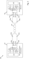
- Each transceiver 101, 102 comprises a pair of terminals 106a, 106b, 107a, 107b that connect to the transmission line 103 via respective capacitors 104a, 104b, 105a, 105b.
- a termination resistance Rterm 108, 109 is connected between the terminals of each transceiver 101, 102.
- Each transceiver 101, 102 comprises two receiver amplifiers RX 110a, 110b, 112a, 112b and one transmitter amplifier TX 111, 113 connected between the terminals 106a, 106b, 1071, 107b and a control module 114, 115.
- Figure 2 illustrates schematically the differential voltage between terminals TXP, TXN as a function of time at a transmitter during transmission of a logic level 1 followed by a logic level 0.
- the transmitter applies a positive differential voltage during a first phase over a first time period 201 followed by a negative differential voltage during a second phase over a second time period 202, and then followed by a zero differential voltage during a third phase over a third time period.
- the duration of the first and second time periods 201, 202 is approximately the same, while the duration of the third time period 203 is around twice that of each the first and second time periods.
- the transmitter first applies a negative differential voltage during a first phase, followed by a positive differential voltage in a second phase and a zero differential voltage in a third phase. Similar to that for a logic level 1, for the logic level 0 the third phase is around twice the length of each of the first and second phases.
- the differential voltage applied to the transmission line is made as high as possible.
- the power consumption of the transmitter mostly depends on the differential voltage applied and the bus load representing the equivalent resistance seen across the output connections TXP, TXN, which will include the termination resistance Rterm at the receiver side.
- the transmitter power consumption will increase if the termination resistance is connected at the transmitter side.
- the termination resistance may be disconnected during the first and second phases to save on power consumption by the transmitter.
- An example of a switchable termination resistance to reduce losses when transmitting a signal along the transmission line is disclosed in WO 88/03731 A1 , in which a termination resistor is switched into a transceiver circuit for a set length of time after a transmit/receive signal is enabled that is sufficient to receive the leading edge of a data bit over a transmission line.
- the design of a switchable termination resistance may be more complex due to the limited maximum acceptable gate voltage of MOSFETs, high electromagnetic interference and high common mode voltages.
- FIG. 3 An alternative communication system 300 is illustrated in Figure 3 , in which a switchable termination resistance is provided between the terminals 106a, 106b, 107a, 107b of each transceiver 101, 102 by connecting the termination resistance Rterm 303, 304 in series with a switch 301, 302, each switch 301, 302 being controllable by a respective one of the controllers 114, 115.
- the other components of the system 300 are otherwise similar to those in Figure 1 .
- the switch 301, 302 allows each transceiver to disconnect the termination resistance Rterm 303, 304 on the transmit side during the 1st and 2nd phases (see Figure 2 ), leading to half the power consumption for the same differential voltage due to the change of load upon disconnecting the resistance on the transmit side.
- a transmission line transceiver comprising:
- a communication system comprising:
- Each of the series connected resistors may have an equal resistance value.
- a resistance value of each of the series connected resistors may match a characteristic impedance of the transmission line.
- the characteristic impedance of the transmission line may be around 120 ⁇ +/- 15%.
- a resistance value of each of the series connected resistors may be greater than the resistance value of the termination resistance of each of the first and second transceivers. This allows the power consumption effect of the series connected resistors, which remain connected across the terminals, to be reduced.
- the resistance value of each of the series connected resistors may in some examples be between around 150 ⁇ and around 350 ⁇ .
- the capacitor may have a capacitance value of between around 10 nF and around 200 nF.
- the control module may be configured to transmit a data bit on the transmission line by:
- a third aspect there is provided a method of operating a transceiver according to the first aspect, the method comprising transmitting a data bit over the transmission line by:
- Each of the series connected resistors may have an equal resistance value.
- a resistance value of each of the series connected resistors may match a characteristic impedance of the transmission line.
- the characteristic impedance of the transmission line may be around 120 ⁇ +/- 15%.
- a resistance value of each of the series connected resistors may be greater than the resistance value of the termination resistance.
- the resistance value of each of the series connected resistors may be between around 150 ⁇ and around 350 ⁇ .
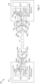
- Figure 4 illustrates a schematic diagram of an example communication system 400 comprising first and second transceivers 401, 402 connected by a transmission line 403, which in this example comprises a twisted wire pair.
- the transmission line 403 is isolated from the transceivers 401, 402 by isolation capacitors 404a, 404b, 405a, 405b at either end of the transmission line 403.
- the first transceiver 401 is in transmit mode and the second transceiver 402 is in receive mode.
- Each transceiver 401, 402 comprises a pair of terminals 406a, 406b, 407a, 407b that connect to the transmission line 403 via respective capacitors 404a, 404b, 405a, 405b.
- An internal termination resistance Rinternal 408, 409 is connected in series with a switch 410, 411 between the terminals 406a, 406b, 407a, 407b of each transceiver 401, 402.
- Each transceiver 401, 402 comprises two receiver amplifiers RX 412a, 412b, 413a, 413b and one transmitter amplifier TX 414, 415 connected between the terminals 406a, 406b, 407a, 407b and a control module 416, 417.
- a pair of series connected resistors Rsplit 418a, 418b, 419a, 419b is connected between the terminals 406a, 406b, 407a, 407b of each transceiver 401, 402.
- a capacitor Csplit 420, 421 is connected between a node 423, 424 connecting the pair of series connected resistors 418a, 418b, 419a, 419b and a common node 422.
- the series connected resistors 419a, 419b and the switchable termination resistor 409 provide a combined receiver load resistance Rload_RX for the transceiver operating as a receiver, which in this example is the second transceiver 402.
- the series connected resistors 418a, 418b, 419a, 419b and the capacitor 420, 421 are shown in Figure 4 as being external from the transceiver 401, 402. This is largely due to the value of the capacitor 420, 421 needing to be typically between around 10 and 200nF, which would result in a large IC area being taken up if the capacitor were to be internal to the transceiver.
- the switchable termination resistance circuit can, however, be internal to the transceiver 401, 402 because large capacitance values are not required. In a general aspect therefore, the switchable termination resistance circuit may be internal to the transceiver and the series connected resistors and capacitor external to the transceiver.
- the termination resistance Rinternal may be matched to the characteristic impedance of the transmission line 403 in order to avoid a reflection effect and rebound during communication.
- the characteristic impedance of an example cable for a transmission line 403 may be around 120 ⁇ .
- the split resistances Rsplit are indicated in Figure 4 as being connected external to each transceiver 401.
- the value for Rsplit may be selected that does not create misadaptation of the termination resistance, which results in the value for Rsplit being higher than the internal termination resistance Rinternal.
- the value for Rsplit maybe in the range 150-350 ⁇ with a termination resistance as indicated above.
- the total receiver load resistance Rload_RX should be around 130 ⁇ , resulting in a value for Rsplit being around 300 ⁇ .
- the equivalent resistive load is 102 ⁇ for the driver, which is the impedance seen by the driver during the 1st and 2nd phases when the internal termination resistance 409 is switched off..
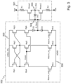
- FIG. 5 illustrates a schematic diagram of an example switchable termination resistance circuit 501 with an associated driving circuit 502.
- the switchable termination resistance circuit 501 is connected between first and second terminals TXP, TXN of a transceiver, such as either of the transceivers 101, 102 illustrated in Figure 4 .
- the switchable term ination resistance circuit 501 comprises first and second resistors R1, R2 connected to respective first and second terminals TXP, TXN.
- First and second NMOS termination resistance switches Mnsw1, Mnsw2 are connected in series between the first and second resistors R1, R2.
- Source connections of the termination resistance switches Mnsw1, Mnsw2 are connected together and drain connections of the termination resistance switches Mnsw1, Mnsw2 are connected to the respective first and second resistors R1, R2.
- Switching on the first and second termination resistance switches Mnsw1, Mnsw2 by applying a gate voltage to the gates of the termination resistance switches Mnsw1, Mnsw2 connects the first resistor R1 to the second resistor R2 via the first and second termination resistance switches Mnsw1, Mnsw2, thereby connecting a termination resistance between the first and second terminals TXP, TXN.
- the total termination resistance comprises the first and second resistors R1, R2 in series, together with the source-drain resistances of the first and second termination resistance switches Mnsw1, Mnsw2 (which may be a few Ohms). Switching off the first and second termination resistance switches Mnsw1, Mnsw2 disconnects the termination resistance from the first and second terminals TXP, TXN, leaving the connection between terminals TXP, TXN open circuit.
- Gate connections of the first and second termination resistance switches Mnsw1, Mnsw2 are connected to an input node 504, which is connected to an output of the driving circuit 502 for driving the switchable termination resistance circuit 501.
- Source connections of the first and second termination resistance switches Mnsw1, Mnsw2 are connected together at a midpoint node 503 of the switchable termination resistance circuit 501.
- a Zener diode Dz1 is connected between the input node 304 and the midpoint node 503, the cathode of the Zener diode Dz1 being connected to the input node 504.
- the Zener diode Dz1 maintains a gate-source voltage across the first and second termination resistance switches Mnsw1, Mnsw2 within a set voltage range defined by the breakdown voltage of the Zener diode.
- the Zener diode Dz1 thereby allows the switchable termination resistance circuit 501 to operate in the presence of electromagnetic interference, which may result in high voltages being induced across the first and second terminals TXP, TXN.
- the Zener diode may for example clamp the gate-source voltage across the termination resistance switches Mnsw1, Mnsw2 to 5V when the switchable terminal resistance circuit 501 is enabled.
- the common mode voltage on the transmission line connected to the first and second connections TXP, TXN may for example be around 2.5 V.
- a voltage at the input node 504 will need to be higher than around 5.5 V, but lower than the breakdown voltage of the Zener diode Dz1.
- the driving circuit 502 provides the gate voltage G_Nsw to the input node 504 that operates the first and second termination resistance switches Mnsw1, Mnsw2.
- the driving circuit 502 is connected between a supply voltage line 505 providing a supply voltage VPRE_TPL (for example 7V) and a ground voltage line 506 at a ground voltage AGND (for example 0V).
- the driving circuit 502 operates as a level shifter, allowing a low voltage input signal Rterm_en, Rterm_enb, to drive a higher voltage output signal G_Nsw, and allows the output voltage to float along with the voltage level at the midpoint node 503 of the switchable termination resistance circuit 501.
- the driving circuit 302 comprises first and second diodes D1, D2 connected to the input node 504, the first diode D1 having its cathode connected to the input node 304 and the second diode D2 having its anode connected to the input node 504. Diodes D1, D2 prevent current flowing back into the driving circuit 502 from the switchable termination resistance circuit 501 in the presence of high levels of electromagnetic interference.
- First, second and third NMOS switches Mn1, Mn2, Mn3 of the driving circuit 502 have source connections connected to the ground voltage line 505 and gate connections connected to receive a termination resistance enable signal Rterm_en or its inverse, Rterm_enb. Gate connections of the first and third NMOS switches Mn1, Mn3 receive Rterm_enb, while the second NMOS switch Mn2 receives Rterm_en.
- the driving circuit 502 further comprises first, second, third, fourth, fifth and sixth PMOS switches Mp1-Mp6.
- a gate connection of the first PMOS switch Mp1 is connected to a drain connection of the second PMOS switch Mp2.
- a gate connection of the second PMOS switch Mp2 is connected to a drain connection of the first PMOS switch Mp1.
- Source connections of the first, second and third PMOS switches are connected to the supply voltage line 504.
- a gate connection of the third PMOS switch Mp3 is connected to the drain connection of the second PMOS switch Mp2.
- a source connection of the fourth PMOS switch Mp4 is connected to the drain connection of the first PMOS switch Mp1 and a drain connection of the fourth PMOS switch Mp4 is connected to a drain connection of the first NMOS switch Mn1.
- a gate connection of the fourth PMOS switch Mp4 is connected to a gate connection of the fifth PMOS switch Mp5.
- a source connection of the fifth PMOS switch Mp5 is connected to the drain connection of the second PMOS switch Mp2.
- a drain connection of the fifth PMOS switch Mp5 is connected to a drain connection of the second NMOS switch Mn2.
- Gate connections of the fifth and sixth PMOS switches Mp5, Mp6 are connected together.
- a source connection of the sixth PMOS switch Mp6 is connected to a drain connection of the third PMOS switch Mp3.
- a drain connection of the sixth PMOS switch Mp6 is connected to an anode connection of the first diode D1.
- a drain connection of the third NMOS switch Mn3 is connected to the cathode connection of the second diode D2.
- the enable signal Rterm_en is provided to the second NMOS switch Mn2 and its inverse to the first and third NMOS switches Mn1, Mn3.
- the voltage applied at the input node 304 is then the supply voltage VPRE_TPL minus one diode voltage, i.e. the voltage across the first diode D1.
- the supply voltage VPRE_TPL needs to be sufficient to pull the gates of the termination switches Mnsw1, Mnsw2 but lower than that required to drive current through the Zener diode Dz1.
- the third NMOS switch Mn3 is turned on with Rterm_enb, which pulls down the drain of the NMOS switch Mn3 and the gate voltage at the input node 304 to one diode voltage about ground, thereby turning off the termination resistance switches Mnsw1, Mnsw2.
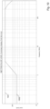
- a first plot 601 illustrates the common mode voltage as a function of frequency for a first communication system with only the switchable internal termination resistance.
- a second plot 602 illustrates the common mode voltage for a second communication system with the addition of the split resistance arrangement.
- the first communication system results in a peak common mode voltage of around 42V at around 7 MHz, while the second communication system has a substantially lower peak common mode voltage of around 20V around the same frequency.
- a value of 200 ⁇ was selected for Rsplit was a value of 100nF was selected for Csplit.
- the large effect of the split resistance arrangement can be seen particularly in the region of around 100kHz to around 10MHz.
- each of the nodes 1-6 represent a pair of transceivers as described herein, the nodes being controlled by a master TPL.
- Each of the nodes include two transceivers, for example node1 has a transceiver connected to the Master TPL and a second transceiver linked to node2. Also for example node3 has a first transceiver connected to node2 and a second transceiver of node3 is connected to node4 via a cable. BCI open loop levels were measured on transmission lines connecting each of the nodes.
- BCI was only injected on cables, for example on the cable between node3 and node4 at the position where the BCI probe is located.
- BCI may be injected on the cable between node1 and the Master TPL, which is not depicted in Figure 7 .
- Figure 8 shows plots of BCI open loop level (in mA) as a function of frequency (in MHz), compared to the limits defined by the VW TL81000 standard 801.
- a first plot 802 shows results using a switched termination resistance alone, which does not pass the standard due to falling below the required level between around 5-7 MHz.
- a second plot 803 shows results using a switched termination resistance in combination with a split resistor arrangement, with the values for Rsplit and Csplitof 200 ⁇ and 100nF respectively, which passes the standard over the entire frequency range.
- the level of injection is increased from around 100/150mA to around 200mA, leading to a higher immunity to noise below 2MHz. Further optimization by selection of values for the split resistances and capacitance may result in better performance.
- Figure 9 illustrates a plot 901 of BCI open loop level as a function of frequency for a communications system with only an internal switchable termination resistance, i.e. similar to the arrangement in Figure 3 , compared to the TL81000 standard 902 and with the more stringent ISO 11452-4 Level 4 standard 903. This shows that, while meeting the TL81000 standard, the BCI level fails the more stringent standard 903 over the range of between around 1 and 6 MHz, which is due to a high common mode within this frequency range.
- Figure 10 illustrates a plot 1001 of BCI open loop level as a function of frequency for a communications system with the addition of a split resistance arrangement, i.e. similar to the arrangement of Figure 4 , again compared to the ISO 11452-4 Level 4 standard 1002. This shows that, with proper optimization of the components, the split resistance arrangement solution allows the system to pass a 200mA BCI level over the full range of frequency. This was applied in two setups tested on a distributed system. The same setup was tested on a centralized board with similar results.
- the split resistance arrangement described herein allows for a substantial improved in EMC robustness during BCI tests with for example only an increase of around 20% in power consumption during transmission compared to arrangements with an internal switchable termination resistance alone.
- the solution demonstrates a power consumption around 40% lower than conventional arrangements with only an external termination resistance.
- the transmission system described herein may be particularly applicable in battery management systems, for example for vehicle battery systems, in which isolated electrical communication is required, current consumption is a critical parameter and electromagnetic interference may be high.
- the transmission system described herein may also be applicable in other applications where isolated transmission with a low current consumption, particularly in the presence of high electromagnetic interference, may be required.
Landscapes
- Engineering & Computer Science (AREA)
- Computer Networks & Wireless Communication (AREA)
- Signal Processing (AREA)
- Power Engineering (AREA)
- Dc Digital Transmission (AREA)
Abstract
The disclosure relates to a transceiver physical layer interface. Example embodiments include a transmission line transceiver (401) comprising: first and second terminals (406a, 406b); a control module (416); an amplifier module (414) connected between the control module (416) and the first and second terminals (406a, 406b); a switchable termination resistance circuit (408, 410) connected between the first and second terminals (406a, 406b), the switchable termination resistance circuit (408, 410) comprising a termination resistance (408) connected in series with a switch (410) controllable by the control module (416); a pair of series connected resistors (418a, 418b) connected between the first and second terminals (406a, 406b); a capacitor (420) connected between a node (423) connecting the pair of series connected resistors (418a, 418b) and a common node (422), wherein the control module (416) is configured to open the switch (410) to disconnect the termination resistance (408) during transmission of a signal via a transmission line (403) capacitively connected to the first and second terminals (406a, 406b).
Description
- The disclosure relates to a transceiver physical layer interface.
- In a communication system comprising a pair of transceivers passing signals along a transmission line, a termination resistance at each transceiver serves to reduce reflections along the transmission line.
- An example of a communication system comprising a pair of transceivers connected by a transmission line is illustrated in
Figure 1 . Thesystem 100 comprises first andsecond transceivers transmission line 103, which in this example comprises a twisted wire pair. Eachtransceiver transmission line 103 is isolated from thetransceivers isolation capacitors transmission line 103. In the illustrated example, thefirst transceiver 101 is in transmit mode and thesecond transceiver 102 is in receive mode. Eachtransceiver terminals transmission line 103 viarespective capacitors transceiver transceiver receiver amplifiers RX transmitter amplifier TX terminals control module -
Figure 2 illustrates schematically the differential voltage between terminals TXP, TXN as a function of time at a transmitter during transmission of alogic level 1 followed by alogic level 0. For alogic level 1, the transmitter applies a positive differential voltage during a first phase over afirst time period 201 followed by a negative differential voltage during a second phase over asecond time period 202, and then followed by a zero differential voltage during a third phase over a third time period. The duration of the first andsecond time periods third time period 203 is around twice that of each the first and second time periods. For alogic level 0, the transmitter first applies a negative differential voltage during a first phase, followed by a positive differential voltage in a second phase and a zero differential voltage in a third phase. Similar to that for alogic level 1, for thelogic level 0 the third phase is around twice the length of each of the first and second phases. - To mitigate line attenuation, the differential voltage applied to the transmission line is made as high as possible. The power consumption of the transmitter mostly depends on the differential voltage applied and the bus load representing the equivalent resistance seen across the output connections TXP, TXN, which will include the termination resistance Rterm at the receiver side.
- During the first and second phases, the transmitter power consumption will increase if the termination resistance is connected at the transmitter side. To reduce this, the termination resistance may be disconnected during the first and second phases to save on power consumption by the transmitter. An example of a switchable termination resistance to reduce losses when transmitting a signal along the transmission line is disclosed in
WO 88/03731 A1 - For line transmission systems where operation at high voltages under electromagnetic interference is required, for example in automotive applications, the design of a switchable termination resistance may be more complex due to the limited maximum acceptable gate voltage of MOSFETs, high electromagnetic interference and high common mode voltages.
- An
alternative communication system 300 is illustrated inFigure 3 , in which a switchable termination resistance is provided between theterminals transceiver termination resistance Rterm switch switch controllers system 300 are otherwise similar to those inFigure 1 . Theswitch termination resistance Rterm Figure 2 ), leading to half the power consumption for the same differential voltage due to the change of load upon disconnecting the resistance on the transmit side. This solution optimises power consumption but a disadvantage is that this results in a high induced common mode voltage when subjected to bulk current injection (BCI) interference. Although the solution works for transformer coupled transmission lines, a switched termination resistance is not an ideal solution in combination with a capacitively coupled transmission line. - According to a first aspect there is provided a transmission line transceiver comprising:
- first and second terminals;
- a control module;
- an amplifier module connected between the control module and the first and second terminals;
- a switchable termination resistance circuit connected between the first and second terminals, the switchable termination resistance circuit comprising a termination resistance connected in series with a switch controllable by the control module;
- a pair of series connected resistors connected between the first and second terminals;
- a capacitor connected between a node connecting the pair of series connected resistors and a common node,
- wherein the control module is configured to operate the switch to disconnect the termination resistance during transmission of a signal via a transmission line capacitively connected to the first and second terminals.
- According to a second aspect there is provided a communication system comprising:
- first and second transceivers, each of the first and second transceivers according to the first aspect; and
- a transmission line connected to the first and second terminals of each of the first and second transceivers via isolation capacitors.
- Each of the series connected resistors may have an equal resistance value.
- A resistance value of each of the series connected resistors may match a characteristic impedance of the transmission line.
- The characteristic impedance of the transmission line may be around 120Ω +/- 15%.
- A resistance value of each of the series connected resistors may be greater than the resistance value of the termination resistance of each of the first and second transceivers. This allows the power consumption effect of the series connected resistors, which remain connected across the terminals, to be reduced.
- The resistance value of each of the series connected resistors may in some examples be between around 150Ω and around 350Ω.
- The capacitor may have a capacitance value of between around 10 nF and around 200 nF.
- The control module may be configured to transmit a data bit on the transmission line by:
- providing first and second pulses to the amplifier module to drive respective positive and negative differential voltage levels across the first and second terminals during respective first and second time periods while maintaining the switch open; and
- maintaining the switch closed during a subsequent third time period.
- According to a third aspect there is provided a method of operating a transceiver according to the first aspect, the method comprising transmitting a data bit over the transmission line by:
- the control module providing first and second pulses to the amplifier module to drive respective positive and negative differential voltage levels across the first and second terminals during respective first and second time periods; and
- the control module maintaining the switch closed during a subsequent third time period.
- Each of the series connected resistors may have an equal resistance value.
- A resistance value of each of the series connected resistors may match a characteristic impedance of the transmission line.
- The characteristic impedance of the transmission line may be around 120Ω +/- 15%.
- A resistance value of each of the series connected resistors may be greater than the resistance value of the termination resistance.
- The resistance value of each of the series connected resistors may be between around 150Ω and around 350Ω.
- Embodiments will be described, by way of example only, with reference to the drawings, in which:
-
Figure 1 is a schematic diagram of a communication system comprising a pair of transceivers connected with a capacitively coupled transmission line; -
Figure 2 illustrates a schematic illustration of differential voltage on a transmission line as a function of time; -
Figure 3 is a schematic diagram of an alternative communication system comprising a pair of transceivers connected with a capacitively transmission line; -
Figure 4 is a schematic diagram of a further communication system comprising a pair of transceivers connected with a capacitively coupled transmission line with a split filter connected to each transceiver; -
Figure 5 is a schematic diagram of a switchable termination resistance circuit and associated driving circuit for a transmission line communication system; -
Figure 6 is a plot of common mode voltage as a function of frequency for two different capacitively coupled transmission line communication systems; -
Figure 7 is a schematic diagram of an experimental setup for testing of bulk current injection interference on a transmission line; -
Figure 8 is a plot of BCI open loop level as a function of frequency for a communication system with and without a split filter; -
Figure 9 is a plot of BCI open loop level as a function of frequency for a communication system with a switched termination resistance; -
Figure 10 is a further plot of BCI open loop level as a function of frequency for a communication system with a switched termination resistance with a split filter. - It should be noted that the Figures are diagrammatic and not drawn to scale. Relative dimensions and proportions of parts of these Figures may be shown exaggerated or reduced in size, for the sake of clarity and convenience in the drawings. The same reference signs are generally used to refer to corresponding or similar feature in modified and different embodiments.
-
Figure 4 illustrates a schematic diagram of anexample communication system 400 comprising first andsecond transceivers transmission line 403, which in this example comprises a twisted wire pair. As with the communication system ofFigure 1 , thetransmission line 403 is isolated from thetransceivers isolation capacitors transmission line 403. In the illustrated example, thefirst transceiver 401 is in transmit mode and thesecond transceiver 402 is in receive mode. Eachtransceiver terminals transmission line 403 viarespective capacitors termination resistance Rinternal switch terminals transceiver transceiver receiver amplifiers RX transmitter amplifier TX terminals control module - A pair of series connected
resistors Rsplit terminals transceiver capacitor Csplit node resistors common node 422. The series connectedresistors switchable termination resistor 409 provide a combined receiver load resistance Rload_RX for the transceiver operating as a receiver, which in this example is thesecond transceiver 402. - The series connected
resistors capacitor Figure 4 as being external from thetransceiver capacitor transceiver - The termination resistance Rinternal may be matched to the characteristic impedance of the
transmission line 403 in order to avoid a reflection effect and rebound during communication. The characteristic impedance of an example cable for atransmission line 403 may be around 120Ω. - The split resistances Rsplit are indicated in
Figure 4 as being connected external to eachtransceiver 401. The value for Rsplit may be selected that does not create misadaptation of the termination resistance, which results in the value for Rsplit being higher than the internal termination resistance Rinternal. Typically, the value for Rsplit maybe in the range 150-350Ω with a termination resistance as indicated above. - In a specific example, if the internal termination resistance value is set to 170Ω, in order to use as low as possible Rsplit with the same differential voltage generated, the total receiver load resistance Rload_RX should be around 130Ω, resulting in a value for Rsplit being around 300Ω.
- With Rsplit=250Ω and Rinternal=170Ω, the receiver load resistance is Rload_RX=127Ω. The equivalent resistive load is 102Ω for the driver, which is the impedance seen by the driver during the 1st and 2nd phases when the
internal termination resistance 409 is switched off.. - With Rsplit=200Ω and Rinternal=170Ω, the receiver load resistance Rload_RX=119Ω and the equivalent resistive load is 92Ω.
- With Rsplit=150Ω and Rinternal=170Ω, the receiver load resistance Rload_RX=109Ω and the equivalent resistive load is 80Ω.
-
Figure 5 illustrates a schematic diagram of an example switchabletermination resistance circuit 501 with an associated drivingcircuit 502. The switchabletermination resistance circuit 501 is connected between first and second terminals TXP, TXN of a transceiver, such as either of thetransceivers Figure 4 . The switchable termination resistance circuit 501 comprises first and second resistors R1, R2 connected to respective first and second terminals TXP, TXN. First and second NMOS termination resistance switches Mnsw1, Mnsw2 are connected in series between the first and second resistors R1, R2. Source connections of the termination resistance switches Mnsw1, Mnsw2 are connected together and drain connections of the termination resistance switches Mnsw1, Mnsw2 are connected to the respective first and second resistors R1, R2. Switching on the first and second termination resistance switches Mnsw1, Mnsw2 by applying a gate voltage to the gates of the termination resistance switches Mnsw1, Mnsw2 connects the first resistor R1 to the second resistor R2 via the first and second termination resistance switches Mnsw1, Mnsw2, thereby connecting a termination resistance between the first and second terminals TXP, TXN. The total termination resistance comprises the first and second resistors R1, R2 in series, together with the source-drain resistances of the first and second termination resistance switches Mnsw1, Mnsw2 (which may be a few Ohms). Switching off the first and second termination resistance switches Mnsw1, Mnsw2 disconnects the termination resistance from the first and second terminals TXP, TXN, leaving the connection between terminals TXP, TXN open circuit. - Gate connections of the first and second termination resistance switches Mnsw1, Mnsw2 are connected to an
input node 504, which is connected to an output of the drivingcircuit 502 for driving the switchabletermination resistance circuit 501. Source connections of the first and second termination resistance switches Mnsw1, Mnsw2 are connected together at amidpoint node 503 of the switchabletermination resistance circuit 501. A Zener diode Dz1 is connected between theinput node 304 and themidpoint node 503, the cathode of the Zener diode Dz1 being connected to theinput node 504. The Zener diode Dz1 maintains a gate-source voltage across the first and second termination resistance switches Mnsw1, Mnsw2 within a set voltage range defined by the breakdown voltage of the Zener diode. The Zener diode Dz1 thereby allows the switchabletermination resistance circuit 501 to operate in the presence of electromagnetic interference, which may result in high voltages being induced across the first and second terminals TXP, TXN. The Zener diode may for example clamp the gate-source voltage across the termination resistance switches Mnsw1, Mnsw2 to 5V when the switchableterminal resistance circuit 501 is enabled. - During normal operation in the absence of electromagnetic interference, the common mode voltage on the transmission line connected to the first and second connections TXP, TXN may for example be around 2.5 V. To operate the switches Mnsw1, Mnsw2 a voltage at the
input node 504 will need to be higher than around 5.5 V, but lower than the breakdown voltage of the Zener diode Dz1. - The driving
circuit 502 provides the gate voltage G_Nsw to theinput node 504 that operates the first and second termination resistance switches Mnsw1, Mnsw2. The drivingcircuit 502 is connected between asupply voltage line 505 providing a supply voltage VPRE_TPL (for example 7V) and aground voltage line 506 at a ground voltage AGND (for example 0V). - The driving
circuit 502 operates as a level shifter, allowing a low voltage input signal Rterm_en, Rterm_enb, to drive a higher voltage output signal G_Nsw, and allows the output voltage to float along with the voltage level at themidpoint node 503 of the switchabletermination resistance circuit 501. To allow the output voltage to float, the drivingcircuit 302 comprises first and second diodes D1, D2 connected to theinput node 504, the first diode D1 having its cathode connected to theinput node 304 and the second diode D2 having its anode connected to theinput node 504. Diodes D1, D2 prevent current flowing back into the drivingcircuit 502 from the switchabletermination resistance circuit 501 in the presence of high levels of electromagnetic interference. - First, second and third NMOS switches Mn1, Mn2, Mn3 of the driving
circuit 502 have source connections connected to theground voltage line 505 and gate connections connected to receive a termination resistance enable signal Rterm_en or its inverse, Rterm_enb. Gate connections of the first and third NMOS switches Mn1, Mn3 receive Rterm_enb, while the second NMOS switch Mn2 receives Rterm_en. - The driving
circuit 502 further comprises first, second, third, fourth, fifth and sixth PMOS switches Mp1-Mp6. A gate connection of the first PMOS switch Mp1 is connected to a drain connection of the second PMOS switch Mp2. A gate connection of the second PMOS switch Mp2 is connected to a drain connection of the first PMOS switch Mp1. Source connections of the first, second and third PMOS switches are connected to thesupply voltage line 504. A gate connection of the third PMOS switch Mp3 is connected to the drain connection of the second PMOS switch Mp2. - A source connection of the fourth PMOS switch Mp4 is connected to the drain connection of the first PMOS switch Mp1 and a drain connection of the fourth PMOS switch Mp4 is connected to a drain connection of the first NMOS switch Mn1. A gate connection of the fourth PMOS switch Mp4 is connected to a gate connection of the fifth PMOS switch Mp5. A source connection of the fifth PMOS switch Mp5 is connected to the drain connection of the second PMOS switch Mp2. A drain connection of the fifth PMOS switch Mp5 is connected to a drain connection of the second NMOS switch Mn2.
- Gate connections of the fifth and sixth PMOS switches Mp5, Mp6 are connected together. A source connection of the sixth PMOS switch Mp6 is connected to a drain connection of the third PMOS switch Mp3. A drain connection of the sixth PMOS switch Mp6 is connected to an anode connection of the first diode D1.
- A drain connection of the third NMOS switch Mn3 is connected to the cathode connection of the second diode D2.
- To turn on the termination resistance, the enable signal Rterm_en is provided to the second NMOS switch Mn2 and its inverse to the first and third NMOS switches Mn1, Mn3. The voltage applied at the
input node 304 is then the supply voltage VPRE_TPL minus one diode voltage, i.e. the voltage across the first diode D1. The supply voltage VPRE_TPL needs to be sufficient to pull the gates of the termination switches Mnsw1, Mnsw2 but lower than that required to drive current through the Zener diode Dz1. - To turn off the termination resistance, the third NMOS switch Mn3 is turned on with Rterm_enb, which pulls down the drain of the NMOS switch Mn3 and the gate voltage at the
input node 304 to one diode voltage about ground, thereby turning off the termination resistance switches Mnsw1, Mnsw2. - In simulation, the difference in common mode voltage was evaluated for a communications system with the split resistance arrangement of
Figure 4 compared to a system with only a switchable internal termination resistance. The results of this simulation are illustrated inFigure 6 . Afirst plot 601 illustrates the common mode voltage as a function of frequency for a first communication system with only the switchable internal termination resistance. Asecond plot 602 illustrates the common mode voltage for a second communication system with the addition of the split resistance arrangement. The first communication system results in a peak common mode voltage of around 42V at around 7 MHz, while the second communication system has a substantially lower peak common mode voltage of around 20V around the same frequency. In these simulated results, a value of 200Ω was selected for Rsplit was a value of 100nF was selected for Csplit. The large effect of the split resistance arrangement can be seen particularly in the region of around 100kHz to around 10MHz. - The arrangements were tested on silicon in BCI measurements using the experimental setup illustrated in
Figure 7 , in which each of the nodes 1-6 represent a pair of transceivers as described herein, the nodes being controlled by a master TPL. Each of the nodes include two transceivers, for example node1 has a transceiver connected to the Master TPL and a second transceiver linked to node2. Also for example node3 has a first transceiver connected to node2 and a second transceiver of node3 is connected to node4 via a cable. BCI open loop levels were measured on transmission lines connecting each of the nodes. In the experimental setup, BCI was only injected on cables, for example on the cable between node3 and node4 at the position where the BCI probe is located. In alternative setups BCI may be injected on the cable between node1 and the Master TPL, which is not depicted inFigure 7 . - The results of the experimental arrangement are illustrated in
Figure 8 , which shows plots of BCI open loop level (in mA) as a function of frequency (in MHz), compared to the limits defined by the VW TL81000 standard 801. Afirst plot 802 shows results using a switched termination resistance alone, which does not pass the standard due to falling below the required level between around 5-7 MHz. Asecond plot 803 shows results using a switched termination resistance in combination with a split resistor arrangement, with the values for Rsplit and Csplitof 200Ω and 100nF respectively, which passes the standard over the entire frequency range. Moreover, at low frequencies the level of injection is increased from around 100/150mA to around 200mA, leading to a higher immunity to noise below 2MHz. Further optimization by selection of values for the split resistances and capacitance may result in better performance. -
Figure 9 illustrates aplot 901 of BCI open loop level as a function of frequency for a communications system with only an internal switchable termination resistance, i.e. similar to the arrangement inFigure 3 , compared to the TL81000 standard 902 and with the more stringent ISO 11452-4 Level 4standard 903. This shows that, while meeting the TL81000 standard, the BCI level fails the more stringent standard 903 over the range of between around 1 and 6 MHz, which is due to a high common mode within this frequency range. -
Figure 10 illustrates aplot 1001 of BCI open loop level as a function of frequency for a communications system with the addition of a split resistance arrangement, i.e. similar to the arrangement ofFigure 4 , again compared to the ISO 11452-4 Level 4 standard 1002. This shows that, with proper optimization of the components, the split resistance arrangement solution allows the system to pass a 200mA BCI level over the full range of frequency. This was applied in two setups tested on a distributed system. The same setup was tested on a centralized board with similar results. - In summary, the split resistance arrangement described herein allows for a substantial improved in EMC robustness during BCI tests with for example only an increase of around 20% in power consumption during transmission compared to arrangements with an internal switchable termination resistance alone. The solution demonstrates a power consumption around 40% lower than conventional arrangements with only an external termination resistance.
- The transmission system described herein may be particularly applicable in battery management systems, for example for vehicle battery systems, in which isolated electrical communication is required, current consumption is a critical parameter and electromagnetic interference may be high. The transmission system described herein may also be applicable in other applications where isolated transmission with a low current consumption, particularly in the presence of high electromagnetic interference, may be required.
- From reading the present disclosure, other variations and modifications will be apparent to the skilled person. Such variations and modifications may involve equivalent and other features which are already known in the art of transmission line transceivers, and which may be used instead of, or in addition to, features already described herein.
- Although the appended claims are directed to particular combinations of features, it should be understood that the scope of the disclosure of the present invention also includes any novel feature or any novel combination of features disclosed herein either explicitly or implicitly or any generalisation thereof, whether or not it relates to the same invention as presently claimed in any claim and whether or not it mitigates any or all of the same technical problems as does the present invention.
- Features which are described in the context of separate embodiments may also be provided in combination in a single embodiment. Conversely, various features which are, for brevity, described in the context of a single embodiment, may also be provided separately or in any suitable sub-combination. The applicant hereby gives notice that new claims may be formulated to such features and/or combinations of such features during the prosecution of the present application or of any further application derived therefrom.
- For the sake of completeness it is also stated that the term "comprising" does not exclude other elements or steps, the term "a" or "an" does not exclude a plurality, a single processor or other unit may fulfil the functions of several means recited in the claims and reference signs in the claims shall not be construed as limiting the scope of the claims.
Claims (15)
- A transmission line transceiver (401) comprising:first and second terminals (406a, 406b);a control module (416);an amplifier module (414) connected between the control module (416) and the first and second terminals (406a, 406b);a switchable termination resistance circuit (408, 410) connected between the first and second terminals (406a, 406b), the switchable termination resistance circuit (408, 410) comprising a termination resistance (408) connected in series with a switch (410) controllable by the control module (416);a pair of series connected resistors (418a, 418b) connected between the first and second terminals (406a, 406b);a capacitor (420) connected between a node (423) connecting the pair of series connected resistors (418a, 418b) and a common node (422),wherein the control module (416) is configured to operate the switch (410) to disconnect the termination resistance (408) during transmission of a signal via a transmission line (403) capacitively connected to the first and second terminals (406a, 406b).
- A communication system (400) comprising:first and second transceivers (401, 402), each of the first and second transceivers (401, 402) according to claim 1; anda transmission line (403) connected to the first and second terminals (407a, 407b, 406a, 406b) of each of the first and second transceivers (401, 402) via isolation capacitors (405a, 405b, 404a, 404b).
- The communication system (400) of claim 2, wherein each of the series connected resistors (419a, 419b, 418a, 418b) has an equal resistance value.
- The communication system (400) of claim 2, wherein a resistance value of each of the series connected resistors (419a, 419b, 418a, 418b) matches a characteristic impedance of the transmission line (403).
- The communication system (400) of claim 3, wherein the characteristic impedance of the transmission line (403) is around 120Ω +/- 15%.
- The communication system (400) of claim 3 or claim 4, wherein a resistance value of each of the series connected resistors (419a, 419b, 418a, 418b) is greater than the resistance value of the termination resistance (409, 408) of each of the first and second transceivers (401, 402).
- The transmission line transceiver (402) or communication system (400) of any preceding claim, wherein the resistance value of each of the series connected resistors (419a, 419b, 418a, 418b) is between around 150Ω and around 350Ω.
- The transmission line transceiver (402) or communication system (400) of any preceding claim, wherein the capacitor (420, 421) has a capacitance value of between around 10 nF and around 200 nF.
- The transmission line transceiver (402) or communication system (400) of any preceding claim, wherein the control module (416) is configured to transmit a data bit on the transmission line (403) by:providing first and second pulses to the amplifier module (414) to drive respective positive and negative differential voltage levels across the first and second terminals (406a, 406b) during respective first and second time periods (201, 202) while maintaining the switch (410) open; andmaintaining the switch (410) closed during a subsequent third time period (203).
- A method of operating a transceiver according to claim 1, the method comprising transmitting a data bit over the transmission line (403) by:the control module (416) providing first and second pulses to the amplifier module (414) to drive respective positive and negative differential voltage levels across the first and second terminals (406a, 406b) during respective first and second time periods (201, 202); andthe control module (416) maintaining the switch (410) closed during a subsequent third time period (203).
- The method of claim 10, wherein each of the series connected resistors (419a, 419b, 418a, 418b) has an equal resistance value.
- The method of claim 10, wherein a resistance value of each of the series connected resistors (418a, 418b) matches a characteristic impedance of the transmission line (403).
- The method of claim 12, wherein the characteristic impedance of the transmission line (403) is around 120Ω +/- 15%.
- The method of claim 12 or claim 13, wherein a resistance value of each of the series connected resistors (418a, 418b) is greater than the resistance value of the termination resistance (408).
- The method of any one of claims 10 to 14, wherein the resistance value of each of the series connected resistors (418a, 418b) is between around 150Ω and around 350Ω.
Priority Applications (3)
| Application Number | Priority Date | Filing Date | Title |
|---|---|---|---|
| EP23306593.7A EP4529024A1 (en) | 2023-09-25 | 2023-09-25 | Transceiver physical layer interface |
| CN202411150383.0A CN119696618A (en) | 2023-09-25 | 2024-08-21 | Transceiver physical layer interface |
| US18/882,046 US12494952B2 (en) | 2023-09-25 | 2024-09-11 | Transceiver physical layer interface |
Applications Claiming Priority (1)
| Application Number | Priority Date | Filing Date | Title |
|---|---|---|---|
| EP23306593.7A EP4529024A1 (en) | 2023-09-25 | 2023-09-25 | Transceiver physical layer interface |
Publications (1)
| Publication Number | Publication Date |
|---|---|
| EP4529024A1 true EP4529024A1 (en) | 2025-03-26 |
Family
ID=88315833
Family Applications (1)
| Application Number | Title | Priority Date | Filing Date |
|---|---|---|---|
| EP23306593.7A Pending EP4529024A1 (en) | 2023-09-25 | 2023-09-25 | Transceiver physical layer interface |
Country Status (3)
| Country | Link |
|---|---|
| US (1) | US12494952B2 (en) |
| EP (1) | EP4529024A1 (en) |
| CN (1) | CN119696618A (en) |
Cited By (1)
| Publication number | Priority date | Publication date | Assignee | Title |
|---|---|---|---|---|
| US20250253649A1 (en) * | 2024-02-06 | 2025-08-07 | Rockwell Automation Technologies, Inc. | Circuit to improve ethernet immunity to electrical fast transient |
Citations (3)
| Publication number | Priority date | Publication date | Assignee | Title |
|---|---|---|---|---|
| WO1988003731A1 (en) | 1986-11-10 | 1988-05-19 | Ncr Corporation | Terminator for a transceiver device |
| US20140256276A1 (en) * | 2013-03-05 | 2014-09-11 | Qualcomm Incorporated | Unified front-end receiver interface for accommodating incoming signals via ac-coupling or dc-coupling |
| EP3745662A1 (en) * | 2018-01-23 | 2020-12-02 | Sony Semiconductor Solutions Corporation | Communication system and communication method |
Family Cites Families (12)
| Publication number | Priority date | Publication date | Assignee | Title |
|---|---|---|---|---|
| JPH1020974A (en) | 1996-07-03 | 1998-01-23 | Fujitsu Ltd | Bus structure and input / output buffer |
| US6078204A (en) | 1996-12-19 | 2000-06-20 | Texas Instruments Incorporated | High current drain-to-gate clamp/gate-to-source clamp for external power MOS transistors |
| WO1998051046A1 (en) | 1997-05-07 | 1998-11-12 | California Micro Devices Corporation | Active termination circuit and method therefor |
| US6590413B1 (en) | 2001-10-03 | 2003-07-08 | Altera Corporation | Self-tracking integrated differential termination resistance |
| CN100481693C (en) | 2006-03-10 | 2009-04-22 | 昂宝电子(上海)有限公司 | System and method for electrification reset and under-voltage locking scheme |
| JP2012249236A (en) * | 2011-05-31 | 2012-12-13 | Renesas Mobile Corp | Semiconductor integrated circuit device, electronic device, and radio communication terminal |
| JP6298629B2 (en) | 2013-12-24 | 2018-03-20 | 株式会社メガチップス | Data receiver |
| DE102015204606A1 (en) * | 2015-03-13 | 2016-09-15 | Robert Bosch Gmbh | Transmitting and receiving circuit for transmitting differential and single-ended signals via transmission lines |
| DE102015121732B4 (en) | 2015-12-14 | 2022-07-14 | Knorr-Bremse Systeme für Nutzfahrzeuge GmbH | Circuit arrangement for a switchable line termination of a serial bus |
| CN212183126U (en) | 2020-05-28 | 2020-12-18 | 深圳市泛仕达科技有限公司 | Reverse connection prevention protection circuit with soft start |
| EP4270886B1 (en) | 2022-04-29 | 2026-03-18 | NXP USA, Inc. | Switchable termination resistance circuit |
| EP4270885B1 (en) | 2022-04-29 | 2026-03-04 | NXP USA, Inc. | Switchable termination resistance circuit |
-
2023
- 2023-09-25 EP EP23306593.7A patent/EP4529024A1/en active Pending
-
2024
- 2024-08-21 CN CN202411150383.0A patent/CN119696618A/en active Pending
- 2024-09-11 US US18/882,046 patent/US12494952B2/en active Active
Patent Citations (3)
| Publication number | Priority date | Publication date | Assignee | Title |
|---|---|---|---|---|
| WO1988003731A1 (en) | 1986-11-10 | 1988-05-19 | Ncr Corporation | Terminator for a transceiver device |
| US20140256276A1 (en) * | 2013-03-05 | 2014-09-11 | Qualcomm Incorporated | Unified front-end receiver interface for accommodating incoming signals via ac-coupling or dc-coupling |
| EP3745662A1 (en) * | 2018-01-23 | 2020-12-02 | Sony Semiconductor Solutions Corporation | Communication system and communication method |
Cited By (1)
| Publication number | Priority date | Publication date | Assignee | Title |
|---|---|---|---|---|
| US20250253649A1 (en) * | 2024-02-06 | 2025-08-07 | Rockwell Automation Technologies, Inc. | Circuit to improve ethernet immunity to electrical fast transient |
Also Published As
| Publication number | Publication date |
|---|---|
| US20250106072A1 (en) | 2025-03-27 |
| US12494952B2 (en) | 2025-12-09 |
| CN119696618A (en) | 2025-03-25 |
Similar Documents
| Publication | Publication Date | Title |
|---|---|---|
| JP2722213B2 (en) | Matching device | |
| EP0777311B1 (en) | Combined data and power transmission | |
| CN106464558B (en) | Subscriber station for a bus system and method for increasing the noise immunity in the range of the electromagnetic compatibility of a subscriber station | |
| CN109714234B (en) | Transceiver unit for transmitting data via a differential bus | |
| US8027377B2 (en) | Differential driver with common-mode voltage tracking and method | |
| CN100390558C (en) | Input and output circuits and test equipment | |
| EP4346110A1 (en) | A transmitter circuit | |
| US12494952B2 (en) | Transceiver physical layer interface | |
| US20230353142A1 (en) | Switchable termination resistance circuit | |
| US9780744B2 (en) | Transceiver circuit for communicating differential and single-ended signals via transmission lines | |
| US8823421B2 (en) | Pre-emphasis circuit | |
| CN111837364A (en) | Transmit/receive device for bus system and method for reducing wired emissions | |
| CN111837365A (en) | Transmit/receive device for bus system and method for reducing wired emissions | |
| EP2315402A1 (en) | Automatic de-emphasis setting for driving capacitive backplane | |
| US12231105B2 (en) | Switchable termination resistance circuit | |
| US12047104B2 (en) | Communications system | |
| CN216819835U (en) | Single-wire isolated communication device and system | |
| US12081371B2 (en) | Device for can transceiver, transceiver and method | |
| US12542539B2 (en) | Switchable termination resistance circuit | |
| CN117478211A (en) | Burst transmission signal conditioning circuit, method, device, chip and electronic equipment | |
| US8305099B2 (en) | High speed full duplex test interface | |
| US7218892B2 (en) | Passive repeater/terminator | |
| CN115800955A (en) | Impedance matching circuit, field bus board card and impedance matching method | |
| CN117478124A (en) | Bidirectional digital isolator and communication method | |
| US7948275B2 (en) | Transceiver with fault tolerant driver |
Legal Events
| Date | Code | Title | Description |
|---|---|---|---|
| PUAI | Public reference made under article 153(3) epc to a published international application that has entered the european phase |
Free format text: ORIGINAL CODE: 0009012 |
|
| STAA | Information on the status of an ep patent application or granted ep patent |
Free format text: STATUS: THE APPLICATION HAS BEEN PUBLISHED |
|
| AK | Designated contracting states |
Kind code of ref document: A1 Designated state(s): AL AT BE BG CH CY CZ DE DK EE ES FI FR GB GR HR HU IE IS IT LI LT LU LV MC ME MK MT NL NO PL PT RO RS SE SI SK SM TR |
|
| STAA | Information on the status of an ep patent application or granted ep patent |
Free format text: STATUS: REQUEST FOR EXAMINATION WAS MADE |
|
| 17P | Request for examination filed |
Effective date: 20250926 |