EP4528936A1 - Connector and electronic device - Google Patents
Connector and electronic device Download PDFInfo
- Publication number
- EP4528936A1 EP4528936A1 EP23807478.5A EP23807478A EP4528936A1 EP 4528936 A1 EP4528936 A1 EP 4528936A1 EP 23807478 A EP23807478 A EP 23807478A EP 4528936 A1 EP4528936 A1 EP 4528936A1
- Authority
- EP
- European Patent Office
- Prior art keywords
- insulator
- contact
- extending
- connector
- curved
- Prior art date
- Legal status (The legal status is an assumption and is not a legal conclusion. Google has not performed a legal analysis and makes no representation as to the accuracy of the status listed.)
- Pending
Links
Images






Classifications
-
- H—ELECTRICITY
- H01—ELECTRIC ELEMENTS
- H01R—ELECTRICALLY-CONDUCTIVE CONNECTIONS; STRUCTURAL ASSOCIATIONS OF A PLURALITY OF MUTUALLY-INSULATED ELECTRICAL CONNECTING ELEMENTS; COUPLING DEVICES; CURRENT COLLECTORS
- H01R12/00—Structural associations of a plurality of mutually-insulated electrical connecting elements, specially adapted for printed circuits, e.g. printed circuit boards [PCB], flat or ribbon cables, or like generally planar structures, e.g. terminal strips, terminal blocks; Coupling devices specially adapted for printed circuits, flat or ribbon cables, or like generally planar structures; Terminals specially adapted for contact with, or insertion into, printed circuits, flat or ribbon cables, or like generally planar structures
- H01R12/70—Coupling devices
- H01R12/91—Coupling devices allowing relative movement between coupling parts, e.g. floating or self aligning
-
- H—ELECTRICITY
- H01—ELECTRIC ELEMENTS
- H01R—ELECTRICALLY-CONDUCTIVE CONNECTIONS; STRUCTURAL ASSOCIATIONS OF A PLURALITY OF MUTUALLY-INSULATED ELECTRICAL CONNECTING ELEMENTS; COUPLING DEVICES; CURRENT COLLECTORS
- H01R12/00—Structural associations of a plurality of mutually-insulated electrical connecting elements, specially adapted for printed circuits, e.g. printed circuit boards [PCB], flat or ribbon cables, or like generally planar structures, e.g. terminal strips, terminal blocks; Coupling devices specially adapted for printed circuits, flat or ribbon cables, or like generally planar structures; Terminals specially adapted for contact with, or insertion into, printed circuits, flat or ribbon cables, or like generally planar structures
- H01R12/50—Fixed connections
- H01R12/51—Fixed connections for rigid printed circuits or like structures
- H01R12/55—Fixed connections for rigid printed circuits or like structures characterised by the terminals
- H01R12/57—Fixed connections for rigid printed circuits or like structures characterised by the terminals surface mounting terminals
-
- H—ELECTRICITY
- H01—ELECTRIC ELEMENTS
- H01R—ELECTRICALLY-CONDUCTIVE CONNECTIONS; STRUCTURAL ASSOCIATIONS OF A PLURALITY OF MUTUALLY-INSULATED ELECTRICAL CONNECTING ELEMENTS; COUPLING DEVICES; CURRENT COLLECTORS
- H01R13/00—Details of coupling devices of the kinds covered by groups H01R12/70 or H01R24/00 - H01R33/00
- H01R13/646—Details of coupling devices of the kinds covered by groups H01R12/70 or H01R24/00 - H01R33/00 specially adapted for high-frequency, e.g. structures providing an impedance match or phase match
- H01R13/6473—Impedance matching
- H01R13/6474—Impedance matching by variation of conductive properties, e.g. by dimension variations
-
- H—ELECTRICITY
- H01—ELECTRIC ELEMENTS
- H01R—ELECTRICALLY-CONDUCTIVE CONNECTIONS; STRUCTURAL ASSOCIATIONS OF A PLURALITY OF MUTUALLY-INSULATED ELECTRICAL CONNECTING ELEMENTS; COUPLING DEVICES; CURRENT COLLECTORS
- H01R12/00—Structural associations of a plurality of mutually-insulated electrical connecting elements, specially adapted for printed circuits, e.g. printed circuit boards [PCB], flat or ribbon cables, or like generally planar structures, e.g. terminal strips, terminal blocks; Coupling devices specially adapted for printed circuits, flat or ribbon cables, or like generally planar structures; Terminals specially adapted for contact with, or insertion into, printed circuits, flat or ribbon cables, or like generally planar structures
- H01R12/70—Coupling devices
- H01R12/71—Coupling devices for rigid printing circuits or like structures
- H01R12/712—Coupling devices for rigid printing circuits or like structures co-operating with the surface of the printed circuit or with a coupling device exclusively provided on the surface of the printed circuit
- H01R12/716—Coupling device provided on the PCB
-
- H—ELECTRICITY
- H01—ELECTRIC ELEMENTS
- H01R—ELECTRICALLY-CONDUCTIVE CONNECTIONS; STRUCTURAL ASSOCIATIONS OF A PLURALITY OF MUTUALLY-INSULATED ELECTRICAL CONNECTING ELEMENTS; COUPLING DEVICES; CURRENT COLLECTORS
- H01R12/00—Structural associations of a plurality of mutually-insulated electrical connecting elements, specially adapted for printed circuits, e.g. printed circuit boards [PCB], flat or ribbon cables, or like generally planar structures, e.g. terminal strips, terminal blocks; Coupling devices specially adapted for printed circuits, flat or ribbon cables, or like generally planar structures; Terminals specially adapted for contact with, or insertion into, printed circuits, flat or ribbon cables, or like generally planar structures
- H01R12/70—Coupling devices
- H01R12/71—Coupling devices for rigid printing circuits or like structures
- H01R12/72—Coupling devices for rigid printing circuits or like structures coupling with the edge of the rigid printed circuits or like structures
- H01R12/722—Coupling devices for rigid printing circuits or like structures coupling with the edge of the rigid printed circuits or like structures coupling devices mounted on the edge of the printed circuits
- H01R12/727—Coupling devices presenting arrays of contacts
-
- H—ELECTRICITY
- H01—ELECTRIC ELEMENTS
- H01R—ELECTRICALLY-CONDUCTIVE CONNECTIONS; STRUCTURAL ASSOCIATIONS OF A PLURALITY OF MUTUALLY-INSULATED ELECTRICAL CONNECTING ELEMENTS; COUPLING DEVICES; CURRENT COLLECTORS
- H01R12/00—Structural associations of a plurality of mutually-insulated electrical connecting elements, specially adapted for printed circuits, e.g. printed circuit boards [PCB], flat or ribbon cables, or like generally planar structures, e.g. terminal strips, terminal blocks; Coupling devices specially adapted for printed circuits, flat or ribbon cables, or like generally planar structures; Terminals specially adapted for contact with, or insertion into, printed circuits, flat or ribbon cables, or like generally planar structures
- H01R12/70—Coupling devices
- H01R12/71—Coupling devices for rigid printing circuits or like structures
- H01R12/72—Coupling devices for rigid printing circuits or like structures coupling with the edge of the rigid printed circuits or like structures
- H01R12/73—Coupling devices for rigid printing circuits or like structures coupling with the edge of the rigid printed circuits or like structures connecting to other rigid printed circuits or like structures
Definitions
- the present disclosure relates to a connector and an electronic device.
- a connector with a floating structure has been known as a technology for improving the reliability of connection with a connection object.
- Such a connector absorbs misalignment between the connector and a connection object by using movement of a movable insulator as a component of the connector, for example, during and even after mating of the connector with the connection object.
- Patent Literature 1 discloses a connector that ensures smooth movement of such a movable insulator.
- Patent Literature 1 Japanese Patent No. 5946804
- a connector in an embodiment of the present disclosure, includes a first insulator, a second insulator, and multiple contacts.
- the first insulator has a frame shape.
- the second insulator is disposed within the first insulator and is movable relative to the first insulator.
- the second insulator is to be mated with a connection object.
- the multiple contacts are attached to the first insulator and the second insulator.
- the multiple contacts each include a mounting portion, a holding portion, a bent portion, a first extending portion, a curved portion, and a second extending portion.
- the holding portion extends from the mounting portion along the first insulator and is attached to the first insulator.
- the bent portion is bent from the holding portion and extends toward the second insulator.
- the first extending portion extends from an end of a bend in the bent portion toward the second insulator.
- the curved portion is curved toward a removal side opposite to a mating side where the connection object is mated with the second insulator.
- the second extending portion extends from the curved portion toward the removal side.
- the curved portion includes a first end on the mating side and is bent and curved with the first end located on the mating side relative to the first extending portion.
- the first end has a smaller width than the first and second extending portions.
- an electronic device includes the above-described connector.
- a connector with a floating structure As a movable insulator moves, contacts attached to the movable insulator deform elastically. The elastic deformation of the contacts causes a restoring force, which in turn applies stress to mounting portions of the contacts on a circuit board. Under large stress loads on the mounting portions, the mounting portions are likely to break. For example, solder joints between the mounting portions and the circuit board may crack.
- a connector and an electronic device can reduce a load that is applied to mounting portions of contacts even when reduced in size.
- FIGs. 1 to 7 and FIGs. 10 to 13 are consistent with each other.
- the directions of the arrows in FIGs. 8 and 9 are consistent with each other.
- circuit boards CB1 and CB2 which will be described later, are not illustrated in some of the figures.
- FIG. 1 is a top perspective view of a connector 10 according to an embodiment connected to a connection object 60.
- FIG. 2 is a top perspective view of the connector 10 according to an embodiment separated from the connection object 60.
- the connector 10 includes a first insulator 20 as a fixed insulator, a second insulator 30 as a movable insulator, fittings 40, and contacts 50.
- the connection object 60 includes an insulator 70, fittings 80, and contacts 90.
- the connector 10 will be hereinafter described as a receptacle connector
- the connection object 60 will be hereinafter described as a plug connector.
- the connector 10 described as a receptacle connector a portion of each of the contacts 50 that is in contact with a respective one of the contacts 90 is elastically deformed in a mated state in which the second insulator 30 of the connector 10 and the connection object 60 are mated with each other.
- the connection object 60 described as a plug connector a portion of each of the contacts 90 that is in contact with a respective one of the contacts 50 is not elastically deformed in the mated state.
- the types of the connector 10 and the connection object 60 are not limited to those in this example.
- the connector 10 may serve as a plug connector
- the connection object 60 may serve as a receptacle connector.
- the connector 10 is mounted on the circuit board CB1, and the connection object 60 is mounted on the circuit board CB2.
- the connector 10 electrically connects the circuit board CB1 to the circuit board CB2, on which the connection object 60 is mounted, via the connection object 60 mated with the second insulator 30 of the connector 10.
- Each of the circuit boards CB1 and CB2 may be a rigid board or may be any other circuit board.
- at least one of the circuit board CB1 or the circuit board CB2 may be an FPC (flexible printed circuit board).
- the connector 10 and the connection object 60 are connected to each other in a direction perpendicular to the circuit boards CB1 and CB2.
- the connector 10 and the connection object 60 are connected to each other in the up-down direction.
- a mating direction in which the second insulator 30 and the connection object 60 are mated with each other is orthogonal to the circuit board CB1.
- the "mating direction” refers to, for example, the up-down direction.
- a “lateral direction of the connector 10" refers to, for example, the front-rear direction.
- a “longitudinal direction of the connector 10" refers to, for example, the left-right direction.
- An “array direction of the multiple contacts 50" refers to, for example, the left-right direction.
- a “mating side” refers to, for example, a lower side.
- a “removal side” refers to, for example, an upper side.
- the “mated state” refers to a state in which the second insulator 30 of the connector 10 and the connection object 60 are mated with each other and in which each contact 50 is elastically deformed in contact with the corresponding contact 90.
- An “unmated state” refers to a state in which the second insulator 30 of the connector 10 and the connection object 60 are not mated with each other and in which each contact 50 is not elastically deformed by an external force.
- the connector 10 includes a floating structure.
- the connector 10 allows the connection object 60 connected to the connector 10 to move relative to the circuit board CB1 in six directions, or upward, downward, frontward, rearward, leftward, and rightward directions. Even while being connected to the connector 10, the connection object 60 is movable relative to the circuit board CB1 in the six directions, or the upward, downward, frontward, rearward, leftward, and rightward directions, within a predetermined range. In addition to the six directions, or the upward, downward, frontward, rearward, leftward, and rightward directions, the connection object 60 is movable in, for example, oblique directions between the respective directions within the predetermined range.
- FIG. 3 is a top perspective view of the connector 10 alone in FIG. 1 .
- FIG. 4 is an exploded top perspective view of the connector 10 of FIG. 3 .
- FIG. 5 is a cross-sectional view taken along arrow line V-V in FIG. 3 .
- FIG. 6 is an enlarged view of part VI surrounded by an alternate long and short dash line in FIG. 5 .
- FIG. 7 is an enlarged top perspective view of parts of the contacts 50 in FIG. 4 .
- the connector 10 is assembled in the following manner, for example.
- the fittings 40 are press-fitted from below into the first insulator 20.
- the second insulator 30 is disposed from below into the first insulator 20 with the fittings 40.
- the contacts 50 are press-fitted from below into the first insulator 20 and the second insulator 30, which is disposed within the first insulator 20.
- the configurations of components of the connector 10 in the unmated state will be primarily described below.
- First, the configuration of the first insulator 20 will be primarily described with reference primarily to FIG. 4 .
- the second restricting portions 23b are located one each at opposite ends of an upper end portion of the inner surface of each of the longitudinal walls 22b in the left-right direction. Each of the second restricting portions 23b has a predetermined width in the left-right direction. The second restricting portion 23b protrudes inward from the inner surface of the longitudinal wall 22b in the front-rear direction and is formed as a stepped portion on the inner surface.
- the first insulator 20 includes multiple contact attachment grooves 25 located in a lower end portion of the inner surface of each of the longitudinal walls 22b and extending in the up-down direction. Each of the multiple contacts 50 is attached to a respective one of the multiple contact attachment grooves 25.
- the multiple contact attachment grooves 25 are spaced apart from each other at predetermined intervals in the left-right direction and are recessed.
- the second insulator 30 includes a mating depression 33 recessed from an upper surface of the mating protrusion 32.
- the second insulator 30 includes a guide 34 extending across an upper edge of the mating protrusion 32 and surrounding the mating depression 33.
- the guide 34 is defined by a sloping face that slopes obliquely downward and outward from the upper edge of the mating protrusion 32.
- the contact attachment grooves 35 extend from the bottom of the mating protrusion 32 to the top thereof, or through the mating protrusion 32.
- a lower end of each of the contact attachment grooves 35 is exposed on the bottom of the mating protrusion 32 and is continuous with the wall portion 31a.
- Portions of the contact attachment grooves 35 that extend upward from the lower ends of the contact attachment grooves 35 are formed and recessed from both inner surfaces of the mating depression 33 in the front-rear direction.
- each fitting 40 will be described with reference primarily to FIG. 4 .
- the fitting 40 is formed by shaping a sheet of any metal material into a form illustrated in FIG. 4 with a progressive die (stamping).
- the method of forming the fitting 40 includes, after stamping, bending a workpiece in a thickness direction of the workpiece.
- the fitting 40 is substantially inverted U-shaped as viewed in the left-right direction.
- the fitting 40 includes mounting portions 41 located at lower ends of the fitting 40 at opposite sides thereof in the front-rear direction and extending outward to define an L-shape.
- the fitting 40 includes engaging portions 42 each extending upward from an upper end of a respective one of the mounting portions 41.
- the fitting 40 includes a base 43 extending in the front-rear direction to couple the engaging portions 42 at the opposite sides of the fitting 40 in the front-rear direction.
- the fitting 40 includes a restricting portion 44 located at the middle of the base 43 in the front-rear direction, protruding outward in the left-right direction, and having a relatively large width in the left-right direction.
- each contact 50 will be described with reference primarily to FIGs. 4 to 7 .
- the contact 50 is formed by shaping a sheet of, for example, a copper alloy containing, for example, phosphor bronze, beryllium copper, or titanium copper, and having spring elasticity or a Corson alloy into a form illustrated in FIGs. 4 to 7 with a progressive die (stamping).
- the contact 50 is formed by stamping the sheet into a workpiece and then bending the workpiece in a thickness direction of the workpiece.
- the method of forming the contact 50 is not limited to this example. The method may include only stamping.
- the contact 50 is made of, for example, a metal material having a low elastic modulus, to produce a significant change in shape associated with elastic deformation.
- the contact 50 is plated with nickel, serving as an undercoat layer, and is then plated with, for example, gold or tin.
- the multiple contacts 50 are arrayed in the longitudinal direction of the connector 10. As illustrated in FIG. 5 , the contacts 50 are attached to the first insulator 20 and the second insulator 30. A pair of contacts 50 arrayed at the same position in the left-right direction are symmetrically shaped and arranged in the front-rear direction. The pair of contacts 50 are shaped and arranged symmetrically with respect to a centerline or axis extending therebetween in the up-down direction.
- Each of the contacts 50 includes a first holding portion 51 extending in the up-down direction and supported by the first insulator 20.
- the contact 50 includes a mounting portion 52 extending outward from a lower end of the first holding portion 51 to define an L-shape.
- the first holding portion 51 extends from the mounting portion 52 along the first insulator 20 and is disposed along the first insulator 20.
- the contact 50 includes a bent portion 53 bent from an upper end of the first holding portion 51 and extending toward the second insulator 30.
- the contact 50 includes a first extending portion 54 extending from an end of a bend in the bent portion 53 toward the second insulator 30.
- the first extending portion 54 extends horizontally from an end of the bent portion 53 adjacent to the second insulator 30 toward the second insulator 30.
- An end part of the first extending portion 54 adjacent to the second insulator 30 is bent toward the mating side where the connection object 60 is mated with the second insulator 30.
- the contact 50 includes a coupling portion 55 sloping linearly from the end part of the first extending portion 54 adjacent to the second insulator 30 toward the mating side.
- the contact 50 includes a curved portion 56 curved from a lower end of the coupling portion 55 toward the removal side opposite to the mating side.
- the curved portion 56 is coupled to the first extending portion 54 by the coupling portion 55.
- the contact 50 includes a second extending portion 57 extending from the curved portion 56 toward the removal side.
- the second extending portion 57 has a linear shape and is parallel to the up-down direction.
- the contact 50 includes a second holding portion 58 bent inward in the front-rear direction from an upper end of the second extending portion 57 and extending linearly upward.
- the second holding portion 58 includes a bent part 58a smoothly bent in a crank-shape from the upper end of the second extending portion 57.
- the second holding portion 58 includes a wide part located directly on the bent part 58a and having a large width in the left-right direction.
- the second holding portion 58 is supported by the second insulator 30.
- the contact 50 includes an elastic contact piece 59 extending upward from an upper end of the second holding portion 58 and slightly inclined inward in the front-rear direction.
- the elastic contact piece 59 includes an upper end portion and an innermost portion. The upper end portion is bent obliquely downward and inward in the front-rear direction. The innermost portion is located at an innermost position in the front-rear direction and is bent obliquely downward and outward in the front-rear direction.
- the elastic contact piece 59 includes a contact part 59a located at the innermost position in the front-rear direction.
- the first holding portion 51 of the contact 50 engages the contact attachment groove 25 located in the longitudinal wall 22b of the first insulator 20.
- the first holding portion 51 is attached to the first insulator 20.
- the second holding portion 58 of the contact 50 engages the contact attachment groove 35 located in the mating protrusion 32 of the second insulator 30.
- each of the contacts 50 is located in the mating depression 33 of the second insulator 30.
- the elastic contact piece 59 of each contact 50 is disposed in the contact attachment groove 35 of the second insulator 30 and is elastically deformable in the front-rear direction.
- Each contact 50 supports the second insulator 30 such that the second insulator 30 is floating apart from the first insulator 20 in the internal space surrounded by the outer peripheral wall 22 of the first insulator 20.
- the second insulator 30 is located apart from the first insulator 20 in the internal space surrounded by the outer peripheral wall 22 of the first insulator 20. More specifically, the base 31 of the second insulator 30 is located in the internal space, surrounded by the pair of longitudinal walls 22b and the pair of lateral walls 22a, of the first insulator 20. The base 31 of the second insulator 30 is surrounded by the outer peripheral wall 22 of the first insulator 20.
- the mating protrusion 32 of the second insulator 30 protrudes upward through the opening 21a of the first insulator 20 and is located outside the internal space of the first insulator 20.
- the mating protrusion 32 of the second insulator 30 is located above the outer peripheral wall 22 of the first insulator 20 such that the mating protrusion 32 can be mated with the connection object 60.
- the second restricted portions 37b of the second insulator 30 face, from inside, the second restricting portions 23b located on the longitudinal walls 22b of the first insulator 20 in the front-rear direction.
- the first restricted portions 37a of the second insulator 30 face, from inside, the first restricting portions 23a located on the lateral walls 22a of the first insulator 20 in the left-right direction.
- the retaining protrusions 36 of the second insulator 30 face, from below, the restricting portions 44 of the fittings 40.
- each of the fittings 40 engage the fitting attachment groove 24 of the first insulator 20.
- the fittings 40 are press-fitted in the fitting attachment grooves 24 of the first insulator 20 and are located one each at the opposite ends of the first insulator 20 in the left-right direction.
- the bases 43 of the fittings 40 attached to the first insulator 20 are located at opposite ends of the internal space of the first insulator 20 in the left-right direction. Once the second insulator 30 is held relative to the first insulator 20 by the contacts 50, a lower surface of the restricting portion 44 of each of the bases 43 faces an upper surface of the respective one of the retaining protrusions 36 of the second insulator 30 in the up-down direction.
- the bent portion 53 is bent at an angle of 90° from the upper end of the first holding portion 51.
- the bent portion 53 is shaped like an arc of a sector having a central angle of 90°.
- the end part of the first extending portion 54 adjacent to the second insulator 30 is bent at an obtuse angle greater than 90°.
- This end part has a shape like an arc of a sector having an acute central angle less than 90°.
- the curved portion 56 is bent at an acute angle less than 90° from the lower end of the coupling portion 55 sloping linearly, and includes an arc-shaped end part bent upward.
- the curved portion 56 is shaped like an arc of a sector having an obtuse central angle greater than 90°.
- the mounting portion 52, the first holding portion 51, the bent portion 53, and part of the first extending portion 54 are arranged along the first insulator 20.
- the first insulator 20 is located between these elements of one contact 50 and these elements of another contact 50 adjacent to the one contact 50 in the left-right direction.
- the end part of the first extending portion 54 adjacent to the second insulator 30, the coupling portion 55, the curved portion 56, and the second extending portion 57 are located between the first insulator 20 and the second insulator 30.
- the first insulator 20 is not located between these elements of one contact 50 and these elements of another contact 50 adjacent to the one contact 50 in the left-right direction.
- the curved portion 56 includes a first end on the mating side and is bent and curved with the first end located on the mating side relative to the first extending portion 54.
- the first extending portion 54 includes a second end on the removal side.
- a first distance L1 in the mating direction from the second end to the first end of the curved portion 56 on the mating side is equal to or less than half a second distance L2 in the mating direction from the circuit board CB1, or a lower surface of the mounting portion 52, to the second end.
- the first distance L1 may be approximately 0.35 times the second distance L2.
- a width direction of each contact 50 is parallel to the array direction of the multiple contacts 50.
- a thickness direction of the contact 50 is any direction orthogonal to the left-right direction and is included in planes in the up-down and front-rear directions. The thickness of the contact 50 is substantially uniform at any point in the contact 50.
- the width of the contact 50 in the left-right direction varies at different points in the contact 50.
- the first holding portion 51 of the contact 50 has a large width in the left-right direction so that the first holding portion 51 can engage the contact attachment groove 25 of the first insulator 20.
- the bent portion 53 has a smaller width than the first holding portion 51 in the left-right direction.
- the first extending portion 54 has a larger width than the bent portion 53 in the left-right direction.
- the coupling portion 55 has the same width as that of the first extending portion 54 and is continuous with the first extending portion 54, and has a larger width than the bent portion 53 in the left-right direction.
- the curved portion 56 has a smaller width than the first extending portion 54 and the coupling portion 55 in the left-right direction.
- the second extending portion 57 has a larger width than the curved portion 56 in the left-right direction and extends upward continuously from the curved portion 56.
- the second extending portion 57 has substantially the same width as those of the first extending portion 54 and the coupling portion 55.
- the curved portion 56 is narrower in the left-right direction than the second extending portion 57 in addition to the first extending portion 54 and the coupling portion 55.
- the curved portion 56 has the smallest width in the left-right direction.
- a bend corresponding to the curved portion 56 which couples the second extending portion 57 to the first extending portion 54 and the coupling portion 55, has a small width in the left-right direction.
- the bent portion 53 is narrow.
- the first extending portion 54 which is next to the bent portion 53, and the coupling portion 55 are wide.
- the curved portion 56 which is next to the coupling portion 55 and the first extending portion 54, is narrow.
- the curved portion 56 is narrow, the second extending portion 57 next to the curved portion 56 is wide, and the bent part 58a of the second holding portion 58 next to the second extending portion 57 is narrow.
- the contact 50 includes two portions in each of which a narrow part, a wide part, and a narrow part are arranged in that order, and the two portions are continuously formed.
- the connector 10 with the above-described structure is mounted on, for example, a circuit formation surface formed on a mounting surface of the circuit board CB1. More specifically, the mounting portions 41 of the fittings 40 are placed on a solder paste applied to a pattern on the circuit board CB1. The mounting portions 52 of the contacts 50 are placed on the solder paste applied to the pattern on the circuit board CB1. The mounting portions 41 and the mounting portions 52 are soldered to the pattern by heating and melting the solder paste in, for example, a reflow furnace. Thus, the mounting of the connector 10 on the circuit board CB1 is completed. For example, electronic components different from the connector 10 and including a CPU (central processing unit), a controller, and a memory are mounted on the circuit formation surface of the circuit board CB1.
- a CPU central processing unit
- controller central processing unit
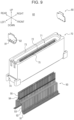
- FIG. 8 is a top perspective view of the connection object 60 to be connected to the connector 10 of FIG. 3 .
- FIG. 9 is an exploded top perspective view of the connection object 60 of FIG. 8 .
- connection object 60 includes, as large components, the insulator 70, the fittings 80, and the contacts 90.
- the connection object 60 is assembled by press-fitting the fittings 80 from above into the insulator 70 and press-fitting the contacts 90 from below into the insulator 70.
- the insulator 70 is a rectangular prism-shaped member made of an insulating heat-resistant synthetic resin material formed by injection molding.
- the insulator 70 includes a mating depression 71 recessed from an upper surface of the insulator 70.
- the insulator 70 includes a mating protrusion 72 located in the mating depression 71.
- the insulator 70 includes a guide 73 extending across an upper edge of the mating depression 71 and surrounding the mating depression 71.
- the guide 73 is defined by a sloping face that slopes obliquely downward and inward from the upper edge of the mating depression 71.
- the second restricting portions 23b of the first insulator 20 restrict excessive movement of the second insulator 30 relative to the first insulator 20 in the front-rear direction.
- the second insulator 30 significantly moves to an extent that exceeds a design value in the front-rear direction in response to elastic deformation of the contacts 50, the second restricted portions 37b of the second insulator 30 contact the second restricting portions 23b.
- the second insulator 30 does not further move outward in the front-rear direction.
- the restricting portions 44 of the fittings 40 reduce upward removal of the second insulator 30 from the first insulator 20.
- the restricting portions 44 of the fittings 40 restrict excessive upward movement of the second insulator 30 relative to the first insulator 20.
- the second insulator 30 significantly moves upward to an extent that exceeds a design value in response to elastic deformation of the contacts 50, the retaining protrusions 36 of the second insulator 30 contact the restricting portions 44.
- the second insulator 30 does not further move upward.
- the connector 10 can restrict excessive upward movement of the second insulator 30 with high-strength members like the fittings 40.
- connection object 60 inverted in the up-down direction is positioned to face the connector 10 including the above-described floating structure in the up-down direction while the connection object 60 is being substantially aligned with the connector 10 in the front-rear and left-right directions. Then, the connection object 60 is moved downward. If the connector 10 and the connection object 60 are slightly misaligned with each other in, for example, the front-rear and/or left-right direction, the guide 34 of the connector 10 and the guide 73 of the connection object 60 will contact each other.
- each of the contacts 50 of the connector 10 contacts the respective one of the contacts 90 of the connection object 60 in the mated state in which the second insulator 30 of the connector 10 and the insulator 70 of the connection object 60 are mated with each other. More specifically, the contact part 59a of the contact 50 contacts the contact portion 95 of the contact 90. At this time, the elastic contact piece 59 of the contact 50 is slightly elastically deformed outward in the front-rear direction, and is elastically displaced outward in the front-rear direction in the contact attachment groove 35.
- the restricting portions 44 of the fittings 40 press-fitted in the first insulator 20, illustrated in FIG. 3 can reduce the removal of the second insulator 30.
- Each of the restricting portions 44 in the first insulator 20 is located directly above the respective one of the retaining protrusions 36 of the second insulator 30. Therefore, when the second insulator 30 begins to move upward, the retaining protrusions 36 protruding outward contact the restricting portions 44. Thus, the second insulator 30 does not further move upward.
- the second holding portion 58 of the contact 50 engaging the contact attachment groove 35 of the second insulator 30 is displaced rearward.
- the portion of the contact 50 extending upward from the curved portion 56 is significantly elastically displaced rearward about the center, serving as a fulcrum, of a curve defined by the curved portion 56.
- the positions of the components located on the rear side relative to the curved portion 56 in the contact 50 hardly change before and after the movement of the second insulator 30.
- the connector 10 can reduce a load that is applied to the mounting portion 52 of each contact 50 even when reduced in size.
- the contact 50 is elastically deformed, as illustrated as examples in FIGs. 11A and 11B , due to compatibility between the above-described two advantages, or the improved flexibility of the contact 50 and the ease of determining the fulcrum of elastic deformation.
- the portion of the contact 50 extending from the curved portion 56 toward the removal side significantly elastically deforms about the center, serving as the fulcrum, of the curve of the curved portion 56, whereas the portion of the contact 50 located outside relative to the curved portion 56 in the front-rear direction hardly elastically deforms.
- Such a portion of the contact 50 that is to significantly elastically deform and the fulcrum of elastic deformation are at a long distance from the mounting portion 52 in the contact 50. Therefore, even if the connector 10 is reduced in size and the contact 50 is accordingly reduced in size, the connector 10 can reduce a load that is applied to the mounting portion 52 as the contact 50 undergoes elastic deformation.
- the contact 50 further includes the coupling portion 55 coupling the first extending portion 54 and the curved portion 56, resulting in a longer distance from the mounting portion 52 to the portion that is to significantly elastically deform and the fulcrum of elastic deformation in the contact 50. Therefore, even if the connector 10 is reduced in size and the contact 50 is accordingly reduced in size, the connector 10 can further reduce a load that is applied to the mounting portion 52 as the contact 50 undergoes elastic deformation.
- the coupling portion 55 slopes linearly from the end part of the first extending portion 54 adjacent to the second insulator 30 toward the mating side, so that the first extending portion 54 and the curved portion 56 can be coupled by the shortest distance.
- the connector 10 can reduce an unnecessary increase in distance between the first extending portion 54 and the curved portion 56 in the contact 50, thus reducing loss in signal transmission. Therefore, the connector 10 can reduce, for example, a decrease in transmission characteristics for high-capacity and high-speed transmission.
- the coupling portion 55 has the same width as that of the first extending portion 54, the second extending portion 57 and the combination of the first extending portion 54 and the coupling portion 55 in front of and behind the curved portion 56 are wider than the curved portion 56.
- a narrow portion of the contact 50 is limited to the curved portion 56.
- the length of the narrow portion can be further reduced. Therefore, when the contact 50 elastically deforms in response to movement of the second insulator 30, the fulcrum of elastic deformation can be more easily determined at a specific position in the curved portion 56. For example, the center of the curve of the curved portion 56 can be more stably determined as the fulcrum. Therefore, the connector 10 can achieve more stable movement of the second insulator 30 with a more stable fulcrum of elastic deformation of the contact 50.
- Each contact 50 is made of a metal material having a low elastic modulus. This allows the connector 10 to ensure a necessary movable distance for the second insulator 30 even when a small force is applied to the second insulator 30.
- the second insulator 30 can move smoothly relative to the first insulator 20. This allows the connector 10 to readily absorb misalignment when mated with the connection object 60.
- the fittings 40 are press-fitted in the first insulator 20, and the mounting portions 41 are soldered to the circuit board CB1.
- the fittings 40 enable the first insulator 20 to be stably fixed to the circuit board CB1.
- the fittings 40 increase the strength of mounting of the first insulator 20 on the circuit board CB1.
- the shape, size, location, and orientation of each component described above and the number of components are not limited to those illustrated in the above description and the figures. Any number of components having any shape, size, location, and orientation may be used as long as the function of the component can be achieved.
- connection object 60 The above-described assembly methods for the connector 10 and the connection object 60 are not limited to details in the above description. Each of the connector 10 and the connection object 60 may be assembled in any manner that allows the functions to be achieved.
- the curved portion 56 is shaped such that the entire curved portion 56 including the first end on the mating side has a smaller width than the first extending portion 54 and the second extending portion 57 in the left-right direction.
- the configuration is not limited to this example.
- the curved portion 56 may be shaped such that one part of the curved portion 56, for example, the first end, has a smaller width than the first extending portion 54 and the second extending portion 57 in the left-right direction.
- FIG. 12A is an enlarged side view of part of the contact 50 in FIG. 4 .
- FIG. 12B is an enlarged side view of a contact 50 in an alternative embodiment.
- An enlarged part of the contact 50 in each of FIGs. 12A and 12B corresponds to that of the contact 50 in the enlarged side view of FIG. 6 .
- the contact 50 further includes the coupling portion 55 coupling the first extending portion 54 and the curved portion 56.
- the first extending portion 54 includes a part horizontally extending from the end of the bend in the bent portion 53 toward the second insulator 30 and the end part located adjacent to the second insulator 30 and bent toward the mating side.
- the first extending portion 54 includes a portion extending from two vertical lines next to the bent portion 53 to a sloping broken line.
- the coupling portion 55 includes a portion extending linearly from the broken line to two oblique lines.
- the contact 50 may include no coupling portion 55.
- the first extending portion 54 and the curved portion 56 may be connected directly to each other in the contact 50.
- the first extending portion 54 includes the part horizontally extending from the end of the bend in the bent portion 53 toward the second insulator 30 and the end part located adjacent to the second insulator 30 and bent toward the mating side.
- the first extending portion 54 includes a part extending from two vertical lines next to the bent portion 53 to two oblique lines.
- the curved portion 56 is bent at an acute angle less than 90° from a lower end of the first extending portion 54 and includes an arc-shaped end part that is bent upward.
- the curved portion 56 is shaped like an arc of a sector having an obtuse central angle greater than 90°.
- the coupling portion 55 has the same width as that of the first extending portion 54.
- the configuration is not limited to this example.
- the coupling portion 55 may have any width larger than that of the curved portion 56.
- the coupling portion 55 may have a width larger than that of the curved portion 56 and smaller than that of the first extending portion 54.
- the coupling portion 55 may have a width larger than that of the first extending portion 54.
- the portion of the contact 50 extending from the curved portion 56 toward the removal side deforms elastically in response to movement of the second insulator 30.
- the configuration is not limited to this example.
- Another portion of the contact 50 may deform elastically in response to movement of the second insulator 30 as long as a load that is applied to the mounting portion 52 of the contact 50 can be reduced even when the connector 10 is reduced in size.
- the first distance L1 is equal to or less than half the second distance L2.
- the configuration is not limited to this example.
- the first distance L1 may be greater than half the second distance L2 as long as a decrease in the ease of forming the contact 50 and a decrease in transmission characteristics can be reduced.
- the width direction of each contact 50 is parallel to the array direction of the multiple contacts 50.
- the configuration is not limited to this example.
- the width direction of each contact 50 may be parallel to any direction orthogonal to the array direction of the multiple contacts 50 as long as the above-described function of the contact 50 can be achieved.
- FIG. 13 is a cross-sectional view, which is equivalent to FIG. 5 , illustrating a cross-section of a connector 10 according to an alternative embodiment.
- the connector 10 has a height, as illustrated in FIG. 5 , from the circuit board CB1, or the lower surfaces of the mounting portions 52 of the contacts 50, as a reference.
- the first insulator 20 has a height slightly larger than that of the mating protrusion 32 of the second insulator 30.
- the configuration is not limited to this example.
- the connector 10 may have a height, as illustrated in FIG. 13 , from the circuit board CB1, or the lower surfaces of the mounting portions 52 of the contacts 50, as a reference.
- the height of the connector 10 may be in the range of from 1.1 to 1.5 times the height of the connector 10 of FIG. 5 .
- the height of the connector 10 of FIG. 13 is approximately 1.4 times the height of the connector 10 of FIG. 5 .
- the height of the mating protrusion 32 of the second insulator 30 is the same as that of the mating protrusion 32 in FIG. 5 .
- the height of the first insulator 20 is approximately two times the height of the mating protrusion 32.
- each contact 50 that is to elastically deform in response to movement of the second insulator 30, or that extends from the curved portion 56 toward the removal side, is longer than that in the connector 10 of FIG. 5 . Therefore, the contact 50 exhibits improved flexibility. This further facilitates elastic deformation of the contact 50. This results in a further reduction in load that is applied to the mounting portion 52 of the contact 50.
- the first insulator 20 includes a thick wall with, for example, no cut on its outer surface.
- the configuration is not limited to this example.
- the outer surface of the first insulator 20 may include at least one cut.
- the first insulator 20 may include a cut extending in the up-down direction at a position between one contact 50 and another contact 50 adjacent to the one contact 50 in the left-right direction.
- Such a cut may extend from, for example, just above the contact attachment groove 25 to an upper surface of the outer peripheral wall 22.
- such a cut may be recessed from the outer surface of the first insulator 20 in the front-rear direction and be formed in at least one portion of the width of the outer peripheral wall 22 in the front-rear direction.
- the first extending portion 54 of each contact 50 horizontally extends from the end of the bent portion 53 adjacent to the second insulator 30 toward the second insulator 30.
- the configuration is not limited to this example.
- the first extending portion 54 may obliquely extend from the end of the bent portion 53 adjacent to the second insulator 30 toward the second insulator 30.
- the second extending portion 57 of each contact 50 has a linear shape and is parallel to the up-down direction.
- the configuration is not limited to this example.
- the second extending portion 57 may be non-parallel to the up-down direction or may have a non-linear shape.
- the first holding portion 51 of each contact 50 has a large width in the left-right direction so that the first holding portion 51 can engage the contact attachment groove 25 of the first insulator 20.
- the configuration is not limited to this example.
- the first holding portion 51 does not necessarily need to have a large width in the left-right direction for insert molding, rather than press-fitting.
- the contact 50 is made of a metal material having a low elastic modulus as described above, the configuration is not limited to this example.
- the contact 50 may be made of a metal material having any elastic modulus that allows the contact 50 to elastically deform by a necessary amount.
- connection object 60 has been described as a plug connector connected to the circuit board CB2.
- the connection object 60 is not limited to this example.
- the connection object 60 may be any object other than a connector.
- the connection object 60 may be an FPC, a flexible flat cable, a rigid board, or an edge connector of any circuit board.
- the above-described connector 10 is mounted on an electronic device.
- the electronic device include any on-vehicle equipment such as a camera, a radar, a dashboard camera, and an engine control unit.
- Examples of the electronic device include any on-vehicle equipment used in on-vehicle systems such as a car navigation system, an advanced driver assistance system, and a security system.
- Examples of the electronic device include any information equipment such as a personal computer, a smartphone, a copier, a printer, a facsimile, and a multifunctional machine.
- examples of the electronic device include any industrial equipment.
- the connector 10 with a floating structure can reduce a load that is applied to the mounting portions 52 of the contacts 50 even when reduced in size. This reduces breakage such as cracking of solder joints at the mounting portions 52 of the contacts 50. This reduces problems such as deformation and breakage of the contacts 50. This results in improved reliability of the electronic device, serving as a product, including the connector 10.
- the connector 10 absorbs misalignment between circuit boards with a good floating structure, thus improving the ease of assembly of the electronic device. This facilitates manufacture of the electronic device. Since the connector 10 reduces breakage of joints between the circuit board CB1 and the connector 10, the reliability of the electronic device as a product is further improved.
Landscapes
- Coupling Device And Connection With Printed Circuit (AREA)
Abstract
Description
- The present application claims priority to
Japanese Patent Application No. 2022-081182, filed on May 17, 2022 - The present disclosure relates to a connector and an electronic device.
- A connector with a floating structure has been known as a technology for improving the reliability of connection with a connection object. Such a connector absorbs misalignment between the connector and a connection object by using movement of a movable insulator as a component of the connector, for example, during and even after mating of the connector with the connection object. Patent Literature 1 discloses a connector that ensures smooth movement of such a movable insulator.
- Patent Literature 1:
Japanese Patent No. 5946804 - In an embodiment of the present disclosure, a connector includes a first insulator, a second insulator, and multiple contacts. The first insulator has a frame shape. The second insulator is disposed within the first insulator and is movable relative to the first insulator. The second insulator is to be mated with a connection object. The multiple contacts are attached to the first insulator and the second insulator. The multiple contacts each include a mounting portion, a holding portion, a bent portion, a first extending portion, a curved portion, and a second extending portion. The holding portion extends from the mounting portion along the first insulator and is attached to the first insulator. The bent portion is bent from the holding portion and extends toward the second insulator. The first extending portion extends from an end of a bend in the bent portion toward the second insulator. The curved portion is curved toward a removal side opposite to a mating side where the connection object is mated with the second insulator. The second extending portion extends from the curved portion toward the removal side. The curved portion includes a first end on the mating side and is bent and curved with the first end located on the mating side relative to the first extending portion. The first end has a smaller width than the first and second extending portions.
- In an embodiment of the present disclosure, an electronic device includes the above-described connector.
-
-
FIG. 1 is a top perspective view of a connector according to an embodiment connected to a connection object. -
FIG. 2 is a top perspective view of a connector according to an embodiment separated from a connection object. -
FIG. 3 is a top perspective view of the connector alone inFIG. 1 . -
FIG. 4 is an exploded top perspective view of the connector ofFIG. 3 . -
FIG. 5 is a cross-sectional view taken along arrow line V-V inFIG. 3 . -
FIG. 6 is an enlarged view of part VI surrounded by an alternate long and short dash line inFIG. 5 . -
FIG. 7 is an enlarged top perspective view of parts of contacts inFIG. 4 . -
FIG. 8 is a top perspective view of a connection object to be connected to the connector ofFIG. 3 . -
FIG. 9 is an exploded top perspective view of the connection object ofFIG. 8 . -
FIG. 10 is a cross-sectional view taken along arrow line X-X inFIG. 1 . -
FIG. 11A is a schematic diagram illustrating a first example of elastic deformation of a contact. -
FIG. 11B is a schematic diagram illustrating a second example of elastic deformation of the contact. -
FIG. 12A is an enlarged side view of part of the contact inFIG. 4 . -
FIG. 12B is an enlarged side view of part of a contact in an alternative embodiment. -
FIG. 13 is a cross-sectional view, which is equivalent toFIG. 5 , illustrating a cross-section of a connector according to an alternative embodiment. - In a connector with a floating structure, as a movable insulator moves, contacts attached to the movable insulator deform elastically. The elastic deformation of the contacts causes a restoring force, which in turn applies stress to mounting portions of the contacts on a circuit board. Under large stress loads on the mounting portions, the mounting portions are likely to break. For example, solder joints between the mounting portions and the circuit board may crack.
- Such a problem related to loads on the mounting portions becomes more pronounced as the connector is reduced in size. As various electronic devices have recently been miniaturized, connectors to be connected to connection objects are also required to achieve area savings and have a lower profile. Achieving area savings in a connector involves a reduction in distance between elastically deformable portions of contacts and mounting portions thereof. Thus, the mounting portions are more likely to experience a larger load.
- In an embodiment of the present disclosure, a connector and an electronic device can reduce a load that is applied to mounting portions of contacts even when reduced in size.
- An embodiment of the present disclosure will be described in detail below with reference to the accompanying drawings. In the following description, front-rear, left-right, and up-down directions are based on directions of arrows in the figures. The directions of the arrows in different figures,
FIGs. 1 to 7 andFIGs. 10 to 13 , are consistent with each other. The directions of the arrows inFIGs. 8 and9 are consistent with each other. For simplification of illustration, circuit boards CB1 and CB2, which will be described later, are not illustrated in some of the figures. -
FIG. 1 is a top perspective view of aconnector 10 according to an embodiment connected to aconnection object 60.FIG. 2 is a top perspective view of theconnector 10 according to an embodiment separated from theconnection object 60. As illustrated inFIG. 2 , for example, theconnector 10 includes afirst insulator 20 as a fixed insulator, asecond insulator 30 as a movable insulator,fittings 40, andcontacts 50. Theconnection object 60 includes aninsulator 70,fittings 80, andcontacts 90. - In an embodiment, for example, the
connector 10 will be hereinafter described as a receptacle connector, and theconnection object 60 will be hereinafter described as a plug connector. In theconnector 10 described as a receptacle connector, a portion of each of thecontacts 50 that is in contact with a respective one of thecontacts 90 is elastically deformed in a mated state in which thesecond insulator 30 of theconnector 10 and theconnection object 60 are mated with each other. On the other hand, in theconnection object 60 described as a plug connector, a portion of each of thecontacts 90 that is in contact with a respective one of thecontacts 50 is not elastically deformed in the mated state. The types of theconnector 10 and theconnection object 60 are not limited to those in this example. For example, theconnector 10 may serve as a plug connector, and theconnection object 60 may serve as a receptacle connector. - In the following description, the
connector 10 is mounted on the circuit board CB1, and theconnection object 60 is mounted on the circuit board CB2. Theconnector 10 electrically connects the circuit board CB1 to the circuit board CB2, on which theconnection object 60 is mounted, via theconnection object 60 mated with thesecond insulator 30 of theconnector 10. Each of the circuit boards CB1 and CB2 may be a rigid board or may be any other circuit board. For example, at least one of the circuit board CB1 or the circuit board CB2 may be an FPC (flexible printed circuit board). - In the following description, the
connector 10 and theconnection object 60 are connected to each other in a direction perpendicular to the circuit boards CB1 and CB2. For example, theconnector 10 and theconnection object 60 are connected to each other in the up-down direction. A mating direction in which thesecond insulator 30 and theconnection object 60 are mated with each other is orthogonal to the circuit board CB1. - The manner of connection is not limited to this example. The
connector 10 and theconnection object 60 may be connected to each other in a direction parallel to the circuit boards CB1 and CB2. Theconnector 10 and theconnection object 60 may be connected to each other such that one of theconnector 10 and theconnection object 60 is perpendicular to the circuit board on which the one of them is mounted and such that the other one of theconnector 10 and theconnection object 60 is parallel to the circuit board on which the other one of them is mounted. - As used herein, the "mating direction" refers to, for example, the up-down direction. A "lateral direction of the
connector 10" refers to, for example, the front-rear direction. A "longitudinal direction of theconnector 10" refers to, for example, the left-right direction. An "array direction of themultiple contacts 50" refers to, for example, the left-right direction. A "mating side" refers to, for example, a lower side. A "removal side" refers to, for example, an upper side. - The "mated state" refers to a state in which the
second insulator 30 of theconnector 10 and theconnection object 60 are mated with each other and in which eachcontact 50 is elastically deformed in contact with thecorresponding contact 90. An "unmated state" refers to a state in which thesecond insulator 30 of theconnector 10 and theconnection object 60 are not mated with each other and in which eachcontact 50 is not elastically deformed by an external force. - In an embodiment, the
connector 10 includes a floating structure. Theconnector 10 allows theconnection object 60 connected to theconnector 10 to move relative to the circuit board CB1 in six directions, or upward, downward, frontward, rearward, leftward, and rightward directions. Even while being connected to theconnector 10, theconnection object 60 is movable relative to the circuit board CB1 in the six directions, or the upward, downward, frontward, rearward, leftward, and rightward directions, within a predetermined range. In addition to the six directions, or the upward, downward, frontward, rearward, leftward, and rightward directions, theconnection object 60 is movable in, for example, oblique directions between the respective directions within the predetermined range. -
FIG. 3 is a top perspective view of theconnector 10 alone inFIG. 1 .FIG. 4 is an exploded top perspective view of theconnector 10 ofFIG. 3 .FIG. 5 is a cross-sectional view taken along arrow line V-V inFIG. 3 .FIG. 6 is an enlarged view of part VI surrounded by an alternate long and short dash line inFIG. 5 .FIG. 7 is an enlarged top perspective view of parts of thecontacts 50 inFIG. 4 . - As illustrated in
FIG. 4 , theconnector 10 is assembled in the following manner, for example. Thefittings 40 are press-fitted from below into thefirst insulator 20. Thesecond insulator 30 is disposed from below into thefirst insulator 20 with thefittings 40. Thecontacts 50 are press-fitted from below into thefirst insulator 20 and thesecond insulator 30, which is disposed within thefirst insulator 20. - The configurations of components of the
connector 10 in the unmated state will be primarily described below. First, the configuration of thefirst insulator 20 will be primarily described with reference primarily toFIG. 4 . - As illustrated in
FIG. 4 , thefirst insulator 20 is a member made of an insulating heat-resistant synthetic resin material formed by injection molding, and extends in the left-right direction. Thefirst insulator 20 is frame-shaped. Thefirst insulator 20 is hollow and includes anopening 21a at an upper surface of thefirst insulator 20 and anopening 21b at a lower surface thereof. Thefirst insulator 20 includes an outerperipheral wall 22 including four sides and surrounding an internal space of thefirst insulator 20. More specifically, the outerperipheral wall 22 includes a pair oflateral walls 22a disposed one each at opposite sides in the left-right direction and a pair oflongitudinal walls 22b disposed one each at opposite sides in the front-rear direction. The pair oflateral walls 22a and the pair oflongitudinal walls 22b are orthogonal to each other, thus forming the outerperipheral wall 22. - The
first insulator 20 includes first restrictingportions 23a extending in the up-down direction on inner surfaces of thelateral walls 22a. Each of the first restrictingportions 23a is located at the middle of an upper end portion of the inner surface of thelateral wall 22a in the front-rear direction and has a predetermined width in the front-rear direction. The first restrictingportion 23a protrudes inward from the inner surface of thelateral wall 22a in the left-right direction and is formed as a stepped portion on the inner surface. Thefirst insulator 20 includes second restrictingportions 23b extending in the up-down direction on inner surfaces of thelongitudinal walls 22b. The second restrictingportions 23b are located one each at opposite ends of an upper end portion of the inner surface of each of thelongitudinal walls 22b in the left-right direction. Each of the second restrictingportions 23b has a predetermined width in the left-right direction. The second restrictingportion 23b protrudes inward from the inner surface of thelongitudinal wall 22b in the front-rear direction and is formed as a stepped portion on the inner surface. - The
first insulator 20 includes afitting attachment groove 24 located in a lower portion of each of thelateral walls 22a and recessed in thefirst insulator 20. The fitting 40 is attached to thefitting attachment groove 24. - The
first insulator 20 includes multiplecontact attachment grooves 25 located in a lower end portion of the inner surface of each of thelongitudinal walls 22b and extending in the up-down direction. Each of themultiple contacts 50 is attached to a respective one of the multiplecontact attachment grooves 25. The multiplecontact attachment grooves 25 are spaced apart from each other at predetermined intervals in the left-right direction and are recessed. - The configuration of the
second insulator 30 will be described with reference primarily toFIG. 4 . Thesecond insulator 30 is disposed into the internal space surrounded by the outerperipheral wall 22 of thefirst insulator 20 through theopening 21b, and is movable relative to thefirst insulator 20. Thesecond insulator 30 is to be mated with theconnection object 60. - The
second insulator 30 is a member made of an insulating heat-resistant synthetic resin material formed by injection molding, and extends in the left-right direction. Thesecond insulator 30 is inverted T-shaped as viewed from the front. Thesecond insulator 30 includes abase 31, serving as a lower portion of thesecond insulator 30, extending in the left-right direction. Thesecond insulator 30 includes awall portion 31a located in thebase 31 and having a small width in the front-rear direction. Thewall portion 31a extends across the base 31 in the up-down direction. Thewall portion 31a extends substantially across the base 31 in the left-right direction, except for opposite ends of the base 31 in the left-right direction. As illustrated inFIG. 5 , a lower end part of thewall portion 31a tapers toward the mating side in the up-down direction. - As illustrated in
FIG. 4 , thesecond insulator 30 includes amating protrusion 32 protruding upward from thebase 31 and being to be mated with theconnection object 60. Themating protrusion 32 is slightly larger than the base 31 in the left-right direction, and protrudes from opposite sides of the base 31 in the left-right direction. - The
second insulator 30 includes amating depression 33 recessed from an upper surface of themating protrusion 32. Thesecond insulator 30 includes aguide 34 extending across an upper edge of themating protrusion 32 and surrounding themating depression 33. Theguide 34 is defined by a sloping face that slopes obliquely downward and outward from the upper edge of themating protrusion 32. - The
second insulator 30 includes multiplecontact attachment grooves 35 located in themating protrusion 32 and extending substantially across themating protrusion 32 in the up-down direction. Each of themultiple contacts 50 is attached to the respective one of the multiplecontact attachment grooves 35. Thecontact attachment grooves 35 are spaced apart from each other at predetermined intervals in the left-right direction and are recessed. - As illustrated in
FIG. 5 , thecontact attachment grooves 35 extend from the bottom of themating protrusion 32 to the top thereof, or through themating protrusion 32. A lower end of each of thecontact attachment grooves 35 is exposed on the bottom of themating protrusion 32 and is continuous with thewall portion 31a. Portions of thecontact attachment grooves 35 that extend upward from the lower ends of thecontact attachment grooves 35 are formed and recessed from both inner surfaces of themating depression 33 in the front-rear direction. - As illustrated in
FIG. 4 , thesecond insulator 30 includes retainingprotrusions 36 located one each on opposite ends of a lower end of the base 31 in the left-right direction and protruding outward in the left-right direction. Thesecond insulator 30 includes first restrictedportions 37a defined by outer surfaces of thesecond insulator 30 in the left-right direction. The firstrestricted portions 37a include outer surfaces of the base 31 in the left-right direction and outer surfaces of an inward-stepped lower end of themating protrusion 32 in the left-right direction. The inward-stepped lower end is reduced in dimension in the front-rear and left-right directions. Thesecond insulator 30 includes second restrictedportions 37b defined by outer surfaces of thesecond insulator 30 in the front-rear direction. The secondrestricted portions 37b include outer surfaces of outward-stepped portions of the base 31 located at opposite ends of an upper end portion of the base 31 in the left-right direction and protruding outward in the front-rear direction, and further include outer surfaces of the inward-stepped lower end, which is reduced in dimension in the front-rear and left right directions, of themating protrusion 32 in the front-rear direction. - The configuration of each fitting 40 will be described with reference primarily to
FIG. 4 . - The fitting 40 is formed by shaping a sheet of any metal material into a form illustrated in
FIG. 4 with a progressive die (stamping). The method of forming the fitting 40 includes, after stamping, bending a workpiece in a thickness direction of the workpiece. The fitting 40 is substantially inverted U-shaped as viewed in the left-right direction. - The fitting 40 includes mounting
portions 41 located at lower ends of the fitting 40 at opposite sides thereof in the front-rear direction and extending outward to define an L-shape. The fitting 40 includes engagingportions 42 each extending upward from an upper end of a respective one of the mountingportions 41. The fitting 40 includes a base 43 extending in the front-rear direction to couple the engagingportions 42 at the opposite sides of the fitting 40 in the front-rear direction. The fitting 40 includes a restrictingportion 44 located at the middle of the base 43 in the front-rear direction, protruding outward in the left-right direction, and having a relatively large width in the left-right direction. - The configuration of each
contact 50 will be described with reference primarily toFIGs. 4 to 7 . - The
contact 50 is formed by shaping a sheet of, for example, a copper alloy containing, for example, phosphor bronze, beryllium copper, or titanium copper, and having spring elasticity or a Corson alloy into a form illustrated inFIGs. 4 to 7 with a progressive die (stamping). Thecontact 50 is formed by stamping the sheet into a workpiece and then bending the workpiece in a thickness direction of the workpiece. The method of forming thecontact 50 is not limited to this example. The method may include only stamping. Thecontact 50 is made of, for example, a metal material having a low elastic modulus, to produce a significant change in shape associated with elastic deformation. Thecontact 50 is plated with nickel, serving as an undercoat layer, and is then plated with, for example, gold or tin. - As illustrated in
FIG. 4 , themultiple contacts 50 are arrayed in the longitudinal direction of theconnector 10. As illustrated inFIG. 5 , thecontacts 50 are attached to thefirst insulator 20 and thesecond insulator 30. A pair ofcontacts 50 arrayed at the same position in the left-right direction are symmetrically shaped and arranged in the front-rear direction. The pair ofcontacts 50 are shaped and arranged symmetrically with respect to a centerline or axis extending therebetween in the up-down direction. - Each of the
contacts 50 includes a first holdingportion 51 extending in the up-down direction and supported by thefirst insulator 20. Thecontact 50 includes a mountingportion 52 extending outward from a lower end of the first holdingportion 51 to define an L-shape. Thefirst holding portion 51 extends from the mountingportion 52 along thefirst insulator 20 and is disposed along thefirst insulator 20. Thecontact 50 includes abent portion 53 bent from an upper end of the first holdingportion 51 and extending toward thesecond insulator 30. - The
contact 50 includes a first extendingportion 54 extending from an end of a bend in thebent portion 53 toward thesecond insulator 30. The first extendingportion 54 extends horizontally from an end of thebent portion 53 adjacent to thesecond insulator 30 toward thesecond insulator 30. An end part of the first extendingportion 54 adjacent to thesecond insulator 30 is bent toward the mating side where theconnection object 60 is mated with thesecond insulator 30. - The
contact 50 includes acoupling portion 55 sloping linearly from the end part of the first extendingportion 54 adjacent to thesecond insulator 30 toward the mating side. Thecontact 50 includes acurved portion 56 curved from a lower end of thecoupling portion 55 toward the removal side opposite to the mating side. Thecurved portion 56 is coupled to the first extendingportion 54 by thecoupling portion 55. - The
contact 50 includes a second extendingportion 57 extending from thecurved portion 56 toward the removal side. The second extendingportion 57 has a linear shape and is parallel to the up-down direction. Thecontact 50 includes asecond holding portion 58 bent inward in the front-rear direction from an upper end of the second extendingportion 57 and extending linearly upward. Thesecond holding portion 58 includes abent part 58a smoothly bent in a crank-shape from the upper end of the second extendingportion 57. Thesecond holding portion 58 includes a wide part located directly on thebent part 58a and having a large width in the left-right direction. Thesecond holding portion 58 is supported by thesecond insulator 30. - The
contact 50 includes anelastic contact piece 59 extending upward from an upper end of the second holdingportion 58 and slightly inclined inward in the front-rear direction. Theelastic contact piece 59 includes an upper end portion and an innermost portion. The upper end portion is bent obliquely downward and inward in the front-rear direction. The innermost portion is located at an innermost position in the front-rear direction and is bent obliquely downward and outward in the front-rear direction. Theelastic contact piece 59 includes acontact part 59a located at the innermost position in the front-rear direction. - As illustrated in
FIG. 6 , the first holdingportion 51 of thecontact 50 engages thecontact attachment groove 25 located in thelongitudinal wall 22b of thefirst insulator 20. Thefirst holding portion 51 is attached to thefirst insulator 20. As illustrated inFIG. 5 , the second holdingportion 58 of thecontact 50 engages thecontact attachment groove 35 located in themating protrusion 32 of thesecond insulator 30. - Once the
multiple contacts 50 are attached to thefirst insulator 20 and thesecond insulator 30, thecontact part 59a of each of thecontacts 50 is located in themating depression 33 of thesecond insulator 30. Theelastic contact piece 59 of eachcontact 50 is disposed in thecontact attachment groove 35 of thesecond insulator 30 and is elastically deformable in the front-rear direction. Eachcontact 50 supports thesecond insulator 30 such that thesecond insulator 30 is floating apart from thefirst insulator 20 in the internal space surrounded by the outerperipheral wall 22 of thefirst insulator 20. - Once the
second insulator 30 is held relative to thefirst insulator 20 by thecontacts 50, thesecond insulator 30 is located apart from thefirst insulator 20 in the internal space surrounded by the outerperipheral wall 22 of thefirst insulator 20. More specifically, thebase 31 of thesecond insulator 30 is located in the internal space, surrounded by the pair oflongitudinal walls 22b and the pair oflateral walls 22a, of thefirst insulator 20. Thebase 31 of thesecond insulator 30 is surrounded by the outerperipheral wall 22 of thefirst insulator 20. - The
mating protrusion 32 of thesecond insulator 30 protrudes upward through theopening 21a of thefirst insulator 20 and is located outside the internal space of thefirst insulator 20. Themating protrusion 32 of thesecond insulator 30 is located above the outerperipheral wall 22 of thefirst insulator 20 such that themating protrusion 32 can be mated with theconnection object 60. - At this time, the second
restricted portions 37b of thesecond insulator 30 face, from inside, the second restrictingportions 23b located on thelongitudinal walls 22b of thefirst insulator 20 in the front-rear direction. As illustrated inFIG. 3 , the firstrestricted portions 37a of thesecond insulator 30 face, from inside, the first restrictingportions 23a located on thelateral walls 22a of thefirst insulator 20 in the left-right direction. The retainingprotrusions 36 of thesecond insulator 30 face, from below, the restrictingportions 44 of thefittings 40. - The engaging
portions 42 of each of thefittings 40 engage thefitting attachment groove 24 of thefirst insulator 20. Thefittings 40 are press-fitted in thefitting attachment grooves 24 of thefirst insulator 20 and are located one each at the opposite ends of thefirst insulator 20 in the left-right direction. - The
bases 43 of thefittings 40 attached to thefirst insulator 20 are located at opposite ends of the internal space of thefirst insulator 20 in the left-right direction. Once thesecond insulator 30 is held relative to thefirst insulator 20 by thecontacts 50, a lower surface of the restrictingportion 44 of each of thebases 43 faces an upper surface of the respective one of the retainingprotrusions 36 of thesecond insulator 30 in the up-down direction. - As illustrated in
FIG. 6 , thebent portion 53 is bent at an angle of 90° from the upper end of the first holdingportion 51. Thebent portion 53 is shaped like an arc of a sector having a central angle of 90°. The end part of the first extendingportion 54 adjacent to thesecond insulator 30 is bent at an obtuse angle greater than 90°. This end part has a shape like an arc of a sector having an acute central angle less than 90°. Thecurved portion 56 is bent at an acute angle less than 90° from the lower end of thecoupling portion 55 sloping linearly, and includes an arc-shaped end part bent upward. Thecurved portion 56 is shaped like an arc of a sector having an obtuse central angle greater than 90°. - In each of the
contacts 50, the mountingportion 52, the first holdingportion 51, thebent portion 53, and part of the first extendingportion 54 are arranged along thefirst insulator 20. Thefirst insulator 20 is located between these elements of onecontact 50 and these elements of anothercontact 50 adjacent to the onecontact 50 in the left-right direction. - In the
contact 50, the end part of the first extendingportion 54 adjacent to thesecond insulator 30, thecoupling portion 55, thecurved portion 56, and the second extendingportion 57 are located between thefirst insulator 20 and thesecond insulator 30. Thefirst insulator 20 is not located between these elements of onecontact 50 and these elements of anothercontact 50 adjacent to the onecontact 50 in the left-right direction. - The
curved portion 56 includes a first end on the mating side and is bent and curved with the first end located on the mating side relative to the first extendingportion 54. The first extendingportion 54 includes a second end on the removal side. A first distance L1 in the mating direction from the second end to the first end of thecurved portion 56 on the mating side is equal to or less than half a second distance L2 in the mating direction from the circuit board CB1, or a lower surface of the mountingportion 52, to the second end. For example, the first distance L1 may be approximately 0.35 times the second distance L2. - As illustrated in
FIG. 7 , a width direction of eachcontact 50 is parallel to the array direction of themultiple contacts 50. A thickness direction of thecontact 50 is any direction orthogonal to the left-right direction and is included in planes in the up-down and front-rear directions. The thickness of thecontact 50 is substantially uniform at any point in thecontact 50. On the other hand, the width of thecontact 50 in the left-right direction varies at different points in thecontact 50. - The
first holding portion 51 of thecontact 50 has a large width in the left-right direction so that the first holdingportion 51 can engage thecontact attachment groove 25 of thefirst insulator 20. Thebent portion 53 has a smaller width than the first holdingportion 51 in the left-right direction. The first extendingportion 54 has a larger width than thebent portion 53 in the left-right direction. Thecoupling portion 55 has the same width as that of the first extendingportion 54 and is continuous with the first extendingportion 54, and has a larger width than thebent portion 53 in the left-right direction. - The
curved portion 56 has a smaller width than the first extendingportion 54 and thecoupling portion 55 in the left-right direction. The second extendingportion 57 has a larger width than thecurved portion 56 in the left-right direction and extends upward continuously from thecurved portion 56. For example, the second extendingportion 57 has substantially the same width as those of the first extendingportion 54 and thecoupling portion 55. Thecurved portion 56 is narrower in the left-right direction than the second extendingportion 57 in addition to the first extendingportion 54 and thecoupling portion 55. - Of the elements of the
contact 50 located between thefirst insulator 20 and thesecond insulator 30, thecurved portion 56 has the smallest width in the left-right direction. In a portion of thecontact 50 that is located between thefirst insulator 20 and thesecond insulator 30, only a bend corresponding to thecurved portion 56, which couples the second extendingportion 57 to the first extendingportion 54 and thecoupling portion 55, has a small width in the left-right direction. The first extendingportion 54 and thecoupling portion 55, which is next to the bend, and the second extendingportion 57, which is next to the bend, have a larger width than thecurved portion 56 in the left-right direction. - In the
contact 50, thebent portion 53 is narrow. The first extendingportion 54, which is next to thebent portion 53, and thecoupling portion 55 are wide. Thecurved portion 56, which is next to thecoupling portion 55 and the first extendingportion 54, is narrow. In addition, as illustrated inFIG. 4 , thecurved portion 56 is narrow, the second extendingportion 57 next to thecurved portion 56 is wide, and thebent part 58a of the second holdingportion 58 next to the second extendingportion 57 is narrow. As described above, thecontact 50 includes two portions in each of which a narrow part, a wide part, and a narrow part are arranged in that order, and the two portions are continuously formed. - The
connector 10 with the above-described structure is mounted on, for example, a circuit formation surface formed on a mounting surface of the circuit board CB1. More specifically, the mountingportions 41 of thefittings 40 are placed on a solder paste applied to a pattern on the circuit board CB1. The mountingportions 52 of thecontacts 50 are placed on the solder paste applied to the pattern on the circuit board CB1. The mountingportions 41 and the mountingportions 52 are soldered to the pattern by heating and melting the solder paste in, for example, a reflow furnace. Thus, the mounting of theconnector 10 on the circuit board CB1 is completed. For example, electronic components different from theconnector 10 and including a CPU (central processing unit), a controller, and a memory are mounted on the circuit formation surface of the circuit board CB1. - The structure of the
connection object 60 will be described with reference primarily toFIGs. 8 and9 . -
FIG. 8 is a top perspective view of theconnection object 60 to be connected to theconnector 10 ofFIG. 3 .FIG. 9 is an exploded top perspective view of theconnection object 60 ofFIG. 8 . - As illustrated in
FIG. 9 , theconnection object 60 includes, as large components, theinsulator 70, thefittings 80, and thecontacts 90. Theconnection object 60 is assembled by press-fitting thefittings 80 from above into theinsulator 70 and press-fitting thecontacts 90 from below into theinsulator 70. - The
insulator 70 is a rectangular prism-shaped member made of an insulating heat-resistant synthetic resin material formed by injection molding. Theinsulator 70 includes amating depression 71 recessed from an upper surface of theinsulator 70. Theinsulator 70 includes amating protrusion 72 located in themating depression 71. Theinsulator 70 includes aguide 73 extending across an upper edge of themating depression 71 and surrounding themating depression 71. Theguide 73 is defined by a sloping face that slopes obliquely downward and inward from the upper edge of themating depression 71. - The
insulator 70 includesfitting attachment grooves 74 located at opposite ends of a lower portion of theinsulator 70 in the left-right direction and recessed in the up-down direction. Each of thefittings 80 is attached to a respective one of thefitting attachment grooves 74. Theinsulator 70 includes multiplecontact attachment grooves 75 located on front and rear inner surfaces of the lower portion and front and rear surfaces of themating protrusion 72. Each of themultiple contacts 90 is attached to a respective one of the multiplecontact attachment grooves 75. The multiplecontact attachment grooves 75 are spaced apart from each other at predetermined intervals in the left-right direction. - Each of the
fittings 80 is formed by shaping a sheet of any metal material into a form illustrated inFIG. 9 with a progressive die (stamping). The fitting 80 is disposed on each of the opposite ends of theinsulator 70 in the left-right direction. The fitting 80 includes a mountingportion 81 located at a lower end of the fitting 80 and extending outward in the left-right direction to define an L-shape. The fitting 80 includes an engagingportion 82 extending upward continuously from the mountingportion 81 and being to engage theinsulator 70. - Each of the
contacts 90 is formed by shaping a sheet of, for example, a copper alloy containing, for example, phosphor bronze, beryllium copper, or titanium copper, and having spring elasticity or a Corson alloy into a form illustrated inFIG. 9 with a progressive die (stamping). Thecontact 90 is formed by stamping the sheet into a workpiece and then bending the workpiece in a thickness direction of the workpiece. The method of forming thecontact 90 is not limited to this example. The method may include only stamping. Thecontact 90 is plated with nickel, serving as an undercoat layer, and is then plated with, for example, gold or tin. - The
multiple contacts 90 are arrayed in the left-right direction. Each of thecontacts 90 includes an L-shaped mountingportion 91 extending outward in the front-rear direction. Thecontact 90 includes a first engagingportion 92 formed continuously with the mountingportion 91. Thecontact 90 includes acoupling portion 93 extending upward in a crank-shape from the first engagingportion 92. Thecontact 90 includes a second engagingportion 94 linearly extending upward from an upper end of thecoupling portion 93. Thecontact 90 includes acontact portion 95 linearly extending upward from an upper end of the second engagingportion 94. - As illustrated in
FIG. 8 , thefittings 80 are attached to thefitting attachment grooves 74 of theinsulator 70. For example, the engagingportions 82 of thefittings 80 engage thefitting attachment grooves 74 of theinsulator 70. Thefittings 80 are disposed one each on the opposite ends of theinsulator 70 in the left-right direction. - Each of the
multiple contacts 90 is attached to the respective one of the multiplecontact attachment grooves 75 of theinsulator 70. For example, the first engagingportion 92 and the second engagingportion 94 of thecontact 90 engage thecontact attachment groove 75 of theinsulator 70. At this time, thecontact portion 95 of thecontact 90 is located on themating protrusion 72 of theinsulator 70. Thecontact portion 95 of thecontact 90 faces outward in the front-rear direction within themating depression 71. - The
connection object 60 with the above-described structure is mounted on, for example, a circuit formation surface formed on a mounting surface of the circuit board CB2. More specifically, the mountingportions 81 of thefittings 80 are placed on a solder paste applied to a pattern on the circuit board CB2. The mountingportions 91 of thecontacts 90 are placed on the solder paste applied to the pattern on the circuit board CB2. The mountingportions 81 and the mountingportions 91 are soldered to the pattern by heating and melting the solder paste in, for example, a reflow furnace. Thus, the mounting of theconnection object 60 on the circuit board CB2 is completed. For example, electronic components different from theconnection object 60 and including a camera module and a sensor are mounted on the circuit formation surface of the circuit board CB2. -
FIG. 10 is a cross-sectional view taken along arrow line X-X inFIG. 1 . Operation of theconnector 10 with the floating structure will be primarily described with reference primarily toFIG. 10 . - Soldering the mounting
portions 52 of thecontacts 50 to the circuit board CB1 fixes thefirst insulator 20 to the circuit board CB1. Elastic deformation of thecontacts 50 enables thesecond insulator 30 to be movable relative to thefirst insulator 20 fixed to the circuit board CB 1. - As illustrated in
FIG. 3 , the second restrictingportions 23b of thefirst insulator 20 restrict excessive movement of thesecond insulator 30 relative to thefirst insulator 20 in the front-rear direction. For example, when thesecond insulator 30 significantly moves to an extent that exceeds a design value in the front-rear direction in response to elastic deformation of thecontacts 50, the secondrestricted portions 37b of thesecond insulator 30 contact the second restrictingportions 23b. Thus, thesecond insulator 30 does not further move outward in the front-rear direction. - The first restricting
portions 23a of thefirst insulator 20 restrict excessive movement of thesecond insulator 30 relative to thefirst insulator 20 in the left-right direction. For example, when thesecond insulator 30 significantly moves to an extent that exceeds a design value in the left-right direction in response to elastic deformation of thecontacts 50, the firstrestricted portions 37a of thesecond insulator 30 contact the first restrictingportions 23a. Thus, thesecond insulator 30 does not further move outward in the left-right direction. - The restricting
portions 44 of thefittings 40 reduce upward removal of thesecond insulator 30 from thefirst insulator 20. The restrictingportions 44 of thefittings 40 restrict excessive upward movement of thesecond insulator 30 relative to thefirst insulator 20. For example, when thesecond insulator 30 significantly moves upward to an extent that exceeds a design value in response to elastic deformation of thecontacts 50, the retainingprotrusions 36 of thesecond insulator 30 contact the restrictingportions 44. Thus, thesecond insulator 30 does not further move upward. Theconnector 10 can restrict excessive upward movement of thesecond insulator 30 with high-strength members like thefittings 40. - The
connection object 60 inverted in the up-down direction is positioned to face theconnector 10 including the above-described floating structure in the up-down direction while theconnection object 60 is being substantially aligned with theconnector 10 in the front-rear and left-right directions. Then, theconnection object 60 is moved downward. If theconnector 10 and theconnection object 60 are slightly misaligned with each other in, for example, the front-rear and/or left-right direction, theguide 34 of theconnector 10 and theguide 73 of theconnection object 60 will contact each other. - Thus, the floating structure of the
connector 10 allows thesecond insulator 30 to move relative to thefirst insulator 20. More specifically, themating protrusion 32 of thesecond insulator 30 is guided into themating depression 71 of theinsulator 70. As theconnection object 60 is further moved downward, themating protrusion 32 of thesecond insulator 30 and themating depression 71 of theinsulator 70 are mated with each other. At this time, themating depression 33 of thesecond insulator 30 and themating protrusion 72 of theinsulator 70 are mated with each other. - As illustrated in
FIG. 10 , each of thecontacts 50 of theconnector 10 contacts the respective one of thecontacts 90 of theconnection object 60 in the mated state in which thesecond insulator 30 of theconnector 10 and theinsulator 70 of theconnection object 60 are mated with each other. More specifically, thecontact part 59a of thecontact 50 contacts thecontact portion 95 of thecontact 90. At this time, theelastic contact piece 59 of thecontact 50 is slightly elastically deformed outward in the front-rear direction, and is elastically displaced outward in the front-rear direction in thecontact attachment groove 35. - The
connector 10 and theconnection object 60 are completely connected in the above-described manner. At this time, the circuit board CB1 and the circuit board CB2 are electrically connected by thecontacts 50 and thecontacts 90. - In such a state, one pair of
elastic contact pieces 59 of thecontacts 50 pinch one pair ofcontacts 90 of theconnection object 60 on the opposite sides in the front-rear direction with elastic forces acting inward in the front-rear direction. Thus, reaction of pressing forces applied to thecontacts 90 causes thesecond insulator 30 to experience a force acting in a removal direction, or the upward direction, via thecontacts 50 when theconnection object 60 is removed from theconnector 10. - Thus, if the
second insulator 30 moves upward, the restrictingportions 44 of thefittings 40 press-fitted in thefirst insulator 20, illustrated inFIG. 3 , can reduce the removal of thesecond insulator 30. Each of the restrictingportions 44 in thefirst insulator 20 is located directly above the respective one of the retainingprotrusions 36 of thesecond insulator 30. Therefore, when thesecond insulator 30 begins to move upward, the retainingprotrusions 36 protruding outward contact the restrictingportions 44. Thus, thesecond insulator 30 does not further move upward. -
FIG. 11A is a schematic diagram illustrating a first example of elastic deformation of thecontact 50.FIG. 11B is a schematic diagram illustrating a second example of elastic deformation of thecontact 50. AlthoughFIGs. 11A and11B each illustrate onecontact 50 located on the rear side inFIG. 5 , theother contact 50 at the same position in the front-rear direction elastically deforms in the same and/or similar manner. As forFIG. 11A , elastic deformation of therelevant contact 50 on the front side corresponds to a depiction ofFIG. 11B reversed in the front-rear direction. As forFIG. 11B , elastic deformation of therelevant contact 50 on the front side corresponds to a depiction ofFIG. 11A reversed in the front-rear direction. - Motions of the components of the
contact 50 during elastic deformation will be described in detail with reference toFIGs. 11A and11B . InFIGs. 11A and11B , a chain double-dashed line represents a state of thecontact 50 that is not elastically deformed. A portion of thecontact 50 that extends from thecurved portion 56 toward the removal side is elastically deformed as thesecond insulator 30 moves. - In
FIG. 11A , for example, it is assumed that thesecond insulator 30 is moved rearward by any external factor. - As the
second insulator 30 is moved rearward, the second holdingportion 58 of thecontact 50 engaging thecontact attachment groove 35 of thesecond insulator 30 is displaced rearward. At this time, the portion of thecontact 50 extending upward from thecurved portion 56 is significantly elastically displaced rearward about the center, serving as a fulcrum, of a curve defined by thecurved portion 56. On the other hand, the positions of the components located on the rear side relative to thecurved portion 56 in thecontact 50 hardly change before and after the movement of thesecond insulator 30. - In
FIG. 11B , for example, it is assumed that thesecond insulator 30 is moved frontward by any external factor. - As the
second insulator 30 is moved frontward, the second holdingportion 58 of thecontact 50 engaging thecontact attachment groove 35 of thesecond insulator 30 is displaced frontward. At this time, the portion of thecontact 50 extending upward from thecurved portion 56 is significantly elastically displaced frontward about the center, serving as the fulcrum, of the curve defined by thecurved portion 56. On the other hand, the positions of the components located on the rear side relative to thecurved portion 56 in thecontact 50 hardly change before and after the movement of thesecond insulator 30. - The following description will primarily focus on the
connector 10. Advantages of theconnector 10 will be described below. The same and/or similar description applies to an electronic device including theconnector 10. - In an embodiment, the
connector 10 can reduce a load that is applied to the mountingportion 52 of eachcontact 50 even when reduced in size. - The
connector 10 includes the first extendingportion 54 including the end part located adjacent to thesecond insulator 30 and bent toward the mating side and thecurved portion 56 curved toward the removal side opposite to the mating side. This increases the length of an elastically deformable portion, serving as a spring, of thecontact 50. This results in improved flexibility of thecontact 50 in theconnector 10. This facilitates elastic deformation of thecontact 50. This leads to a reduction in load that is applied to the mountingportion 52 of thecontact 50. - In the
connector 10, thecurved portion 56 is narrower than the first extendingportion 54 and the second extendingportion 57. Limiting a narrow portion of thecontact 50 to thecurved portion 56 can reduce the length of the narrow portion. Thus, when thecontact 50 elastically deforms in response to movement of thesecond insulator 30, the fulcrum of elastic deformation can be easily determined at a specific position in thecurved portion 56. For example, the center of the curve of thecurved portion 56 is easily and stably determined as the fulcrum. Therefore, theconnector 10 can achieve stable movement of thesecond insulator 30 with the stable fulcrum of elastic deformation of thecontact 50. - The
contact 50 is elastically deformed, as illustrated as examples inFIGs. 11A and11B , due to compatibility between the above-described two advantages, or the improved flexibility of thecontact 50 and the ease of determining the fulcrum of elastic deformation. As illustrated as examples inFIGs. 11A and11B , the portion of thecontact 50 extending from thecurved portion 56 toward the removal side significantly elastically deforms about the center, serving as the fulcrum, of the curve of thecurved portion 56, whereas the portion of thecontact 50 located outside relative to thecurved portion 56 in the front-rear direction hardly elastically deforms. Such a portion of thecontact 50 that is to significantly elastically deform and the fulcrum of elastic deformation are at a long distance from the mountingportion 52 in thecontact 50. Therefore, even if theconnector 10 is reduced in size and thecontact 50 is accordingly reduced in size, theconnector 10 can reduce a load that is applied to the mountingportion 52 as thecontact 50 undergoes elastic deformation. - The
contact 50 further includes thecoupling portion 55 coupling the first extendingportion 54 and thecurved portion 56, resulting in a longer distance from the mountingportion 52 to the portion that is to significantly elastically deform and the fulcrum of elastic deformation in thecontact 50. Therefore, even if theconnector 10 is reduced in size and thecontact 50 is accordingly reduced in size, theconnector 10 can further reduce a load that is applied to the mountingportion 52 as thecontact 50 undergoes elastic deformation. - The
coupling portion 55 slopes linearly from the end part of the first extendingportion 54 adjacent to thesecond insulator 30 toward the mating side, so that the first extendingportion 54 and thecurved portion 56 can be coupled by the shortest distance. Thus, theconnector 10 can reduce an unnecessary increase in distance between the first extendingportion 54 and thecurved portion 56 in thecontact 50, thus reducing loss in signal transmission. Therefore, theconnector 10 can reduce, for example, a decrease in transmission characteristics for high-capacity and high-speed transmission. - Since the
coupling portion 55 has the same width as that of the first extendingportion 54, the second extendingportion 57 and the combination of the first extendingportion 54 and thecoupling portion 55 in front of and behind thecurved portion 56 are wider than thecurved portion 56. Thus, a narrow portion of thecontact 50 is limited to thecurved portion 56. In theconnector 10, since the narrow portion of thecontact 50 is limited to thecurved portion 56, the length of the narrow portion can be further reduced. Therefore, when thecontact 50 elastically deforms in response to movement of thesecond insulator 30, the fulcrum of elastic deformation can be more easily determined at a specific position in thecurved portion 56. For example, the center of the curve of thecurved portion 56 can be more stably determined as the fulcrum. Therefore, theconnector 10 can achieve more stable movement of thesecond insulator 30 with a more stable fulcrum of elastic deformation of thecontact 50. - The portion of the
contact 50 extending from thecurved portion 56 toward the removal side elastically deforms as thesecond insulator 30 moves. This provides the above-described advantage in that a load that is applied to the mountingportion 52 of thecontact 50 can be reduced even after miniaturization. - In the
contact 50, the first distance L1 is equal to or less than half the second distance L2. This reduces the proximity of thecoupling portion 55 to thecurved portion 56 when theconnector 10 is reduced in size in the lateral direction. Thecoupling portion 55 slopes more gently than in a case where the first distance L1 is increased while the length of thecoupling portion 55 in the lateral direction of theconnector 10 is maintained constant. Thecurved portion 56 is curved at a greater angle than in the above-described case. Thus, theconnector 10 can reduce a decrease in the ease of forming thecontact 50. - In addition, the length of the
coupling portion 55 coupling the first extendingportion 54 and thecurved portion 56 is further reduced. Thus, theconnector 10 can reduce an unnecessary increase in distance between the first extendingportion 54 and thecurved portion 56 in thecontact 50, thus reducing loss in signal transmission. Therefore, theconnector 10 can reduce, for example, a decrease in transmission characteristics for high-capacity and high-speed transmission. - The width direction of each
contact 50 is parallel to the array direction of themultiple contacts 50. This increases the strength of thecontact 50 in the array direction. Therefore, theconnector 10 can increase the robustness of thecontact 50 against elastic deformation of thecontact 50 caused by movement of thesecond insulator 30. Therefore, theconnector 10 can achieve a stable floating operation. This results in improved reliability of theconnector 10 as a product. - In the
contact 50, thebent portion 53 is narrow, the first extendingportion 54, which is next to thebent portion 53, and thecoupling portion 55 are wide, and thecurved portion 56 next to the combination of the first extendingportion 54 and thecoupling portion 55 is narrow. Such a shape allows theconnector 10 to achieve good transmission characteristics for signal transmission. In theconnector 10, since thecontact 50 includes the first extendingportion 54 and thecoupling portion 55, which are wider than the components in front of and behind these portions in thecontact 50, impedance or electrical conductivity is adjusted based on the width of a transmission line, or the cross-sectional area of a transmission line. - For example, the electrical conductivity of the first extending
portion 54 and thecoupling portion 55 is higher than those of thebent portion 53 and thecurved portion 56. Thus, the first extendingportion 54 and thecoupling portion 55 play a role in offsetting an increase in impedance in thebent portion 53 and thecurved portion 56 so that the overall impedance approaches an ideal value. Theconnector 10 can contribute to impedance matching. Therefore, theconnector 10 can obtain desired transmission characteristics for high-capacity and high-speed transmission. Theconnector 10 can exhibit improved transmission characteristics as compared with a related-art connector including no portions in which a narrow part, a wide part, and a narrow part are arranged in that order. - In addition, the
contact 50 may be shaped such that thecurved portion 56 is narrow, the second extendingportion 57 next to thecurved portion 56 is wide, and thebent part 58a of the second holdingportion 58 next to the second extendingportion 57 is narrow. Such a shape of thecontact 50 including continuously arranged two portions in each of which a narrow part, a wide part, and a narrow part are arranged in that order allows the above-described effect on the improvement of transmission characteristics to become more pronounced. - In the
connector 10, the narrow portions of thecontact 50 allows thecontact 50 to elastically deform more readily. Theconnector 10 also achieves a good floating structure. As described above, theconnector 10 achieves both good transmission characteristics and a good floating structure. - The
first insulator 20 is located between a portion of onecontact 50 that includes the mountingportion 52, the first holdingportion 51, thebent portion 53, and part of the first extendingportion 54 and such a portion of anothercontact 50. This reduces characteristic impedance of thecontact 50 in these components. - More specifically, one
electroconductive contact 50 is disposed in proximity to anotherelectroconductive contact 50 with thefirst insulator 20 therebetween. Thus, an effect that is the same as and/or similar to that of a capacitor can be provided between thecontacts 50. Let C denote a capacitance. The characteristic impedance, Z, depends on the capacitance C. For example, the characteristic impedance Z is inversely proportional to the square root of the capacitance C or inversely proportional to the capacitance C. - Therefore, reducing the spacing corresponding to the capacitor increases the capacitance C, resulting in a decrease in characteristic impedance. Increasing the relative permittivity by using the
first insulator 20 increases the capacitance C, resulting in a decrease in characteristic impedance. On the other hand, adjusting the width of thecontact 50 can also adjust the characteristic impedance. As described above, both the width of thecontact 50 and the configuration associated with the above-described capacitor can be adjusted in theconnector 10. This allows the characteristic impedance to be readily adjusted to an ideal value. Therefore, the transmission characteristics of theconnector 10 for signal transmission can be improved more readily. - The
first insulator 20 is not located between a portion of onecontact 50 that includes the end part of the first extendingportion 54 adjacent to thesecond insulator 30, thecoupling portion 55, thecurved portion 56, and the second extendingportion 57 and such a portion of anothercontact 50 adjacent to the onecontact 50. Thus, theconnector 10 can reduce a likelihood that thecontact 50 made of metal may contact thefirst insulator 20 made of resin when thecontact 50 elastically deforms in response to movement of thesecond insulator 30. This reduces breakage of thefirst insulator 20. Therefore, theconnector 10 can achieve a stable floating operation, leading to improved reliability of theconnector 10 as a product. - The
second insulator 30 includes theguide 34. This facilitates guiding themating protrusion 32 of thesecond insulator 30 into themating depression 71 of theconnection object 60. Theconnector 10 can achieve a good floating structure. An operation of inserting theconnection object 60 into theconnector 10 can be readily performed. - Each
contact 50 is made of a metal material having a low elastic modulus. This allows theconnector 10 to ensure a necessary movable distance for thesecond insulator 30 even when a small force is applied to thesecond insulator 30. Thesecond insulator 30 can move smoothly relative to thefirst insulator 20. This allows theconnector 10 to readily absorb misalignment when mated with theconnection object 60. - The
connector 10 absorbs vibration caused by any external factor with elastic deformation of thecontacts 50. This reduces a likelihood that a large force may be applied to the mountingportions 52 of thecontacts 50. This reduces breakage of joints between the circuit board CB1 and the mountingportions 52. This can reduce cracking of solder joints between the circuit board CB1 and the mountingportions 52. This improves connection reliability even while theconnector 10 is connected to theconnection object 60. - The
fittings 40 are press-fitted in thefirst insulator 20, and the mountingportions 41 are soldered to the circuit board CB1. Thus, thefittings 40 enable thefirst insulator 20 to be stably fixed to the circuit board CB1. Thefittings 40 increase the strength of mounting of thefirst insulator 20 on the circuit board CB1. - It will be apparent to those skilled in the art that the present disclosure can be implemented in other specific forms other than the above-described embodiments without departing from the spirit or essential characteristics thereof. Therefore, the above description is illustrative and is not restrictive. The scope of the present disclosure is defined by the appended claims, rather than the foregoing description. Some variations that are within the range of equivalents of all variations are intended to be encompassed within the scope of the present disclosure.
- For example, the shape, size, location, and orientation of each component described above and the number of components are not limited to those illustrated in the above description and the figures. Any number of components having any shape, size, location, and orientation may be used as long as the function of the component can be achieved.
- The above-described assembly methods for the
connector 10 and theconnection object 60 are not limited to details in the above description. Each of theconnector 10 and theconnection object 60 may be assembled in any manner that allows the functions to be achieved. - For example, at least one of the fitting 40 or the
contact 50 may be formed integrally with thefirst insulator 20 by insert molding, rather than press-fitting. For example, thecontact 50 may be formed integrally with thesecond insulator 30 by insert molding, rather than press-fitting. For example, at least one of the fitting 80 or thecontact 90 may be formed integrally with theinsulator 70 by insert molding, rather than press-fitting. - In the above-described embodiment, the
curved portion 56 is shaped such that the entirecurved portion 56 including the first end on the mating side has a smaller width than the first extendingportion 54 and the second extendingportion 57 in the left-right direction. The configuration is not limited to this example. Thecurved portion 56 may be shaped such that one part of thecurved portion 56, for example, the first end, has a smaller width than the first extendingportion 54 and the second extendingportion 57 in the left-right direction. -
FIG. 12A is an enlarged side view of part of thecontact 50 inFIG. 4 .FIG. 12B is an enlarged side view of acontact 50 in an alternative embodiment. An enlarged part of thecontact 50 in each ofFIGs. 12A and 12B corresponds to that of thecontact 50 in the enlarged side view ofFIG. 6 . - In the above-described embodiment, as illustrated in
FIG. 12A , thecontact 50 further includes thecoupling portion 55 coupling the first extendingportion 54 and thecurved portion 56. The first extendingportion 54 includes a part horizontally extending from the end of the bend in thebent portion 53 toward thesecond insulator 30 and the end part located adjacent to thesecond insulator 30 and bent toward the mating side. As illustrated inFIG. 12A , the first extendingportion 54 includes a portion extending from two vertical lines next to thebent portion 53 to a sloping broken line. Thecoupling portion 55 includes a portion extending linearly from the broken line to two oblique lines. - The configuration is not limited to this example. In the
connector 10, as illustrated inFIG. 12B , thecontact 50 may include nocoupling portion 55. In this case, the first extendingportion 54 and thecurved portion 56 may be connected directly to each other in thecontact 50. Even in such an alternative embodiment, the first extendingportion 54 includes the part horizontally extending from the end of the bend in thebent portion 53 toward thesecond insulator 30 and the end part located adjacent to thesecond insulator 30 and bent toward the mating side. InFIG. 12B , the first extendingportion 54 includes a part extending from two vertical lines next to thebent portion 53 to two oblique lines. - The
curved portion 56 is bent at an acute angle less than 90° from a lower end of the first extendingportion 54 and includes an arc-shaped end part that is bent upward. Thecurved portion 56 is shaped like an arc of a sector having an obtuse central angle greater than 90°. - In the above-described embodiment, the
coupling portion 55 slopes linearly from the end part of the first extendingportion 54 toward the mating side. The configuration is not limited to this example. Thecoupling portion 55 may have any shape that can achieve the above-described function of thecontact 50. For example, thecoupling portion 55 may be curved between the first extendingportion 54 and thecurved portion 56. - In the above-described embodiment, the
coupling portion 55 has the same width as that of the first extendingportion 54. The configuration is not limited to this example. Thecoupling portion 55 may have any width larger than that of thecurved portion 56. For example, thecoupling portion 55 may have a width larger than that of thecurved portion 56 and smaller than that of the first extendingportion 54. For example, thecoupling portion 55 may have a width larger than that of the first extendingportion 54. - In the above-described embodiment, the portion of the
contact 50 extending from thecurved portion 56 toward the removal side deforms elastically in response to movement of thesecond insulator 30. The configuration is not limited to this example. Another portion of thecontact 50 may deform elastically in response to movement of thesecond insulator 30 as long as a load that is applied to the mountingportion 52 of thecontact 50 can be reduced even when theconnector 10 is reduced in size. - In the above-described embodiment, the first distance L1 is equal to or less than half the second distance L2. The configuration is not limited to this example. The first distance L1 may be greater than half the second distance L2 as long as a decrease in the ease of forming the
contact 50 and a decrease in transmission characteristics can be reduced. - In the above-described embodiment, the width direction of each
contact 50 is parallel to the array direction of themultiple contacts 50. The configuration is not limited to this example. The width direction of eachcontact 50 may be parallel to any direction orthogonal to the array direction of themultiple contacts 50 as long as the above-described function of thecontact 50 can be achieved. -
FIG. 13 is a cross-sectional view, which is equivalent toFIG. 5 , illustrating a cross-section of aconnector 10 according to an alternative embodiment. In the above-described embodiment, theconnector 10 has a height, as illustrated inFIG. 5 , from the circuit board CB1, or the lower surfaces of the mountingportions 52 of thecontacts 50, as a reference. Thefirst insulator 20 has a height slightly larger than that of themating protrusion 32 of thesecond insulator 30. - The configuration is not limited to this example. The
connector 10 may have a height, as illustrated inFIG. 13 , from the circuit board CB1, or the lower surfaces of the mountingportions 52 of thecontacts 50, as a reference. In the alternative embodiment, the height of theconnector 10 may be in the range of from 1.1 to 1.5 times the height of theconnector 10 ofFIG. 5 . In the alternative embodiment, for example, the height of theconnector 10 ofFIG. 13 is approximately 1.4 times the height of theconnector 10 ofFIG. 5 . In this case, the height of themating protrusion 32 of thesecond insulator 30 is the same as that of themating protrusion 32 inFIG. 5 . The height of thefirst insulator 20 is approximately two times the height of themating protrusion 32. - In the
connector 10 ofFIG. 13 , a portion of eachcontact 50 that is to elastically deform in response to movement of thesecond insulator 30, or that extends from thecurved portion 56 toward the removal side, is longer than that in theconnector 10 ofFIG. 5 . Therefore, thecontact 50 exhibits improved flexibility. This further facilitates elastic deformation of thecontact 50. This results in a further reduction in load that is applied to the mountingportion 52 of thecontact 50. - In the above-described embodiment, as illustrated in
FIG. 4 , thefirst insulator 20 includes a thick wall with, for example, no cut on its outer surface. The configuration is not limited to this example. The outer surface of thefirst insulator 20 may include at least one cut. For example, thefirst insulator 20 may include a cut extending in the up-down direction at a position between onecontact 50 and anothercontact 50 adjacent to the onecontact 50 in the left-right direction. Such a cut may extend from, for example, just above thecontact attachment groove 25 to an upper surface of the outerperipheral wall 22. For example, such a cut may be recessed from the outer surface of thefirst insulator 20 in the front-rear direction and be formed in at least one portion of the width of the outerperipheral wall 22 in the front-rear direction. - In the above-described embodiment, the first extending
portion 54 of eachcontact 50 horizontally extends from the end of thebent portion 53 adjacent to thesecond insulator 30 toward thesecond insulator 30. The configuration is not limited to this example. The first extendingportion 54 may obliquely extend from the end of thebent portion 53 adjacent to thesecond insulator 30 toward thesecond insulator 30. - In the above-described embodiment, the second extending
portion 57 of eachcontact 50 has a linear shape and is parallel to the up-down direction. The configuration is not limited to this example. The second extendingportion 57 may be non-parallel to the up-down direction or may have a non-linear shape. - In the above-described embodiment, the first holding
portion 51 of eachcontact 50 has a large width in the left-right direction so that the first holdingportion 51 can engage thecontact attachment groove 25 of thefirst insulator 20. The configuration is not limited to this example. Thefirst holding portion 51 does not necessarily need to have a large width in the left-right direction for insert molding, rather than press-fitting. - Although the
contact 50 is made of a metal material having a low elastic modulus as described above, the configuration is not limited to this example. Thecontact 50 may be made of a metal material having any elastic modulus that allows thecontact 50 to elastically deform by a necessary amount. - The
connection object 60 has been described as a plug connector connected to the circuit board CB2. Theconnection object 60 is not limited to this example. Theconnection object 60 may be any object other than a connector. For example, theconnection object 60 may be an FPC, a flexible flat cable, a rigid board, or an edge connector of any circuit board. - The above-described
connector 10 is mounted on an electronic device. Examples of the electronic device include any on-vehicle equipment such as a camera, a radar, a dashboard camera, and an engine control unit. Examples of the electronic device include any on-vehicle equipment used in on-vehicle systems such as a car navigation system, an advanced driver assistance system, and a security system. Examples of the electronic device include any information equipment such as a personal computer, a smartphone, a copier, a printer, a facsimile, and a multifunctional machine. Furthermore, examples of the electronic device include any industrial equipment. - In such an electronic device, the
connector 10 with a floating structure can reduce a load that is applied to the mountingportions 52 of thecontacts 50 even when reduced in size. This reduces breakage such as cracking of solder joints at the mountingportions 52 of thecontacts 50. This reduces problems such as deformation and breakage of thecontacts 50. This results in improved reliability of the electronic device, serving as a product, including theconnector 10. - Furthermore, the
connector 10 absorbs misalignment between circuit boards with a good floating structure, thus improving the ease of assembly of the electronic device. This facilitates manufacture of the electronic device. Since theconnector 10 reduces breakage of joints between the circuit board CB1 and theconnector 10, the reliability of the electronic device as a product is further improved. - The following concepts can be extracted from the present disclosure.
- (1) A connector including:
- a first insulator having a frame shape;
- a second insulator disposed within the first insulator, the second insulator being movable relative to the first insulator and being to be mated with a connection object; and
- multiple contacts attached to the first insulator and the second insulator,
- the multiple contacts each including
- a mounting portion,
- a holding portion extending from the mounting portion along the first insulator, the holding portion being attached to the first insulator,
- a bent portion bent from the holding portion and extending toward the second insulator,
- a first extending portion extending from an end of a bend in the bent portion toward the second insulator,
- a curved portion curved toward a removal side opposite to a mating side where the connection object is mated with the second insulator, and
- a second extending portion extending from the curved portion toward the removal side, wherein
- the curved portion includes a first end on the mating side and is bent and curved with the first end located on the mating side relative to the first extending portion, and
- the first end has a smaller width than the first and second extending portions.
- (2) The connector according to (1), wherein the curved portion including the first end as a whole has a smaller width than the first and second extending portions.
- (3) The connector according to (1) or (2), wherein
- the first insulator is located between the bent portion of one contact of the multiple contacts and the bent portion of another one of the multiple contacts that is adjacent to the one contact, and
- the first insulator is not located between an end part of the first extending portion adjacent to the second insulator of one contact of the multiple contacts and the end part of the first extending portion adjacent to the second insulator of another one of the multiple contacts that is adjacent to the one contact.
- (4) The connector according to any one of (1) to (3), wherein
- the multiple contacts each further include a coupling portion coupling the first extending portion and the curved portion, and
- the coupling portion slopes linearly from an end part of the first extending portion adjacent to the second insulator toward the mating side.
- (5) The connector according to (4), wherein the coupling portion has the same width as that of the first extending portion.
- (6) The connector according to any one of (1) to (5), wherein a portion of each of the multiple contacts that extends from the curved portion toward the removal side is to elastically deform in response to movement of the second insulator.
- (7) The connector according to any one of (1) to (6),
- wherein a mating direction in which the second insulator and the connection object are mated with each other is orthogonal to a circuit board on which the mounting portion is mounted, and
- wherein the first extending portion includes a second end on the removal side, and a first distance from the second end to the first end of the curved portion on the mating side in the mating direction is equal to or less than half a second distance from the circuit board to the second end in the mating direction.
- (8) The connector according to any one of (1) to (7), wherein a width direction of each of the multiple contacts is parallel to an array direction of the multiple contacts.
- (9) An electronic device including the connector according to any one of (1) to (8).
-
- 1
- connector
- 20
- first insulator
- 21a
- opening
- 21b
- opening
- 22
- outer peripheral wall
- 22a
- lateral wall
- 22b
- longitudinal wall
- 23a
- first restricting portion
- 23b
- second restricting portion
- 24
- fitting attachment groove
- 25
- contact attachment groove
- 30
- second insulator
- 31
- base
- 31a
- wall portion
- 32
- mating protrusion
- 33
- mating depression
- 34
- guide
- 35
- contact attachment groove
- 36
- retaining protrusion
- 37a
- first restricted portion
- 37b
- second restricted portion
- 40
- fitting
- 41
- mounting portion
- 42
- engaging portion
- 43
- base
- 44
- restricting portion
- 50
- contact
- 51
- first holding portion (holding portion)
- 52
- mounting portion
- 53
- bent portion
- 54
- first extending portion
- 55
- coupling portion
- 56
- curved portion
- 57
- second extending portion
- 58
- second holding portion
- 58a
- bent part
- 59
- elastic contact piece
- 59a
- contact part
- 60
- connection object
- 70
- insulator
- 71
- mating depression
- 72
- mating protrusion
- 73
- guide
- 74
- fitting attachment groove
- 75
- contact attachment groove
- 80
- fitting
- 81
- mounting portion
- 82
- engaging portion
- 90
- contact
- 91
- mounting portion
- 92
- first engaging portion
- 93
- coupling portion
- 94
- second engaging portion
- 95
- contact portion
- CB1
- circuit board (circuit board)
- CB2
- circuit board
- L1
- first distance
- L2
- second distance
Claims (9)
- A connector comprising:a first insulator having a frame shape;a second insulator disposed within the first insulator, the second insulator being movable relative to the first insulator and being to be mated with a connection object; andmultiple contacts attached to the first insulator and the second insulator,the multiple contacts each comprisinga mounting portion,a holding portion extending from the mounting portion along the first insulator, the holding portion being attached to the first insulator,a bent portion bent from the holding portion and extending toward the second insulator,a first extending portion extending from an end of a bend in the bent portion toward the second insulator,a curved portion curved toward a removal side opposite to a mating side where the connection object is mated with the second insulator, anda second extending portion extending from the curved portion toward the removal side, whereinthe curved portion includes a first end on the mating side and is bent and curved with the first end located on the mating side relative to the first extending portion, andthe first end has a smaller width than the first and second extending portions.
- The connector according to claim 1, wherein the curved portion including the first end as a whole has a smaller width than the first and second extending portions.
- The connector according to claim 1 or 2, whereinthe first insulator is located between the bent portion of one contact of the multiple contacts and the bent portion of another one of the multiple contacts that is adjacent to the one contact, andthe first insulator is not located between an end part of the first extending portion adjacent to the second insulator of one contact of the multiple contacts and the end part of the first extending portion adjacent to the second insulator of another one of the multiple contacts that is adjacent to the one contact.
- The connector according to claim 1 or 2, whereinthe multiple contacts each further comprise a coupling portion coupling the first extending portion and the curved portion, andthe coupling portion slopes linearly from an end part of the first extending portion adjacent to the second insulator toward the mating side.
- The connector according to claim 4, wherein the coupling portion has a same width as a width of the first extending portion.
- The connector according to claim 1 or 2, wherein a portion of each of the multiple contacts that extends from the curved portion toward the removal side is to elastically deform in response to movement of the second insulator.
- The connector according to claim 1 or 2,wherein a mating direction in which the second insulator and the connection object are mated with each other is orthogonal to a circuit board on which the mounting portion is mounted, andwherein the first extending portion includes a second end on the removal side, and a first distance from the second end to the first end of the curved portion on the mating side in the mating direction is equal to or less than half a second distance from the circuit board to the second end in the mating direction.
- The connector according to claim 1 or 2, wherein a width direction of each of the multiple contacts is parallel to an array direction of the multiple contacts.
- An electronic device comprising the connector according to claim 1 or 2.
Applications Claiming Priority (2)
| Application Number | Priority Date | Filing Date | Title |
|---|---|---|---|
| JP2022081182 | 2022-05-17 | ||
| PCT/JP2023/017340 WO2023223874A1 (en) | 2022-05-17 | 2023-05-08 | Connector and electronic device |
Publications (2)
| Publication Number | Publication Date |
|---|---|
| EP4528936A1 true EP4528936A1 (en) | 2025-03-26 |
| EP4528936A4 EP4528936A4 (en) | 2025-10-08 |
Family
ID=88835159
Family Applications (1)
| Application Number | Title | Priority Date | Filing Date |
|---|---|---|---|
| EP23807478.5A Pending EP4528936A4 (en) | 2022-05-17 | 2023-05-08 | CONNECTOR AND ELECTRONIC DEVICE |
Country Status (3)
| Country | Link |
|---|---|
| EP (1) | EP4528936A4 (en) |
| JP (1) | JPWO2023223874A1 (en) |
| WO (1) | WO2023223874A1 (en) |
Families Citing this family (1)
| Publication number | Priority date | Publication date | Assignee | Title |
|---|---|---|---|---|
| JP2025122853A (en) * | 2024-02-09 | 2025-08-22 | 株式会社オートネットワーク技術研究所 | Floating Connector |
Family Cites Families (8)
| Publication number | Priority date | Publication date | Assignee | Title |
|---|---|---|---|---|
| JP5946804B2 (en) | 2013-08-09 | 2016-07-06 | ヒロセ電機株式会社 | connector |
| JP6428781B2 (en) * | 2014-09-17 | 2018-11-28 | 山一電機株式会社 | Plug, socket, and board connector having the same |
| JP5849166B1 (en) * | 2014-12-12 | 2016-01-27 | イリソ電子工業株式会社 | Board to board connection structure |
| JP6415609B2 (en) * | 2017-01-11 | 2018-10-31 | イリソ電子工業株式会社 | Movable connector |
| JP6979380B2 (en) * | 2018-03-23 | 2021-12-15 | 京セラ株式会社 | Connectors and electronics |
| JP7385393B2 (en) * | 2019-08-02 | 2023-11-22 | イリソ電子工業株式会社 | Movable connector and method for manufacturing a movable connector |
| JP7442308B2 (en) * | 2019-12-06 | 2024-03-04 | イリソ電子工業株式会社 | Movable connector and shield manufacturing method |
| JP2022051035A (en) * | 2020-09-18 | 2022-03-31 | モレックス エルエルシー | connector |
-
2023
- 2023-05-08 WO PCT/JP2023/017340 patent/WO2023223874A1/en not_active Ceased
- 2023-05-08 JP JP2024521679A patent/JPWO2023223874A1/ja active Pending
- 2023-05-08 EP EP23807478.5A patent/EP4528936A4/en active Pending
Also Published As
| Publication number | Publication date |
|---|---|
| WO2023223874A1 (en) | 2023-11-23 |
| JPWO2023223874A1 (en) | 2023-11-23 |
| EP4528936A4 (en) | 2025-10-08 |
Similar Documents
| Publication | Publication Date | Title |
|---|---|---|
| JP7583754B2 (en) | Connectors and Electronic Devices | |
| US11552421B2 (en) | Electrical connector with floating contacts each with multiple impedances | |
| US11381019B2 (en) | Connector and electronic device | |
| JP6941131B2 (en) | Connector and electronics | |
| KR102829928B1 (en) | Connectors and electronic devices | |
| EP4528936A1 (en) | Connector and electronic device | |
| JP6535830B1 (en) | Connector and electronic device | |
| JP6450496B1 (en) | Connectors and electronic devices | |
| US20250096506A1 (en) | Connector and electronic device | |
| JP7499714B2 (en) | Connectors and Electronic Devices | |
| EP4542778A1 (en) | Connector and electronic device | |
| WO2023017766A1 (en) | Connector and electronic device | |
| JP6629417B2 (en) | Connectors and electronic equipment | |
| US12586937B2 (en) | Connector and electronic device | |
| CN121753204A (en) | Connectors and electronic devices | |
| JP6535831B2 (en) | Connector and electronic device |
Legal Events
| Date | Code | Title | Description |
|---|---|---|---|
| STAA | Information on the status of an ep patent application or granted ep patent |
Free format text: STATUS: THE INTERNATIONAL PUBLICATION HAS BEEN MADE |
|
| PUAI | Public reference made under article 153(3) epc to a published international application that has entered the european phase |
Free format text: ORIGINAL CODE: 0009012 |
|
| STAA | Information on the status of an ep patent application or granted ep patent |
Free format text: STATUS: REQUEST FOR EXAMINATION WAS MADE |
|
| 17P | Request for examination filed |
Effective date: 20241101 |
|
| AK | Designated contracting states |
Kind code of ref document: A1 Designated state(s): AL AT BE BG CH CY CZ DE DK EE ES FI FR GB GR HR HU IE IS IT LI LT LU LV MC ME MK MT NL NO PL PT RO RS SE SI SK SM TR |
|
| DAV | Request for validation of the european patent (deleted) | ||
| DAX | Request for extension of the european patent (deleted) | ||
| A4 | Supplementary search report drawn up and despatched |
Effective date: 20250908 |
|
| RIC1 | Information provided on ipc code assigned before grant |
Ipc: H01R 12/91 20110101AFI20250902BHEP Ipc: H01R 12/57 20110101ALI20250902BHEP Ipc: H01R 13/6474 20110101ALI20250902BHEP Ipc: H01R 12/71 20110101ALI20250902BHEP Ipc: H01R 12/72 20110101ALI20250902BHEP Ipc: H01R 12/73 20110101ALI20250902BHEP |