EP4528575A1 - Mask generation model training method and apparatus, mask generation method and apparatus, and storage medium - Google Patents
Mask generation model training method and apparatus, mask generation method and apparatus, and storage medium Download PDFInfo
- Publication number
- EP4528575A1 EP4528575A1 EP23934300.7A EP23934300A EP4528575A1 EP 4528575 A1 EP4528575 A1 EP 4528575A1 EP 23934300 A EP23934300 A EP 23934300A EP 4528575 A1 EP4528575 A1 EP 4528575A1
- Authority
- EP
- European Patent Office
- Prior art keywords
- mask
- defined layout
- predicted
- layout
- training
- Prior art date
- Legal status (The legal status is an assumption and is not a legal conclusion. Google has not performed a legal analysis and makes no representation as to the accuracy of the status listed.)
- Granted
Links
Images


Classifications
-
- G—PHYSICS
- G06—COMPUTING OR CALCULATING; COUNTING
- G06F—ELECTRIC DIGITAL DATA PROCESSING
- G06F30/00—Computer-aided design [CAD]
- G06F30/30—Circuit design
- G06F30/39—Circuit design at the physical level
- G06F30/398—Design verification or optimisation, e.g. using design rule check [DRC], layout versus schematics [LVS] or finite element methods [FEM]
-
- G—PHYSICS
- G03—PHOTOGRAPHY; CINEMATOGRAPHY; ANALOGOUS TECHNIQUES USING WAVES OTHER THAN OPTICAL WAVES; ELECTROGRAPHY; HOLOGRAPHY
- G03F—PHOTOMECHANICAL PRODUCTION OF TEXTURED OR PATTERNED SURFACES, e.g. FOR PRINTING, FOR PROCESSING OF SEMICONDUCTOR DEVICES; MATERIALS THEREFOR; ORIGINALS THEREFOR; APPARATUS SPECIALLY ADAPTED THEREFOR
- G03F1/00—Originals for photomechanical production of textured or patterned surfaces, e.g., masks, photo-masks, reticles; Mask blanks or pellicles therefor; Containers specially adapted therefor; Preparation thereof
- G03F1/68—Preparation processes not covered by groups G03F1/20 - G03F1/50
- G03F1/70—Adapting basic layout or design of masks to lithographic process requirements, e.g., second iteration correction of mask patterns for imaging
-
- G—PHYSICS
- G03—PHOTOGRAPHY; CINEMATOGRAPHY; ANALOGOUS TECHNIQUES USING WAVES OTHER THAN OPTICAL WAVES; ELECTROGRAPHY; HOLOGRAPHY
- G03F—PHOTOMECHANICAL PRODUCTION OF TEXTURED OR PATTERNED SURFACES, e.g. FOR PRINTING, FOR PROCESSING OF SEMICONDUCTOR DEVICES; MATERIALS THEREFOR; ORIGINALS THEREFOR; APPARATUS SPECIALLY ADAPTED THEREFOR
- G03F1/00—Originals for photomechanical production of textured or patterned surfaces, e.g., masks, photo-masks, reticles; Mask blanks or pellicles therefor; Containers specially adapted therefor; Preparation thereof
- G03F1/36—Masks having proximity correction features; Preparation thereof, e.g. optical proximity correction [OPC] design processes
-
- G—PHYSICS
- G06—COMPUTING OR CALCULATING; COUNTING
- G06F—ELECTRIC DIGITAL DATA PROCESSING
- G06F30/00—Computer-aided design [CAD]
- G06F30/30—Circuit design
- G06F30/39—Circuit design at the physical level
- G06F30/392—Floor-planning or layout, e.g. partitioning or placement
-
- G—PHYSICS
- G06—COMPUTING OR CALCULATING; COUNTING
- G06N—COMPUTING ARRANGEMENTS BASED ON SPECIFIC COMPUTATIONAL MODELS
- G06N3/00—Computing arrangements based on biological models
- G06N3/02—Neural networks
- G06N3/04—Architecture, e.g. interconnection topology
- G06N3/045—Combinations of networks
- G06N3/0455—Auto-encoder networks; Encoder-decoder networks
-
- G—PHYSICS
- G06—COMPUTING OR CALCULATING; COUNTING
- G06N—COMPUTING ARRANGEMENTS BASED ON SPECIFIC COMPUTATIONAL MODELS
- G06N3/00—Computing arrangements based on biological models
- G06N3/02—Neural networks
- G06N3/04—Architecture, e.g. interconnection topology
- G06N3/0464—Convolutional networks [CNN, ConvNet]
-
- G—PHYSICS
- G06—COMPUTING OR CALCULATING; COUNTING
- G06N—COMPUTING ARRANGEMENTS BASED ON SPECIFIC COMPUTATIONAL MODELS
- G06N3/00—Computing arrangements based on biological models
- G06N3/02—Neural networks
- G06N3/08—Learning methods
-
- G—PHYSICS
- G06—COMPUTING OR CALCULATING; COUNTING
- G06V—IMAGE OR VIDEO RECOGNITION OR UNDERSTANDING
- G06V10/00—Arrangements for image or video recognition or understanding
- G06V10/70—Arrangements for image or video recognition or understanding using pattern recognition or machine learning
- G06V10/77—Processing image or video features in feature spaces; using data integration or data reduction, e.g. principal component analysis [PCA] or independent component analysis [ICA] or self-organising maps [SOM]; Blind source separation
- G06V10/774—Generating sets of training patterns; Bootstrap methods, e.g. bagging or boosting
-
- G—PHYSICS
- G06—COMPUTING OR CALCULATING; COUNTING
- G06V—IMAGE OR VIDEO RECOGNITION OR UNDERSTANDING
- G06V10/00—Arrangements for image or video recognition or understanding
- G06V10/70—Arrangements for image or video recognition or understanding using pattern recognition or machine learning
- G06V10/82—Arrangements for image or video recognition or understanding using pattern recognition or machine learning using neural networks
-
- Y—GENERAL TAGGING OF NEW TECHNOLOGICAL DEVELOPMENTS; GENERAL TAGGING OF CROSS-SECTIONAL TECHNOLOGIES SPANNING OVER SEVERAL SECTIONS OF THE IPC; TECHNICAL SUBJECTS COVERED BY FORMER USPC CROSS-REFERENCE ART COLLECTIONS [XRACs] AND DIGESTS
- Y02—TECHNOLOGIES OR APPLICATIONS FOR MITIGATION OR ADAPTATION AGAINST CLIMATE CHANGE
- Y02P—CLIMATE CHANGE MITIGATION TECHNOLOGIES IN THE PRODUCTION OR PROCESSING OF GOODS
- Y02P90/00—Enabling technologies with a potential contribution to greenhouse gas [GHG] emissions mitigation
- Y02P90/30—Computing systems specially adapted for manufacturing
Definitions
- Embodiments of the present disclosure relate to the field of artificial intelligence (AI) technologies, and in particular, to a method for training a mask generation model, a method and an apparatus for mask generation, and a storage medium.
- AI artificial intelligence
- a photolithography process is referred to as a process to transfer a geometric figure on a mask to a photoresist on a surface of a wafer.
- a photoresist processing device is used to spin coating the photoresist on the surface of the wafer.
- a required pattern is formed on the wafer.
- a feature size of a very large-scale integrated circuit continues to shorten and is below a light source wavelength used in the photolithography process, an interference phenomenon and a diffraction phenomenon are clearly apparent.
- a pattern formed by exposure on a wafer through a mask differs greatly from a required pattern, which seriously affects chip performance, throughput, and yield.
- deep learning technologies are applied to various fields of chip design and manufacturing. To ensure high quality of the mask, low complexity of a generated mask needs to be ensured.
- one method is to optimize the generated mask by using a deep learning algorithm, and another method is to generate the mask by using a pixelation-based inverse lithography technology.
- masks generated by the two methods have high complexity and are difficult to be used in large-scale integrated circuit layout optimization.
- Embodiments of the present disclosure provide a method for training a mask generation model, a method and an apparatus for mask generation, and a storage medium, which can reduce complexity of a mask.
- an embodiment of the present disclosure provides a method for training a mask generation model, including:
- an embodiment of the present disclosure provides a method for mask generation, including:
- an apparatus for training a mask generation model including:
- an apparatus for mask generation including:
- an embodiment of the present disclosure provides a computer device, including: a processor and a memory, the memory being configured to store a computer program, and the processor being configured to invoke and run the computer program stored in the memory to perform the method described in the first aspect or the second aspect.
- an embodiment of the present disclosure provides a computer-readable storage medium, including instructions that, when run on a computer program, cause the computer to perform the method described in the first aspect or the second aspect.
- an embodiment of the present disclosure provides a computer program product including instructions. When the instructions are run on a computer, the computer is enabled to perform the method described in the first aspect or the second aspect.
- a set of training samples is first obtained, for at least one training sample in the set of training samples, a pre-defined layout of a chip sample in the training sample is inputted into a mask generation model to obtain a predicted mask of the pre-defined layout as an output, and then the predicted mask of the pre-defined layout is inputted into a photolithography physical model to obtain a wafer pattern corresponding to the predicted mask of the pre-defined layout.
- Complexity of the predicted mask of the pre-defined layout is determined based on a sum of perimeters of a plurality of graphics included in the pre-defined layout of the chip sample and a perimeter of the predicted mask of the pre-defined layout.
- a parameter of the mask generation model is adjusted based on the pre-defined layout of the chip sample, the wafer pattern corresponding to the predicted mask of the pre-defined layout, the mask of the pre-defined layout, the predicted mask of the pre-defined layout, and the complexity of the predicted mask of the pre-defined layout until a training stop condition is met, to obtain a trained mask generation model.
- the model parameter is not only adjusted based on the pre-defined layout of the chip sample, the wafer pattern corresponding to the predicted mask of the pre-defined layout, the mask of the pre-defined layout, and the predicted mask of the pre-defined layout, but also adjusted based on the complexity of the predicted mask of the pre-defined layout.
- the complexity of the predicted mask of the pre-defined layout is determined based on the sum of perimeters of the plurality of graphics included in the pre-defined layout of the chip sample and the perimeter of the predicted mask of the pre-defined layout, the complexity of the predicted mask of the pre-defined layout depends only on shapes of the pre-defined layout and the predicted mask of the pre-defined layout. Therefore, the mask generation model obtained through training has high transferability, and a calculation amount in a model training process is low.
- the mask generation model is pre-trained, and a model parameter of the pre-trained mask generation model is used as an initial model parameter for subsequent training, so that the calculation amount is reduced, and a model converge is faster.
- Neural network It is a deep learning model that simulates a structure and a function of a biological neural network in the field of machine learning and cognitive science.
- a pre-defined layout of a chip sample in a training sample is inputted into the mask generation model, to obtain a predicted mask of the pre-defined layout as an output, and then the predicted mask of the pre-defined layout is inputted into a photolithography physical model to obtain a wafer pattern corresponding to the predicted mask of the pre-defined layout.
- the input to the mask generation model is the layout of the chip, typically represented as a 2D image, where each pixel value denotes the lithographic pattern information at the corresponding position.
- Each shape in the layout has clear dimensions and is used to define the locations of the components in the integrated circuit.
- the intermediate processing involves the model's internal computations, which usually include multiple convolutional layers and deconvolutional layers.
- the convolutional layers are responsible for feature extraction from the layout, such as edges, shapes, and local patterns, while the deconvolutional layers attempt to reconstruct the mask image based on these features. This process may also involve the application of activation functions, batch normalization layers, and skip connections to assist the model in learning more sophisticated and detailed mask generation patterns.
- the output of the mask generation model is the predicted mask image, also represented as a 2D image where each pixel value indicates whether light is allowed to pass at that location.
- the aim of mask generation is to ensure that when the lithographic process is performed, light can correctly form patterns on the wafer in accordance with the layout design.
- the output mask may require post-processing, such as binarization, to meet the requirements of the lithographic process.
- the photolithography physical model simulates the optical and chemical processes involved in photolithography to predict the final pattern printed on the wafer from a given mask.
- the input of the photolithography physical model may be: Mask pattern, the input to the photolithography physical model is usually a mask pattern, which is the design that needs to be transferred to the wafer.
- This mask pattern is typically represented as a binary or grayscale image where the transmittance of light is defined;
- Optical parameters these include the wavelength of the light source, the numerical aperture of the lens, the coherence of the light source, and the distance between the mask and the wafer, among other factors that can affect the lithography process;
- Photoresist properties the model also requires information about the photoresist properties, such as its sensitivity to light, the development process, and the profile it will take after the exposure and development steps; Process variables, variables such as focus, exposure dose, and other process parameters that influence the final pattern on the wafer.
- Intermediate processing of the photolithography physical model may be: Optical Simulation, the model performs optical simulation by calculating the light intensity distribution that would occur on the wafer surface given the mask pattern and the optical parameters. This involves using physics-based models that can account for diffraction, interference, and the interaction of light with the mask and photoresist; Chemical Simulation, After the optical simulation, there is a chemical simulation step to model the photoresist development process. This step transforms the light intensity distribution into a physical pattern on the wafer by simulating the chemical reactions that occur in the photoresist due to the exposure to light.
- Output of the photolithography physical model may be: Wafer Pattern, the output of the photolithography physical model is a simulated wafer pattern, which represents the final layout that would be printed on the wafer if the mask were to be used in an actual lithography process. This pattern can be compared to the desired layout to evaluate the quality of the mask and the lithography process.; Process Window, additionally, the model may output information about the process window, which describes the range of process variables (like focus and exposure dose) that result in an acceptable pattern on the wafer. A wide process window indicates a robust lithography process that is tolerant to variations in process parameters.
- the photolithography physical model's main goal is to accurately predict how the mask will behave in the photolithography process, allowing for the optimization of mask designs and process parameters to achieve the desired wafer patterns with high fidelity.
- the mask of the pre-defined layout represents the ideal mask design, optimized to reduce manufacturing costs, enhance the process window, and improve pattern fidelity.
- the mask of the pre-defined layout provides the correct solution for the training process.
- the predicted mask is a mask prediction output by the model when the layout as input, one of the objectives during model training is to make the predicted mask as close as possible to the mask of the pre-defined layout.
- Complexity of the predicted mask of the pre-defined layout is determined based on a sum of perimeters of a plurality of graphics included in the pre-defined layout of the chip sample and a perimeter of the predicted mask of the pre-defined layout. Then, a parameter of the mask generation model is adjusted based on the pre-defined layout of the chip sample, the wafer pattern corresponding to the predicted mask of the pre-defined layout, the mask of the pre-defined layout, the predicted mask of the pre-defined layout, and the complexity of the predicted mask of the pre-defined layout until a training stop condition is met, to obtain a trained mask generation model.
- the model parameter when a model parameter of the mask generation model is adjusted, the model parameter is not only adjusted based on the pre-defined layout of the chip sample, the wafer pattern corresponding to the predicted mask of the pre-defined layout, the mask of the pre-defined layout, and the predicted mask of the pre-defined layout, but also adjusted based on the complexity of the predicted mask of the pre-defined layout. Therefore, complexity of the mask generated by the mask generation model can be reduced.
- the complexity of the predicted mask of the pre-defined layout is determined based on the sum of perimeters of the plurality of graphics included in the pre-defined layout of the chip sample and the perimeter of the predicted mask of the pre-defined layout, the complexity of the predicted mask of the pre-defined layout depends only on shapes of the pre-defined layout and the predicted mask of the pre-defined layout. Therefore, the mask generation model obtained through training has high transferability, and a calculation amount in a model training process is low.
- the embodiments of the present disclosure may be applicable to various scenarios that require mask generation, for example, large-scale integrated circuit layout optimization.
- the method for training a mask generation model and the method for mask generation provided in the embodiments of the present disclosure may be loaded into computational lithography software.
- a chip mask manufacturer may obtain a mask corresponding to a chip layout by inputting the chip layout, and the mask has low complexity, so that a mask with high quality can be provided for a subsequent chip photolithography process.
- a photolithography mask with low mask complexity may be provided, which significantly reduces calculation time and manufacturing costs of the mask, and increases a process window for generating the mask by the mask generation model.
- the process window may be understood as tolerances for an exposure amount and a focus deviation.
- the method for training a mask generation model and the method for mask generation provided in the embodiments of the present disclosure may also be extended to fields such as computer vision image generation.
- FIG. 1 is a schematic diagram of an implementation scenario of a method for training a mask generation model and a method for mask generation according to an embodiment of the present disclosure.
- the implementation scenario of the embodiments of the present disclosure involves a server 1 and a terminal device 2.
- the terminal device 2 may perform data communication on the server 1 through a communication network.
- the communication network may be a wireless or wired network such as an intranet, the Internet, a global system of mobile communications (GSM), a wideband code division multiple access (WCDMA), a 4G network, a 5G network, Bluetooth, Wi-Fi, or a call network.
- GSM global system of mobile communications
- WCDMA wideband code division multiple access
- the terminal device 2 refers to a type of device rich in human-computer interaction manners, capable of accessing the Internet, usually carrying various operating systems, and having a strong processing capability.
- the terminal device may be a terminal device such as a smartphone, a tablet computer, a portable notebook computer, or a desktop computer, or may be a phone watch, but is not limited thereto.
- various applications for example, photolithography applications, are installed on the terminal device 2.
- the terminal device 2 includes, but is not limited to, a mobile phone, a computer, a smart speech interaction device, a smart household appliance, an in-vehicle terminal, or the like.
- the server 1 in FIG. 1 may be an independent physical server, or may be a server cluster or a distributed system formed by a plurality of physical servers, or may be a cloud server that provides a cloud computing service. This is not limited in the embodiments of the present disclosure.
- the server 1 may be a backend server of an application installed in the terminal device 2.
- FIG. 1 exemplarily shows one terminal device and one server. Actually, terminal devices and servers of other numbers may be included. This is not limited in the embodiments of the present disclosure.
- the server 1 may first train a mask generation model according to the method provided in the embodiments of the present disclosure.
- the method may be as follows: obtaining a set of training samples, each training sample in the set of training samples comprising a pre-defined layout of a chip sample and a mask of the pre-defined layout, for at least one training sample in the set of training samples, using the pre-defined layout of the chip sample in the training sample as an input of the mask generation model to obtain a predicted mask of the pre-defined layout as an output; inputting the predicted mask of the pre-defined layout into a wafer pattern prediction model, which is a photolithography physical model to obtain a wafer pattern corresponding to the predicted mask of the pre-defined layout; determining complexity of the predicted mask of the pre-defined layout based on a sum of perimeters of a plurality of graphics included in the pre-defined layout of the chip sample and a perimeter of the predicted mask of the pre-defined layout; and
- a user may upload the chip layout by using an application for generating the mask installed and run on the terminal device 2.
- the terminal device 2 sends the uploaded chip layout to the server 1.
- the server 1 inputs the chip layout into the trained mask generation model, and outputs a mask corresponding to the chip layout. Therefore, the mask corresponding to the chip layout can be obtained.
- the training of the mask generation model may alternatively be performed by the terminal device, and the method for mask generation may also be performed by the terminal device. This is not limited in this embodiment.
- FIG. 2 is a flowchart of a method for training a mask generation model according to an embodiment of the present disclosure.
- An execution body of this embodiment of the present disclosure is an apparatus having a model training function, for example, a model training apparatus.
- the model training apparatus may be, for example, a server.
- the method may include the following operations: S101: Obtain a set of training samples, each training sample in the set of training samples comprising a pre-defined layout of a chip sample and a mask of the pre-defined layout.
- obtaining the set of training samples may be receiving the set of training samples, and may alternatively be obtaining a preset number of training samples from a set of sample data to form the set of training samples.
- the set of sample data may be pre-stored.
- Each training sample in the set of training samples includes the pre-defined layout of the chip sample and the mask of the pre-defined layout.
- a manner of obtaining the set of sample data is not limited in this embodiment.
- the set of sample data may be first obtained by using a pixelation-based inverse lithography method.
- obtaining the set of training samples may specifically be: selecting a preset number of pieces of sample data from the set of sample data, and forming the set of training samples using the preset number of pieces of sample data.
- S102 For at least one training sample in the set of training samples, use a pre-defined layout of a chip sample in the training sample as an input for a mask generation model, to obtain a predicted mask of the pre-defined layout as an output.
- S103 Input the predicted mask of the pre-defined layout into a wafer pattern prediction model, which is a photolithography physical model, to obtain a wafer pattern corresponding to the predicted mask of the pre-defined layout.
- a wafer pattern prediction model which is a photolithography physical model
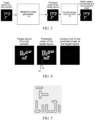
- FIG. 3 is a schematic diagram of a model training process according to an embodiment of the present disclosure.
- a pre-defined layout of a chip sample in the training sample is inputted into a mask generation model 10.
- the mask generation model 10 outputs a predicted mask of the pre-defined layout of the chip sample, and then the predicted mask of the pre-defined layout is inputted into a photolithography physical model 20 to output a wafer pattern corresponding to the predicted mask of the pre-defined layout.
- the photolithography physical model is a photolithography physical model with a process parameter being considered.
- the pre-defined layout of the chip sample, the predicted mask of the pre-defined layout of the chip sample, and the wafer pattern corresponding to the predicted mask of the pre-defined layout of the chip sample in each training sample in the set of training samples may be obtained.
- S104 Determine complexity of the predicted mask of the pre-defined layout based on a sum of perimeters of a plurality of graphics included in the pre-defined layout of the chip sample and a perimeter of the predicted mask of the pre-defined layout.
- low complexity of the mask may be defined as that the mask is substantially free of micro structures such as holes, isolated items, and sawteeth. Therefore, the complexity of the predicted mask of the pre-defined layout may be determined based on the sum of the perimeters of the plurality of graphics included in the pre-defined layout of the chip sample and the perimeter of the predicted mask of the pre-defined layout.
- the complexity of the predicted mask of the pre-defined layout needs to be considered when a model parameter is adjusted during model training. Therefore, the complexity of the predicted mask of the pre-defined layout needs to be first determined. For ease of description, FIG.
- FIG. 4 is a schematic diagram of a pre-defined layout of a chip sample, a predicted mask of the pre-defined layout of the chip sample, and a contour line of the predicted mask of the pre-defined layout of the chip sample.
- the pre-defined layout of the chip sample, the predicted mask of the pre-defined layout of the chip sample, and the contour line of the predicted mask of the pre-defined layout of the chip sample are sequentially from left to right.
- the predicted mask of the pre-defined layout of the chip sample includes a hole and an isolated item.
- One hole 30 and one isolated item 40 are schematically marked in FIG. 4 .
- the predicted mask of the pre-defined layout shown in FIG. 4 further includes another isolated item.
- the sum of the perimeters of the plurality of graphics included in the pre-defined layout refers to a sum of perimeters of all the graphics included in the pre-defined layout.
- the perimeter of the predicted mask of the pre-defined layout refers to a sum of lengths of contour lines of the predicted mask of the pre-defined layout. That the sum of the perimeters of the plurality of graphics included in the pre-defined layout is closer to the perimeter of the predicted mask of the pre-defined layout indicates that the complexity of the predicted mask of the pre-defined layout is lower. On the contrary, the complexity of the predicted mask of the pre-defined layout is higher.
- S104 may specifically be as follows:
- White represents a light-transmitting region
- black represents a light-shielding region or a light-blocking region.
- a pixel value of white is 1, and a pixel value of black is 0. Therefore, summation of the contour line of the predicted mask of the pre-defined layout is the perimeter of the predicted mask Mask pred of the pre-defined layout.
- the complexity of the predicted mask of the pre-defined layout is lower, that is, L C is smaller.
- higher complexity of the predicted mask of the pre-defined layout indicates that L C is larger.
- the complexity of the mask depends only on a shape of the pre-defined layout and a shape of the mask, is independent of a specific optical physical model, and may be used in another optical physical model.
- the chip layout is first obtained, and the chip layout is inputted into the trained mask generation model, to output the mask corresponding to the chip layout.
- the mask corresponding to the chip layout is inputted into the photolithography physical model, to obtain the wafer pattern corresponding to the predicted mask of the pre-defined layout.
- the photolithography physical model herein may be any photolithography physical model, and is not limited to a photolithography physical model used during training of the mask generation model, while in the related art, only the photolithography physical model used during training of the mask generation model can be used, so that transferability of the mask generation model in the embodiments of the present disclosure is high.
- S105 Adjust a parameter of the mask generation model based on the pre-defined layout of the chip sample, the wafer pattern corresponding to the predicted mask of the pre-defined layout, the mask of the pre-defined layout, the predicted mask of the pre-defined layout, and the complexity of the predicted mask of the pre-defined layout until a training stop condition is met, to obtain a trained mask generation model.
- the parameters such as the weights of a neural network
- the parameters must be adjusted so that the model can learn the mapping relationship from the chip layout (pre-defined layout) to mask design. This process is carried out by comparing the predicted mask and the wafer pattern generated by it through the photolithography physical model with the actual mask of the given chip layout and the desired wafer pattern.
- the parameters are adjusted to: ensure that the predicted mask generated by the model is as close as possible to the actual mask of the given chip layout, maintaining the precision of the mask design, make the wafer pattern generated from the predicted mask through the photolithography physical model as close as possible to the ideal pattern of the target chip layout on the wafer, ensuring the accuracy of the lithography process, keep the complexity of the predicted mask at a relatively low level to reduce the difficulty and cost of mask manufacturing while guaranteeing the quality of the lithographic patterns.
- This series of adjustments and comparisons continues until a pre-defined training stop condition is met (such as reaching a predetermined number of training iterations or the loss function value falling below a preset threshold), at which point the training stops.
- the goal is to obtain a trained mask generation model that can produce low-complexity masks when later applied to chip layout mask design, supporting efficient lithography and chip fabrication with high-quality masks.
- the parameter of the mask generation model may be adjusted based on the pre-defined layout of each chip sample in the set of training samples, the wafer pattern corresponding to the predicted mask of the pre-defined layout of the chip sample, the mask of the pre-defined layout of the chip sample, the predicted mask of the pre-defined layout of the chip sample, and the complexity of the predicted mask of the pre-defined layout of the chip sample that are obtained in a current iteration process, until the training stop condition is met.
- the parameter of the mask generation model may be adjusted through gradient descent, so that the wafer pattern corresponding to the predicted mask of the pre-defined layout of the chip sample and the pre-defined layout of the chip sample are as close as possible, the mask of the pre-defined layout of the chip sample and the predicted mask of the pre-defined layout of the chip sample are as close as possible, and the complexity of the predicted mask of the pre-defined layout of the chip sample is reduced (for example, the complexity of the predicted mask is less than a preset threshold), to finally obtain the trained mask generation model.
- the mask may also be referred to as a photomask.
- the concepts of the two are the same.
- adjusting the parameter of the mask generation model based on the pre-defined layout of the chip sample, the wafer pattern corresponding to the predicted mask of the pre-defined layout, the mask of the pre-defined layout, the predicted mask of the pre-defined layout, and the complexity of the predicted mask of the pre-defined layout may specifically be:
- S1053 may specifically be as follows: obtain the composite loss function by calculation based on a sum of a product of a first parameter and the first loss function, a product of a second parameter and the complexity of the predicted mask of the pre-defined layout, and the second loss function.
- the composite loss function L calculated based on the sum of the product of the first parameter and the first loss function, the product of the second parameter and the complexity of the predicted mask of the pre-defined layout, and the second loss function may specifically be represented by the following Formula (2):
- L Mask pred ⁇ Mask 2 + ⁇ ⁇ L total + ⁇ ⁇ L c
- Mask represents the mask of the pre-defined layout
- Mask pred represents the predicted mask of the pre-defined layout
- L total represents the first loss function
- 2 represents the second loss function
- ⁇ is the first parameter
- ⁇ represents the second parameter
- ⁇ and ⁇ are adjustable parameters
- L C represents the complexity of the predicted mask of the pre-defined layout, which may specifically be obtained through calculation by using the foregoing Formula (1).
- ⁇ (h ⁇ ) represents an out of focus process parameter distribution function
- ⁇ (h ⁇ ) exp ⁇ h ⁇ 2 2 ⁇ h 2
- h ⁇ represents that a wafer is located at a distance h from a focal plane of a photolithography machine
- ⁇ h represents distribution function widening.
- ⁇ is a subscript of h
- U represents that an array length of h ⁇ , which may be 3, and ⁇ h may be 80
- ⁇ (t q ) represents an exposure dose deviation process parameter distribution function
- ⁇ t q exp ⁇ t q 2 2 ⁇ q 2
- t q represents an exposure dose deviation of the photolithography machine
- ⁇ q represents distribution function widening.
- q is a subscript of t
- Q represents an array length of t q , which may be 3 herein, and ⁇ q may be 0.1
- ⁇ , ⁇ , and ⁇ represent adjustable coefficients for balancing relative values of the loss functions, which may be, for example, 0.025, 0.06, and 2 respectively.
- R D represents a discrete regular term
- R TV represents a total variation regular term
- L MEPE represents a modified edge placement error loss function
- L Aerial represents an imaging error.
- L represents a sum of perimeters of all graphics in a pre-defined layout
- a dimension of the imaging error is a unit of length, and is consistent with a dimension of a chip node size.
- ⁇ is an adjustable parameter, which may be, for example, 2.
- h ⁇ and t q have the same meaning as those in the foregoing Formula (3).
- the wafer pattern Z corresponding to the predicted mask of the pre-defined layout is obtained through calculation by using a photolithography physical model.
- the photolithography physical model may be, for example, a Hopkins diffraction photolithography physical model of a partially coherent imaging system.
- the model obtains a light intensity distribution I(x, y; h ⁇ ) imaged on the wafer, and the light intensity distribution is obtained by convolving a mask M and a photolithography system kernel function h.
- the kernel function is obtained by performing singular value decomposition on a cross transfer coefficient of the photolithography system (for example, a 193 nm annular light source).
- An imaging pattern on a wafer (namely, the wafer pattern Z) is obtained by transforming the light intensity distribution I(x, y; h ⁇ ) through a sigmoid function.
- Pixel values of the mask obtained through optimization are in a continuous distribution between 0 and 1, and there is an error between the continuous distribution and a discrete distribution of the binary mask.
- L MEPE L Aerial ⁇ MEPE + ⁇ R D ⁇ MEPE + ⁇ R TV ⁇ MEPE
- L Aerial-MEPE represents an imaging edge placement error
- R D-MEPE represents a discrete regular term of an edge placement error
- R TV-MEPE represents a total variation regular term of the edge placement error
- FIG. 5 is a schematic diagram of a modified edge placement error. As shown in FIG.
- a matrix formed by black short line data points represents the modified edge placement error
- a length of the black short line represents a length of the edge placement error
- a plurality of graphics formed by black long lines together form the pre-defined layout of the chip sample
- ⁇ represents multiplication of corresponding elements of the matrix formed by the black short line data points.
- S1054 Adjust the parameter of the mask generation model through a gradient descent algorithm based on the composite loss function until the training stop condition is met.
- Mask represents a mask of a pre-defined layout
- Mask pred represents a predicted mask of a pre-defined layout
- L total represents a first loss function
- 2 represents a second loss function
- ⁇ is a first parameter
- ⁇ represents a second parameter
- ⁇ and ⁇ are adjustable parameters
- L c represents complexity of the predicted mask of the pre-defined layout, which may specifically be obtained through calculation by using the foregoing Formula (1).
- the first loss function is obtained through calculation based on the pre-defined layout of the chip sample and the wafer pattern corresponding to the predicted mask of the pre-defined layout
- the second loss function is obtained through calculation based on the mask of the pre-defined layout and the predicted mask of the pre-defined layout.
- the composite loss function includes three parts. A damage function is minimized by the gradient descent algorithm, so that the parameter of the mask generation model is continuously adjusted, and the wafer pattern corresponding to the predicted mask of the pre-defined layout of the chip sample and the pre-defined layout of the chip sample are as close as possible, and the mask of the pre-defined layout of the chip sample and the predicted mask of the pre-defined layout of the chip sample are as close as possible.
- the complexity of the predicted mask of the pre-defined layout of the chip sample is reduced (for example, the complexity of the predicted mask is less than a preset threshold).
- S1054 may specifically be as follows:
- S10541 Obtain a gradient of the composite loss function by calculation based on the parameter of the mask generation model in a current iteration process.
- S10542 Adjust the parameter of the mask generation model based on an optimization direction and an optimization step size of the gradient descent algorithm until the training stop condition is met.
- the training stop condition may be that a preset number of iterative training times is reached, or may be that a gradient of the composite loss function reaches a preset value, or another training stop condition. This is not limited in this embodiment.
- the mask generation model in this embodiment may be a pre-trained model.
- the method in this embodiment may further include:
- S106 Obtain a set of sample data, each sample data in the set of sample data comprising a pre-defined layout of a chip sample and a mask of the pre-defined layout of the chip sample.
- obtaining a set of sample data may specifically be: the set of sample data is obtained by using a pixelation-based inverse lithography method.
- obtaining the set of training samples may specifically be: selecting a preset number of pieces of sample data from the set of sample data, and forming the set of training samples using the preset number of pieces of sample data.
- the mask generation model is pre-trained.
- a process of pre-training the mask generation model herein may specifically be: obtaining a set of training samples, each training sample in the set of training samples comprising a pre-defined layout of a chip sample and a mask of the pre-defined layout, for at least one training sample in the set of training samples, using the pre-defined layout of the chip sample in the training sample as an input for a mask generation model to obtain a predicted mask of the pre-defined layout as an output; calculating a loss function based on the mask of the pre-defined layout of the chip sample and the predicted mask of the pre-defined layout of the chip sample; and adjusting a parameter of the mask generation model based on the loss function until a training stop condition is met, to obtain a trained mask generation model.
- pre-training is performed on the mask generation model, and a model parameter of the pre-trained mask generation model is used as an initial model parameter and then trained, so that the model parameter can be first imported, so that the calculation amount is reduced and a model converge is faster.
- the mask generation model in this embodiment may include an encoder and a decoder.
- the encoder includes a plurality of convolutional neural network layers
- the decoder includes a plurality of deconvolutional neural network layers.
- the set of training samples is first obtained, for at least one training sample in the set of training samples, the pre-defined layout of the chip sample in the training sample is inputted into the mask generation model to obtain the predicted mask of the pre-defined layout, and then the predicted mask of the pre-defined layout is inputted into the photolithography physical model to obtain the wafer pattern corresponding to the predicted mask of the pre-defined layout.
- Complexity of the predicted mask of the pre-defined layout is determined based on a sum of perimeters of a plurality of graphics included in the pre-defined layout of the chip sample and a perimeter of the predicted mask of the pre-defined layout.
- a parameter of the mask generation model is adjusted based on the pre-defined layout of the chip sample, the wafer pattern corresponding to the predicted mask of the pre-defined layout, the mask of the pre-defined layout, the predicted mask of the pre-defined layout, and the complexity of the predicted mask of the pre-defined layout until a training stop condition is met, to obtain a trained mask generation model.
- the model parameter is not only adjusted based on the pre-defined layout of the chip sample, the wafer pattern corresponding to the predicted mask of the pre-defined layout, the mask of the pre-defined layout, and the predicted mask of the pre-defined layout, but also adjusted based on the complexity of the predicted mask of the pre-defined layout.
- the complexity of the predicted mask of the pre-defined layout is determined based on the sum of perimeters of the plurality of graphics included in the pre-defined layout of the chip sample and the perimeter of the predicted mask of the pre-defined layout, the complexity of the predicted mask of the pre-defined layout depends only on shapes of the pre-defined layout and the predicted mask of the pre-defined layout. Therefore, the mask generation model obtained through training has high transferability, and a calculation amount in a model training process is low.
- the set of sample data may be obtained by using a pixelation-based inverse lithography method.
- a specific obtaining process is described in detail in the following embodiments.
- S202 Pre-train a deep learning mask generation model based on the set of sample data.
- the mask generation model is pre-trained.
- a process of pre-training the mask generation model herein may specifically be: obtaining a set of training samples, each training sample in the set of training samples comprising a pre-defined layout of a chip sample and a mask of the pre-defined layout, for at least one training sample in the set of training samples, using the pre-defined layout of the chip sample in the training sample as an input for a mask generation model to obtain a predicted mask of the pre-defined layout as an output; calculating a loss function based on the mask of the pre-defined layout of the chip sample and the predicted mask of the pre-defined layout of the chip sample; and adjusting a parameter of the mask generation model based on the loss function until a training stop condition is met, to obtain a trained mask generation model.
- the mask generation model herein may be a deep learning model. After pre-training is completed, a parameter of the pre-trained mask generation model may be obtained, which may specifically be a neuron weight parameter of the mask generation model.
- S203 Obtain a set of training samples, each training sample in the set of training samples comprising a pre-defined layout of a chip sample and a mask of the pre-defined layout of the chip sample.
- a neuron weight parameter of the pre-trained mask generation model is initialized as a to-be-trained mask generation model, that is, the neuron weight parameter of the pre-trained mask generation model is used as an initialized weight parameter of the to-be-trained mask generation model.
- the obtaining the set of training samples may be selecting a preset number of pieces of sample data from the set of sample data, and forming the set of training samples using the preset number of pieces of sample data.
- S204 For at least one training sample in the set of training samples, use a pre-defined layout of a chip sample in the training sample as an input of the mask generation model, to output a predicted mask of the pre-defined layout, and input the predicted mask of the pre-defined layout into a wafer pattern prediction model, which is a photolithography physical model, to output a wafer pattern corresponding to the predicted mask of the pre-defined layout.
- a wafer pattern prediction model which is a photolithography physical model
- the pre-defined layout of the chip sample, the predicted mask of the pre-defined layout of the chip sample, and the wafer pattern corresponding to the predicted mask of the pre-defined layout of the chip sample in each training sample in the set of training samples may be obtained.
- S205 Determine complexity of the predicted mask of the pre-defined layout based on a sum of perimeters of a plurality of graphics included in the pre-defined layout of the chip sample and a perimeter of the predicted mask of the pre-defined layout.
- obtain the complexity of the predicted mask of the pre-defined layout by calculation based on the result of dividing the perimeter of the predicted mask of the pre-defined layout by the sum of perimeters of the plurality of graphics L may specifically be represented by the foregoing Formula (1).
- S206 Adjust a parameter of the mask generation model based on the pre-defined layout of the chip sample, the wafer pattern corresponding to the predicted mask of the pre-defined layout, the mask of the pre-defined layout, the predicted mask of the pre-defined layout, and the complexity of the predicted mask of the pre-defined layout until a training stop condition is met, to obtain a trained mask generation model.
- adjust the parameter of the mask generation model based on the pre-defined layout of the chip sample, the wafer pattern corresponding to the predicted mask of the pre-defined layout, the mask of the pre-defined layout, the predicted mask of the pre-defined layout, and the complexity of the predicted mask of the pre-defined layout may specifically be:
- construct a composite loss function L based on the first loss function, the second loss function, and the complexity of the predicted mask of the pre-defined layout may specifically be represented by the foregoing Formula (2).
- L total can be represented by the foregoing Formula (3).
- the first loss function is obtained through calculation based on the pre-defined layout of the chip sample and the wafer pattern corresponding to the predicted mask of the pre-defined layout
- the second loss function is obtained through calculation based on the mask of the pre-defined layout and the predicted mask of the pre-defined layout.
- the composite loss function includes three parts. A damage function is minimized by the gradient descent algorithm, so that the parameter of the mask generation model is continuously adjusted, and the wafer pattern corresponding to the predicted mask of the pre-defined layout of the chip sample and the pre-defined layout of the chip sample are as close as possible, and the mask of the pre-defined layout of the chip sample and the predicted mask of the pre-defined layout of the chip sample are as close as possible.
- the complexity of the predicted mask of the pre-defined layout of the chip sample is reduced (for example, the complexity of the predicted mask is less than a preset threshold).
- S2064 may specifically be as follows: S20641: Calculate a gradient of the composite loss function based on the parameter of the mask generation model in a current iteration process.
- the pre-defined layout of the chip sample in the training sample is inputted into the mask generation model to obtain the predicted mask of the pre-defined layout, and then the predicted mask of the pre-defined layout is inputted into the photolithography physical model to obtain the wafer pattern corresponding to the predicted mask of the pre-defined layout.
- the complexity of the predicted mask of the pre-defined layout is determined based on the sum of the perimeters of the plurality of graphics included in the pre-defined layout of the chip sample and the perimeter of the predicted mask of the pre-defined layout, and the composite loss function is constructed based on the pre-defined layout of the chip sample, the wafer pattern corresponding to the predicted mask of the pre-defined layout, the mask of the pre-defined layout, the predicted mask of the pre-defined layout, and the complexity of the predicted mask of the pre-defined layout, to bring the wafer pattern corresponding to the predicted mask of the pre-defined layout closer to the pre-defined layout of the chip sample by gradient descent, so that the mask of the pre-defined layout of the chip sample is as close as possible to the predicted mask of the pre-defined layout of the chip sample, In addition, complexity of the predicted mask of the pre-defined layout of the chip sample is reduced.
- the complexity of the predicted mask of the pre-defined layout is determined based on the sum of the perimeters of the plurality of graphics included in the pre-defined layout of the chip sample and the perimeter of the predicted mask of the pre-defined layout, the complexity of the predicted mask of the pre-defined layout depends only on the pre-defined layout and a shape of the predicted mask of the pre-defined layout. Therefore, the mask generation model obtained through training has high transferability, and a calculation amount in a model training process is low.
- a method of obtaining the set of sample data may include: S1: Determine a loss function.
- the sigmoid function herein may also function as a filter to filter out micro complex structures (islands, hollows, sawteeth, and stretched items) in a generated mask, thereby increasing manufacturability of the mask.
- an optimization direction is the gradient ⁇ L total ⁇ M ⁇ of the loss function L total about the mask.
- an initial descent direction is ⁇ L total ⁇ M ⁇
- a subsequent descent direction retains the optimization direction of a previous step
- a conjugate gradient factor ⁇ k is automatically adjusted to avoid optimization stagnation.
- the mask is updated based on the optimization direction, specifically, the pixel value of the mask is updated.
- the updated pixel value of the mask may exceed 1 or be less than 0.
- the mask value may be fixed to between 0 and 1 through the sigmoid function.
- Updated mask M i + 1 M i + ⁇ k * ⁇ L ⁇ Mi , and M i is a mask before updating.
- S5 Repeat S3 and S4, and optimize a process until a preset number of iterative training times is reached or a gradient reaches an expected value.
- S3 and S4 are repeated, and the optimization process is repeated until a preset number of iterative training times is reached.
- the preset number of iterative training times is 1000.
- the optimization process is stopped.
- S3 and S4 are repeated, and the optimization process is stopped until the gradient reaches an expected value.
- the expected value of the gradient may be preset.
- the optimized mask is the mask of the pre-defined layout.
- the mask of the pre-defined layout of the chip sample is obtained through the foregoing method.
- a widely used public photolithography mask data set is selected in this embodiment.
- a total of 10271 chip layouts and corresponding masks are included in the two data sets.
- the chip layout is generated meeting a 32 nm process node and a specific design rule.
- the mask in the photolithography mask data set is obtained through the foregoing pixelation-based inverse lithography method.
- the mask generation model training is performed based on the method for training a mask generation model provided in the embodiments of the present disclosure, to obtain the mask generation model.
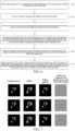
- FIG. 7 is a schematic diagram of a comparison of mask effects according to an embodiment of the present disclosure.
- four columns in FIG. 7 sequentially represent a pre-defined layout, a mask of the pre-defined layout, a wafer pattern, and a difference between the pre-defined layout and the wafer pattern.
- a first behavior uses a mask, a wafer pattern, and a difference between the pre-defined layout and the wafer pattern that are generated by the mask generation model obtained by the method for training a mask generation model provided in this embodiment of the present disclosure.
- a second behavior uses a mask, a wafer pattern, and a difference between the pre-defined layout and the wafer pattern that are generated by an existing mask optimization algorithm.
- a third behavior uses a mask, a wafer pattern, and a difference between a pre-defined layout and a wafer pattern that are generated by an existing inverse lithography mask optimization algorithm.
- FIG. 8 is a schematic diagram of a comparison of mask effects according to an embodiment of the present disclosure.
- four columns in FIG. 8 sequentially represent a pre-defined layout, a mask of the pre-defined layout, a wafer pattern, and a difference between the pre-defined layout and the wafer pattern.
- a first behavior uses a mask, a wafer pattern, and a difference between the pre-defined layout and the wafer pattern that are generated by the mask generation model obtained by the method for training a mask generation model provided in this embodiment of the present disclosure.
- a second behavior uses a mask, a wafer pattern, and a difference between the pre-defined layout and the wafer pattern that are generated by an existing mask optimization algorithm.
- a third behavior uses a mask, a wafer pattern, and a difference between a pre-defined layout and a wafer pattern that are generated by an existing inverse lithography mask optimization algorithm.
- the mask generation model in this embodiment may include an encoder and a decoder.
- the encoder includes a plurality of convolutional neural network layers
- the decoder includes a plurality of deconvolutional neural network layers.
- the encoder includes 8 convolutional neural network layers
- the decoder includes eight deconvolutional neural network layers.
- the eight convolutional layers are respectively formed by eight 3 ⁇ 3 filters, 16 3 ⁇ 3 filters, 32 3 ⁇ 3 filters, 64 3 ⁇ 3 filters, 128 3 ⁇ 3 filters, 256 3 ⁇ 3 filters, 512 3 ⁇ 3 filters, and 1024 3 ⁇ 3 filters.
- a batch normalization layer is established after each convolutional layer and a subsequent activation function uses a modified linear unit (ReLU).
- ReLU modified linear unit
- a final output with dimensions (1, 1, 1024) is used as an input of the decoder.
- the first seven deconvolutional layers are respectively formed by 1024 3 ⁇ 3 filters, 512 3 ⁇ 3 filters, 256 3 ⁇ 3 filters, 128 3 ⁇ 3 filters, 64 3 ⁇ 3 filters, 32 3 ⁇ 3 filters, and 16 3 ⁇ 3 filters sequentially.
- a batch normalization layer is established and a Leaky modified linear unit (Leaky-ReLU) is used as a subsequent activation function.
- Leaky-ReLU Leaky modified linear unit
- a deconvolutional neural network layer including eight 3 ⁇ 3 filters and a sigmoid activation function gives a predicted mask with dimensions (256, 256, 1) and values 0 to 1, and then binarization processing is performed on the mask to obtain a final mask.
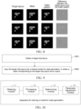
- FIG. 9 is a flowchart of a method for mask generation according to an embodiment of the present disclosure.
- An execution body of the method may be a server. As shown in FIG. 9 , the method may include:
- the mask generation model is obtained through training based on the method in the embodiment shown in FIG. 2 or FIG. 6 .
- a mask with low complexity can be generated through the mask generation model, so that a mask with high quality can be provided for a subsequent chip photolithography process, thereby reducing calculation time and manufacturing costs of the mask.
- FIG. 10 is a schematic structural diagram of an apparatus for training a mask generation model according to an embodiment of the present disclosure.
- the apparatus may include: an obtaining module 11, a processing module 12, a determining module 13, and a parameter adjustment module 14.
- the obtaining module 11 is configured to obtain a set of training samples, each training sample in the set of training samples comprising a pre-defined layout of a chip sample and a mask of the pre-defined layout.
- the processing module 12 is configured to use, for at least one training sample in the set of training samples, a pre-defined layout of a chip sample in the training sample as an input for a mask generation model.
- the processing module 12 is further configured to obtain a predicted mask of the pre-defined layout as an output, and input the predicted mask of the pre-defined layout into a wafer pattern prediction model, which is a photolithography physical model, to obtain a wafer pattern corresponding to the predicted mask of the pre-defined layout.
- a wafer pattern prediction model which is a photolithography physical model
- the determining module 13 is configured to determine complexity of the predicted mask of the pre-defined layout based on a sum of perimeters of a plurality of graphics included in the pre-defined layout of the chip sample and a perimeter of the predicted mask of the pre-defined layout.
- the parameter adjustment module 14 is configured to adjust a parameter of the mask generation model based on the pre-defined layout of the chip sample, the wafer pattern corresponding to the predicted mask of the pre-defined layout, the mask of the pre-defined layout, the predicted mask of the pre-defined layout, and the complexity of the predicted mask of the pre-defined layout until a training stop condition is met, to obtain a trained mask generation model.
- the determining module 13 is configured to: calculate contour lines of the predicted mask of the pre-defined layout based on a sum of a square of a first-order derivative of the predicted mask of the pre-defined layout in an x direction and a square of a first-order derivative of the predicted mask of the pre-defined layout in a y direction;
- the parameter adjustment module 14 is configured to:
- the parameter adjustment module 14 is further configured to: obtain the composite loss function by calculation based on a sum of a product of a first parameter and the first loss function, a product of a second parameter and the complexity of the predicted mask of the pre-defined layout, and the second loss function.
- the parameter adjustment module 14 is further configured to:
- the mask generation model is a pre-trained model
- the obtaining module 11 is further configured to:
- the obtaining module 11 is further configured to:
- the mask generation model includes an encoder and a decoder.
- the encoder includes a plurality of convolutional neural network layers
- the decoder includes a plurality of deconvolutional neural network layers.
- FIG. 11 is a schematic structural diagram of an apparatus for mask generation according to an embodiment of the present disclosure. As shown in FIG. 11 , the apparatus may include: an obtaining module 21 and a processing module 22.
- the obtaining module 21 is configured to obtain a chip layout.
- the processing module 22 is configured to input the chip layout into a trained mask generation model, to obtain a mask corresponding to the chip layout as an output, the mask generation model being obtained through training according to the method in the embodiment shown in FIG. 1 .
- Apparatus embodiments and method embodiments may correspond to each other.
- details are not described herein again.
- the apparatus for training a mask generation model shown in FIG. 10 or the apparatus for mask generation shown in FIG. 11 may perform a method embodiment corresponding to the terminal device or the server, and the foregoing and other operations and/or functions of the modules in the apparatus are respectively intended to implement the method embodiment corresponding to the terminal device or the server.
- the apparatus for training a mask generation model shown in FIG. 10 or the apparatus for mask generation shown in FIG. 11 may perform a method embodiment corresponding to the terminal device or the server, and the foregoing and other operations and/or functions of the modules in the apparatus are respectively intended to implement the method embodiment corresponding to the terminal device or the server.
- details are not described herein again.
- the apparatus for training a mask generation model and the apparatus for mask generation of the embodiments of the present disclosure are described above with reference to the accompanying drawings from a perspective of a functional module.
- the functional module may be implemented in hardware form, or may be implemented in software form of instructions, or may be implemented through a combination of hardware and software modules.
- operations of the method embodiments in the embodiments of the present disclosure may be completed by instructions in the form of hardware integrated logic circuits and/or software in the processor, and operations of the methods disclosed with reference to the embodiments of the present disclosure may be directly performed and completed by using a hardware decoding processor, or may be performed and completed by using a combination of hardware and software modules in the decoding processor.
- the software module may be located in a mature storage medium in the art, such as a random access memory, a flash memory, a read-only memory, a programmable read-only memory, an electrically-erasable programmable memory, and a register.
- the storage medium is located in the memory.
- the processor reads information in the memory and completes the operations of the foregoing method embodiments in combination with hardware thereof.
- FIG. 12 is a schematic block diagram of a computer device 300 according to an embodiment of the present disclosure.
- the computer device 300 may include: a memory 310 and a processor 320.
- the memory 310 is configured to store a computer program and transmit program code to the processor 320.
- the processor 320 may invoke and run the computer program from the memory 310 to implement the method in the embodiments of the present disclosure.
- the processor 320 may be configured to perform the foregoing method embodiment based on instructions in the computer program.
- the processor 320 may include, but is not limited to: a general processor, a digital signal processor (DSP), an application specific integrated circuit (ASIC), a field programmable gate array (FPGA), another programmable logic device, a discrete gate, a transistor logic device, a discrete hardware component, or the like.
- DSP digital signal processor
- ASIC application specific integrated circuit
- FPGA field programmable gate array
- the memory 310 includes, but is not limited to: a non-volatile memory and/or a volatile memory.
- the non-volatile memory may be a read-only memory (ROM), a programmable read-only memory (PROM), an erasable programmable read-only memory (EPROM), an electrically erasable programmable read-only memory (EEPROM), or a flash memory.
- the volatile memory may be a random access memory (RAM) that is used as an external cache.
- RAMs may be used, for example, a static random access memory (SRAM), a dynamic random access memory (DRAM), a synchronous dynamic random access memory (SDRAM), a double data rate synchronous dynamic random access memory (DDR SDRAM), an enhanced synchronous dynamic random access memory (ESDRAM), a synchronous link dynamic random access memory (SLDRAM), and a direct rambus dynamic random access memory (DR RAM).
- SRAM static random access memory
- DRAM dynamic random access memory
- SDRAM synchronous dynamic random access memory
- DDR SDRAM double data rate synchronous dynamic random access memory
- ESDRAM enhanced synchronous dynamic random access memory
- SLDRAM synchronous link dynamic random access memory
- DR RAM direct rambus dynamic random access memory
- the computer program may be divided into one or more modules, and the one or more modules are stored in the memory 310 and executed by the processor 320 to perform the methods provided in the embodiments of the present disclosure.
- the one or more modules may be a series of computer program instruction segments capable of performing a particular function, and the instruction segments are configured for describing the execution of the computer program in the electronic device.
- the computer device may further include: a transceiver 330.
- the transceiver 330 may be connected to the processor 320 or the memory 310.
- the processor 320 may control the transceiver 330 to communicate with another device, and specifically, may send information or data to another device or receive information or data sent by another device.
- the transceiver 330 may include a transmitter and a receiver.
- the transceiver 330 may further include an antenna, and a number of antennas may be one or more.
- the bus system further includes a power bus, a control bus, and a status signal bus.
- An embodiment of the present disclosure further provides a computer storage medium, having a computer program stored therein.
- the computer program When the computer program is executed by a computer, the computer is enabled to perform the method according to the foregoing method embodiments.
- an embodiment of the present disclosure further provides a computer program product including instructions. When the instructions executed by a computer, the computer is caused to perform the method according to the foregoing method embodiments.
- the computer instructions may be transmitted from one website, computer, server or data center to another website, computer, server or data center in a wired (for example, a coaxial cable, an optical fiber or a digital subscriber line (DSL)) or wireless (for example, infrared, wireless or microwave) manner.
- the computer-readable storage medium may be any usable medium accessible by the computer, or a data storage device, for example, a server or a data center, integrating one or more usable media.
- the available medium may be a magnetic medium (such as a floppy disk, a hard disk, or a magnetic tape), an optical medium (such as a digital video disc (DVD)), a semiconductor medium (such as a solid state disk (SSD)) or the like.
- modules and algorithm steps may be implemented by electronic hardware or a combination of computer software and electronic hardware. Whether the functions are performed by hardware or software depends on particular applications and design constraint conditions of the technical solutions. A person skilled in the art may use different methods to implement the described functions for each particular application, but it is not to be considered that the implementation goes beyond the scope of the embodiments of the present disclosure.
- the disclosed system, apparatus, and method may be implemented in other manners.
- the described apparatus embodiment is merely exemplary.
- the module division is merely logical function division and may be other division in actual implementation.
- a plurality of modules or components may be combined or integrated into another system, or some features may be ignored or not performed.
- the displayed or discussed mutual couplings or direct couplings or communication connections may be implemented by using some interfaces.
- the indirect couplings or communication connections between the apparatuses or modules may be implemented in electronic, mechanical, or other forms.
- modules described as separate parts may or may not be physically separate, and parts displayed as modules may or may not be physical modules, may be located in one position, or may be distributed on a plurality of network units. Some or all of the modules may be selected according to actual requirements to implement the objectives of the solutions of the embodiments. For example, functional modules in the embodiments of the present disclosure may be integrated into one processing module, or each of the modules may exist alone physically, or two or more modules may be integrated into one module.
Landscapes
- Engineering & Computer Science (AREA)
- Physics & Mathematics (AREA)
- Theoretical Computer Science (AREA)
- General Physics & Mathematics (AREA)
- Evolutionary Computation (AREA)
- Health & Medical Sciences (AREA)
- Artificial Intelligence (AREA)
- Computing Systems (AREA)
- General Engineering & Computer Science (AREA)
- General Health & Medical Sciences (AREA)
- Software Systems (AREA)
- Computer Hardware Design (AREA)
- Data Mining & Analysis (AREA)
- Molecular Biology (AREA)
- Life Sciences & Earth Sciences (AREA)
- Biomedical Technology (AREA)
- Biophysics (AREA)
- Computational Linguistics (AREA)
- Mathematical Physics (AREA)
- Multimedia (AREA)
- Databases & Information Systems (AREA)
- Medical Informatics (AREA)
- Computer Vision & Pattern Recognition (AREA)
- Geometry (AREA)
- Architecture (AREA)
- Preparing Plates And Mask In Photomechanical Process (AREA)
Abstract
Description
- The present disclosure claims priority to
Chinese Patent Application No. 202311005424.2, filed with the China National Intellectual Property Administration on August 10, 2023 - Embodiments of the present disclosure relate to the field of artificial intelligence (AI) technologies, and in particular, to a method for training a mask generation model, a method and an apparatus for mask generation, and a storage medium.
- A photolithography process is referred to as a process to transfer a geometric figure on a mask to a photoresist on a surface of a wafer. A photoresist processing device is used to spin coating the photoresist on the surface of the wafer. After step-and-repeat exposure and development processing, a required pattern is formed on the wafer. As a feature size of a very large-scale integrated circuit continues to shorten and is below a light source wavelength used in the photolithography process, an interference phenomenon and a diffraction phenomenon are clearly apparent. As a result, a pattern formed by exposure on a wafer through a mask differs greatly from a required pattern, which seriously affects chip performance, throughput, and yield. To resolve this problem, deep learning technologies are applied to various fields of chip design and manufacturing. To ensure high quality of the mask, low complexity of a generated mask needs to be ensured.
- In the related art, one method is to optimize the generated mask by using a deep learning algorithm, and another method is to generate the mask by using a pixelation-based inverse lithography technology. However, masks generated by the two methods have high complexity and are difficult to be used in large-scale integrated circuit layout optimization.
- Embodiments of the present disclosure provide a method for training a mask generation model, a method and an apparatus for mask generation, and a storage medium, which can reduce complexity of a mask.
- According to a first aspect, an embodiment of the present disclosure provides a method for training a mask generation model, including:
- obtaining a set of training samples, each training sample in the set of training samples comprising a pre-defined layout of a chip sample and a mask of the pre-defined layout;
- using, for at least one training sample in the set of training samples, a pre-defined layout of a chip sample in the training sample as an input for a mask generation model, to obtain a predicted mask of the pre-defined layout as an output; inputting the predicted mask of the pre-defined layout into a wafer pattern prediction model, which is a photolithography physical model, to obtain a wafer pattern corresponding to the predicted mask of the pre-defined layout;
- determining complexity of the predicted mask of the pre-defined layout based on a sum of perimeters of a plurality of graphics included in the pre-defined layout of the chip sample and a perimeter of the predicted mask of the pre-defined layout; and
- adjusting a parameter of the mask generation model based on the pre-defined layout of the chip sample, the wafer pattern corresponding to the predicted mask of the pre-defined layout, the mask of the pre-defined layout, the predicted mask of the pre-defined layout, and the complexity of the predicted mask of the pre-defined layout until a training stop condition is met, to obtain a trained mask generation model.
- According to a second aspect, an embodiment of the present disclosure provides a method for mask generation, including:
- obtaining a chip layout; and
- inputting the chip layout into a trained mask generation model to obtain a mask corresponding to the chip layout as an output, the mask generation model being obtained through training according to the method described in the first aspect.
- According to a third aspect, an embodiment of the present disclosure provides an apparatus for training a mask generation model, including:
- an obtaining module, configured to obtain a set of training samples, each training sample in the set of training samples comprising a pre-defined layout of a chip sample and a mask of the pre-defined layout;
- a processing module, configured to use, for at least one training sample in the set of training samples, a pre-defined layout of a chip sample in the training sample as an input for a mask generation model, to obtain a predicted mask of the pre-defined layout as an output,
- the processing module being further configured to input the predicted mask of the pre-defined layout into a wafer pattern prediction model, which is a photolithography physical model, to obtain a wafer pattern corresponding to the predicted mask of the pre-defined layout;
- a determining module, configured to determine complexity of the predicted mask of the pre-defined layout based on a sum of perimeters of a plurality of graphics included in the pre-defined layout of the chip sample and a perimeter of the predicted mask of the pre-defined layout; and
- a parameter adjustment module, configured to adjust a parameter of the mask generation model based on the pre-defined layout of the chip sample, the wafer pattern corresponding to the predicted mask of the pre-defined layout, the mask of the pre-defined layout, the predicted mask of the pre-defined layout, and the complexity of the predicted mask of the pre-defined layout until a training stop condition is met, to obtain a trained mask generation model.
- According to a fourth aspect, an embodiment of the present disclosure provides an apparatus for mask generation, including:
- an obtaining module, configured to obtain a chip layout; and
- a processing module, configured to input the chip layout into a trained mask generation model to obtain a mask corresponding to the chip layout as an output, the mask generation model being obtained through training according to the method described in the first aspect.
- According to a fifth aspect, an embodiment of the present disclosure provides a computer device, including: a processor and a memory, the memory being configured to store a computer program, and the processor being configured to invoke and run the computer program stored in the memory to perform the method described in the first aspect or the second aspect.
- According to a sixth aspect, an embodiment of the present disclosure provides a computer-readable storage medium, including instructions that, when run on a computer program, cause the computer to perform the method described in the first aspect or the second aspect.
- According to a seventh aspect, an embodiment of the present disclosure provides a computer program product including instructions. When the instructions are run on a computer, the computer is enabled to perform the method described in the first aspect or the second aspect.
- In summary, in the embodiments of the present disclosure, a set of training samples is first obtained, for at least one training sample in the set of training samples, a pre-defined layout of a chip sample in the training sample is inputted into a mask generation model to obtain a predicted mask of the pre-defined layout as an output, and then the predicted mask of the pre-defined layout is inputted into a photolithography physical model to obtain a wafer pattern corresponding to the predicted mask of the pre-defined layout. Complexity of the predicted mask of the pre-defined layout is determined based on a sum of perimeters of a plurality of graphics included in the pre-defined layout of the chip sample and a perimeter of the predicted mask of the pre-defined layout. Then, a parameter of the mask generation model is adjusted based on the pre-defined layout of the chip sample, the wafer pattern corresponding to the predicted mask of the pre-defined layout, the mask of the pre-defined layout, the predicted mask of the pre-defined layout, and the complexity of the predicted mask of the pre-defined layout until a training stop condition is met, to obtain a trained mask generation model. In this way, when a model parameter of the mask generation model is adjusted, the model parameter is not only adjusted based on the pre-defined layout of the chip sample, the wafer pattern corresponding to the predicted mask of the pre-defined layout, the mask of the pre-defined layout, and the predicted mask of the pre-defined layout, but also adjusted based on the complexity of the predicted mask of the pre-defined layout. Therefore, complexity of the mask generated by the mask generation model can be reduced. In addition, since the complexity of the predicted mask of the pre-defined layout is determined based on the sum of perimeters of the plurality of graphics included in the pre-defined layout of the chip sample and the perimeter of the predicted mask of the pre-defined layout, the complexity of the predicted mask of the pre-defined layout depends only on shapes of the pre-defined layout and the predicted mask of the pre-defined layout. Therefore, the mask generation model obtained through training has high transferability, and a calculation amount in a model training process is low.
- Further, in the embodiments of the present disclosure, the mask generation model is pre-trained, and a model parameter of the pre-trained mask generation model is used as an initial model parameter for subsequent training, so that the calculation amount is reduced, and a model converge is faster.
-
-
FIG. 1 is a schematic diagram of an implementation scenario of a method for training a mask generation model and a method for mask generation according to an embodiment of the present disclosure. -
FIG. 2 is a flowchart of a method for training a mask generation model according to an embodiment of the present disclosure. -
FIG. 3 is a schematic diagram of a model training process according to an embodiment of the present disclosure. -
FIG. 4 is a schematic diagram of a pre-defined layout of a chip sample, a predicted mask of the pre-defined layout of the chip sample, and a contour line of the predicted mask of the pre-defined layout of the chip sample. -
FIG. 5 is a schematic diagram of a modified edge placement error. -
FIG. 6 is a flowchart of a method for training a mask generation model according to an embodiment of the present disclosure. -
FIG. 7 is a schematic diagram of a comparison of mask effects according to an embodiment of the present disclosure. -
FIG. 8 is a schematic diagram of a comparison of mask effects according to an embodiment of the present disclosure. -
FIG. 9 is a flowchart of a method for mask generation according to an embodiment of the present disclosure. -
FIG. 10 is a schematic structural diagram of an apparatus for training a mask generation model according to an embodiment of the present disclosure. -
FIG. 11 is a schematic structural diagram of an apparatus for mask generation according to an embodiment of the present disclosure. -
FIG. 12 is a schematic block diagram of acomputer device 300 according to an embodiment of the present disclosure. - The technical solutions in the embodiments of the present disclosure are clearly and completely described below with reference to accompanying drawings in the embodiments of the present disclosure. Apparently, the described embodiments are merely some rather than all of the embodiments of the present disclosure. All other embodiments obtained by a person of ordinary skill in the art based on embodiments in the embodiments of the present disclosure without creative efforts shall fall within the protection scope of the embodiments of the present disclosure.
- In the specification, claims, and accompanying drawings of the embodiments of the present disclosure, the terms "first", "second", and the like are intended to distinguish between similar objects but do not necessarily indicate a specific order or sequence. The data used in such a way is interchangeable in proper circumstances, so that embodiments in the embodiments of the present disclosure described herein can be implemented in other orders than the order illustrated or described herein. Moreover, the terms "include", "contain" and any other variants mean to cover the non-exclusive inclusion. For example, a process, method, system, product, or device that includes a list of operations or units is not necessarily limited to those operations or units, but may include other operations or units not expressly listed or inherent to such a process, method, product, or device.
- Before technical solutions of the embodiments of the present disclosure are described, relevant knowledge of the technical solutions of the embodiments of the present disclosure is explained below:
- 1. Artificial intelligence (AI): It is a theory, a method, a technology and an application system that uses a digital computer or a machine controlled by the digital computer to simulate, extend, and expand human intelligence, perceive the environment, acquire knowledge, and use knowledge to obtain an optimal result. In other words, the AI is a comprehensive technology in computer science. This technology attempts to understand the essence of intelligence and produce a new intelligent machine that can react in a manner similar to human intelligence. The AI is to study design principles and implementation methods of various intelligent machines, so that the machines have functions of perception, reasoning, and decision-making. The AI technology is a comprehensive discipline, relating to a wide range of fields, and involving both a hardware-level technology and a software-level technology. Basic AI technologies generally include technologies such as a sensor, a dedicated AI chip, cloud computing, distributed storage, a big data processing technology, an operating/interaction system, and electromechanical integration. AI software technologies mainly include several major directions such as a computer vision technology, a speech processing technology, a natural language processing technology, and machine learning/deep learning.
- 2. Machine learning (ML): It is a multi-field interdiscipline, and relates to a plurality of disciplines such as the probability theory, statistics, the approximation theory, convex analysis, and the algorithm complexity theory. The ML specializes in studying how a computer simulates or implements a human learning behavior to obtain new knowledge or skills, and reorganize an existing knowledge structure, so as to keep improving its performance. The ML is the core of the AI, is a basic way to make a computer intelligent, and is applied to various fields of AI. The ML and the deep learning generally include technologies such as an artificial neural network, a belief network, reinforcement learning, transfer learning, inductive learning, and learning from demonstrations.
- 3. Deep learning (DL): It is a branch of machine learning, and is an algorithm that attempts to perform high-level abstraction on data by using a plurality of processing layers including a complex structure or including a plurality of nonlinear transformations. The deep learning is learning an intrinsic rule and a representation level of training sample data. Information obtained in these learning processes greatly helps in the interpretation of data such as text, images, and sound. An ultimate objective of the deep learning is to enable a machine to have an analytical learning capability like a human being, and to recognize data such as text, images, and sound. The deep learning is a complex machine learning algorithm, and has effects in speech and image recognition that far exceed those in the previous related art.
- Neural network (NN): It is a deep learning model that simulates a structure and a function of a biological neural network in the field of machine learning and cognitive science.
- In the related art, complexity of a generated mask is high. To resolve this problem, in the embodiments of the present disclosure, when training a mask generation model, for at least one training sample in a set of training samples, a pre-defined layout of a chip sample in a training sample is inputted into the mask generation model, to obtain a predicted mask of the pre-defined layout as an output, and then the predicted mask of the pre-defined layout is inputted into a photolithography physical model to obtain a wafer pattern corresponding to the predicted mask of the pre-defined layout. The input to the mask generation model is the layout of the chip, typically represented as a 2D image, where each pixel value denotes the lithographic pattern information at the corresponding position. Each shape in the layout has clear dimensions and is used to define the locations of the components in the integrated circuit. The intermediate processing involves the model's internal computations, which usually include multiple convolutional layers and deconvolutional layers. The convolutional layers are responsible for feature extraction from the layout, such as edges, shapes, and local patterns, while the deconvolutional layers attempt to reconstruct the mask image based on these features. This process may also involve the application of activation functions, batch normalization layers, and skip connections to assist the model in learning more sophisticated and detailed mask generation patterns. The output of the mask generation model is the predicted mask image, also represented as a 2D image where each pixel value indicates whether light is allowed to pass at that location. The aim of mask generation is to ensure that when the lithographic process is performed, light can correctly form patterns on the wafer in accordance with the layout design. The output mask may require post-processing, such as binarization, to meet the requirements of the lithographic process. The photolithography physical model simulates the optical and chemical processes involved in photolithography to predict the final pattern printed on the wafer from a given mask. The input of the photolithography physical model may be: Mask pattern, the input to the photolithography physical model is usually a mask pattern, which is the design that needs to be transferred to the wafer. This mask pattern is typically represented as a binary or grayscale image where the transmittance of light is defined; Optical parameters, these include the wavelength of the light source, the numerical aperture of the lens, the coherence of the light source, and the distance between the mask and the wafer, among other factors that can affect the lithography process; Photoresist properties, the model also requires information about the photoresist properties, such as its sensitivity to light, the development process, and the profile it will take after the exposure and development steps; Process variables, variables such as focus, exposure dose, and other process parameters that influence the final pattern on the wafer. Intermediate processing of the photolithography physical model may be: Optical Simulation, the model performs optical simulation by calculating the light intensity distribution that would occur on the wafer surface given the mask pattern and the optical parameters. This involves using physics-based models that can account for diffraction, interference, and the interaction of light with the mask and photoresist; Chemical Simulation, After the optical simulation, there is a chemical simulation step to model the photoresist development process. This step transforms the light intensity distribution into a physical pattern on the wafer by simulating the chemical reactions that occur in the photoresist due to the exposure to light. Output of the photolithography physical model may be: Wafer Pattern, the output of the photolithography physical model is a simulated wafer pattern, which represents the final layout that would be printed on the wafer if the mask were to be used in an actual lithography process. This pattern can be compared to the desired layout to evaluate the quality of the mask and the lithography process.; Process Window, additionally, the model may output information about the process window, which describes the range of process variables (like focus and exposure dose) that result in an acceptable pattern on the wafer. A wide process window indicates a robust lithography process that is tolerant to variations in process parameters. The photolithography physical model's main goal is to accurately predict how the mask will behave in the photolithography process, allowing for the optimization of mask designs and process parameters to achieve the desired wafer patterns with high fidelity. The mask of the pre-defined layout represents the ideal mask design, optimized to reduce manufacturing costs, enhance the process window, and improve pattern fidelity. The mask of the pre-defined layout provides the correct solution for the training process. The predicted mask is a mask prediction output by the model when the layout as input, one of the objectives during model training is to make the predicted mask as close as possible to the mask of the pre-defined layout. Complexity of the predicted mask of the pre-defined layout is determined based on a sum of perimeters of a plurality of graphics included in the pre-defined layout of the chip sample and a perimeter of the predicted mask of the pre-defined layout. Then, a parameter of the mask generation model is adjusted based on the pre-defined layout of the chip sample, the wafer pattern corresponding to the predicted mask of the pre-defined layout, the mask of the pre-defined layout, the predicted mask of the pre-defined layout, and the complexity of the predicted mask of the pre-defined layout until a training stop condition is met, to obtain a trained mask generation model. In this way, in the embodiments of the present disclosure, when a model parameter of the mask generation model is adjusted, the model parameter is not only adjusted based on the pre-defined layout of the chip sample, the wafer pattern corresponding to the predicted mask of the pre-defined layout, the mask of the pre-defined layout, and the predicted mask of the pre-defined layout, but also adjusted based on the complexity of the predicted mask of the pre-defined layout. Therefore, complexity of the mask generated by the mask generation model can be reduced. In addition, since the complexity of the predicted mask of the pre-defined layout is determined based on the sum of perimeters of the plurality of graphics included in the pre-defined layout of the chip sample and the perimeter of the predicted mask of the pre-defined layout, the complexity of the predicted mask of the pre-defined layout depends only on shapes of the pre-defined layout and the predicted mask of the pre-defined layout. Therefore, the mask generation model obtained through training has high transferability, and a calculation amount in a model training process is low.
- The embodiments of the present disclosure may be applicable to various scenarios that require mask generation, for example, large-scale integrated circuit layout optimization. The method for training a mask generation model and the method for mask generation provided in the embodiments of the present disclosure may be loaded into computational lithography software. A chip mask manufacturer may obtain a mask corresponding to a chip layout by inputting the chip layout, and the mask has low complexity, so that a mask with high quality can be provided for a subsequent chip photolithography process. For example, specifically, a photolithography mask with low mask complexity may be provided, which significantly reduces calculation time and manufacturing costs of the mask, and increases a process window for generating the mask by the mask generation model. The process window may be understood as tolerances for an exposure amount and a focus deviation. The method for training a mask generation model and the method for mask generation provided in the embodiments of the present disclosure may also be extended to fields such as computer vision image generation.
- The application scenarios described below are merely configured for describing rather than limiting the embodiments of the present disclosure. During specific implementation, the technical solutions provided in the embodiments of the present disclosure are flexibly applicable according to an actual requirement.
- For example,
FIG. 1 is a schematic diagram of an implementation scenario of a method for training a mask generation model and a method for mask generation according to an embodiment of the present disclosure. As shown inFIG. 1 , the implementation scenario of the embodiments of the present disclosure involves aserver 1 and aterminal device 2. Theterminal device 2 may perform data communication on theserver 1 through a communication network. The communication network may be a wireless or wired network such as an intranet, the Internet, a global system of mobile communications (GSM), a wideband code division multiple access (WCDMA), a 4G network, a 5G network, Bluetooth, Wi-Fi, or a call network. - In some possible implementations, the
terminal device 2 refers to a type of device rich in human-computer interaction manners, capable of accessing the Internet, usually carrying various operating systems, and having a strong processing capability. The terminal device may be a terminal device such as a smartphone, a tablet computer, a portable notebook computer, or a desktop computer, or may be a phone watch, but is not limited thereto. In some embodiments of the present disclosure, various applications, for example, photolithography applications, are installed on theterminal device 2. - In some possible implementations, the
terminal device 2 includes, but is not limited to, a mobile phone, a computer, a smart speech interaction device, a smart household appliance, an in-vehicle terminal, or the like. - The
server 1 inFIG. 1 may be an independent physical server, or may be a server cluster or a distributed system formed by a plurality of physical servers, or may be a cloud server that provides a cloud computing service. This is not limited in the embodiments of the present disclosure. In the embodiments of the present disclosure, theserver 1 may be a backend server of an application installed in theterminal device 2. - In some possible implementations,
FIG. 1 exemplarily shows one terminal device and one server. Actually, terminal devices and servers of other numbers may be included. This is not limited in the embodiments of the present disclosure. - In some embodiments, when a mask corresponding to a chip layout needs to be obtained, the
server 1 may first train a mask generation model according to the method provided in the embodiments of the present disclosure. Specifically, the method may be as follows: obtaining a set of training samples, each training sample in the set of training samples comprising a pre-defined layout of a chip sample and a mask of the pre-defined layout, for at least one training sample in the set of training samples, using the pre-defined layout of the chip sample in the training sample as an input of the mask generation model to obtain a predicted mask of the pre-defined layout as an output; inputting the predicted mask of the pre-defined layout into a wafer pattern prediction model, which is a photolithography physical model to obtain a wafer pattern corresponding to the predicted mask of the pre-defined layout; determining complexity of the predicted mask of the pre-defined layout based on a sum of perimeters of a plurality of graphics included in the pre-defined layout of the chip sample and a perimeter of the predicted mask of the pre-defined layout; and adjusting a parameter of the mask generation model based on the pre-defined layout of the chip sample, the wafer pattern corresponding to the predicted mask of the pre-defined layout, the mask of the pre-defined layout, the predicted mask of the pre-defined layout, and the complexity of the predicted mask of the pre-defined layout until a training stop condition is met, to obtain a trained mask generation model. After the trained mask generation model is obtained, a user may upload the chip layout by using an application for generating the mask installed and run on theterminal device 2. Theterminal device 2 sends the uploaded chip layout to theserver 1. After obtaining the chip layout, theserver 1 inputs the chip layout into the trained mask generation model, and outputs a mask corresponding to the chip layout. Therefore, the mask corresponding to the chip layout can be obtained. In an embodiment, the training of the mask generation model may alternatively be performed by the terminal device, and the method for mask generation may also be performed by the terminal device. This is not limited in this embodiment. - The technical solution of the embodiments of the present disclosure is described in detail in the following:
FIG. 2 is a flowchart of a method for training a mask generation model according to an embodiment of the present disclosure. An execution body of this embodiment of the present disclosure is an apparatus having a model training function, for example, a model training apparatus. The model training apparatus may be, for example, a server. As shown inFIG. 2 , the method may include the following operations:
S101: Obtain a set of training samples, each training sample in the set of training samples comprising a pre-defined layout of a chip sample and a mask of the pre-defined layout. - Specifically, obtaining the set of training samples may be receiving the set of training samples, and may alternatively be obtaining a preset number of training samples from a set of sample data to form the set of training samples. The set of sample data may be pre-stored.
- Each training sample in the set of training samples includes the pre-defined layout of the chip sample and the mask of the pre-defined layout. A manner of obtaining the set of sample data is not limited in this embodiment.
- In a possible implementation, the set of sample data may be first obtained by using a pixelation-based inverse lithography method. Correspondingly, in S101, obtaining the set of training samples may specifically be:
selecting a preset number of pieces of sample data from the set of sample data, and forming the set of training samples using the preset number of pieces of sample data. - S102: For at least one training sample in the set of training samples, use a pre-defined layout of a chip sample in the training sample as an input for a mask generation model, to obtain a predicted mask of the pre-defined layout as an output.
- S103: Input the predicted mask of the pre-defined layout into a wafer pattern prediction model, which is a photolithography physical model, to obtain a wafer pattern corresponding to the predicted mask of the pre-defined layout.
- Specifically,
FIG. 3 is a schematic diagram of a model training process according to an embodiment of the present disclosure. As shown inFIG. 3 , after a set of training samples is obtained, for at least one training sample in the set of training samples, a pre-defined layout of a chip sample in the training sample is inputted into amask generation model 10. Themask generation model 10 outputs a predicted mask of the pre-defined layout of the chip sample, and then the predicted mask of the pre-defined layout is inputted into a photolithographyphysical model 20 to output a wafer pattern corresponding to the predicted mask of the pre-defined layout. The photolithography physical model is a photolithography physical model with a process parameter being considered. In some embodiments, for each training sample in the set of training samples, through the processing process shown inFIG. 3 , the pre-defined layout of the chip sample, the predicted mask of the pre-defined layout of the chip sample, and the wafer pattern corresponding to the predicted mask of the pre-defined layout of the chip sample in each training sample in the set of training samples may be obtained. - S104: Determine complexity of the predicted mask of the pre-defined layout based on a sum of perimeters of a plurality of graphics included in the pre-defined layout of the chip sample and a perimeter of the predicted mask of the pre-defined layout.
- Specifically, low complexity of the mask may be defined as that the mask is substantially free of micro structures such as holes, isolated items, and sawteeth. Therefore, the complexity of the predicted mask of the pre-defined layout may be determined based on the sum of the perimeters of the plurality of graphics included in the pre-defined layout of the chip sample and the perimeter of the predicted mask of the pre-defined layout. In this embodiment, to ensure low complexity of the mask generated by the mask generation model, the complexity of the predicted mask of the pre-defined layout needs to be considered when a model parameter is adjusted during model training. Therefore, the complexity of the predicted mask of the pre-defined layout needs to be first determined. For ease of description,
FIG. 4 is a schematic diagram of a pre-defined layout of a chip sample, a predicted mask of the pre-defined layout of the chip sample, and a contour line of the predicted mask of the pre-defined layout of the chip sample. As shown inFIG. 4 , the pre-defined layout of the chip sample, the predicted mask of the pre-defined layout of the chip sample, and the contour line of the predicted mask of the pre-defined layout of the chip sample are sequentially from left to right. It can be seen fromFIG. 4 that, the predicted mask of the pre-defined layout of the chip sample includes a hole and an isolated item. Onehole 30 and oneisolated item 40 are schematically marked inFIG. 4 . The predicted mask of the pre-defined layout shown inFIG. 4 further includes another isolated item. The sum of the perimeters of the plurality of graphics included in the pre-defined layout refers to a sum of perimeters of all the graphics included in the pre-defined layout. The perimeter of the predicted mask of the pre-defined layout refers to a sum of lengths of contour lines of the predicted mask of the pre-defined layout. That the sum of the perimeters of the plurality of graphics included in the pre-defined layout is closer to the perimeter of the predicted mask of the pre-defined layout indicates that the complexity of the predicted mask of the pre-defined layout is lower. On the contrary, the complexity of the predicted mask of the pre-defined layout is higher. - In some embodiments, in a possible implementation, S104 may specifically be as follows:
- S1041: Calculate contour lines of the predicted mask of the pre-defined layout based on a sum of a square of a first-order derivative of the predicted mask of the pre-defined layout in an x direction and a square of a first-order derivative of the predicted mask of the pre-defined layout in a y direction.
- S1042: Perform summation on the contour lines of the predicted mask of the pre-defined layout to obtain the perimeter of the predicted mask of the pre-defined layout.
- S1043: Obtain the sum of perimeters of the plurality of graphics L included in the pre-defined layout of the chip sample.
- S1044: Obtain the complexity of the predicted mask of the pre-defined layout by calculation based on a result of dividing the perimeter of the predicted mask of the pre-defined layout by the sum of perimeters of the plurality of graphics L.
- In some embodiments, in S1044, obtaining the complexity Lc of the predicted mask of the pre-defined layout by calculation based on the result of dividing the perimeter of the predicted mask of the pre-defined layout by the sum of perimeters of the plurality of graphics L may specifically be represented by the following Formula (1):


FIG. 3 . White represents a light-transmitting region, and black represents a light-shielding region or a light-blocking region. A pixel value of white is 1, and a pixel value of black is 0. Therefore, summation of the contour line of the predicted mask of the pre-defined layout is the perimeter of the predicted mask Maskpred of the pre-defined layout. When the perimeter of the predicted mask of the pre-defined layout is closer to the sum of the perimeters of the plurality of graphics included in the pre-defined layout, the complexity of the predicted mask of the pre-defined layout is lower, that is, LC is smaller. On the contrary, higher complexity of the predicted mask of the pre-defined layout indicates that LC is larger. It can be seen that the complexity of the mask depends only on a shape of the pre-defined layout and a shape of the mask, is independent of a specific optical physical model, and may be used in another optical physical model. Specifically, during use of the mask generation model obtained through training in the embodiments of the present disclosure, the chip layout is first obtained, and the chip layout is inputted into the trained mask generation model, to output the mask corresponding to the chip layout. During chip photolithography, the mask corresponding to the chip layout is inputted into the photolithography physical model, to obtain the wafer pattern corresponding to the predicted mask of the pre-defined layout. The photolithography physical model herein may be any photolithography physical model, and is not limited to a photolithography physical model used during training of the mask generation model, while in the related art, only the photolithography physical model used during training of the mask generation model can be used, so that transferability of the mask generation model in the embodiments of the present disclosure is high. - S105: Adjust a parameter of the mask generation model based on the pre-defined layout of the chip sample, the wafer pattern corresponding to the predicted mask of the pre-defined layout, the mask of the pre-defined layout, the predicted mask of the pre-defined layout, and the complexity of the predicted mask of the pre-defined layout until a training stop condition is met, to obtain a trained mask generation model. During the training of the mask generation model, the parameters (such as the weights of a neural network) must be adjusted so that the model can learn the mapping relationship from the chip layout (pre-defined layout) to mask design. This process is carried out by comparing the predicted mask and the wafer pattern generated by it through the photolithography physical model with the actual mask of the given chip layout and the desired wafer pattern. Specifically, the parameters are adjusted to: ensure that the predicted mask generated by the model is as close as possible to the actual mask of the given chip layout, maintaining the precision of the mask design, make the wafer pattern generated from the predicted mask through the photolithography physical model as close as possible to the ideal pattern of the target chip layout on the wafer, ensuring the accuracy of the lithography process, keep the complexity of the predicted mask at a relatively low level to reduce the difficulty and cost of mask manufacturing while guaranteeing the quality of the lithographic patterns. This series of adjustments and comparisons continues until a pre-defined training stop condition is met (such as reaching a predetermined number of training iterations or the loss function value falling below a preset threshold), at which point the training stops. The goal is to obtain a trained mask generation model that can produce low-complexity masks when later applied to chip layout mask design, supporting efficient lithography and chip fabrication with high-quality masks.
- Specifically, after the complexity of the predicted mask of the pre-defined layout is determined, the parameter of the mask generation model may be adjusted based on the pre-defined layout of each chip sample in the set of training samples, the wafer pattern corresponding to the predicted mask of the pre-defined layout of the chip sample, the mask of the pre-defined layout of the chip sample, the predicted mask of the pre-defined layout of the chip sample, and the complexity of the predicted mask of the pre-defined layout of the chip sample that are obtained in a current iteration process, until the training stop condition is met. The parameter of the mask generation model may be adjusted through gradient descent, so that the wafer pattern corresponding to the predicted mask of the pre-defined layout of the chip sample and the pre-defined layout of the chip sample are as close as possible, the mask of the pre-defined layout of the chip sample and the predicted mask of the pre-defined layout of the chip sample are as close as possible, and the complexity of the predicted mask of the pre-defined layout of the chip sample is reduced (for example, the complexity of the predicted mask is less than a preset threshold), to finally obtain the trained mask generation model.
- The mask may also be referred to as a photomask. The concepts of the two are the same.
- In some embodiments, in a possible implementation, in S105, adjusting the parameter of the mask generation model based on the pre-defined layout of the chip sample, the wafer pattern corresponding to the predicted mask of the pre-defined layout, the mask of the pre-defined layout, the predicted mask of the pre-defined layout, and the complexity of the predicted mask of the pre-defined layout may specifically be:
- S1051: Construct a first loss function based on the pre-defined layout of the chip sample and the wafer pattern corresponding to the predicted mask of the pre-defined layout.
- S1052: Construct a second loss function based on the mask of the pre-defined layout and the predicted mask of the pre-defined layout.
- S1053: Construct a composite loss function based on the first loss function, the second loss function, and the complexity of the predicted mask of the pre-defined layout.
- In some embodiments, S1053 may specifically be as follows: obtain the composite loss function by calculation based on a sum of a product of a first parameter and the first loss function, a product of a second parameter and the complexity of the predicted mask of the pre-defined layout, and the second loss function.
- In a possible implementation, the composite loss function L calculated based on the sum of the product of the first parameter and the first loss function, the product of the second parameter and the complexity of the predicted mask of the pre-defined layout, and the second loss function may specifically be represented by the following Formula (2):

Mask represents the mask of the pre-defined layout, Maskpred represents the predicted mask of the pre-defined layout, Ltotal represents the first loss function, |Maskpred - Mask|2 represents the second loss function, α is the first parameter, β represents the second parameter, α and β are adjustable parameters, and LC represents the complexity of the predicted mask of the pre-defined layout, which may specifically be obtained through calculation by using the foregoing Formula (1). - In a possible implementation, Ltotal may be represented by the following Formula (3):

ξ(hµ) represents an out of focus process parameter distribution function, ξ(hµ) =

- Specifically, the imaging error LAerial represents an error between a wafer pattern Z corresponding to the predicted mask of the pre-defined layout and a pre-defined layout Zt, which may be obtained through calculation by using the following Formula (4):

L represents a sum of perimeters of all graphics in a pre-defined layout, a dimension of the imaging error is a unit of length, and is consistent with a dimension of a chip node size. γ is an adjustable parameter, which may be, for example, 2. hµ and tq have the same meaning as those in the foregoing Formula (3). - The wafer pattern Z corresponding to the predicted mask of the pre-defined layout is obtained through calculation by using a photolithography physical model. The photolithography physical model may be, for example, a Hopkins diffraction photolithography physical model of a partially coherent imaging system. The model obtains a light intensity distribution I(x, y; hµ) imaged on the wafer, and the light intensity distribution is obtained by convolving a mask M and a photolithography system kernel function h. The kernel function is obtained by performing singular value decomposition on a cross transfer coefficient of the photolithography system (for example, a 193 nm annular light source). In some embodiments, the light intensity distribution I(x, y; hµ) can be obtained through calculation by using the following Formula (5):

hk and ωk are respectively a kth kernel function and a corresponding weight coefficient after singular value decomposition. In this embodiment of the present disclosure, first 24 kernel functions and corresponding weight coefficients after singular value decomposition may be used, that is, K=24, and hµ has the same meaning as that in the foregoing Formula (3). - An imaging pattern on a wafer (namely, the wafer pattern Z) is obtained by transforming the light intensity distribution I(x, y; hµ) through a sigmoid function. The wafer pattern Z may be obtained through calculation by using the following Formula (6):

θz and Ith may be 50 and 0.225 respectively, and hµ and tq has the same meaning as in the foregoing Formula (3). - Pixel values of the mask obtained through optimization are in a continuous distribution between 0 and 1, and there is an error between the continuous distribution and a discrete distribution of the binary mask. A difference between the two can be characterized by using the discrete regular term RD, which can be obtained through calculation by using the following Formula (7):

- A total variation regular term RTV may be calculated by using the following Formula (8):

D represents a matrix first-order derivative, T represents matrix transpose, ∥.∥1 represents 1-norm, ⊕ represents a matrix product, M represents the mask, and Zt represents the pre-defined layout. - The modified edge placement error loss function LMEPE may be obtained through calculation by using the following Formula (9):

LAerial-MEPE represents an imaging edge placement error, RD-MEPErepresents a discrete regular term of an edge placement error, and RTV-MEPE represents a total variation regular term of the edge placement error. - The definition of the imaging edge placement error LAerial-MEPEmay be the following Formula (10):

an MEPE represents a modified edge placement error.FIG. 5 is a schematic diagram of a modified edge placement error. As shown inFIG. 5 , a matrix formed by black short line data points represents the modified edge placement error, a length of the black short line represents a length of the edge placement error, and a plurality of graphics formed by black long lines together form the pre-defined layout of the chip sample, and ⊙ represents multiplication of corresponding elements of the matrix formed by the black short line data points. - The definition of a discrete regular term of an edge placement error RD-MEPE may be the following Formula (11):

- The definition of a total variation regular term of an edge placement error RTV-MEPE may be the following Formula (12):

- S1054: Adjust the parameter of the mask generation model through a gradient descent algorithm based on the composite loss function until the training stop condition is met.
- Specifically, the composite loss function may be represented by the following Formula (2):

Mask represents a mask of a pre-defined layout, Maskpred represents a predicted mask of a pre-defined layout, Ltotal represents a first loss function, |Maskpred - Mask|2 represents a second loss function, α is a first parameter, β represents a second parameter, α and β are adjustable parameters, and Lc represents complexity of the predicted mask of the pre-defined layout, which may specifically be obtained through calculation by using the foregoing Formula (1). - The first loss function is obtained through calculation based on the pre-defined layout of the chip sample and the wafer pattern corresponding to the predicted mask of the pre-defined layout, and the second loss function is obtained through calculation based on the mask of the pre-defined layout and the predicted mask of the pre-defined layout. The composite loss function includes three parts. A damage function is minimized by the gradient descent algorithm, so that the parameter of the mask generation model is continuously adjusted, and the wafer pattern corresponding to the predicted mask of the pre-defined layout of the chip sample and the pre-defined layout of the chip sample are as close as possible, and the mask of the pre-defined layout of the chip sample and the predicted mask of the pre-defined layout of the chip sample are as close as possible. In addition, the complexity of the predicted mask of the pre-defined layout of the chip sample is reduced (for example, the complexity of the predicted mask is less than a preset threshold).
- In some embodiments, in a possible implementation, S1054 may specifically be as follows:
- S10541: Obtain a gradient of the composite loss function by calculation based on the parameter of the mask generation model in a current iteration process.
- Specifically, the composite loss function shown in Formula (2) is used as an example, the gradient of the composite loss function may be calculated by using the following Formula (13):

w represents a parameter of a mask generation model in a current iteration process, and when the mask generation model is a deep learning model, the parameter of the mask generation model is a neuron weight parameter,
- S10542: Adjust the parameter of the mask generation model based on an optimization direction and an optimization step size of the gradient descent algorithm until the training stop condition is met.
- Specifically, the training stop condition may be that a preset number of iterative training times is reached, or may be that a gradient of the composite loss function reaches a preset value, or another training stop condition. This is not limited in this embodiment.
- In some embodiments, in an embodiment, the mask generation model in this embodiment may be a pre-trained model. Correspondingly, the method in this embodiment may further include:
- S106: Obtain a set of sample data, each sample data in the set of sample data comprising a pre-defined layout of a chip sample and a mask of the pre-defined layout of the chip sample.
- In some embodiments, in S106, obtaining a set of sample data may specifically be: the set of sample data is obtained by using a pixelation-based inverse lithography method.
- Correspondingly, in S101, obtaining the set of training samples may specifically be:
selecting a preset number of pieces of sample data from the set of sample data, and forming the set of training samples using the preset number of pieces of sample data. - S107: Train a deep learning model based on the set of sample data to obtain the mask generation model.
- In this embodiment, the mask generation model is pre-trained. A process of pre-training the mask generation model herein may specifically be: obtaining a set of training samples, each training sample in the set of training samples comprising a pre-defined layout of a chip sample and a mask of the pre-defined layout, for at least one training sample in the set of training samples, using the pre-defined layout of the chip sample in the training sample as an input for a mask generation model to obtain a predicted mask of the pre-defined layout as an output; calculating a loss function based on the mask of the pre-defined layout of the chip sample and the predicted mask of the pre-defined layout of the chip sample; and adjusting a parameter of the mask generation model based on the loss function until a training stop condition is met, to obtain a trained mask generation model.
- In this embodiment, pre-training is performed on the mask generation model, and a model parameter of the pre-trained mask generation model is used as an initial model parameter and then trained, so that the model parameter can be first imported, so that the calculation amount is reduced and a model converge is faster.
- In some embodiments, the mask generation model in this embodiment may include an encoder and a decoder. The encoder includes a plurality of convolutional neural network layers, and the decoder includes a plurality of deconvolutional neural network layers. A specific structure is described in detail in the following embodiments.
- In the method for training a mask generation model provided in this embodiment, the set of training samples is first obtained, for at least one training sample in the set of training samples, the pre-defined layout of the chip sample in the training sample is inputted into the mask generation model to obtain the predicted mask of the pre-defined layout, and then the predicted mask of the pre-defined layout is inputted into the photolithography physical model to obtain the wafer pattern corresponding to the predicted mask of the pre-defined layout. Complexity of the predicted mask of the pre-defined layout is determined based on a sum of perimeters of a plurality of graphics included in the pre-defined layout of the chip sample and a perimeter of the predicted mask of the pre-defined layout. Then, a parameter of the mask generation model is adjusted based on the pre-defined layout of the chip sample, the wafer pattern corresponding to the predicted mask of the pre-defined layout, the mask of the pre-defined layout, the predicted mask of the pre-defined layout, and the complexity of the predicted mask of the pre-defined layout until a training stop condition is met, to obtain a trained mask generation model. In this way, when a model parameter of the mask generation model is adjusted, the model parameter is not only adjusted based on the pre-defined layout of the chip sample, the wafer pattern corresponding to the predicted mask of the pre-defined layout, the mask of the pre-defined layout, and the predicted mask of the pre-defined layout, but also adjusted based on the complexity of the predicted mask of the pre-defined layout. Therefore, complexity of the mask generated by the mask generation model can be reduced. In addition, since the complexity of the predicted mask of the pre-defined layout is determined based on the sum of perimeters of the plurality of graphics included in the pre-defined layout of the chip sample and the perimeter of the predicted mask of the pre-defined layout, the complexity of the predicted mask of the pre-defined layout depends only on shapes of the pre-defined layout and the predicted mask of the pre-defined layout. Therefore, the mask generation model obtained through training has high transferability, and a calculation amount in a model training process is low.
- With reference to
FIG. 6 , a specific embodiment is used below to describe in detail a process of training the mask generation model. -
FIG. 6 is a flowchart of a method for training a mask generation model according to an embodiment of the present disclosure. An execution body of the method may be a server. As shown inFIG. 6 , the method may include:
S201: Obtain a set of sample data, each sample data in the set of sample data comprising a pre-defined layout of a chip sample and a mask of the pre-defined layout of the chip sample. - Specifically, the set of sample data may be obtained by using a pixelation-based inverse lithography method. A specific obtaining process is described in detail in the following embodiments.
- S202: Pre-train a deep learning mask generation model based on the set of sample data.
- In this embodiment, the mask generation model is pre-trained. A process of pre-training the mask generation model herein may specifically be: obtaining a set of training samples, each training sample in the set of training samples comprising a pre-defined layout of a chip sample and a mask of the pre-defined layout, for at least one training sample in the set of training samples, using the pre-defined layout of the chip sample in the training sample as an input for a mask generation model to obtain a predicted mask of the pre-defined layout as an output; calculating a loss function based on the mask of the pre-defined layout of the chip sample and the predicted mask of the pre-defined layout of the chip sample; and adjusting a parameter of the mask generation model based on the loss function until a training stop condition is met, to obtain a trained mask generation model. The mask generation model herein may be a deep learning model. After pre-training is completed, a parameter of the pre-trained mask generation model may be obtained, which may specifically be a neuron weight parameter of the mask generation model.
- S203: Obtain a set of training samples, each training sample in the set of training samples comprising a pre-defined layout of a chip sample and a mask of the pre-defined layout of the chip sample.
- Specifically, after the mask generation model is obtained through pre-training, a neuron weight parameter of the pre-trained mask generation model is initialized as a to-be-trained mask generation model, that is, the neuron weight parameter of the pre-trained mask generation model is used as an initialized weight parameter of the to-be-trained mask generation model. The obtaining the set of training samples may be selecting a preset number of pieces of sample data from the set of sample data, and forming the set of training samples using the preset number of pieces of sample data.
- S204: For at least one training sample in the set of training samples, use a pre-defined layout of a chip sample in the training sample as an input of the mask generation model, to output a predicted mask of the pre-defined layout, and input the predicted mask of the pre-defined layout into a wafer pattern prediction model, which is a photolithography physical model, to output a wafer pattern corresponding to the predicted mask of the pre-defined layout.
- Specifically, for each training sample in the set of training samples in the set of training samples, through the processing process shown in
FIG. 3 , the pre-defined layout of the chip sample, the predicted mask of the pre-defined layout of the chip sample, and the wafer pattern corresponding to the predicted mask of the pre-defined layout of the chip sample in each training sample in the set of training samples may be obtained. - S205: Determine complexity of the predicted mask of the pre-defined layout based on a sum of perimeters of a plurality of graphics included in the pre-defined layout of the chip sample and a perimeter of the predicted mask of the pre-defined layout.
- Specifically, low complexity of the mask may be defined as that the mask is substantially free of micro structures such as holes, isolated items, and sawteeth. Therefore, the complexity of the predicted mask of the pre-defined layout may be determined based on the sum of the perimeters of the plurality of graphics included in the pre-defined layout of the chip sample and the perimeter of the predicted mask of the pre-defined layout.
- In some embodiments, in a possible implementation, S205 may specifically be as follows:
- S2051: Calculate contour lines of the predicted mask of the pre-defined layout based on a sum of a square of a first-order derivative of the predicted mask of the pre-defined layout in an x direction and a square of a first-order derivative of the predicted mask of the pre-defined layout in a y direction.
- S2052: Perform summation on the contour lines of the predicted mask of the pre-defined layout to obtain the perimeter of the predicted mask of the pre-defined layout.
- S2053: Obtain the sum of perimeters of the plurality of graphics L included in the pre-defined layout of the chip sample.
- S2054: Obtain the complexity of the predicted mask of the pre-defined layout by calculation based on a result of dividing the perimeter of the predicted mask of the pre-defined layout by the sum of perimeters of the plurality of graphics L.
- In some embodiments, in S2054, obtain the complexity of the predicted mask of the pre-defined layout by calculation based on the result of dividing the perimeter of the predicted mask of the pre-defined layout by the sum of perimeters of the plurality of graphics L may specifically be represented by the foregoing Formula (1).
- S206: Adjust a parameter of the mask generation model based on the pre-defined layout of the chip sample, the wafer pattern corresponding to the predicted mask of the pre-defined layout, the mask of the pre-defined layout, the predicted mask of the pre-defined layout, and the complexity of the predicted mask of the pre-defined layout until a training stop condition is met, to obtain a trained mask generation model.
- In some embodiments, in a possible implementation, in S206, adjust the parameter of the mask generation model based on the pre-defined layout of the chip sample, the wafer pattern corresponding to the predicted mask of the pre-defined layout, the mask of the pre-defined layout, the predicted mask of the pre-defined layout, and the complexity of the predicted mask of the pre-defined layout may specifically be:
- S2061: Construct a first loss function based on the pre-defined layout of the chip sample and the wafer pattern corresponding to the predicted mask of the pre-defined layout.
- S2062: Construct a second loss function based on the mask of the pre-defined layout and the predicted mask of the pre-defined layout.
- S2063: Construct a composite loss function based on the first loss function, the second loss function, and the complexity of the predicted mask of the pre-defined layout.
- In a possible implementation, construct a composite loss function L based on the first loss function, the second loss function, and the complexity of the predicted mask of the pre-defined layout may specifically be represented by the foregoing Formula (2).
- In a possible implementation, Ltotal can be represented by the foregoing Formula (3).
- S2064: Adjust the parameter of the mask generation model through a gradient descent algorithm based on the composite loss function until the training stop condition is met.
- The first loss function is obtained through calculation based on the pre-defined layout of the chip sample and the wafer pattern corresponding to the predicted mask of the pre-defined layout, and the second loss function is obtained through calculation based on the mask of the pre-defined layout and the predicted mask of the pre-defined layout. The composite loss function includes three parts. A damage function is minimized by the gradient descent algorithm, so that the parameter of the mask generation model is continuously adjusted, and the wafer pattern corresponding to the predicted mask of the pre-defined layout of the chip sample and the pre-defined layout of the chip sample are as close as possible, and the mask of the pre-defined layout of the chip sample and the predicted mask of the pre-defined layout of the chip sample are as close as possible. In addition, the complexity of the predicted mask of the pre-defined layout of the chip sample is reduced (for example, the complexity of the predicted mask is less than a preset threshold).
- In some embodiments, in a possible implementation, S2064 may specifically be as follows:
S20641: Calculate a gradient of the composite loss function based on the parameter of the mask generation model in a current iteration process. - Specifically, the composite loss function shown in Formula (2) is used as an example, the gradient of the composite loss function may be calculated by using the following Formula (13):

w represents a parameter of a mask generation model in a current iteration process, and when the mask generation model is a deep learning model, the parameter of the mask generation model is a neuron weight parameter,
- S20642: Adjust the parameter of the mask generation model based on an optimization direction and an optimization step size of the gradient descent algorithm until the training stop condition is met.
- Specifically, the foregoing w is adjusted until the training stop condition is met. The training stop condition may be that a preset number of iterative training times is reached, or another training stop condition. This is not limited in this embodiment.
- In the method for training a mask generation model provided in this embodiment, when the mask generation model is trained, the pre-defined layout of the chip sample in the training sample is inputted into the mask generation model to obtain the predicted mask of the pre-defined layout, and then the predicted mask of the pre-defined layout is inputted into the photolithography physical model to obtain the wafer pattern corresponding to the predicted mask of the pre-defined layout. The complexity of the predicted mask of the pre-defined layout is determined based on the sum of the perimeters of the plurality of graphics included in the pre-defined layout of the chip sample and the perimeter of the predicted mask of the pre-defined layout, and the composite loss function is constructed based on the pre-defined layout of the chip sample, the wafer pattern corresponding to the predicted mask of the pre-defined layout, the mask of the pre-defined layout, the predicted mask of the pre-defined layout, and the complexity of the predicted mask of the pre-defined layout, to bring the wafer pattern corresponding to the predicted mask of the pre-defined layout closer to the pre-defined layout of the chip sample by gradient descent, so that the mask of the pre-defined layout of the chip sample is as close as possible to the predicted mask of the pre-defined layout of the chip sample, In addition, complexity of the predicted mask of the pre-defined layout of the chip sample is reduced. Therefore, complexity of the mask generated by the mask generation model obtained through training is reduced. Moreover, since the complexity of the predicted mask of the pre-defined layout is determined based on the sum of the perimeters of the plurality of graphics included in the pre-defined layout of the chip sample and the perimeter of the predicted mask of the pre-defined layout, the complexity of the predicted mask of the pre-defined layout depends only on the pre-defined layout and a shape of the predicted mask of the pre-defined layout. Therefore, the mask generation model obtained through training has high transferability, and a calculation amount in a model training process is low.
- The following describes in detail that the set of sample data is obtained by using the pixelation-based inverse lithography method. A method of obtaining the set of sample data may include:
S1: Determine a loss function. - Specifically, the loss function Ltotal may be represented by the following Formula (3):

the definition of parameters in the loss function may be found in the description of the embodiment shown inFIG. 1 , and details are not described herein again. - S2: Initialize a mask.
- Specifically, in this embodiment, a modified chip layout is used, that is,
M 0 = w1Zt + w2, where Zt is a pre-defined layout of a chip sample, w1 and w2 can be set to 0.98 and 0.1 respectively, so that the calculated gradient is not be too small, which is beneficial to a subsequent gradient descent. In addition, discontinuous optimization of a binary mask is very difficult. Therefore, in this embodiment, a discrete mask optimization problem is transformed into a continuous optimization problem by using the sigmoid function, that is,
- S3: Calculate an optimization direction.
- For the steepest descent method, an optimization direction is the gradient


- The gradient of the imaging error LAerial may be defined by the following Formula (15):

θM and θZ are taken 4 and 50 respectively, H* is a complex conjugate of a photolithography system kernel function H, Hflip is obtained by flipping H for 180°, ⊗represents a matrix convolution operation, and L represents a sum of perimeters of all graphics in a pre-defined layout. - The gradient of the discrete regular term RD may be defined by the following Formula (16):

- The gradient of the total variation regular term RTV may be defined by the following Formula (17):

sign represents a sign function, that is, sign(x)=0 and x=0; sign(x)=1, x > 0; and sign(x)=-1, x < 0 - The gradient of the imaging edge placement error LAerial-MEPEmay be defined by the following Formula (18):

- The gradient of the discrete regular term of the edge placement error RD-MEPE may be defined by the following Formula (19):

- The gradient of the total variation regular term of the edge placement error RTV-MEPE may be defined by the following Formula (20):

- S4: Update the mask based on the optimization direction.
- Specifically, an optimization step size


- S5: Repeat S3 and S4, and optimize a process until a preset number of iterative training times is reached or a gradient reaches an expected value.
- Specifically, in a possible implementation, S3 and S4 are repeated, and the optimization process is repeated until a preset number of iterative training times is reached. For example, the preset number of iterative training times is 1000. When the number of iterative training times reaches 1000, the optimization process is stopped. In another possible implementation, S3 and S4 are repeated, and the optimization process is stopped until the gradient reaches an expected value. The expected value of the gradient may be preset.
- S6: Perform binarization processing on the optimized mask, that is, the pixel value in the mask exceeds 0.5 to be 1, and otherwise is to be 0.
- Finally, the optimized mask is the mask of the pre-defined layout. For the pre-defined layout of each chip sample, the mask of the pre-defined layout of the chip sample is obtained through the foregoing method.
- The following further describes a technical effect of the method for training a mask generation model provided in the embodiments of the present disclosure through experimental data.
- To verify an effect of the method for training a mask generation model and apply the method for training a mask generation model to photolithography mask design of the chip layout, a widely used public photolithography mask data set is selected in this embodiment. A total of 10271 chip layouts and corresponding masks are included in the two data sets. The chip layout is generated meeting a 32 nm process node and a specific design rule. The mask in the photolithography mask data set is obtained through the foregoing pixelation-based inverse lithography method.
- The foregoing photolithography mask data set is used, the mask generation model training is performed based on the method for training a mask generation model provided in the embodiments of the present disclosure, to obtain the mask generation model.
-
FIG. 7 is a schematic diagram of a comparison of mask effects according to an embodiment of the present disclosure. As shown inFIG. 7 , four columns inFIG. 7 sequentially represent a pre-defined layout, a mask of the pre-defined layout, a wafer pattern, and a difference between the pre-defined layout and the wafer pattern. For the same pre-defined layout (such as a first column of pre-defined layouts shown inFIG. 7 ). A first behavior uses a mask, a wafer pattern, and a difference between the pre-defined layout and the wafer pattern that are generated by the mask generation model obtained by the method for training a mask generation model provided in this embodiment of the present disclosure. A second behavior uses a mask, a wafer pattern, and a difference between the pre-defined layout and the wafer pattern that are generated by an existing mask optimization algorithm. A third behavior uses a mask, a wafer pattern, and a difference between a pre-defined layout and a wafer pattern that are generated by an existing inverse lithography mask optimization algorithm. After comparing the three algorithms, it can be seen that based on the method provided in this embodiment of the present disclosure, the generated mask has the least complexity, there are no micro structures such as holes, isolated items, and sawteeth, and the pre-defined layout is closest to the wafer pattern. -
FIG. 8 is a schematic diagram of a comparison of mask effects according to an embodiment of the present disclosure. As shown inFIG. 8 , four columns inFIG. 8 sequentially represent a pre-defined layout, a mask of the pre-defined layout, a wafer pattern, and a difference between the pre-defined layout and the wafer pattern. For the same pre-defined layout (such as a first column of pre-defined layouts shown inFIG. 8 ). A first behavior uses a mask, a wafer pattern, and a difference between the pre-defined layout and the wafer pattern that are generated by the mask generation model obtained by the method for training a mask generation model provided in this embodiment of the present disclosure. A second behavior uses a mask, a wafer pattern, and a difference between the pre-defined layout and the wafer pattern that are generated by an existing mask optimization algorithm. A third behavior uses a mask, a wafer pattern, and a difference between a pre-defined layout and a wafer pattern that are generated by an existing inverse lithography mask optimization algorithm. After comparing the three algorithms, it can be seen that based on the method provided in this embodiment of the present disclosure, the generated mask has the least complexity, there are no micro structures such as holes, isolated items, and sawteeth, and the pre-defined layout is closest to the wafer pattern. Masks generated by the other two methods are more complex, there are holes, isolated items, or the like. - In some embodiments, the mask generation model in this embodiment may include an encoder and a decoder. The encoder includes a plurality of convolutional neural network layers, and the decoder includes a plurality of deconvolutional neural network layers. In a possible implementation, the encoder includes 8 convolutional neural network layers, and the decoder includes eight deconvolutional neural network layers. Specifically, the eight convolutional layers are respectively formed by eight 3×3 filters, 16 3×3 filters, 32 3×3 filters, 64 3×3 filters, 128 3×3 filters, 256 3×3 filters, 512 3×3 filters, and 1024 3×3 filters. A batch normalization layer is established after each convolutional layer and a subsequent activation function uses a modified linear unit (ReLU). After a pre-defined layout of a chip with dimensions (256, 256, 1) is inputted, a final output with dimensions (1, 1, 1024) is used as an input of the decoder. The first seven deconvolutional layers are respectively formed by 1024 3×3 filters, 512 3×3 filters, 256 3×3 filters, 128 3×3 filters, 64 3×3 filters, 32 3×3 filters, and 16 3×3 filters sequentially. After each deconvolutional layer, a batch normalization layer is established and a Leaky modified linear unit (Leaky-ReLU) is used as a subsequent activation function. Finally, a deconvolutional neural network layer including eight 3×3 filters and a sigmoid activation function gives a predicted mask with dimensions (256, 256, 1) and values 0 to 1, and then binarization processing is performed on the mask to obtain a final mask.
-
FIG. 9 is a flowchart of a method for mask generation according to an embodiment of the present disclosure. An execution body of the method may be a server. As shown inFIG. 9 , the method may include: - S301: Obtain a chip layout.
- S302: Input the chip layout into a trained mask generation model, to obtain a mask corresponding to the chip layout as an output.
- The mask generation model is obtained through training based on the method in the embodiment shown in
FIG. 2 orFIG. 6 . - Based on the method for mask generation provided in this embodiment, a mask with low complexity can be generated through the mask generation model, so that a mask with high quality can be provided for a subsequent chip photolithography process, thereby reducing calculation time and manufacturing costs of the mask.
-
FIG. 10 is a schematic structural diagram of an apparatus for training a mask generation model according to an embodiment of the present disclosure. As shown inFIG. 11 , the apparatus may include: an obtainingmodule 11, aprocessing module 12, a determiningmodule 13, and aparameter adjustment module 14. - The obtaining
module 11 is configured to obtain a set of training samples, each training sample in the set of training samples comprising a pre-defined layout of a chip sample and a mask of the pre-defined layout. - The
processing module 12 is configured to use, for at least one training sample in the set of training samples, a pre-defined layout of a chip sample in the training sample as an input for a mask generation model. - The
processing module 12 is further configured to obtain a predicted mask of the pre-defined layout as an output, and input the predicted mask of the pre-defined layout into a wafer pattern prediction model, which is a photolithography physical model, to obtain a wafer pattern corresponding to the predicted mask of the pre-defined layout. - The determining
module 13 is configured to determine complexity of the predicted mask of the pre-defined layout based on a sum of perimeters of a plurality of graphics included in the pre-defined layout of the chip sample and a perimeter of the predicted mask of the pre-defined layout. - The
parameter adjustment module 14 is configured to adjust a parameter of the mask generation model based on the pre-defined layout of the chip sample, the wafer pattern corresponding to the predicted mask of the pre-defined layout, the mask of the pre-defined layout, the predicted mask of the pre-defined layout, and the complexity of the predicted mask of the pre-defined layout until a training stop condition is met, to obtain a trained mask generation model. - In an embodiment, the determining
module 13 is configured to: calculate contour lines of the predicted mask of the pre-defined layout based on a sum of a square of a first-order derivative of the predicted mask of the pre-defined layout in an x direction and a square of a first-order derivative of the predicted mask of the pre-defined layout in a y direction; - perform summation on the contour lines of the predicted mask of the pre-defined layout to obtain the perimeter of the predicted mask of the pre-defined layout;
- obtain the sum of perimeters of the plurality of graphics L included in the pre-defined layout of the chip sample; and
- obtain the complexity of the predicted mask of the pre-defined layout by calculation based on a result of dividing the perimeter of the predicted mask of the pre-defined layout by the sum of perimeters of the plurality of graphics L.
- In an embodiment, the
parameter adjustment module 14 is configured to: - construct a first loss function based on the pre-defined layout of the chip sample and the wafer pattern corresponding to the predicted mask of the pre-defined layout;
- construct a second loss function based on the mask of the pre-defined layout and the predicted mask of the pre-defined layout;
- construct a composite loss function based on the first loss function, the second loss function, and the complexity of the predicted mask of the pre-defined layout; and
- adjust the parameter of the mask generation model through a gradient descent algorithm based on the composite loss function until the training stop condition is met.
- In an embodiment, the
parameter adjustment module 14 is further configured to:
obtain the composite loss function by calculation based on a sum of a product of a first parameter and the first loss function, a product of a second parameter and the complexity of the predicted mask of the pre-defined layout, and the second loss function. - In an embodiment, the
parameter adjustment module 14 is further configured to: - obtain a gradient of the composite loss function by calculation based on the parameter of the mask generation model in a current iteration process; and
- adjust the parameter of the mask generation model based on an optimization direction and an optimization step size of the gradient descent algorithm until the training stop condition is met.
- In an embodiment, the mask generation model is a pre-trained model, and the obtaining
module 11 is further configured to: - obtain a set of sample data, each sample data in the set of sample data including the pre-defined layout of the chip sample and the mask of the pre-defined layout; and
- the
processing module 12 is further configured to train a deep learning model based on the set of sample data to obtain the mask generation model. - In an embodiment, the obtaining
module 11 is further configured to: - obtain the set of sample data by using a pixelation-based inverse lithography method; and
- select a preset number of pieces of sample data from the set of sample data, and forming the set of training samples using the preset number of pieces of sample data.
- In an embodiment, the mask generation model includes an encoder and a decoder. The encoder includes a plurality of convolutional neural network layers, and the decoder includes a plurality of deconvolutional neural network layers.
-
FIG. 11 is a schematic structural diagram of an apparatus for mask generation according to an embodiment of the present disclosure. As shown inFIG. 11 , the apparatus may include: an obtainingmodule 21 and aprocessing module 22. - The obtaining
module 21 is configured to obtain a chip layout. - The
processing module 22 is configured to input the chip layout into a trained mask generation model, to obtain a mask corresponding to the chip layout as an output, the mask generation model being obtained through training according to the method in the embodiment shown inFIG. 1 . - Apparatus embodiments and method embodiments may correspond to each other. For a similar description, reference may be made to the method embodiments. To avoid repetition, details are not described herein again. Specifically, the apparatus for training a mask generation model shown in
FIG. 10 or the apparatus for mask generation shown inFIG. 11 may perform a method embodiment corresponding to the terminal device or the server, and the foregoing and other operations and/or functions of the modules in the apparatus are respectively intended to implement the method embodiment corresponding to the terminal device or the server. For brevity, details are not described herein again. - The apparatus for training a mask generation model and the apparatus for mask generation of the embodiments of the present disclosure are described above with reference to the accompanying drawings from a perspective of a functional module. The functional module may be implemented in hardware form, or may be implemented in software form of instructions, or may be implemented through a combination of hardware and software modules. Specifically, operations of the method embodiments in the embodiments of the present disclosure may be completed by instructions in the form of hardware integrated logic circuits and/or software in the processor, and operations of the methods disclosed with reference to the embodiments of the present disclosure may be directly performed and completed by using a hardware decoding processor, or may be performed and completed by using a combination of hardware and software modules in the decoding processor. In some embodiments, the software module may be located in a mature storage medium in the art, such as a random access memory, a flash memory, a read-only memory, a programmable read-only memory, an electrically-erasable programmable memory, and a register. The storage medium is located in the memory. The processor reads information in the memory and completes the operations of the foregoing method embodiments in combination with hardware thereof.
-
FIG. 12 is a schematic block diagram of acomputer device 300 according to an embodiment of the present disclosure. - As shown in
FIG. 12 , thecomputer device 300 may include:
amemory 310 and aprocessor 320. Thememory 310 is configured to store a computer program and transmit program code to theprocessor 320. In other words, theprocessor 320 may invoke and run the computer program from thememory 310 to implement the method in the embodiments of the present disclosure. - For example, the
processor 320 may be configured to perform the foregoing method embodiment based on instructions in the computer program. - In some embodiments of the embodiments of the present disclosure, the
processor 320 may include, but is not limited to:
a general processor, a digital signal processor (DSP), an application specific integrated circuit (ASIC), a field programmable gate array (FPGA), another programmable logic device, a discrete gate, a transistor logic device, a discrete hardware component, or the like. - In some embodiments of the embodiments of the present disclosure, the
memory 310 includes, but is not limited to:
a non-volatile memory and/or a volatile memory. The non-volatile memory may be a read-only memory (ROM), a programmable read-only memory (PROM), an erasable programmable read-only memory (EPROM), an electrically erasable programmable read-only memory (EEPROM), or a flash memory. The volatile memory may be a random access memory (RAM) that is used as an external cache. Through example but not limitative description, many forms of RAMs may be used, for example, a static random access memory (SRAM), a dynamic random access memory (DRAM), a synchronous dynamic random access memory (SDRAM), a double data rate synchronous dynamic random access memory (DDR SDRAM), an enhanced synchronous dynamic random access memory (ESDRAM), a synchronous link dynamic random access memory (SLDRAM), and a direct rambus dynamic random access memory (DR RAM). - In some embodiments of the embodiments of the present disclosure, the computer program may be divided into one or more modules, and the one or more modules are stored in the
memory 310 and executed by theprocessor 320 to perform the methods provided in the embodiments of the present disclosure. The one or more modules may be a series of computer program instruction segments capable of performing a particular function, and the instruction segments are configured for describing the execution of the computer program in the electronic device. - As shown in
FIG. 12 , the computer device may further include:
atransceiver 330. Thetransceiver 330 may be connected to theprocessor 320 or thememory 310. - The
processor 320 may control thetransceiver 330 to communicate with another device, and specifically, may send information or data to another device or receive information or data sent by another device. Thetransceiver 330 may include a transmitter and a receiver. Thetransceiver 330 may further include an antenna, and a number of antennas may be one or more. - Various components of the electronic device are connected to each other by using a bus system. In addition to including a data bus, the bus system further includes a power bus, a control bus, and a status signal bus.
- An embodiment of the present disclosure further provides a computer storage medium, having a computer program stored therein. When the computer program is executed by a computer, the computer is enabled to perform the method according to the foregoing method embodiments. In other words, an embodiment of the present disclosure further provides a computer program product including instructions. When the instructions executed by a computer, the computer is caused to perform the method according to the foregoing method embodiments.
- When software is used to implement embodiments, all or a part of the embodiments may be implemented in a form of a computer program product. The computer program product includes one or more computer instructions. When the program instruction of the computer is loaded and executed on the computer program, all or some of the steps are generated according to the process or function described in the embodiments of the present disclosure. The computer may be a general-purpose computer, a special-purpose computer, a computer network, or another programmable apparatus. The computer instructions may be stored in a computer-readable storage medium or transmitted from one computer-readable storage medium to another computer-readable storage medium. For example, the computer instructions may be transmitted from one website, computer, server or data center to another website, computer, server or data center in a wired (for example, a coaxial cable, an optical fiber or a digital subscriber line (DSL)) or wireless (for example, infrared, wireless or microwave) manner. The computer-readable storage medium may be any usable medium accessible by the computer, or a data storage device, for example, a server or a data center, integrating one or more usable media. The available medium may be a magnetic medium (such as a floppy disk, a hard disk, or a magnetic tape), an optical medium (such as a digital video disc (DVD)), a semiconductor medium (such as a solid state disk (SSD)) or the like.
- A person of ordinary skill in the art may be aware that, in combination with the examples described in the embodiments disclosed in this specification, modules and algorithm steps may be implemented by electronic hardware or a combination of computer software and electronic hardware. Whether the functions are performed by hardware or software depends on particular applications and design constraint conditions of the technical solutions. A person skilled in the art may use different methods to implement the described functions for each particular application, but it is not to be considered that the implementation goes beyond the scope of the embodiments of the present disclosure.
- In the several embodiments provided in the embodiments of the present disclosure, the disclosed system, apparatus, and method may be implemented in other manners. For example, the described apparatus embodiment is merely exemplary. For example, the module division is merely logical function division and may be other division in actual implementation. For example, a plurality of modules or components may be combined or integrated into another system, or some features may be ignored or not performed. In addition, the displayed or discussed mutual couplings or direct couplings or communication connections may be implemented by using some interfaces. The indirect couplings or communication connections between the apparatuses or modules may be implemented in electronic, mechanical, or other forms.
- The modules described as separate parts may or may not be physically separate, and parts displayed as modules may or may not be physical modules, may be located in one position, or may be distributed on a plurality of network units. Some or all of the modules may be selected according to actual requirements to implement the objectives of the solutions of the embodiments. For example, functional modules in the embodiments of the present disclosure may be integrated into one processing module, or each of the modules may exist alone physically, or two or more modules may be integrated into one module.
- The foregoing descriptions are merely specific implementations of the embodiments of the present disclosure, but are not intended to limit the protection scope of the embodiments of the present disclosure. Any variation or replacement readily figured out by a person skilled in the art within the technical scope disclosed in the embodiments of the present disclosure shall fall within the protection scope of the embodiments of the present disclosure. Therefore, the protection scope of the embodiments of the present disclosure shall be subject to the protection scope of the claims.
Claims (14)
- A method for training a mask generation model, comprising:obtaining a set of training samples, each comprising a pre-defined layout of a chip sample and a mask of the pre-defined layout;using, for at least one of the training samples, the corresponding pre-defined layout as an input to a mask generation model, to obtain a predicted mask of the pre-defined layout as an output;inputting the predicted mask of the pre-defined layout into a wafer pattern prediction model, which is a photolithography physical model, to obtain a wafer pattern corresponding to the predicted mask of the pre-defined layout;determining complexity of the predicted mask of the pre-defined layout based on a sum of perimeters of a plurality of graphics comprised in the pre-defined layout of the chip sample and a perimeter of the predicted mask of the pre-defined layout; andadjusting a parameter of the mask generation model based on the pre-defined layout of the chip sample, the wafer pattern corresponding to the predicted mask of the pre-defined layout, the mask of the pre-defined layout, the predicted mask of the pre-defined layout, and the complexity of the predicted mask of the pre-defined layout until a training stop condition is met, to obtain a trained mask generation model.
- The method according to claim 1, wherein the determining complexity of the predicted mask of the pre-defined layout based on a sum of perimeters of a plurality of graphics comprised in the pre-defined layout of the chip sample and a perimeter of the predicted mask of the pre-defined layout comprises:calculating contour lines of the predicted mask of the pre-defined layout based on a sum of a square of a first-order derivative of the predicted mask of the pre-defined layout in an x direction and a square of a first-order derivative of the predicted mask of the pre-defined layout in a y direction;performing summation on the contour lines of the predicted mask of the pre-defined layout to obtain the perimeter of the predicted mask of the pre-defined layout;obtaining the sum of perimeters of the plurality of graphics L comprised in the pre-defined layout of the chip sample; andobtaining the complexity of the predicted mask of the pre-defined layout by calculation based on a result of dividing the perimeter of the predicted mask of the pre-defined layout by the sum of perimeters of the plurality of graphics L.
- The method according to claim 1 or 2, wherein the adjusting a parameter of the mask generation model based on the pre-defined layout of the chip sample, the wafer pattern corresponding to the predicted mask of the pre-defined layout, the mask of the pre-defined layout, the predicted mask of the pre-defined layout, and the complexity of the predicted mask of the pre-defined layout until a training stop condition is met, to obtain a trained mask generation model comprises:constructing a first loss function based on the pre-defined layout of the chip sample and the wafer pattern corresponding to the predicted mask of the pre-defined layout;constructing a second loss function based on the mask of the pre-defined layout and the predicted mask of the pre-defined layout;constructing a composite loss function based on the first loss function, the second loss function, and the complexity of the predicted mask of the pre-defined layout; andadjusting the parameter of the mask generation model through a gradient descent algorithm based on the composite loss function until the training stop condition is met.
- The method according to claim 3, wherein the constructing a composite loss function based on the first loss function, the second loss function, and the complexity of the predicted mask of the pre-defined layout comprises:
obtaining the composite loss function by calculation based on a sum of a product of a first parameter and the first loss function, a product of a second parameter and the complexity of the predicted mask of the pre-defined layout, and the second loss function. - The method according to claim 3, wherein the adjusting the parameter of the mask generation model through a gradient descent algorithm based on the composite loss function until the training stop condition is met comprises:obtaining a gradient of the composite loss function by calculation based on the parameter of the mask generation model in a current iteration process; andadjusting the parameter of the mask generation model based on an optimization direction and an optimization step size of the gradient descent algorithm until the training stop condition is met.
- The method according to any one of claims 1 to 5, wherein the mask generation model is a pre-trained model, and the method further comprises:obtaining a set of sample data, each sample data in the set of sample data comprising the pre-defined layout of the chip sample and the mask of the pre-defined layout; andPre-training a deep learning model based on the set of sample data to obtain the mask generation model.
- The method according to claim 6, wherein the obtaining a set of sample data comprises:obtaining the set of sample data by using a pixelation-based inverse lithography method; andthe obtaining a set of training samples comprises:
selecting a preset number of pieces of sample data from the set of sample data, and forming the set of training samples using the preset number of pieces of sample data. - The method according to any one of claims 1 to 7, wherein the mask generation model comprises an encoder and a decoder, the encoder comprises a plurality of convolutional neural network layers, and the decoder comprises a plurality of deconvolutional neural network layers.
- A method for mask generation, comprising:obtaining a chip layout; andinputting the chip layout into a trained mask generation model to obtain a mask corresponding to the chip layout as an output, the mask generation model being obtained through training according to the method according to any one of claims 1 to 8.
- An apparatus for training a mask generation model, comprising:an obtaining module, configured to obtain a set of training samples, each training sample in the set of training samples comprising a pre-defined layout of a chip sample and a mask of the pre-defined layout;a processing module, configured to use, for at least one training sample in the set of training samples, a pre-defined layout of a chip sample in the training sample as an input for a mask generation model, to obtain a predicted mask of the pre-defined layout as an output,the processing module being further configured to input the predicted mask of the pre-defined layout into a wafer pattern prediction model, which is a photolithography physical model, to obtain a wafer pattern corresponding to the predicted mask of the pre-defined layout;a determining module, configured to determine complexity of the predicted mask of the pre-defined layout based on a sum of perimeters of a plurality of graphics comprised in the pre-defined layout of the chip sample and a perimeter of the predicted mask of the pre-defined layout; anda parameter adjustment module, configured to adjust a parameter of the mask generation model based on the pre-defined layout of the chip sample, the wafer pattern corresponding to the predicted mask of the pre-defined layout, the mask of the pre-defined layout, the predicted mask of the pre-defined layout, and the complexity of the predicted mask of the pre-defined layout until a training stop condition is met, to obtain a trained mask generation model.
- An apparatus for mask generation, comprising:an obtaining module, configured to obtain a chip layout; anda processing module, configured to input the chip layout into a trained mask generation model to obtain a mask corresponding to the chip layout as an output, the mask generation model being obtained through training according to the method according to any one of claims 1 to 8.
- A computer device, comprising:
a processor and a memory, the memory being configured to store a computer program, and the processor being configured to invoke and run the computer program stored in the memory, to perform the method according to any one of claims 1 to 8 or 9. - A computer-readable storage medium, comprising instructions, the instructions, when run on a computer, causing the computer to perform the method according to any one of claims 1 to 8 or 9.
- A computer program product comprising instructions, the instructions, when run on a computer, causing the computer to perform the method according to any one of claims 1 to 8 or claim 9.
Applications Claiming Priority (2)
| Application Number | Priority Date | Filing Date | Title |
|---|---|---|---|
| CN202311005424.2A CN116720479B (en) | 2023-08-10 | 2023-08-10 | Mask generation model training method, mask generation method, device and storage medium |
| PCT/CN2023/128552 WO2025030684A1 (en) | 2023-08-10 | 2023-10-31 | Mask generation model training method and apparatus, mask generation method and apparatus, and storage medium |
Publications (3)
| Publication Number | Publication Date |
|---|---|
| EP4528575A1 true EP4528575A1 (en) | 2025-03-26 |
| EP4528575A4 EP4528575A4 (en) | 2025-09-24 |
| EP4528575B1 EP4528575B1 (en) | 2026-03-04 |
Family
ID=87868387
Family Applications (1)
| Application Number | Title | Priority Date | Filing Date |
|---|---|---|---|
| EP23934300.7A Active EP4528575B1 (en) | 2023-08-10 | 2023-10-31 | Mask generation model training method and apparatus, mask generation method and apparatus, and storage medium |
Country Status (4)
| Country | Link |
|---|---|
| US (1) | US20250053079A1 (en) |
| EP (1) | EP4528575B1 (en) |
| CN (1) | CN116720479B (en) |
| WO (1) | WO2025030684A1 (en) |
Families Citing this family (5)
| Publication number | Priority date | Publication date | Assignee | Title |
|---|---|---|---|---|
| CN118627555A (en) * | 2023-03-10 | 2024-09-10 | 腾讯科技(深圳)有限公司 | Training of mask layout determination model, method and device for determining mask layout |
| CN116720479B (en) * | 2023-08-10 | 2024-01-09 | 腾讯科技(深圳)有限公司 | Mask generation model training method, mask generation method, device and storage medium |
| CN119445278B (en) * | 2024-10-14 | 2025-12-16 | 深圳晶源信息技术有限公司 | Training sample generation method, device and equipment for training photoresist model |
| CN120147201B (en) * | 2025-05-16 | 2025-09-02 | 华芯程(杭州)科技有限公司 | A mask process and optical proximity joint correction method, device and equipment |
| CN120339444B (en) * | 2025-06-11 | 2025-09-09 | 深圳大学 | Mask image generation method, device, electronic device and storage medium |
Family Cites Families (10)
| Publication number | Priority date | Publication date | Assignee | Title |
|---|---|---|---|---|
| US7803644B2 (en) * | 2007-09-12 | 2010-09-28 | International Business Machines Corporation | Across reticle variation modeling and related reticle |
| US10386726B2 (en) * | 2017-09-29 | 2019-08-20 | Globalfoundries Inc. | Geometry vectorization for mask process correction |
| WO2019190566A1 (en) * | 2018-03-30 | 2019-10-03 | Intel Corporation | Multilayer optical proximity correction (opc) model for opc correction |
| WO2020002143A1 (en) * | 2018-06-25 | 2020-01-02 | Asml Netherlands B.V. | Wavefront optimization for tuning scanner based on performance matching |
| WO2020207696A1 (en) * | 2019-04-09 | 2020-10-15 | Asml Netherlands B.V. | Systems and methods for adjusting prediction models between facility locations |
| CN114002911B (en) * | 2021-10-29 | 2024-04-26 | 智腾科技股份有限公司 | Optical proximity correction masking method based on adaptive hybrid conjugate gradient descent |
| CN115222829A (en) * | 2022-07-29 | 2022-10-21 | 山东云海国创云计算装备产业创新中心有限公司 | Mask optimization method and device based on neural network model |
| CN115509082B (en) * | 2022-11-09 | 2023-04-07 | 华芯程(杭州)科技有限公司 | Training method and device of optical proximity correction model and optical proximity correction method |
| CN116342983B (en) * | 2023-05-29 | 2023-09-01 | 全芯智造技术有限公司 | Method, electronic device and computer readable medium for generating and using graphic model |
| CN116720479B (en) * | 2023-08-10 | 2024-01-09 | 腾讯科技(深圳)有限公司 | Mask generation model training method, mask generation method, device and storage medium |
-
2023
- 2023-08-10 CN CN202311005424.2A patent/CN116720479B/en active Active
- 2023-10-31 WO PCT/CN2023/128552 patent/WO2025030684A1/en not_active Ceased
- 2023-10-31 EP EP23934300.7A patent/EP4528575B1/en active Active
-
2024
- 2024-07-26 US US18/786,309 patent/US20250053079A1/en active Pending
Also Published As
| Publication number | Publication date |
|---|---|
| US20250053079A1 (en) | 2025-02-13 |
| WO2025030684A9 (en) | 2025-04-03 |
| CN116720479B (en) | 2024-01-09 |
| EP4528575A4 (en) | 2025-09-24 |
| EP4528575B1 (en) | 2026-03-04 |
| WO2025030684A1 (en) | 2025-02-13 |
| CN116720479A (en) | 2023-09-08 |
Similar Documents
| Publication | Publication Date | Title |
|---|---|---|
| EP4528575B1 (en) | Mask generation model training method and apparatus, mask generation method and apparatus, and storage medium | |
| EP4062230B1 (en) | Inverse lithography and machine learning for mask synthesis | |
| JP7611416B2 (en) | Method, apparatus, device and computer program for training a lithography mask generation model | |
| US20250189884A1 (en) | Mask layout determining model training method and apparatus, and mask layout determining method and apparatus | |
| Li et al. | Robust pixel-based source and mask optimization for inverse lithography | |
| CN114326329A (en) | Photoetching mask optimization method based on residual error network | |
| US12249115B2 (en) | Large scale computational lithography using machine learning models | |
| CN118131574A (en) | A mask optimization method based on a corrected DMD lithography imaging model | |
| Ma et al. | Inverse lithography physics-informed deep neural level set for mask optimization | |
| Lv et al. | Mask-filtering-based inverse lithography | |
| Zhang et al. | Fast optical proximity correction based on graph convolution network | |
| CN119962465A (en) | Training method, device, computer equipment and storage medium for mask generation model | |
| CN110244523A (en) | Integrated optical carving method and lithography system | |
| Shi et al. | Fast and accurate machine learning inverse lithography using physics based feature maps and specially designed DCNN | |
| CN119045292A (en) | Reverse photoetching method based on multilayer perceptron | |
| HK40093779A (en) | Mask generation model training method, mask generation method and apparatus, and storage medium | |
| HK40093779B (en) | Mask generation model training method, mask generation method and apparatus, and storage medium | |
| CN111985603A (en) | Methods for training sparsely connected neural networks | |
| Lin et al. | UNeXt-ILT: fast and global context-aware inverse lithography solution | |
| Xu et al. | A self-training end-to-end mask optimization framework based on semantic segmentation network | |
| Huang et al. | A Novel Optical Proximity Correction Machine Learning Model Using a Single-Flow Convolutional Feedback Networks With Customized Attention | |
| JP7297286B2 (en) | Optimization method, optimization program, reasoning method, and reasoning program | |
| US20260094000A1 (en) | Method for constructing conditional test layout generator | |
| CN120370618A (en) | Method for rapidly designing synthetic holographic mask based on depth convolution generation countermeasure network | |
| Liu et al. | ResGNN-OPC: a fast optical proximity correction approach based on an interpretable residual graph neural network |
Legal Events
| Date | Code | Title | Description |
|---|---|---|---|
| STAA | Information on the status of an ep patent application or granted ep patent |
Free format text: STATUS: UNKNOWN |
|
| STAA | Information on the status of an ep patent application or granted ep patent |
Free format text: STATUS: THE INTERNATIONAL PUBLICATION HAS BEEN MADE |
|
| PUAI | Public reference made under article 153(3) epc to a published international application that has entered the european phase |
Free format text: ORIGINAL CODE: 0009012 |
|
| STAA | Information on the status of an ep patent application or granted ep patent |
Free format text: STATUS: REQUEST FOR EXAMINATION WAS MADE |
|
| 17P | Request for examination filed |
Effective date: 20241029 |
|
| AK | Designated contracting states |
Kind code of ref document: A1 Designated state(s): AL AT BE BG CH CY CZ DE DK EE ES FI FR GB GR HR HU IE IS IT LI LT LU LV MC ME MK MT NL NO PL PT RO RS SE SI SK SM TR |
|
| A4 | Supplementary search report drawn up and despatched |
Effective date: 20250825 |
|
| RIC1 | Information provided on ipc code assigned before grant |
Ipc: G06F 30/398 20200101AFI20250819BHEP Ipc: G03F 1/70 20120101ALI20250819BHEP Ipc: G03F 1/36 20120101ALI20250819BHEP |
|
| GRAP | Despatch of communication of intention to grant a patent |
Free format text: ORIGINAL CODE: EPIDOSNIGR1 |
|
| STAA | Information on the status of an ep patent application or granted ep patent |
Free format text: STATUS: GRANT OF PATENT IS INTENDED |
|
| RIC1 | Information provided on ipc code assigned before grant |
Ipc: G06F 30/398 20200101AFI20251128BHEP Ipc: G03F 1/70 20120101ALI20251128BHEP Ipc: G03F 1/36 20120101ALI20251128BHEP |
|
| DAV | Request for validation of the european patent (deleted) | ||
| DAX | Request for extension of the european patent (deleted) | ||
| INTG | Intention to grant announced |
Effective date: 20251210 |
|
| GRAS | Grant fee paid |
Free format text: ORIGINAL CODE: EPIDOSNIGR3 |
|
| GRAA | (expected) grant |
Free format text: ORIGINAL CODE: 0009210 |
|
| STAA | Information on the status of an ep patent application or granted ep patent |
Free format text: STATUS: THE PATENT HAS BEEN GRANTED |
|
| AK | Designated contracting states |
Kind code of ref document: B1 Designated state(s): AL AT BE BG CH CY CZ DE DK EE ES FI FR GB GR HR HU IE IS IT LI LT LU LV MC ME MK MT NL NO PL PT RO RS SE SI SK SM TR |
|
| REG | Reference to a national code |
Ref country code: CH Ref legal event code: F10 Free format text: ST27 STATUS EVENT CODE: U-0-0-F10-F00 (AS PROVIDED BY THE NATIONAL OFFICE) Effective date: 20260304 Ref country code: GB Ref legal event code: FG4D |
|
| REG | Reference to a national code |
Ref country code: IE Ref legal event code: FG4D |
|
| REG | Reference to a national code |
Ref country code: DE Ref legal event code: R096 Ref document number: 602023013169 Country of ref document: DE |
|
| PG25 | Lapsed in a contracting state [announced via postgrant information from national office to epo] |
Ref country code: RS Free format text: LAPSE BECAUSE OF FAILURE TO SUBMIT A TRANSLATION OF THE DESCRIPTION OR TO PAY THE FEE WITHIN THE PRESCRIBED TIME-LIMIT Effective date: 20260604 |
|
| PG25 | Lapsed in a contracting state [announced via postgrant information from national office to epo] |
Ref country code: ES Free format text: LAPSE BECAUSE OF FAILURE TO SUBMIT A TRANSLATION OF THE DESCRIPTION OR TO PAY THE FEE WITHIN THE PRESCRIBED TIME-LIMIT Effective date: 20260304 |
|
| REG | Reference to a national code |
Ref country code: NL Ref legal event code: MP Effective date: 20260304 |
|
| PG25 | Lapsed in a contracting state [announced via postgrant information from national office to epo] |
Ref country code: PL Free format text: LAPSE BECAUSE OF FAILURE TO SUBMIT A TRANSLATION OF THE DESCRIPTION OR TO PAY THE FEE WITHIN THE PRESCRIBED TIME-LIMIT Effective date: 20260304 |
|
| PG25 | Lapsed in a contracting state [announced via postgrant information from national office to epo] |
Ref country code: GR Free format text: LAPSE BECAUSE OF FAILURE TO SUBMIT A TRANSLATION OF THE DESCRIPTION OR TO PAY THE FEE WITHIN THE PRESCRIBED TIME-LIMIT Effective date: 20260605 |
|
| REG | Reference to a national code |
Ref country code: LT Ref legal event code: MG9D |
|
| PG25 | Lapsed in a contracting state [announced via postgrant information from national office to epo] |
Ref country code: LT Free format text: LAPSE BECAUSE OF FAILURE TO SUBMIT A TRANSLATION OF THE DESCRIPTION OR TO PAY THE FEE WITHIN THE PRESCRIBED TIME-LIMIT Effective date: 20260304 |
|
| PG25 | Lapsed in a contracting state [announced via postgrant information from national office to epo] |
Ref country code: NO Free format text: LAPSE BECAUSE OF FAILURE TO SUBMIT A TRANSLATION OF THE DESCRIPTION OR TO PAY THE FEE WITHIN THE PRESCRIBED TIME-LIMIT Effective date: 20260604 |
|
| PG25 | Lapsed in a contracting state [announced via postgrant information from national office to epo] |
Ref country code: SE Free format text: LAPSE BECAUSE OF FAILURE TO SUBMIT A TRANSLATION OF THE DESCRIPTION OR TO PAY THE FEE WITHIN THE PRESCRIBED TIME-LIMIT Effective date: 20260304 Ref country code: FI Free format text: LAPSE BECAUSE OF FAILURE TO SUBMIT A TRANSLATION OF THE DESCRIPTION OR TO PAY THE FEE WITHIN THE PRESCRIBED TIME-LIMIT Effective date: 20260304 |
|
| PG25 | Lapsed in a contracting state [announced via postgrant information from national office to epo] |
Ref country code: HR Free format text: LAPSE BECAUSE OF FAILURE TO SUBMIT A TRANSLATION OF THE DESCRIPTION OR TO PAY THE FEE WITHIN THE PRESCRIBED TIME-LIMIT Effective date: 20260304 |
|
| PG25 | Lapsed in a contracting state [announced via postgrant information from national office to epo] |
Ref country code: LV Free format text: LAPSE BECAUSE OF FAILURE TO SUBMIT A TRANSLATION OF THE DESCRIPTION OR TO PAY THE FEE WITHIN THE PRESCRIBED TIME-LIMIT Effective date: 20260304 |
|
| PG25 | Lapsed in a contracting state [announced via postgrant information from national office to epo] |
Ref country code: BG Free format text: LAPSE BECAUSE OF FAILURE TO SUBMIT A TRANSLATION OF THE DESCRIPTION OR TO PAY THE FEE WITHIN THE PRESCRIBED TIME-LIMIT Effective date: 20260304 |