EP4527540A1 - Etching machine - Google Patents
Etching machine Download PDFInfo
- Publication number
- EP4527540A1 EP4527540A1 EP23907279.6A EP23907279A EP4527540A1 EP 4527540 A1 EP4527540 A1 EP 4527540A1 EP 23907279 A EP23907279 A EP 23907279A EP 4527540 A1 EP4527540 A1 EP 4527540A1
- Authority
- EP
- European Patent Office
- Prior art keywords
- electrode
- laser source
- etching machine
- machine according
- scanner
- Prior art date
- Legal status (The legal status is an assumption and is not a legal conclusion. Google has not performed a legal analysis and makes no representation as to the accuracy of the status listed.)
- Pending
Links
Images




Classifications
-
- H—ELECTRICITY
- H01—ELECTRIC ELEMENTS
- H01M—PROCESSES OR MEANS, e.g. BATTERIES, FOR THE DIRECT CONVERSION OF CHEMICAL ENERGY INTO ELECTRICAL ENERGY
- H01M4/00—Electrodes
- H01M4/02—Electrodes composed of, or comprising, active material
- H01M4/04—Processes of manufacture in general
-
- B—PERFORMING OPERATIONS; TRANSPORTING
- B23—MACHINE TOOLS; METAL-WORKING NOT OTHERWISE PROVIDED FOR
- B23K—SOLDERING OR UNSOLDERING; WELDING; CLADDING OR PLATING BY SOLDERING OR WELDING; CUTTING BY APPLYING HEAT LOCALLY, e.g. FLAME CUTTING; WORKING BY LASER BEAM
- B23K26/00—Working by laser beam, e.g. welding, cutting or boring
- B23K26/02—Positioning or observing the workpiece, e.g. with respect to the point of impact; Aligning, aiming or focusing the laser beam
- B23K26/06—Shaping the laser beam, e.g. by masks or multi-focusing
- B23K26/062—Shaping the laser beam, e.g. by masks or multi-focusing by direct control of the laser beam
-
- B—PERFORMING OPERATIONS; TRANSPORTING
- B23—MACHINE TOOLS; METAL-WORKING NOT OTHERWISE PROVIDED FOR
- B23K—SOLDERING OR UNSOLDERING; WELDING; CLADDING OR PLATING BY SOLDERING OR WELDING; CUTTING BY APPLYING HEAT LOCALLY, e.g. FLAME CUTTING; WORKING BY LASER BEAM
- B23K26/00—Working by laser beam, e.g. welding, cutting or boring
- B23K26/02—Positioning or observing the workpiece, e.g. with respect to the point of impact; Aligning, aiming or focusing the laser beam
- B23K26/06—Shaping the laser beam, e.g. by masks or multi-focusing
- B23K26/062—Shaping the laser beam, e.g. by masks or multi-focusing by direct control of the laser beam
- B23K26/0622—Shaping the laser beam, e.g. by masks or multi-focusing by direct control of the laser beam by shaping pulses
-
- B—PERFORMING OPERATIONS; TRANSPORTING
- B23—MACHINE TOOLS; METAL-WORKING NOT OTHERWISE PROVIDED FOR
- B23K—SOLDERING OR UNSOLDERING; WELDING; CLADDING OR PLATING BY SOLDERING OR WELDING; CUTTING BY APPLYING HEAT LOCALLY, e.g. FLAME CUTTING; WORKING BY LASER BEAM
- B23K26/00—Working by laser beam, e.g. welding, cutting or boring
- B23K26/08—Devices involving relative movement between laser beam and workpiece
- B23K26/082—Scanning systems, i.e. devices involving movement of the laser beam relative to the laser head
-
- B—PERFORMING OPERATIONS; TRANSPORTING
- B23—MACHINE TOOLS; METAL-WORKING NOT OTHERWISE PROVIDED FOR
- B23K—SOLDERING OR UNSOLDERING; WELDING; CLADDING OR PLATING BY SOLDERING OR WELDING; CUTTING BY APPLYING HEAT LOCALLY, e.g. FLAME CUTTING; WORKING BY LASER BEAM
- B23K26/00—Working by laser beam, e.g. welding, cutting or boring
- B23K26/36—Removing material
- B23K26/362—Laser etching
-
- H—ELECTRICITY
- H01—ELECTRIC ELEMENTS
- H01M—PROCESSES OR MEANS, e.g. BATTERIES, FOR THE DIRECT CONVERSION OF CHEMICAL ENERGY INTO ELECTRICAL ENERGY
- H01M4/00—Electrodes
- H01M4/02—Electrodes composed of, or comprising, active material
- H01M4/13—Electrodes for accumulators with non-aqueous electrolyte, e.g. for lithium-accumulators; Processes of manufacture thereof
- H01M4/139—Processes of manufacture
-
- H—ELECTRICITY
- H01—ELECTRIC ELEMENTS
- H01M—PROCESSES OR MEANS, e.g. BATTERIES, FOR THE DIRECT CONVERSION OF CHEMICAL ENERGY INTO ELECTRICAL ENERGY
- H01M50/00—Constructional details or processes of manufacture of the non-active parts of electrochemical cells other than fuel cells, e.g. hybrid cells
- H01M50/10—Primary casings; Jackets or wrappings
- H01M50/102—Primary casings; Jackets or wrappings characterised by their shape or physical structure
- H01M50/105—Pouches or flexible bags
-
- H—ELECTRICITY
- H01—ELECTRIC ELEMENTS
- H01M—PROCESSES OR MEANS, e.g. BATTERIES, FOR THE DIRECT CONVERSION OF CHEMICAL ENERGY INTO ELECTRICAL ENERGY
- H01M50/00—Constructional details or processes of manufacture of the non-active parts of electrochemical cells other than fuel cells, e.g. hybrid cells
- H01M50/20—Mountings; Secondary casings or frames; Racks, modules or packs; Suspension devices; Shock absorbers; Transport or carrying devices; Holders
- H01M50/204—Racks, modules or packs for multiple batteries or multiple cells
- H01M50/207—Racks, modules or packs for multiple batteries or multiple cells characterised by their shape
- H01M50/211—Racks, modules or packs for multiple batteries or multiple cells characterised by their shape adapted for pouch cells
-
- B—PERFORMING OPERATIONS; TRANSPORTING
- B23—MACHINE TOOLS; METAL-WORKING NOT OTHERWISE PROVIDED FOR
- B23K—SOLDERING OR UNSOLDERING; WELDING; CLADDING OR PLATING BY SOLDERING OR WELDING; CUTTING BY APPLYING HEAT LOCALLY, e.g. FLAME CUTTING; WORKING BY LASER BEAM
- B23K2101/00—Articles made by soldering, welding or cutting
- B23K2101/36—Electric or electronic devices
-
- H—ELECTRICITY
- H01—ELECTRIC ELEMENTS
- H01M—PROCESSES OR MEANS, e.g. BATTERIES, FOR THE DIRECT CONVERSION OF CHEMICAL ENERGY INTO ELECTRICAL ENERGY
- H01M4/00—Electrodes
- H01M4/02—Electrodes composed of, or comprising, active material
- H01M4/04—Processes of manufacture in general
- H01M4/0402—Methods of deposition of the material
- H01M4/0404—Methods of deposition of the material by coating on electrode collectors
-
- Y—GENERAL TAGGING OF NEW TECHNOLOGICAL DEVELOPMENTS; GENERAL TAGGING OF CROSS-SECTIONAL TECHNOLOGIES SPANNING OVER SEVERAL SECTIONS OF THE IPC; TECHNICAL SUBJECTS COVERED BY FORMER USPC CROSS-REFERENCE ART COLLECTIONS [XRACs] AND DIGESTS
- Y02—TECHNOLOGIES OR APPLICATIONS FOR MITIGATION OR ADAPTATION AGAINST CLIMATE CHANGE
- Y02E—REDUCTION OF GREENHOUSE GAS [GHG] EMISSIONS, RELATED TO ENERGY GENERATION, TRANSMISSION OR DISTRIBUTION
- Y02E60/00—Enabling technologies; Technologies with a potential or indirect contribution to GHG emissions mitigation
- Y02E60/10—Energy storage using batteries
Definitions
- the present disclosure relates to an etching machine.
- Lithium secondary batteries primarily comprise lithium-based oxides and carbon materials for a positive electrode active material and a negative electrode active material, respectively.
- a lithium secondary battery includes an electrode assembly including a positive electrode plate and a negative electrode plate coated with the positive electrode active material and the negative electrode active material, respectively, with a separator interposed between the positive electrode plate and the negative electrode plate, and a sealed packaging or battery case accommodating the electrode assembly together with an electrolyte solution.
- a process of coating the positive electrode active material or the negative electrode active material on an electrode current collector may be performed.
- the coating areas on two surfaces of the electrode current collector are different, it results in low quality of the battery cell.
- a slide phenomenon that occurs when the electrode active material in slurry state coated on the electrode current collector flows during drying may degrade the quality of the battery cell.
- the present disclosure is designed to solve these and other problems.
- the present disclosure is directed to providing an electrode with improved active material coating quality of an electrode current collector.
- the present disclosure is further directed to providing an electrode having the equal active material coating area on two surfaces of the electrode current collector.
- the present disclosure is further directed to providing an etching machine for etching a peripheral portion of the coating using a laser to make the active material coating area on the two surfaces of the electrode current collector equal.
- the present disclosure is further directed to providing an etching machine for minimizing damage to the electrode current collector when laser etching the peripheral portion of the active material coating on the electrode current collector.
- an etching machine includes a laser source; a scanner configured to deflect light from the laser source to an electrode current collector coated with an electrode active material; and a processor configured to control at least one of the laser source or the scanner to keep a pulse distance of the light incident on the electrode current collector constant.
- the processor may stop the output of the laser source while a scan speed of the scanner increases or decreases.
- the scanner may include a mirror configured to reflect the light from the laser source; and a motor configured to rotate the mirror, and the processor may stop the output of the laser source while an angular velocity of the motor increases or decreases.
- the processor may perform control to reduce a trigger signal interval of the laser source with an increasing scan speed of the scanner.
- the scanner include a mirror configured to reflect the light from the laser source; and a motor configured to rotate the mirror, and the processor may perform control to reduce a trigger signal interval of the laser source with an increasing angular velocity of the motor.
- the processor may perform control to increase a trigger signal interval of the laser source with a decreasing scan speed of the scanner.
- the scanner may include a mirror configured to reflect the light from the laser source; and a motor configured to rotate the mirror, and the processor may perform control to increase a trigger signal interval of the laser source with a decreasing angular velocity of the motor.
- the processor may perform control to keep a trigger signal interval of the laser source constant while a scan speed of the scanner is kept constant.
- the processor may control at least one of the laser source or the scanner to keep a line energy density constant along a trajectory of the light incident on the electrode current collector.
- An electrode according to an aspect of the present disclosure is an electrode etched by the etching machine according to the present disclosure.
- a battery cell according to an aspect of the present disclosure includes the electrode etched by the etching machine according to the present disclosure.
- a battery module according to an aspect of the present disclosure includes the electrode etched by the etching machine according to the present disclosure.
- a battery pack according to an aspect of the present disclosure includes the electrode etched by the etching machine according to the present disclosure.
- the electrode may be possible to provide the electrode with improved active material coating quality of the electrode current collector.
- the electrode having the equal active material coating area on the two surfaces of the electrode current collector it may be possible to provide the electrode having the equal active material coating area on the two surfaces of the electrode current collector.
- the etching machine for etching the peripheral portion of the coating using a laser to make the active material coating area on the two surfaces of the electrode current collector equal.
- the etching machine for minimizing damage to the electrode current collector when laser etching the peripheral portion of the active material coating on the electrode current collector.
- the present disclosure may have many other effects, and these effects will be described in each embodiment, or regarding effects that can be easily anticipated by those skilled in the art, the corresponding description is omitted.
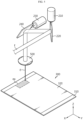
- FIG. 1 is a schematic diagram of an etching machine according to an embodiment of the present disclosure.
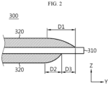
- FIG. 2 is a diagram showing an example of an electrode 300.
- FIG. 3 is a diagram showing an example of the electrode 300 in which an etching area (ea) is set.
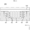
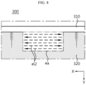
- FIG. 4 is a diagram showing the electrode 300 etched by the etching machine according to an embodiment of the present disclosure.
- the etching machine according to an embodiment of the present disclosure may include a laser source 100, a scanner 200 and a processor (not shown).
- the laser source 100 may emit light (l).
- the laser source 100 may be a laser 100 or a laser oscillator 100.
- the laser source 100 may output nanosecond (ns) pulsed light (l) having infrared wavelength. Additionally, the average output of the laser source 100 may be approximately 100W to 500W. Additionally, the laser source 100 may be a fiber laser.
- the light (l) from the laser source 100 may have the wavelength of approximately 1030 to 1070 nm. Additionally, the pulse width of the light (l) from the laser source 100 may be approximately 10 to 500 ns. Additionally, the laser beam quality M2 of the laser source 100 may be approximately smaller than 1.7. Additionally, the pulse repetition frequency of the laser source 100 may be approximately 100 to 1000 kHz.
- the scanner 200 may deflect the light (l) from the laser source 100 to an electrode current collector 310 coated with an active material or the electrode 300.
- the scanner 200 may deflect the light (l) in at least one of X axis direction or Y axis direction.
- the light (l) deflected from the scanner 200 may enter the electrode 300, and etch the electrode active material 320 of the electrode 300.
- the electrode current collector 310 may have a thin plate shape.
- the electrode current collector 310 may be made of metal.
- the electrode current collector 310 may be made of aluminum or copper.
- the electrode active material 320 may be coated, formed, attached, fixed or coupled to each of two surfaces of the electrode current collector 310.
- the electrode active material 320 and the electrode current collector 310 may constitute the electrode 300.
- the electrode active material 320 in a flowable state like a slurry may be coated on the electrode current collector 310.
- the coated electrode active material 320 may flow while it is dried. Accordingly, the electrode active material 320 may slide at the boundary between a portion of the electrode current collector 310 coated with the electrode active material 320 and a portion of the electrode current collector 310 not coated with the electrode active material. Accordingly, the thickness at the boundary portion coated with the electrode active material 320 may have a smaller thickness than the other coated portion.
- the electrode active material 320 coated on the upper surface of the electrode 300 may slide a length D1. Additionally, the electrode active material 320 coated on the lower surface of the electrode 300 may slide a length D2.
- the process of coating the electrode active material 320 on the upper surface of the electrode current collector 310 and the process of coating the electrode active material 320 on the lower surface may be performed in a sequential order. Accordingly, the process conditions when the electrode active material 320 is coated on the upper surface of the electrode current collector 310 and the process conditions when the electrode active material 320 is coated on the lower surface of the electrode current collector 310 may be different from each other.
- the temperature and humidity of the electrode active material 320 slurry, the temperature and humidity around a coater and the temperature and processing speed of the coater may change during the process. Accordingly, the location at which the electrode active material 320 coated on the upper surface of the electrode current collector 310 starts to slide and the location at which the electrode active material 320 coated on the lower surface of the electrode current collector 310 starts to slide may not match to each other. Additionally, the slide length of the electrode active material 320 coated on the upper surface of the electrode current collector 310 and the slide length of the electrode active material 320 coated on the lower surface of the electrode current collector 310 may be different from each other. Referring to FIG.
- the electrode active materials 320 coated on the two surfaces of the electrode current collector 310 may have the mismatch of a length D3. Accordingly, electrode capacity may reduce, and Li plating, i.e., deposition of lithium included in the electrode active material 320 may occur a loading difference between a positive electrode active material and a negative electrode active material opposite the positive electrode active material.
- the etching machine may be configured to etch at least one of the electrode active material 320 coated on the upper surface of the electrode current collector 310 or the electrode active material 320 coated on the lower surface of the electrode current collector 310.
- the etching machine according to an embodiment of the present disclosure may etch the electrode 300 to match the coating area of the electrode active material 320 coated on the upper surface of the electrode current collector 310 and the coating area of the electrode active material 320 coated on the lower surface of the electrode current collector 310.
- the etching machine may etch the electrode 300 to remove the slide area of the electrode active material 320 coated on the upper surface of the electrode current collector 310 or the slide area of the electrode active material 320 coated on the lower surface of the electrode current collector 310.
- the processor of an electrode device may set the etching area (ea) as much as a width D4 from the boundary between the area coated with the electrode active material 320 and the uncoated area before the etching.
- the width D4 may be a length including the slide area occurring at the coated electrode active material 320.
- the etching area (ea) may extend along X axis direction while maintaining the width D4.
- the processor may control at least one of the laser source 100 or the scanner 200.
- the processor may perform on/off control of the output of the laser source 100.
- the processor may control a laser trigger signal of the laser source 100.
- the laser trigger signal may be referred to as a laser signal or a trigger signal.
- the processor may control the scanner 200 to adjust the deflection of the light (l).
- the processor may allow the light (l) from the laser source 100 to enter the electrode current collector 310 coated with the electrode active material 320 or the electrode 300.
- the processor may control the laser source 100 and the scanner 200 to control the light (l) incident on the electrode 300 to move along a straight line.
- a movement path of the light (l) may referred to as an etching line (el).
- the etching line (el) may include a plurality of etching lines (el). Additionally, the plurality of etching lines (el) may be arranged at a regular interval in the etching area (ea).
- the processor may control at least one of the laser source 100 or the scanner 200 to keep a pulse distance D5 of the light (l) incident on the electrode current collector 310 coated with the electrode active material 320 or the electrode 300 constant.
- the pulse distance D5 of the light (l) may be constant along the etching line (el).
- the processor may control at least one of the laser source 100 or the scanner 200 to keep a pulse overlap D6 or pulse overlap rate (D6) of the light (l) incident on the electrode current collector 310 coated with the electrode active material 320 or the electrode 300 constant.
- the pulse overlap D6 or pulse overlap rate (D6) of the light (l) may be constant along the etching line (el).
- the pulse overlap rate (D6) may be approximately 50%.
- the line energy or energy density transmitted to the electrode 300 may be uniform during the etching of the electrode 300. Accordingly, it may be possible to remove only the electrode active material 320 with minimal damage to the electrode current collector 310.
- the present disclosure it may be possible to remove the slide occurred at the peripheral area of the electrode active material 320 coated on the electrode current collector 310 or the boundary area between the coated area with the electrode active material 320 and the uncoated area. Accordingly, it may be possible to improve the quality of the electrode 300.
- the electrode active material 320 coated on the two surfaces of the electrode current collector 310 may match. Accordingly, it may be possible to increase the capacity of the electrode 300 and improve the quality of the electrode 300.
- the etching machine may include a beam expander 400.
- the light (l) from the laser source 100 may enter the scanner 200 via the beam expander 400.
- the beam expander 400 may be configured to adjust the diameter or divergence angle of the light (l) from the laser source 100.
- the etching machine may optionally include the beam expander 400 to precisely control the light (l).
- the etching machine may include a condensing lens 500.
- the condensing lens 500 may converge the light (l) deflected through the scanner 200 at a single point. That is, the condensing lens 500 may converge the light (l) deflected through the scanner 200 at a single point on the surface of the electrode active material 320 coated on the electrode current collector 310.
- the condensing lens 500 may be an f-theta focusing lens.
- the effective focal length of the condensing lens 500 may be approximately 250 mm or more and 420 mm or less. Additionally, the fluence of the light (l) from the laser source 100 may be approximately 7J/cm 2 or more and 12 J/cm 2 or less.
- the volume of the electrode active material 320 that may be removed or etched per pulse increase.
- the fluence of the light (l) exceeds the melting threshold or vaporization threshold of the metal (aluminum or copper) of which the electrode current collector 310 is made, the electrode current collector 310 may be damaged or melt.
- the diameter and pulse energy of the light (l) may be calculated by controlling at least one of the diameter of the light (l) from the laser source 100, the focal length of the condensing lens 500 or the magnification of the beam expander 400.
- the processor may control the fluence of the light (l) from the laser source 100 to prevent it from exceeding the melting threshold or vaporization threshold of the electrode current collector 310.
- the beam expander 400 of the etching machine may be used in combination with the plurality of laser sources 100.
- the light (l) from the laser source 100 is usually approximately 7 to 9 mm in diameter, and when the light (l) spreads out, it results in low output and consequential low process efficiency. Accordingly, to increase the process efficiency, the plurality of laser sources 100 may be arranged in parallel, one beam expander 400 may be used, and the diameter and divergence angle of the light (l) from the plurality of laser sources 100 may be controlled at one time.
- the effective focal length of the condensing lens 500 may be approximately 250 mm or more and 420 mm or less. Accordingly, the effective process window may be largest. Additionally, it may be possible to reduce the influence of a change in focal length caused by a small change in output of the laser source 100 or vibration or a change in diameter of the light (l) from the laser source 100.
- the etching machine may include a stage 600.
- the stage 600 may be referred to as a die 600.
- the electrode 300 may be placed on the stage 600.
- the stage 600 may support or hold the electrode 300.
- the stage 600 may be movable, and the processor may control the movement of the stage 600. Accordingly, the electrode 300 placed on the stage 600 may be movable.
- the laser source 100 of the etching machine may output nanosecond (ns) light (l) having infrared wavelength. Accordingly, the etching machine may remove only the electrode active material 320 with minimal damage to the electrode current collector 310. In contrast, when light (l) with picosecond (ps) or shorter pulse width is used to etch the electrode 300, there may be a higher damage risk of the electrode current collector 310. Additionally, when light in wavelengths corresponding to green light or wavelengths corresponding to ultraviolet light is used to etch the electrode 300, there may be a higher damage risk of the electrode current collector 310.
- the processor of the etching machine may perform control to scan multiple times in the etching area (ea).
- the processor may perform control to scan multiple times along the etching line (el).
- the number of scans may be 2.
- the coating thickness of the electrode active material 320 is approximately 150 ⁇ m or more, the number of scans may be 3.
- the laser fluence that is higher than the melting threshold of the electrode current collector 310 is used, and this may increase the damage risk of the electrode current collector 310. Additionally, when scanning is conducted four or more times, damage to the electrode current collector 310 may be prevented, but the processing time may be longer. Accordingly, scanning may be preferably conducted two or three times.
- FIG. 5 is a schematic diagram of part of the process of etching the electrode 300 by the etching machine according to an embodiment of the present disclosure.
- FIG. 6 is a diagram showing an example of etching the electrode 300 by the etching machine according to an embodiment of the present disclosure.
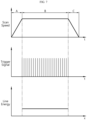
- FIG. 7 is a graph showing changes in control variables of the etching machine according to an embodiment of the present disclosure during the etching of the electrode 300 by the etching machine.
- the processor of the etching machine may stop the output of the laser source 100 while the scan speed of the scanner 200 increases or decreases.
- the etching area (ea) may include the plurality of etching lines (el1).
- directions in which the adjacent etching lines (el1) run may be opposite. Accordingly, to proceed with the etching from any one etching line (el1) to the next etching line (el1), it may be necessary to change the scan direction. Additionally, before the scan direction changes, the scan speed may decrease and become zero (0). Additionally, after the scan speed becomes zero (0), the scan direction may change and the scan speed may increase. In contrast, the scan speed may be kept constant during the etching along the etching line (el1). In this instance, the etching line (el1) may be referred to as a scan line (el1).
- the processor may turn off the output of the laser source while the scan direction changes or while the scan speed decreases and becomes zero (0) and then increases. That is, the processor may only turn on the output of the laser source 100 while the scan speed is kept constant.
- an imaginary trajectory (dcl) of scan focus points of the scanner 200 may connect the adjacent etching lines (el1).
- the imaginary trajectory (dcl) of scan focus points may connect the ending point of any one etching line (el1) to the starting point of the adjacent etching line (el1).
- the imaginary trajectory (dcl) of scan focus points may be referred to as an imaginary scan line (dcl), a scan line (dcl) or a direction change line (dcl).
- the imaginary trajectory (dcl) of scan focus points may be located outside of the etching area (ea).
- the processor may off the trigger signal to the laser source 100 while the scan speed increases (range A). Accordingly, the line energy transmitted to the electrode 300 while the scan speed increases (range A) may be zero (0).
- the processor may transmit the trigger signal to the laser source 100 at a regular interval while the scan speed is kept constant (range B). Accordingly, the line energy transmitted to the electrode 300 while the scan speed is kept constant (range B) may maintain a constant value. In this instance, the processor may etch the electrode 300 while maintaining a constant pulse distance along the etching line (el1).
- the processor may off the trigger signal to the laser source 100 while the scan speed decreases (range C). Accordingly, the line energy transmitted to the electrode 300 while the scan speed decreases (range C) may be zero (0).
- the electrode 300 may be etched at a uniform level in the etching area (ea). Accordingly, it may be easy to perform control to etch the electrode active material 320 without damage to the electrode current collector 310.
- the scanner of the etching machine may include mirrors 220, 240 to reflect the light (l) from the laser source 100, and motors 210, 230 to rotate the mirrors 220, 240. Additionally, the processor may control the laser source 100 to stop the output of the laser source 100 while the angular velocity of the motors 210, 230 increases or decreases.
- the scanner 200 may include at least one mirror 220, 240.
- the scanner 200 may include a first mirror 220 and a second mirror 240.
- the first mirror 220 may deflect the light (l) in Y axis direction.
- the second mirror 240 may deflect the light (l) in X axis direction.
- the first mirror 220 may be connected to a rotation axis of a first motor 210.
- the second mirror 240 may be connected to a rotation axis of a second motor 230.
- the first motor 210 may rotate the first mirror 220.
- the second motor 230 may rotate the second mirror 240.
- the processor may deflect the light (l) from the laser source 100 with respect to the X-Y plane by controlling the rotation of the first motor 210 and the second motor 230. Specifically, the processor may control the scan speed of the etching machine by controlling the angular velocity of the first motor 210 and the angular velocity of the second motor 230.
- the scanner 200 may further include an encoder at the motors 210, 230 or the mirrors 220, 240. The processor may detect the angular velocity of the motors 210, 230 or the mirrors 220, 240 from the encoder.
- the processor may control the laser source 100 so as not to output the laser source 100 while the angular velocity of at least one of the first motor 210 or the second motor 230 increases or decreases.
- the imaginary trajectory (dcl) of scan focus points of the scanner 200 may connect the adjacent etching lines (el1).
- the imaginary trajectory (dcl) of scan focus points may connect the ending point of any one etching line (el1) to the starting point of the adjacent etching line (el1).
- the line energy transmitted to the electrode 300 while the angular velocity of at least one of the first motor 210 or the second motor 230 increases or decreases may be zero (0).
- the processor may transmit the trigger signal to the laser source 100 at a regular interval while the angular velocity of at least one of the first motor 210 or the second motor 230 is kept constant (range B). Accordingly, the line energy transmitted to the electrode 300 while the angular velocity of at least one of the first motor 210 or the second motor 230 is kept constant (range B) may maintain a constant value. In this instance, the processor may etch the electrode 300 while maintaining a constant pulse distance along the etching line (el1).
- the electrode 300 may be etched at a uniform level in the etching area (ea). Accordingly, it may be easy to perform control to etch the electrode active material 320 without damage to the electrode current collector 310.
- FIG. 8 is a diagram showing an example of etching the electrode 300 by the etching machine according to an embodiment of the present disclosure.
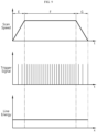
- FIG. 9 is a graph showing changes in control variables of the etching machine according to an embodiment of the present disclosure during the etching of the electrode 300 by the etching machine.
- the processor of the etching machine may perform control to reduce a trigger signal interval of the laser source 100 with the increasing scan speed of the scanner 200.
- the processor may perform control to reduce the trigger signal interval of the laser source 100 with the increasing scan speed of the scanner 200 (range E), to keep the pulse distance of the light (l) incident on the electrode 300 constant.
- the processor may perform control to keep the trigger signal interval of the laser source 100 constant while the scan speed of the scanner 200 is kept constant (range F), to keep the pulse distance of the light (l) incident on the electrode 300 constant.
- the processor may control the laser source 100 to make the pulse distance at the increasing scan speed of the scanner 200 and the pulse distance at the constant scan speed equal to each other. Additionally, the processor may control the laser source 100 to make the line energy transmitted to the electrode 300 at the increasing scan speed of the scanner 200 and the line energy transmitted to the electrode 300 at the constant scan speed equal to each other.
- the pulse distance at the electrode 300 may be constant, and the electrode 300 may be etched at a uniform level in the etching area (ea). Accordingly, it may be easy to perform control to etch the electrode active material 320 without damage to the electrode current collector 310.
- the processor of the etching machine may perform control to increase the trigger signal interval of the laser source 100 with the decreasing scan speed of the scanner 200.
- the processor may perform control to increase the trigger signal interval of the laser source 100 with the decreasing scan speed of the scanner 200 (range G), to keep the pulse distance of the light (l) incident on the electrode 300 constant.
- the processor may perform control to keep the trigger signal interval of the laser source 100 constant while the scan speed of the scanner 200 is kept constant (range F), to keep the pulse distance of the light (l) incident on the electrode 300 constant.
- the processor may control the laser source 100 to make the pulse distance at the decreasing scan speed of the scanner 200 and the pulse distance at the constant scan speed equal to each other. Additionally, the processor may control the laser source 100 to make the line energy transmitted to the electrode 300 at the decreasing scan speed of the scanner 200 and the line energy transmitted to the electrode 300 at the constant scan speed equal to each other.
- the pulse distance at the electrode 300 may be constant, and the electrode 300 may be etched at a uniform level in the etching area (ea). Accordingly, it may be easy to perform control to etch the electrode active material 320 without damage to the electrode current collector 310.
- the processor of the etching machine may reduce the trigger signal interval of the laser source 100 with the increasing angular velocity of the motors 210, 230.
- the processor may perform control to reduce the trigger signal interval of the laser source 100 with the increasing angular velocity of at least one of the first motor 210 or the second motor 230 of the scanner 200 (range E), to keep the pulse distance of the light (l) incident on the electrode 300 constant.
- the processor may perform control to keep the trigger signal interval of the laser source 100 constant while the angular velocity of at least one of the first motor 210 or the second motor 230 of the scanner 200 is kept constant (range F), to keep the pulse distance of the light (l) incident on the electrode 300 constant.
- the processor may control the laser source 100 to make the pulse distance at the increasing angular velocity of at least one of the first motor 210 or the second motor 230 of the scanner 200 and the pulse distance at the constant angular velocity of at least one of the first motor 210 or the second motor 230 equal to each other. Additionally, the processor may control the laser source 100 to make the line energy transmitted to the electrode 300 at the increasing angular velocity of at least one of the first motor 210 or the second motor 230 of the scanner 200 and the line energy transmitted to the electrode 300 at the constant angular velocity of at least one of the first motor 210 or the second motor 230 equal to each other.
- the pulse distance at the electrode 300 may be constant, and the electrode 300 may be etched at a uniform level in the etching area (ea). Accordingly, it may be easy to perform control to etch the electrode active material 320 without damage to the electrode current collector 310.
- the processor of the etching machine may perform control to increase the trigger signal interval of the laser source 100 with the decreasing angular velocity of the motors 210, 230.
- the processor may increase the trigger signal interval of the laser source 100 with the decreasing angular velocity of at least one of the first motor 210 or the second motor 230 of the scanner 200 (range G), to keep the pulse distance of the light (l) incident on the electrode 300 constant.
- the processor may keep the trigger signal interval of the laser source 100 constant while the angular velocity of at least one of the first motor 210 or the second motor 230 of the scanner 200 is kept constant (range F), to keep the pulse distance of the light (l) incident on the electrode 300 constant.
- the processor may control the laser source 100 to make the pulse distance at the decreasing angular velocity of at least one of the first motor 210 or the second motor 230 of the scanner 200 and the pulse distance at the constant angular velocity of at least one of the first motor 210 or the second motor 230 equal to each other. Additionally, the processor may control the laser source 100 to make the line energy transmitted to the electrode 300 at the decreasing angular velocity of at least one of the first motor 210 or the second motor 230 of the scanner 200 and the line energy transmitted to the electrode 300 at the constant angular velocity of at least one of the first motor 210 or the second motor 230 equal to each other.
- the pulse distance at the electrode 300 may be constant, and the electrode 300 may be etched at a uniform level in the etching area (ea). Accordingly, it may be easy to perform control to etch the electrode active material 320 without damage to the electrode current collector 310.
- the processor of the etching machine may perform control to keep the trigger signal interval of the laser source 100 constant while the scan speed of the scanner 200 is kept constant.
- the processor of the etching machine may control at least one of the laser source 100 or the scanner 200 to keep the line energy density along the trajectory of the light (l) incident on the electrode current collector 310 constant.
- the electrode 300 may be etched at a uniform level in the etching area (ea). Accordingly, it may be easy to perform control to etch the electrode active material 320 without damage to the electrode current collector 310.
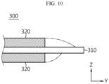
- FIG. 10 is a side view of the electrode 300 etched by the etching machine according to an embodiment of the present disclosure.
- the electrode 300 etched by the etching machine according to an embodiment of the present disclosure may have the electrode active material 320 coating areas on the two surfaces matched to each other. Additionally, the electrode active material 320 coating on the two surfaces of the electrode 300 may be configured to remove the slide area. Accordingly, the thickness of the electrode active material 320 coating area may be constant.
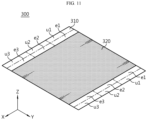
- FIG. 11 is a perspective view of the electrode 300 etched by the etching machine according to an embodiment of the present disclosure.
- FIG. 12 is a perspective view of a tab 330 formed at the electrode 300 etched by the etching machine according to an embodiment of the present disclosure.
- the electrode 300 etched by the etching machine according to an embodiment of the present disclosure may include the tab 330.
- the electrode 300 may include areas u1, u2, u3 where the electrode 300 is not coated with the electrode active material 320 and areas e1, e2, e3 where the electrode 300 is coated with the electrode active material 320 and etched.
- the remaining areas u2, e2 may be the tab 330.
- the tab 330 may be a portion of the electrode current collector 310. At least a portion of the tab 330 may be the area u2 not coated with the electrode active material 320, and the remainder may be the area e2 coated with the electrode active material 320 and etched.
- the tab 330 may have uniform thickness and color. Meanwhile, the areas e1, e2 on two sides of the etched area e2 among the areas u2, e2 that may be used as the tab 330 will be cut and removed, so they may not be etched to increase the process efficiency.
- a battery cell may include the electrode 300 etched by the etching machine of the present disclosure.
- the electrode 300 of the present disclosure may be a positive electrode and/or a negative electrode.
- the positive electrode and the negative electrode may be stacked with a separator interposed between them to form an electrode assembly.
- the positive electrode and/or negative electrode may include a plurality of positive electrodes and/or negative electrodes, and the plurality of tabs 330 of the plurality of electrodes having the same polarity may be electrically connected to electrode leads.
- the plurality of electrodes 300 may constitute the battery cell.
- the battery cell may be a pouch-type secondary battery.
- the pouch-type secondary battery may include a pouch packaging accommodating the electrode 300 and an electrolyte.
- the pouch packaging may be formed by sealing the edge of two pouches in which the electrode 300 and the electrolyte are received.
- the pouch-type secondary battery may include an accommodation portion at the center and a sealing portion around the accommodation portion.
- the pouch-type secondary battery may have a rectangular shape with four edges, and among the four edges, three or four edges may be sealed.
- a battery module according to an aspect of the present disclosure may include the electrode 300 etched by the etching machine of the present disclosure.
- the battery module may further include a variety of other components, for example, components of the battery module known at the time the application was filed, such as a busbar assembly, a module case, a cooling unit and so on.
- a battery pack according to an aspect of the present disclosure may include the electrode 300 etched by the etching machine of the present disclosure.
- the battery pack may further include a variety of other components, for example, components of the battery pack known at the time the application was filed, such as a battery management system (BMS), a busbar, a pack case, a relay, a current sensor and so on.
- BMS battery management system
Landscapes
- Physics & Mathematics (AREA)
- Optics & Photonics (AREA)
- Engineering & Computer Science (AREA)
- Plasma & Fusion (AREA)
- Mechanical Engineering (AREA)
- Chemical & Material Sciences (AREA)
- Chemical Kinetics & Catalysis (AREA)
- Electrochemistry (AREA)
- General Chemical & Material Sciences (AREA)
- Manufacturing & Machinery (AREA)
- Materials Engineering (AREA)
- Laser Beam Processing (AREA)
- Manufacturing Of Printed Circuit Boards (AREA)
- Battery Electrode And Active Subsutance (AREA)
Abstract
Description
- The present disclosure relates to an etching machine.
- The present application claims priority to
Korean Patent Application No. 10-2022-0182357 filed on December 22, 2022 Korean Patent Application No. 10-2023-0027291 filed on February 28, 2023 - With a rapid increase in demand for portable electronic products such as laptop computers, video cameras, mobile phones and so on and the widespread use of robots, electric vehicles and so on, many studies are being made on high performance secondary batteries that can be recharged repeatedly.
- Currently, commercially available secondary batteries include nickel-cadmium batteries, nickel-hydrogen batteries, nickel-zinc batteries, lithium secondary batteries and so on, and among them, lithium secondary batteries have little or no memory effect, and thus they are gaining more attention than nickel-based secondary batteries for their advantages that recharging can be done whenever it is convenient, the self-discharge rate is very low and the energy density is high.
- Lithium secondary batteries primarily comprise lithium-based oxides and carbon materials for a positive electrode active material and a negative electrode active material, respectively. A lithium secondary battery includes an electrode assembly including a positive electrode plate and a negative electrode plate coated with the positive electrode active material and the negative electrode active material, respectively, with a separator interposed between the positive electrode plate and the negative electrode plate, and a sealed packaging or battery case accommodating the electrode assembly together with an electrolyte solution.
- When manufacturing the electrode, a process of coating the positive electrode active material or the negative electrode active material on an electrode current collector may be performed. In this instance, when the coating areas on two surfaces of the electrode current collector are different, it results in low quality of the battery cell. Additionally, a slide phenomenon that occurs when the electrode active material in slurry state coated on the electrode current collector flows during drying, may degrade the quality of the battery cell.
- The present disclosure is designed to solve these and other problems.
- The present disclosure is directed to providing an electrode with improved active material coating quality of an electrode current collector.
- The present disclosure is further directed to providing an electrode having the equal active material coating area on two surfaces of the electrode current collector.
- The present disclosure is further directed to providing an etching machine for etching a peripheral portion of the coating using a laser to make the active material coating area on the two surfaces of the electrode current collector equal.
- The present disclosure is further directed to providing an etching machine for minimizing damage to the electrode current collector when laser etching the peripheral portion of the active material coating on the electrode current collector.
- To solve the above-described problem, an etching machine according to an embodiment of the present disclosure includes a laser source; a scanner configured to deflect light from the laser source to an electrode current collector coated with an electrode active material; and a processor configured to control at least one of the laser source or the scanner to keep a pulse distance of the light incident on the electrode current collector constant.
- Additionally, the processor may stop the output of the laser source while a scan speed of the scanner increases or decreases.
- Additionally, the scanner may include a mirror configured to reflect the light from the laser source; and a motor configured to rotate the mirror, and the processor may stop the output of the laser source while an angular velocity of the motor increases or decreases.
- Additionally, the processor may perform control to reduce a trigger signal interval of the laser source with an increasing scan speed of the scanner.
- Additionally, the scanner include a mirror configured to reflect the light from the laser source; and a motor configured to rotate the mirror, and the processor may perform control to reduce a trigger signal interval of the laser source with an increasing angular velocity of the motor.
- Additionally, the processor may perform control to increase a trigger signal interval of the laser source with a decreasing scan speed of the scanner.
- Additionally, the scanner may include a mirror configured to reflect the light from the laser source; and a motor configured to rotate the mirror, and the processor may perform control to increase a trigger signal interval of the laser source with a decreasing angular velocity of the motor.
- Additionally, the processor may perform control to keep a trigger signal interval of the laser source constant while a scan speed of the scanner is kept constant.
- Additionally, the processor may control at least one of the laser source or the scanner to keep a line energy density constant along a trajectory of the light incident on the electrode current collector.
- An electrode according to an aspect of the present disclosure is an electrode etched by the etching machine according to the present disclosure.
- A battery cell according to an aspect of the present disclosure includes the electrode etched by the etching machine according to the present disclosure.
- A battery module according to an aspect of the present disclosure includes the electrode etched by the etching machine according to the present disclosure.
- A battery pack according to an aspect of the present disclosure includes the electrode etched by the etching machine according to the present disclosure.
- According to at least one of the embodiments of the present disclosure, it may be possible to provide the electrode with improved active material coating quality of the electrode current collector.
- According to at least one of the embodiments of the present disclosure, it may be possible to provide the electrode having the equal active material coating area on the two surfaces of the electrode current collector.
- According to at least one of the embodiments of the present disclosure, it may be possible to provide the etching machine for etching the peripheral portion of the coating using a laser to make the active material coating area on the two surfaces of the electrode current collector equal.
- According to at least one of the embodiments of the present disclosure, it may be possible to provide the etching machine for minimizing damage to the electrode current collector when laser etching the peripheral portion of the active material coating on the electrode current collector.
- The present disclosure may have many other effects, and these effects will be described in each embodiment, or regarding effects that can be easily anticipated by those skilled in the art, the corresponding description is omitted.
- The accompanying drawings illustrate exemplary embodiments of the present disclosure and together with the following detailed description, serve to provide a further understanding of the technical aspect of the present disclosure, and thus the present disclosure should not be construed as being limited to the drawings.
-
FIG. 1 is a schematic diagram of an etching machine according to an embodiment of the present disclosure. -
FIG. 2 is a diagram showing an example of an electrode. -
FIG. 3 is a diagram showing an example of an electrode in which an etching area is set. -
FIG. 4 is a diagram showing an electrode etched by an etching machine according to an embodiment of the present disclosure. -
FIG. 5 is a schematic diagram of part of a process of etching an electrode by an etching machine according to an embodiment of the present disclosure. -
FIG. 6 is a diagram showing an example of etching an electrode by an etching machine according to an embodiment of the present disclosure. -
FIG. 7 is a graph showing changes in control variables of an etching machine according to an embodiment of the present disclosure during etching of an electrode by the etching machine. -
FIG. 8 is a diagram showing an example of etching an electrode by an etching machine according to an embodiment of the present disclosure. -
FIG. 9 is a graph showing changes in control variables of an etching machine according to an embodiment of the present disclosure during etching of an electrode by the etching machine. -
FIG. 10 is a side view of an electrode etched by an etching machine according to an embodiment of the present disclosure. -
FIG. 11 is a perspective view of an electrode etched by an etching machine according to an embodiment of the present disclosure. -
FIG. 12 is a perspective view of a tab formed at an electrode etched by an etching machine according to an embodiment of the present disclosure. - Hereinafter, exemplary embodiments of the present disclosure will be described in detail with reference to the accompanying drawings. Prior to the description, it should be understood that the terms or words used in the specification and the appended claims should not be construed as being limited to general and dictionary meanings, but rather interpreted based on the meanings and concepts corresponding to the technical aspect of the present disclosure on the basis of the principle that the inventor is allowed to define the terms appropriately for the best explanation.
- Therefore, the embodiments described herein and the illustrations shown in the drawings are exemplary embodiments of the present disclosure to describe the technical aspect of the present disclosure and are not intended to be limiting, so it should be understood that a variety of other equivalents and modifications could have been made thereto at the time that the application was filed.
-
FIG. 1 is a schematic diagram of an etching machine according to an embodiment of the present disclosure.FIG. 2 is a diagram showing an example of anelectrode 300.FIG. 3 is a diagram showing an example of theelectrode 300 in which an etching area (ea) is set.FIG. 4 is a diagram showing theelectrode 300 etched by the etching machine according to an embodiment of the present disclosure. Referring toFIGS. 1 to 4 , the etching machine according to an embodiment of the present disclosure may include alaser source 100, ascanner 200 and a processor (not shown). - The
laser source 100 may emit light (l). Thelaser source 100 may be alaser 100 or alaser oscillator 100. Thelaser source 100 may output nanosecond (ns) pulsed light (l) having infrared wavelength. Additionally, the average output of thelaser source 100 may be approximately 100W to 500W. Additionally, thelaser source 100 may be a fiber laser. - The light (l) from the
laser source 100 may have the wavelength of approximately 1030 to 1070 nm. Additionally, the pulse width of the light (l) from thelaser source 100 may be approximately 10 to 500 ns. Additionally, the laser beam quality M2 of thelaser source 100 may be approximately smaller than 1.7. Additionally, the pulse repetition frequency of thelaser source 100 may be approximately 100 to 1000 kHz. - The
scanner 200 may deflect the light (l) from thelaser source 100 to an electrodecurrent collector 310 coated with an active material or theelectrode 300. Thescanner 200 may deflect the light (l) in at least one of X axis direction or Y axis direction. The light (l) deflected from thescanner 200 may enter theelectrode 300, and etch the electrodeactive material 320 of theelectrode 300. - The electrode
current collector 310 may have a thin plate shape. The electrodecurrent collector 310 may be made of metal. For example, the electrodecurrent collector 310 may be made of aluminum or copper. The electrodeactive material 320 may be coated, formed, attached, fixed or coupled to each of two surfaces of the electrodecurrent collector 310. The electrodeactive material 320 and the electrodecurrent collector 310 may constitute theelectrode 300. In this instance, the electrodeactive material 320 in a flowable state like a slurry may be coated on the electrodecurrent collector 310. The coated electrodeactive material 320 may flow while it is dried. Accordingly, the electrodeactive material 320 may slide at the boundary between a portion of the electrodecurrent collector 310 coated with the electrodeactive material 320 and a portion of the electrodecurrent collector 310 not coated with the electrode active material. Accordingly, the thickness at the boundary portion coated with the electrodeactive material 320 may have a smaller thickness than the other coated portion. - Referring to
FIG. 2 , the electrodeactive material 320 coated on the upper surface of theelectrode 300 may slide a length D1. Additionally, the electrodeactive material 320 coated on the lower surface of theelectrode 300 may slide a length D2. The process of coating the electrodeactive material 320 on the upper surface of the electrodecurrent collector 310 and the process of coating the electrodeactive material 320 on the lower surface may be performed in a sequential order. Accordingly, the process conditions when the electrodeactive material 320 is coated on the upper surface of the electrodecurrent collector 310 and the process conditions when the electrodeactive material 320 is coated on the lower surface of the electrodecurrent collector 310 may be different from each other. For example, the temperature and humidity of the electrodeactive material 320 slurry, the temperature and humidity around a coater and the temperature and processing speed of the coater may change during the process. Accordingly, the location at which the electrodeactive material 320 coated on the upper surface of the electrodecurrent collector 310 starts to slide and the location at which the electrodeactive material 320 coated on the lower surface of the electrodecurrent collector 310 starts to slide may not match to each other. Additionally, the slide length of the electrodeactive material 320 coated on the upper surface of the electrodecurrent collector 310 and the slide length of the electrodeactive material 320 coated on the lower surface of the electrodecurrent collector 310 may be different from each other. Referring toFIG. 2 , the electrodeactive materials 320 coated on the two surfaces of the electrodecurrent collector 310 may have the mismatch of a length D3. Accordingly, electrode capacity may reduce, and Li plating, i.e., deposition of lithium included in the electrodeactive material 320 may occur a loading difference between a positive electrode active material and a negative electrode active material opposite the positive electrode active material. - Referring to
FIG. 3 , the etching machine according to an embodiment of the present disclosure may be configured to etch at least one of the electrodeactive material 320 coated on the upper surface of the electrodecurrent collector 310 or the electrodeactive material 320 coated on the lower surface of the electrodecurrent collector 310. The etching machine according to an embodiment of the present disclosure may etch theelectrode 300 to match the coating area of the electrodeactive material 320 coated on the upper surface of the electrodecurrent collector 310 and the coating area of the electrodeactive material 320 coated on the lower surface of the electrodecurrent collector 310. Additionally, the etching machine according to an embodiment of the present disclosure may etch theelectrode 300 to remove the slide area of the electrodeactive material 320 coated on the upper surface of the electrodecurrent collector 310 or the slide area of the electrodeactive material 320 coated on the lower surface of the electrodecurrent collector 310. For example, referring toFIG. 3 , the processor of an electrode device may set the etching area (ea) as much as a width D4 from the boundary between the area coated with the electrodeactive material 320 and the uncoated area before the etching. The width D4 may be a length including the slide area occurring at the coated electrodeactive material 320. The etching area (ea) may extend along X axis direction while maintaining the width D4. - Referring to
FIG. 4 , the processor may control at least one of thelaser source 100 or thescanner 200. The processor may perform on/off control of the output of thelaser source 100. Additionally, the processor may control a laser trigger signal of thelaser source 100. The laser trigger signal may be referred to as a laser signal or a trigger signal. Additionally, the processor may control thescanner 200 to adjust the deflection of the light (l). The processor may allow the light (l) from thelaser source 100 to enter the electrodecurrent collector 310 coated with the electrodeactive material 320 or theelectrode 300. The processor may control thelaser source 100 and thescanner 200 to control the light (l) incident on theelectrode 300 to move along a straight line. In this instance, a movement path of the light (l) may referred to as an etching line (el). The etching line (el) may include a plurality of etching lines (el). Additionally, the plurality of etching lines (el) may be arranged at a regular interval in the etching area (ea). The processor may control at least one of thelaser source 100 or thescanner 200 to keep a pulse distance D5 of the light (l) incident on the electrodecurrent collector 310 coated with the electrodeactive material 320 or theelectrode 300 constant. The pulse distance D5 of the light (l) may be constant along the etching line (el). Additionally, the processor may control at least one of thelaser source 100 or thescanner 200 to keep a pulse overlap D6 or pulse overlap rate (D6) of the light (l) incident on the electrodecurrent collector 310 coated with the electrodeactive material 320 or theelectrode 300 constant. The pulse overlap D6 or pulse overlap rate (D6) of the light (l) may be constant along the etching line (el). For example, the pulse overlap rate (D6) may be approximately 50%. - According to the above-described configuration of the present disclosure, the line energy or energy density transmitted to the
electrode 300 may be uniform during the etching of theelectrode 300. Accordingly, it may be possible to remove only the electrodeactive material 320 with minimal damage to the electrodecurrent collector 310. - Additionally, according to the above-described configuration of the present disclosure, it may be possible to remove the slide occurred at the peripheral area of the electrode
active material 320 coated on the electrodecurrent collector 310 or the boundary area between the coated area with the electrodeactive material 320 and the uncoated area. Accordingly, it may be possible to improve the quality of theelectrode 300. - Additionally, according to the above-described configuration of the present disclosure, the electrode
active material 320 coated on the two surfaces of the electrodecurrent collector 310 may match. Accordingly, it may be possible to increase the capacity of theelectrode 300 and improve the quality of theelectrode 300. - The etching machine according to an embodiment of the present disclosure may include a
beam expander 400. The light (l) from thelaser source 100 may enter thescanner 200 via thebeam expander 400. Thebeam expander 400 may be configured to adjust the diameter or divergence angle of the light (l) from thelaser source 100. The etching machine may optionally include thebeam expander 400 to precisely control the light (l). - The etching machine according to an embodiment of the present disclosure may include a condensing
lens 500. The condensinglens 500 may converge the light (l) deflected through thescanner 200 at a single point. That is, the condensinglens 500 may converge the light (l) deflected through thescanner 200 at a single point on the surface of the electrodeactive material 320 coated on the electrodecurrent collector 310. For example, the condensinglens 500 may be an f-theta focusing lens. - In this instance, the effective focal length of the condensing
lens 500 may be approximately 250 mm or more and 420 mm or less. Additionally, the fluence of the light (l) from thelaser source 100 may be approximately 7J/cm2 or more and 12 J/cm2 or less. - As the fluence of the light (l) from the
laser source 100 is higher, the volume of the electrodeactive material 320 that may be removed or etched per pulse increase. However, when the fluence of the light (l) exceeds the melting threshold or vaporization threshold of the metal (aluminum or copper) of which the electrodecurrent collector 310 is made, the electrodecurrent collector 310 may be damaged or melt. - In this instance, the diameter and pulse energy of the light (l) may be calculated by controlling at least one of the diameter of the light (l) from the
laser source 100, the focal length of the condensinglens 500 or the magnification of thebeam expander 400. Using this, the processor may control the fluence of the light (l) from thelaser source 100 to prevent it from exceeding the melting threshold or vaporization threshold of the electrodecurrent collector 310. - The
beam expander 400 of the etching machine according to an embodiment of the present disclosure may be used in combination with the plurality oflaser sources 100. The light (l) from thelaser source 100 is usually approximately 7 to 9 mm in diameter, and when the light (l) spreads out, it results in low output and consequential low process efficiency. Accordingly, to increase the process efficiency, the plurality oflaser sources 100 may be arranged in parallel, onebeam expander 400 may be used, and the diameter and divergence angle of the light (l) from the plurality oflaser sources 100 may be controlled at one time. - In this instance, the effective focal length of the condensing
lens 500 may be approximately 250 mm or more and 420 mm or less. Accordingly, the effective process window may be largest. Additionally, it may be possible to reduce the influence of a change in focal length caused by a small change in output of thelaser source 100 or vibration or a change in diameter of the light (l) from thelaser source 100. - The etching machine according to an embodiment of the present disclosure may include a
stage 600. Thestage 600 may be referred to as adie 600. Theelectrode 300 may be placed on thestage 600. Thestage 600 may support or hold theelectrode 300. Additionally, thestage 600 may be movable, and the processor may control the movement of thestage 600. Accordingly, theelectrode 300 placed on thestage 600 may be movable. - The
laser source 100 of the etching machine according to an embodiment of the present disclosure may output nanosecond (ns) light (l) having infrared wavelength. Accordingly, the etching machine may remove only the electrodeactive material 320 with minimal damage to the electrodecurrent collector 310. In contrast, when light (l) with picosecond (ps) or shorter pulse width is used to etch theelectrode 300, there may be a higher damage risk of the electrodecurrent collector 310. Additionally, when light in wavelengths corresponding to green light or wavelengths corresponding to ultraviolet light is used to etch theelectrode 300, there may be a higher damage risk of the electrodecurrent collector 310. It is because light corresponding to green light or ultraviolet light can be absorbed by aluminum or copper of which the electrodecurrent collector 310 is made at a high absorption rate. Accordingly, it is preferred to etch using nanosecond pulsed light (l) having a low absorption rate in aluminum or copper of which the electrodecurrent collector 310 is made and a high absorption rate in the electrodeactive material 320. Accordingly, it may be possible to remove the electrodeactive material 320 without damage to the electrodecurrent collector 310. - The processor of the etching machine according to an embodiment of the present disclosure may perform control to scan multiple times in the etching area (ea). The processor may perform control to scan multiple times along the etching line (el). For example, the number of scans may be 2. In contrast, when the coating thickness of the electrode
active material 320 is approximately 150 µm or more, the number of scans may be 3. - To complete the etching of the electrode
active material 320 by single scan, the laser fluence that is higher than the melting threshold of the electrodecurrent collector 310 is used, and this may increase the damage risk of the electrodecurrent collector 310. Additionally, when scanning is conducted four or more times, damage to the electrodecurrent collector 310 may be prevented, but the processing time may be longer. Accordingly, scanning may be preferably conducted two or three times. -
FIG. 5 is a schematic diagram of part of the process of etching theelectrode 300 by the etching machine according to an embodiment of the present disclosure.FIG. 6 is a diagram showing an example of etching theelectrode 300 by the etching machine according to an embodiment of the present disclosure.FIG. 7 is a graph showing changes in control variables of the etching machine according to an embodiment of the present disclosure during the etching of theelectrode 300 by the etching machine. Referring toFIGS. 5 to 7 , the processor of the etching machine according to an embodiment of the present disclosure may stop the output of thelaser source 100 while the scan speed of thescanner 200 increases or decreases. - The etching area (ea) may include the plurality of etching lines (el1). In this instance, directions in which the adjacent etching lines (el1) run may be opposite. Accordingly, to proceed with the etching from any one etching line (el1) to the next etching line (el1), it may be necessary to change the scan direction. Additionally, before the scan direction changes, the scan speed may decrease and become zero (0). Additionally, after the scan speed becomes zero (0), the scan direction may change and the scan speed may increase. In contrast, the scan speed may be kept constant during the etching along the etching line (el1). In this instance, the etching line (el1) may be referred to as a scan line (el1).
- The processor may turn off the output of the laser source while the scan direction changes or while the scan speed decreases and becomes zero (0) and then increases. That is, the processor may only turn on the output of the
laser source 100 while the scan speed is kept constant. - While the output of the
laser source 100 is off, an imaginary trajectory (dcl) of scan focus points of thescanner 200 may connect the adjacent etching lines (el1). The imaginary trajectory (dcl) of scan focus points may connect the ending point of any one etching line (el1) to the starting point of the adjacent etching line (el1). The imaginary trajectory (dcl) of scan focus points may be referred to as an imaginary scan line (dcl), a scan line (dcl) or a direction change line (dcl). In this instance, the imaginary trajectory (dcl) of scan focus points may be located outside of the etching area (ea). - Referring to
FIG. 7 , the processor may off the trigger signal to thelaser source 100 while the scan speed increases (range A). Accordingly, the line energy transmitted to theelectrode 300 while the scan speed increases (range A) may be zero (0). - Additionally, the processor may transmit the trigger signal to the
laser source 100 at a regular interval while the scan speed is kept constant (range B). Accordingly, the line energy transmitted to theelectrode 300 while the scan speed is kept constant (range B) may maintain a constant value. In this instance, the processor may etch theelectrode 300 while maintaining a constant pulse distance along the etching line (el1). - Additionally, the processor may off the trigger signal to the
laser source 100 while the scan speed decreases (range C). Accordingly, the line energy transmitted to theelectrode 300 while the scan speed decreases (range C) may be zero (0). - According to the above-described configuration of the present disclosure, the
electrode 300 may be etched at a uniform level in the etching area (ea). Accordingly, it may be easy to perform control to etch the electrodeactive material 320 without damage to the electrodecurrent collector 310. - Referring to
FIGS. 5 to 7 , the scanner of the etching machine according to an embodiment of the present disclosure may includemirrors laser source 100, andmotors mirrors laser source 100 to stop the output of thelaser source 100 while the angular velocity of themotors - The
scanner 200 may include at least onemirror scanner 200 may include afirst mirror 220 and asecond mirror 240. For example, thefirst mirror 220 may deflect the light (l) in Y axis direction. Additionally, thesecond mirror 240 may deflect the light (l) in X axis direction. Thefirst mirror 220 may be connected to a rotation axis of afirst motor 210. Additionally, thesecond mirror 240 may be connected to a rotation axis of asecond motor 230. Thefirst motor 210 may rotate thefirst mirror 220. Thesecond motor 230 may rotate thesecond mirror 240. The processor may deflect the light (l) from thelaser source 100 with respect to the X-Y plane by controlling the rotation of thefirst motor 210 and thesecond motor 230. Specifically, the processor may control the scan speed of the etching machine by controlling the angular velocity of thefirst motor 210 and the angular velocity of thesecond motor 230. In this instance, thescanner 200 may further include an encoder at themotors mirrors motors mirrors - For example, the processor may control the
laser source 100 so as not to output thelaser source 100 while the angular velocity of at least one of thefirst motor 210 or thesecond motor 230 increases or decreases. In this instance, while the angular velocity at least one of thefirst motor 210 or thesecond motor 230 increases or decreases (ranges A, C), the imaginary trajectory (dcl) of scan focus points of thescanner 200 may connect the adjacent etching lines (el1). The imaginary trajectory (dcl) of scan focus points may connect the ending point of any one etching line (el1) to the starting point of the adjacent etching line (el1). Additionally, the line energy transmitted to theelectrode 300 while the angular velocity of at least one of thefirst motor 210 or thesecond motor 230 increases or decreases may be zero (0). - Additionally, the processor may transmit the trigger signal to the
laser source 100 at a regular interval while the angular velocity of at least one of thefirst motor 210 or thesecond motor 230 is kept constant (range B). Accordingly, the line energy transmitted to theelectrode 300 while the angular velocity of at least one of thefirst motor 210 or thesecond motor 230 is kept constant (range B) may maintain a constant value. In this instance, the processor may etch theelectrode 300 while maintaining a constant pulse distance along the etching line (el1). - According to the above-described configuration of the present disclosure, the
electrode 300 may be etched at a uniform level in the etching area (ea). Accordingly, it may be easy to perform control to etch the electrodeactive material 320 without damage to the electrodecurrent collector 310. -
FIG. 8 is a diagram showing an example of etching theelectrode 300 by the etching machine according to an embodiment of the present disclosure.FIG. 9 is a graph showing changes in control variables of the etching machine according to an embodiment of the present disclosure during the etching of theelectrode 300 by the etching machine. Referring toFIGS. 5 ,8 and9 , the processor of the etching machine according to an embodiment of the present disclosure may perform control to reduce a trigger signal interval of thelaser source 100 with the increasing scan speed of thescanner 200. - The processor may perform control to reduce the trigger signal interval of the
laser source 100 with the increasing scan speed of the scanner 200 (range E), to keep the pulse distance of the light (l) incident on theelectrode 300 constant. - Additionally, the processor may perform control to keep the trigger signal interval of the
laser source 100 constant while the scan speed of thescanner 200 is kept constant (range F), to keep the pulse distance of the light (l) incident on theelectrode 300 constant. - In this instance, the processor may control the
laser source 100 to make the pulse distance at the increasing scan speed of thescanner 200 and the pulse distance at the constant scan speed equal to each other. Additionally, the processor may control thelaser source 100 to make the line energy transmitted to theelectrode 300 at the increasing scan speed of thescanner 200 and the line energy transmitted to theelectrode 300 at the constant scan speed equal to each other. - According to the above-described configuration of the present disclosure, even though the scan speed changes, the pulse distance at the
electrode 300 may be constant, and theelectrode 300 may be etched at a uniform level in the etching area (ea). Accordingly, it may be easy to perform control to etch the electrodeactive material 320 without damage to the electrodecurrent collector 310. - Referring to
FIGS. 5 ,8 and9 , the processor of the etching machine according to an embodiment of the present disclosure may perform control to increase the trigger signal interval of thelaser source 100 with the decreasing scan speed of thescanner 200. - The processor may perform control to increase the trigger signal interval of the
laser source 100 with the decreasing scan speed of the scanner 200 (range G), to keep the pulse distance of the light (l) incident on theelectrode 300 constant. - Additionally, the processor may perform control to keep the trigger signal interval of the
laser source 100 constant while the scan speed of thescanner 200 is kept constant (range F), to keep the pulse distance of the light (l) incident on theelectrode 300 constant. - In this instance, the processor may control the
laser source 100 to make the pulse distance at the decreasing scan speed of thescanner 200 and the pulse distance at the constant scan speed equal to each other. Additionally, the processor may control thelaser source 100 to make the line energy transmitted to theelectrode 300 at the decreasing scan speed of thescanner 200 and the line energy transmitted to theelectrode 300 at the constant scan speed equal to each other. - According to the above-described configuration of the present disclosure, even though the scan speed changes, the pulse distance at the
electrode 300 may be constant, and theelectrode 300 may be etched at a uniform level in the etching area (ea). Accordingly, it may be easy to perform control to etch the electrodeactive material 320 without damage to the electrodecurrent collector 310. - Referring to
FIGS. 5 ,8 and9 , the processor of the etching machine according to an embodiment of the present disclosure may reduce the trigger signal interval of thelaser source 100 with the increasing angular velocity of themotors - The processor may perform control to reduce the trigger signal interval of the
laser source 100 with the increasing angular velocity of at least one of thefirst motor 210 or thesecond motor 230 of the scanner 200 (range E), to keep the pulse distance of the light (l) incident on theelectrode 300 constant. - Additionally, the processor may perform control to keep the trigger signal interval of the
laser source 100 constant while the angular velocity of at least one of thefirst motor 210 or thesecond motor 230 of thescanner 200 is kept constant (range F), to keep the pulse distance of the light (l) incident on theelectrode 300 constant. - In this instance, the processor may control the
laser source 100 to make the pulse distance at the increasing angular velocity of at least one of thefirst motor 210 or thesecond motor 230 of thescanner 200 and the pulse distance at the constant angular velocity of at least one of thefirst motor 210 or thesecond motor 230 equal to each other. Additionally, the processor may control thelaser source 100 to make the line energy transmitted to theelectrode 300 at the increasing angular velocity of at least one of thefirst motor 210 or thesecond motor 230 of thescanner 200 and the line energy transmitted to theelectrode 300 at the constant angular velocity of at least one of thefirst motor 210 or thesecond motor 230 equal to each other. - According to the above-described configuration of the present disclosure, even though the angular velocity of at least one of the
first motor 210 or thesecond motor 230 changes, the pulse distance at theelectrode 300 may be constant, and theelectrode 300 may be etched at a uniform level in the etching area (ea). Accordingly, it may be easy to perform control to etch the electrodeactive material 320 without damage to the electrodecurrent collector 310. - Referring to
FIGS. 5 ,8 and9 , the processor of the etching machine according to an embodiment of the present disclosure may perform control to increase the trigger signal interval of thelaser source 100 with the decreasing angular velocity of themotors - The processor may increase the trigger signal interval of the
laser source 100 with the decreasing angular velocity of at least one of thefirst motor 210 or thesecond motor 230 of the scanner 200 (range G), to keep the pulse distance of the light (l) incident on theelectrode 300 constant. - Additionally, the processor may keep the trigger signal interval of the
laser source 100 constant while the angular velocity of at least one of thefirst motor 210 or thesecond motor 230 of thescanner 200 is kept constant (range F), to keep the pulse distance of the light (l) incident on theelectrode 300 constant. - In this instance, the processor may control the
laser source 100 to make the pulse distance at the decreasing angular velocity of at least one of thefirst motor 210 or thesecond motor 230 of thescanner 200 and the pulse distance at the constant angular velocity of at least one of thefirst motor 210 or thesecond motor 230 equal to each other. Additionally, the processor may control thelaser source 100 to make the line energy transmitted to theelectrode 300 at the decreasing angular velocity of at least one of thefirst motor 210 or thesecond motor 230 of thescanner 200 and the line energy transmitted to theelectrode 300 at the constant angular velocity of at least one of thefirst motor 210 or thesecond motor 230 equal to each other. - According to the above-described configuration of the present disclosure, even though the angular velocity of at least one of the
first motor 210 or thesecond motor 230 changes, the pulse distance at theelectrode 300 may be constant, and theelectrode 300 may be etched at a uniform level in the etching area (ea). Accordingly, it may be easy to perform control to etch the electrodeactive material 320 without damage to the electrodecurrent collector 310. - The processor of the etching machine according to an embodiment of the present disclosure may perform control to keep the trigger signal interval of the
laser source 100 constant while the scan speed of thescanner 200 is kept constant. - Additionally, the processor of the etching machine according to an embodiment of the present disclosure may control at least one of the
laser source 100 or thescanner 200 to keep the line energy density along the trajectory of the light (l) incident on the electrodecurrent collector 310 constant. - According to the above-described configuration of the present disclosure, the
electrode 300 may be etched at a uniform level in the etching area (ea). Accordingly, it may be easy to perform control to etch the electrodeactive material 320 without damage to the electrodecurrent collector 310. -
FIG. 10 is a side view of theelectrode 300 etched by the etching machine according to an embodiment of the present disclosure. Referring toFIG. 10 , theelectrode 300 etched by the etching machine according to an embodiment of the present disclosure may have the electrodeactive material 320 coating areas on the two surfaces matched to each other. Additionally, the electrodeactive material 320 coating on the two surfaces of theelectrode 300 may be configured to remove the slide area. Accordingly, the thickness of the electrodeactive material 320 coating area may be constant. -
FIG. 11 is a perspective view of theelectrode 300 etched by the etching machine according to an embodiment of the present disclosure.FIG. 12 is a perspective view of atab 330 formed at theelectrode 300 etched by the etching machine according to an embodiment of the present disclosure. Referring toFIGS. 11 and12 , theelectrode 300 etched by the etching machine according to an embodiment of the present disclosure may include thetab 330. Theelectrode 300 may include areas u1, u2, u3 where theelectrode 300 is not coated with the electrodeactive material 320 and areas e1, e2, e3 where theelectrode 300 is coated with the electrodeactive material 320 and etched. In this instance, when some areas u1, u3, e1, e3 of the electrodecurrent collector 310 are removed, the remaining areas u2, e2 may be thetab 330. Thetab 330 may be a portion of the electrodecurrent collector 310. At least a portion of thetab 330 may be the area u2 not coated with the electrodeactive material 320, and the remainder may be the area e2 coated with the electrodeactive material 320 and etched. Thetab 330 may have uniform thickness and color. Meanwhile, the areas e1, e2 on two sides of the etched area e2 among the areas u2, e2 that may be used as thetab 330 will be cut and removed, so they may not be etched to increase the process efficiency. - A battery cell according to an aspect of the present disclosure may include the
electrode 300 etched by the etching machine of the present disclosure. Theelectrode 300 of the present disclosure may be a positive electrode and/or a negative electrode. The positive electrode and the negative electrode may be stacked with a separator interposed between them to form an electrode assembly. The positive electrode and/or negative electrode may include a plurality of positive electrodes and/or negative electrodes, and the plurality oftabs 330 of the plurality of electrodes having the same polarity may be electrically connected to electrode leads. Additionally, the plurality ofelectrodes 300 may constitute the battery cell. In this instance, the battery cell may be a pouch-type secondary battery. The pouch-type secondary battery may include a pouch packaging accommodating theelectrode 300 and an electrolyte. The pouch packaging may be formed by sealing the edge of two pouches in which theelectrode 300 and the electrolyte are received. The pouch-type secondary battery may include an accommodation portion at the center and a sealing portion around the accommodation portion. The pouch-type secondary battery may have a rectangular shape with four edges, and among the four edges, three or four edges may be sealed. - A battery module according to an aspect of the present disclosure may include the
electrode 300 etched by the etching machine of the present disclosure. In addition to theelectrode 300, the battery module may further include a variety of other components, for example, components of the battery module known at the time the application was filed, such as a busbar assembly, a module case, a cooling unit and so on. - A battery pack according to an aspect of the present disclosure may include the
electrode 300 etched by the etching machine of the present disclosure. In addition to theelectrode 300, the battery pack may further include a variety of other components, for example, components of the battery pack known at the time the application was filed, such as a battery management system (BMS), a busbar, a pack case, a relay, a current sensor and so on. - The terms indicating directions such as upper, lower, left, right, front and rear are used for convenience of description, but it is obvious to those skilled in the art that the terms may change depending on the position of the stated element or an observer.
- While the present disclosure has been hereinabove described with regard to a limited number of embodiments and drawings, the present disclosure is not limited thereto and it is apparent that a variety of changes and modifications may be made by those skilled in the art within the technical aspect of the present disclosure and the scope of the appended claims and their equivalents.
Claims (13)
- An etching machine, comprising:a laser source;a scanner configured to deflect light from the laser source to an electrode current collector coated with an electrode active material; anda processor configured to control at least one of the laser source or the scanner to keep a pulse distance of the light incident on the electrode current collector constant.
- The etching machine according to claim 1, wherein the processor stops the output of the laser source while a scan speed of the scanner increases or decreases.
- The etching machine according to claim 1, wherein the scanner includes:a mirror configured to reflect the light from the laser source; anda motor configured to rotate the mirror,wherein the processor stops the output of the laser source while an angular velocity of the motor increases or decreases.
- The etching machine according to claim 1, wherein the processor performs control to reduce a trigger signal interval of the laser source with an increasing scan speed of the scanner.
- The etching machine according to claim 1, wherein the scanner includes:a mirror configured to reflect the light from the laser source; anda motor configured to rotate the mirror, andwherein the processor performs control to reduce a trigger signal interval of the laser source with an increasing angular velocity of the motor.
- The etching machine according to claim 1, wherein the processor performs control to increase a trigger signal interval of the laser source with a decreasing scan speed of the scanner.
- The etching machine according to claim 1, wherein the scanner includes:a mirror configured to reflect the light from the laser source; anda motor configured to rotate the mirror, andwherein the processor performs control to increase a trigger signal interval of the laser source with a decreasing angular velocity of the motor.
- The etching machine according to claim 1, wherein the processor performs control to keep a trigger signal interval of the laser source constant while a scan speed of the scanner is kept constant.
- The etching machine according to claim 1, wherein the processor controls at least one of the laser source or the scanner to keep a line energy density constant along a trajectory of the light incident on the electrode current collector.
- An electrode etched by the etching machine according to any one of claims 1 to 9.
- A battery cell comprising the electrode etched by the etching machine according to any one of claims 1 to 9.
- A battery module comprising the electrode etched by the etching machine according to any one of claims 1 to 9.
- A battery pack comprising the electrode etched by the etching machine according to any one of claims 1 to 9.
Applications Claiming Priority (3)
| Application Number | Priority Date | Filing Date | Title |
|---|---|---|---|
| KR20220182357 | 2022-12-22 | ||
| KR1020230027291A KR20240100185A (en) | 2022-12-22 | 2023-02-28 | Etching machine |
| PCT/KR2023/012424 WO2024135990A1 (en) | 2022-12-22 | 2023-08-22 | Etching machine |
Publications (2)
| Publication Number | Publication Date |
|---|---|
| EP4527540A1 true EP4527540A1 (en) | 2025-03-26 |
| EP4527540A4 EP4527540A4 (en) | 2026-01-07 |
Family
ID=91589084
Family Applications (1)
| Application Number | Title | Priority Date | Filing Date |
|---|---|---|---|
| EP23907279.6A Pending EP4527540A4 (en) | 2022-12-22 | 2023-08-22 | Etching apparatus |
Country Status (5)
| Country | Link |
|---|---|
| US (1) | US20250214173A1 (en) |
| EP (1) | EP4527540A4 (en) |
| JP (1) | JP2025530197A (en) |
| CN (1) | CN119053405A (en) |
| WO (1) | WO2024135990A1 (en) |
Cited By (1)
| Publication number | Priority date | Publication date | Assignee | Title |
|---|---|---|---|---|
| EP4712184A3 (en) * | 2024-09-13 | 2026-03-25 | Samsung Sdi Co., Ltd. | Apparatus and method for forming electrode plate tab pattern |
Family Cites Families (8)
| Publication number | Priority date | Publication date | Assignee | Title |
|---|---|---|---|---|
| JP2007014993A (en) * | 2005-07-08 | 2007-01-25 | Toyota Motor Corp | Laser workpiece cutting method and laser processing apparatus |
| JP5066495B2 (en) * | 2008-08-26 | 2012-11-07 | パナソニック株式会社 | Circuit board manufacturing apparatus and manufacturing method thereof |
| CA2788591A1 (en) * | 2010-02-04 | 2011-08-11 | Echelon Laser Systems, Lp | Laser etching system and method |
| KR101128871B1 (en) * | 2011-10-24 | 2012-03-26 | 주식회사 케이랩 | Cutting apparatus and method for electrode foil |
| JP6930822B2 (en) * | 2016-08-31 | 2021-09-01 | 三洋電機株式会社 | Secondary battery electrodes and secondary batteries |
| DE102020118886A1 (en) | 2020-07-16 | 2022-01-20 | Avl Software And Functions Gmbh | Procedure for controlling electrical machines |
| US20220263060A1 (en) * | 2021-02-15 | 2022-08-18 | Alliance For Sustainable Energy, Llc | Laser ablation for lithium-ion batteries |
| DE102021205500A1 (en) * | 2021-05-31 | 2022-12-01 | Volkswagen Aktiengesellschaft | Process for manufacturing a battery electrode |
-
2023
- 2023-08-22 WO PCT/KR2023/012424 patent/WO2024135990A1/en not_active Ceased
- 2023-08-22 US US18/875,515 patent/US20250214173A1/en active Pending
- 2023-08-22 JP JP2025514263A patent/JP2025530197A/en active Pending
- 2023-08-22 EP EP23907279.6A patent/EP4527540A4/en active Pending
- 2023-08-22 CN CN202380033840.5A patent/CN119053405A/en active Pending
Cited By (1)
| Publication number | Priority date | Publication date | Assignee | Title |
|---|---|---|---|---|
| EP4712184A3 (en) * | 2024-09-13 | 2026-03-25 | Samsung Sdi Co., Ltd. | Apparatus and method for forming electrode plate tab pattern |
Also Published As
| Publication number | Publication date |
|---|---|
| US20250214173A1 (en) | 2025-07-03 |
| EP4527540A4 (en) | 2026-01-07 |
| CN119053405A (en) | 2024-11-29 |
| JP2025530197A (en) | 2025-09-11 |
| WO2024135990A1 (en) | 2024-06-27 |
Similar Documents
| Publication | Publication Date | Title |
|---|---|---|
| US11217780B2 (en) | Method for manufacturing secondary battery and secondary battery using same | |
| US12157186B2 (en) | Electrode sheet manufacturing apparatus and power storage device manufacturing method | |
| US9227269B2 (en) | Method for producing an energy cell and apparatus for carrying out same | |
| US20130306608A1 (en) | Method and system for cutting sheet-like or plate-like objects | |
| US10586974B2 (en) | Laser ablation for manufacture of battery cells | |
| KR20220103068A (en) | Laser cutting apparatus | |
| EP4375004B1 (en) | Secondary battery and method of manufacturing said secondary batterie | |
| US20250214173A1 (en) | Etching Machine | |
| TW202333878A (en) | Laser processing apparatus and laser processing method | |
| KR102522756B1 (en) | Processing apparatus and method using multi lasers | |
| CN115483367A (en) | Method for manufacturing battery electrode | |
| KR101790230B1 (en) | Battery Cell Having Electrode Terminal Coated with Insulation Coating Layer | |
| CN109792018A (en) | Method for manufacturing the stacks of thin films of battery cell | |
| CN110731019B (en) | Method for cutting separator foil, separator foil and battery cell | |
| KR20240100185A (en) | Etching machine | |
| US20250006944A1 (en) | Method for Manufacturing Electrode for Secondary Battery, Electrode for Secondary Battery, and Electrode Manufacturing System Used for Method | |
| KR20240100193A (en) | Apparatus for manufacturing secondary battery, method for manufacturing secondary battery using the same | |
| US20230071671A1 (en) | Electrode assembly and manufacturing method of the same | |
| JP2026503151A (en) | Laser Cutting Equipment | |
| EP4124406B1 (en) | Cutting device and method for cutting an electrode foil for a secondary battery cell | |
| EP4501520A1 (en) | Battery manufacturing apparatus | |
| CN120662937A (en) | Laser light path control system, pole piece cutting system and battery production line | |
| WO2024056881A1 (en) | A method of manufacturing a secondary cell electrode | |
| KR20250177985A (en) | Electrode assembly and battery cell including the same | |
| CN119601887A (en) | Battery cell and method for manufacturing battery cell |
Legal Events
| Date | Code | Title | Description |
|---|---|---|---|
| STAA | Information on the status of an ep patent application or granted ep patent |
Free format text: STATUS: THE INTERNATIONAL PUBLICATION HAS BEEN MADE |
|
| PUAI | Public reference made under article 153(3) epc to a published international application that has entered the european phase |
Free format text: ORIGINAL CODE: 0009012 |
|
| STAA | Information on the status of an ep patent application or granted ep patent |
Free format text: STATUS: REQUEST FOR EXAMINATION WAS MADE |
|
| 17P | Request for examination filed |
Effective date: 20241220 |
|
| AK | Designated contracting states |
Kind code of ref document: A1 Designated state(s): AL AT BE BG CH CY CZ DE DK EE ES FI FR GB GR HR HU IE IS IT LI LT LU LV MC ME MK MT NL NO PL PT RO RS SE SI SK SM TR |
|
| A4 | Supplementary search report drawn up and despatched |
Effective date: 20251209 |
|
| RIC1 | Information provided on ipc code assigned before grant |
Ipc: B23K 26/362 20140101AFI20251203BHEP Ipc: B23K 26/082 20140101ALI20251203BHEP Ipc: B23K 26/0622 20140101ALI20251203BHEP Ipc: B23K 26/06 20140101ALI20251203BHEP Ipc: H01M 4/04 20060101ALI20251203BHEP Ipc: H01M 50/10 20210101ALI20251203BHEP Ipc: H01M 50/204 20210101ALI20251203BHEP Ipc: B23K 101/36 20060101ALI20251203BHEP |
|
| DAV | Request for validation of the european patent (deleted) | ||
| DAX | Request for extension of the european patent (deleted) |