EP4525185A1 - Signal collecting component and battery module - Google Patents
Signal collecting component and battery module Download PDFInfo
- Publication number
- EP4525185A1 EP4525185A1 EP24199801.2A EP24199801A EP4525185A1 EP 4525185 A1 EP4525185 A1 EP 4525185A1 EP 24199801 A EP24199801 A EP 24199801A EP 4525185 A1 EP4525185 A1 EP 4525185A1
- Authority
- EP
- European Patent Office
- Prior art keywords
- signal collecting
- collecting component
- pcb
- component according
- snap
- Prior art date
- Legal status (The legal status is an assumption and is not a legal conclusion. Google has not performed a legal analysis and makes no representation as to the accuracy of the status listed.)
- Pending
Links
Images



Classifications
-
- H—ELECTRICITY
- H01—ELECTRIC ELEMENTS
- H01M—PROCESSES OR MEANS, e.g. BATTERIES, FOR THE DIRECT CONVERSION OF CHEMICAL ENERGY INTO ELECTRICAL ENERGY
- H01M10/00—Secondary cells; Manufacture thereof
- H01M10/42—Methods or arrangements for servicing or maintenance of secondary cells or secondary half-cells
- H01M10/425—Structural combination with electronic components, e.g. electronic circuits integrated to the outside of the casing
-
- G—PHYSICS
- G01—MEASURING; TESTING
- G01R—MEASURING ELECTRIC VARIABLES; MEASURING MAGNETIC VARIABLES
- G01R31/00—Arrangements for testing electric properties; Arrangements for locating electric faults; Arrangements for electrical testing characterised by what is being tested not provided for elsewhere
- G01R31/36—Arrangements for testing, measuring or monitoring the electrical condition of accumulators or electric batteries, e.g. capacity or state of charge [SoC]
-
- H—ELECTRICITY
- H01—ELECTRIC ELEMENTS
- H01M—PROCESSES OR MEANS, e.g. BATTERIES, FOR THE DIRECT CONVERSION OF CHEMICAL ENERGY INTO ELECTRICAL ENERGY
- H01M10/00—Secondary cells; Manufacture thereof
- H01M10/42—Methods or arrangements for servicing or maintenance of secondary cells or secondary half-cells
- H01M10/48—Accumulators combined with arrangements for measuring, testing or indicating the condition of cells, e.g. the level or density of the electrolyte
- H01M10/482—Accumulators combined with arrangements for measuring, testing or indicating the condition of cells, e.g. the level or density of the electrolyte for several batteries or cells simultaneously or sequentially
-
- H—ELECTRICITY
- H01—ELECTRIC ELEMENTS
- H01M—PROCESSES OR MEANS, e.g. BATTERIES, FOR THE DIRECT CONVERSION OF CHEMICAL ENERGY INTO ELECTRICAL ENERGY
- H01M10/00—Secondary cells; Manufacture thereof
- H01M10/42—Methods or arrangements for servicing or maintenance of secondary cells or secondary half-cells
- H01M10/48—Accumulators combined with arrangements for measuring, testing or indicating the condition of cells, e.g. the level or density of the electrolyte
- H01M10/486—Accumulators combined with arrangements for measuring, testing or indicating the condition of cells, e.g. the level or density of the electrolyte for measuring temperature
-
- H—ELECTRICITY
- H01—ELECTRIC ELEMENTS
- H01M—PROCESSES OR MEANS, e.g. BATTERIES, FOR THE DIRECT CONVERSION OF CHEMICAL ENERGY INTO ELECTRICAL ENERGY
- H01M50/00—Constructional details or processes of manufacture of the non-active parts of electrochemical cells other than fuel cells, e.g. hybrid cells
- H01M50/20—Mountings; Secondary casings or frames; Racks, modules or packs; Suspension devices; Shock absorbers; Transport or carrying devices; Holders
- H01M50/298—Mountings; Secondary casings or frames; Racks, modules or packs; Suspension devices; Shock absorbers; Transport or carrying devices; Holders characterised by the wiring of battery packs
-
- H—ELECTRICITY
- H01—ELECTRIC ELEMENTS
- H01M—PROCESSES OR MEANS, e.g. BATTERIES, FOR THE DIRECT CONVERSION OF CHEMICAL ENERGY INTO ELECTRICAL ENERGY
- H01M50/00—Constructional details or processes of manufacture of the non-active parts of electrochemical cells other than fuel cells, e.g. hybrid cells
- H01M50/50—Current conducting connections for cells or batteries
- H01M50/502—Interconnectors for connecting terminals of adjacent batteries; Interconnectors for connecting cells outside a battery casing
- H01M50/507—Interconnectors for connecting terminals of adjacent batteries; Interconnectors for connecting cells outside a battery casing comprising an arrangement of two or more busbars within a container structure, e.g. busbar modules
-
- H—ELECTRICITY
- H01—ELECTRIC ELEMENTS
- H01M—PROCESSES OR MEANS, e.g. BATTERIES, FOR THE DIRECT CONVERSION OF CHEMICAL ENERGY INTO ELECTRICAL ENERGY
- H01M50/00—Constructional details or processes of manufacture of the non-active parts of electrochemical cells other than fuel cells, e.g. hybrid cells
- H01M50/50—Current conducting connections for cells or batteries
- H01M50/502—Interconnectors for connecting terminals of adjacent batteries; Interconnectors for connecting cells outside a battery casing
- H01M50/519—Interconnectors for connecting terminals of adjacent batteries; Interconnectors for connecting cells outside a battery casing comprising printed circuit boards [PCB]
-
- H—ELECTRICITY
- H01—ELECTRIC ELEMENTS
- H01M—PROCESSES OR MEANS, e.g. BATTERIES, FOR THE DIRECT CONVERSION OF CHEMICAL ENERGY INTO ELECTRICAL ENERGY
- H01M50/00—Constructional details or processes of manufacture of the non-active parts of electrochemical cells other than fuel cells, e.g. hybrid cells
- H01M50/50—Current conducting connections for cells or batteries
- H01M50/569—Constructional details of current conducting connections for detecting conditions inside cells or batteries, e.g. details of voltage sensing terminals
-
- H—ELECTRICITY
- H01—ELECTRIC ELEMENTS
- H01M—PROCESSES OR MEANS, e.g. BATTERIES, FOR THE DIRECT CONVERSION OF CHEMICAL ENERGY INTO ELECTRICAL ENERGY
- H01M50/00—Constructional details or processes of manufacture of the non-active parts of electrochemical cells other than fuel cells, e.g. hybrid cells
- H01M50/50—Current conducting connections for cells or batteries
- H01M50/572—Means for preventing undesired use or discharge
- H01M50/574—Devices or arrangements for the interruption of current
- H01M50/583—Devices or arrangements for the interruption of current in response to current, e.g. fuses
-
- H—ELECTRICITY
- H01—ELECTRIC ELEMENTS
- H01M—PROCESSES OR MEANS, e.g. BATTERIES, FOR THE DIRECT CONVERSION OF CHEMICAL ENERGY INTO ELECTRICAL ENERGY
- H01M50/00—Constructional details or processes of manufacture of the non-active parts of electrochemical cells other than fuel cells, e.g. hybrid cells
- H01M50/50—Current conducting connections for cells or batteries
- H01M50/572—Means for preventing undesired use or discharge
- H01M50/584—Means for preventing undesired use or discharge for preventing incorrect connections inside or outside the batteries
- H01M50/59—Means for preventing undesired use or discharge for preventing incorrect connections inside or outside the batteries characterised by the protection means
- H01M50/591—Covers
-
- H—ELECTRICITY
- H01—ELECTRIC ELEMENTS
- H01M—PROCESSES OR MEANS, e.g. BATTERIES, FOR THE DIRECT CONVERSION OF CHEMICAL ENERGY INTO ELECTRICAL ENERGY
- H01M10/00—Secondary cells; Manufacture thereof
- H01M10/42—Methods or arrangements for servicing or maintenance of secondary cells or secondary half-cells
- H01M10/425—Structural combination with electronic components, e.g. electronic circuits integrated to the outside of the casing
- H01M2010/4271—Battery management systems including electronic circuits, e.g. control of current or voltage to keep battery in healthy state, cell balancing
-
- H—ELECTRICITY
- H01—ELECTRIC ELEMENTS
- H01M—PROCESSES OR MEANS, e.g. BATTERIES, FOR THE DIRECT CONVERSION OF CHEMICAL ENERGY INTO ELECTRICAL ENERGY
- H01M10/00—Secondary cells; Manufacture thereof
- H01M10/42—Methods or arrangements for servicing or maintenance of secondary cells or secondary half-cells
- H01M10/425—Structural combination with electronic components, e.g. electronic circuits integrated to the outside of the casing
- H01M2010/4278—Systems for data transfer from batteries, e.g. transfer of battery parameters to a controller, data transferred between battery controller and main controller
-
- Y—GENERAL TAGGING OF NEW TECHNOLOGICAL DEVELOPMENTS; GENERAL TAGGING OF CROSS-SECTIONAL TECHNOLOGIES SPANNING OVER SEVERAL SECTIONS OF THE IPC; TECHNICAL SUBJECTS COVERED BY FORMER USPC CROSS-REFERENCE ART COLLECTIONS [XRACs] AND DIGESTS
- Y02—TECHNOLOGIES OR APPLICATIONS FOR MITIGATION OR ADAPTATION AGAINST CLIMATE CHANGE
- Y02E—REDUCTION OF GREENHOUSE GAS [GHG] EMISSIONS, RELATED TO ENERGY GENERATION, TRANSMISSION OR DISTRIBUTION
- Y02E60/00—Enabling technologies; Technologies with a potential or indirect contribution to GHG emissions mitigation
- Y02E60/10—Energy storage using batteries
Definitions
- the present disclosure relates to the technical field of batteries and, particularly, to a signal collecting component and a battery module.
- the main function of a signal collecting component is to connect the cells constituting a battery module in series and parallel, and to collect and transmit analog signals of the voltage and temperature of batteries.
- the voltage and temperature signals collected by the signal collecting component are eventually transferred to an active front end, AFE, module in a battery management system, BMS, via cables and converted into digital signals, and the BMS then processes this digital signals.
- AFE active front end
- BMS battery management system
- An intermediate transfer between the signal collecting component and the AFE requires dozens or hundreds of cables, and the accuracy of the transmitted temperature and voltage signals is easy to be interfered with when a distance between the signal collecting component and the AFE is too long. Also, a large number of intermediate cables is costly and have a large failure rate.
- a signal collecting component and a battery module for addressing the aforementioned technical issues.
- a signal collecting component applied to a battery module, and the battery module includes cells.
- the signal collecting component includes a plastic support, a busbar, a first printed circuit board, PCB, and a flexible flat cable, FFC.
- the busbar is configured on a side of the plastic support facing away from the cells.
- the first PCB is configured on the plastic support, and an active front end, AFE, is integrated on the first PCB.
- the FFC is provided with an input port and an output port, in which the input port is connected to each busbar, and the output port is electrically connected to the AFE.
- a battery module including the aforementioned signal collecting component.
- the beneficial effects of the present disclosure is as follows: in the signal collecting component provided in the present disclosure, the first PCB is integrally provided with the AFE, and a connection between the FFC and AFE is achieved through the first PCB.
- the first PCB is integrally provided with the AFE, and a connection between the FFC and AFE is achieved through the first PCB.
- it may effectively shorten the connection distance between the signal collecting component and AFE, thereby effectively reducing the interference in the process of transmitting signals from the FFC to the AFE, and guaranteeing the accuracy of signal transmission.
- the AFE converts the analog signals collected through the FFC into digital signals at the signal collecting component, therefore only two intermediate cables are necessary to transfer the signals to the BMS, resulting in a small number of intermediate cables, low cost, and two cables that are easy to comb, which greatly reduces the failure rate at this position.
- a signal collecting component applied to a battery module, includes a plastic support 1, a busbar 2, a first printed circuit board 3, PCB, and a flexible flat cable 4, FFC.
- the busbar 2 is configured on a side of the plastic support 1 facing away from cells.
- the first PCB 3 is configured on the plastic support, and an active front end, AFE, is integrated on the first PCB.
- the FFC is provided with an input port and an output port, in which the input port is connected to each busbar, and the output port is electrically connected to the AFE.
- the input port of the FFC 4 is configured with a collecting nickel sheet 41, and the input port of the FFC 4 is connected to the busbars 2 through a collecting nickel sheet 41 for collecting voltage data of the cells.
- the first PCB 3 is integrally provided with the AFE, and a connection between the FFC 4 and AFE is achieved through the first PCB 3. In such an arrangement, compared to the traditional long-distance and multi-line connection between FFC 4 and BMS (not shown in figures), it may effectively shorten the connection distance between the signal collecting component and AFE, thereby effectively reducing the interference in the process of transmitting signals from the FFC 4 to the AFE, and guaranteeing the accuracy of signal transmission.
- the AFE converts the analog signals collected through the FFC 4 into digital signals at the signal collecting component, therefore only two intermediate cables are necessary to transfer the signals to the BMS, resulting in a small number of intermediate cables, low cost, and two cables that are easy to comb, which greatly reduces the failure rate at this position.
- the first PCB 3 is integrally configured with a first connector 31, the connector 31 is configured to be connected to a battery management system, BMS, and the first connector 31 is electrically connected to the AFE.
- BMS battery management system
- the BMS is configured with a second connector adapted to the first connector 31, and the first connector 31 and the second connector are in inserted connection to achieve the connection between the signal collecting component and the BMS.
- the first connector 31 and the second connector are two-core connectors.
- the plastic support 1 is configured with an extension bracket 11, the output port of the FFC 4 is extended to the extension bracket 11, and the first PCB 3 is provided on the extension bracket 11.
- the extension bracket 11 and the plastic support 1 are integrally injection molded.
- the extension bracket 11 is configured with a limit post 14, the limit post 14 penetrates the first PCB 3, and the limit post 14 is configured to restrict a position of the first PCB 3.
- the limit post 14 may be a hot-riveting post.
- the limit post 14 may be cooperated with a nut (not shown in figures), so that the nut and the limit post 14 are in a threaded connection to fixedly abut the first PCB to the extension bracket 11.
- the plastic support 1 is rectangular plate in shape, and the extension bracket 11 is positioned on an end of a length direction of the plastic support 1.
- the busbar 2 is arranged along a length direction of the plastic support 1, and the FFC 4 extends along the length direction of the plastic support 1.
- the plastic support 1 is configured with a limit structure, and the limit structure is configured to restrict positions of the busbars 2.
- the limit structure herein is configured to fixedly restrict the busbars 2 on the plastic support 1, so as to achieve an integration of the signal collecting component.
- the limit structure includes an elastic tab 13 configured on the plastic support 1, each elastic tab 13 is configured with a snap-projection 131, and each busbar 2 is positioned between the corresponding snap-projection 131 and the plastic support 1 when each busbar 2 is assembled to the plastic support 1.
- the elastic tab 13 herein is integrally molded with the plastic holder 1 and has elastic deformability.
- the elastic tab 13 When in use, when the busbar 2 is assembled to the plastic support 1 and abutted against the snap-projection 131, the elastic tab 13 is elastically deformed by a force to enable the busbar 2 to move toward the plastic support 1 until the busbar 2 is positioned between the plastic support 1 and the snap-projection 131, at which time the elastic tab 13 is reset, and the snap-projection 131 cooperates with the plastic support 1 in limiting the busbar 2.
- the plastic support 1 is provided with a limit groove 12 adapted to each of the busbars 2, and each of the busbars 2 is embedded into the corresponding limit groove 12.
- the limit grooves 12 herein are configured to embed the busbars 2, which is able to lead to a reduction of an overall thickness of the signal collecting component, and also facilitate the positioning assembly between the busbars 2 and the plastic support 1.
- At least a part of an inner wall of the limit groove 12 is abutted against the corresponding busbar 2. That is, the inner wall of the limit groove 12 is able to restrict a position of the busbar 2 when the busbar 2 is assembled into the limit groove 12, serving as a function of the aforementioned limit structure.
- the elastic tab 13 mentioned above may be omitted.
- the inner wall of the limit groove 12 is provided with an accommodating groove 121
- an elastic tab 13 is configured in the accommodating groove 121
- the elastic tab 13 is configured with a snap-projection 131
- each busbar 2 is positioned between the corresponding snap-projection 131 and a bottom wall of each limit groove 12 when each busbars 2 is assembled to the limit groove 12.
- the accommodating groove 121 herein is capable of accommodating the elastic tab 13, thereby facilitating a reduction in a thickness of the signal collecting component.
- the busbar 2 and the inner wall of the limit groove 12 may be a tight fit or a loose fit.
- each busbar 2 is provided with an inspection hole 21and the inspection hole 21 penetrates each busbar 2.
- the inspection holes 21 herein facilitate inspection of the welding between the busbars 2 and the cells, such as whether there is any deficient welding between the busbars 2 and the cells.
- the signal collecting component further includes a temperature sensor (not shown in figures) mounted on at least one of the busbars 2, and the temperature sensor is electrically connected to the FFC 4.
- the temperature sensor herein is configured to collect a temperature signal of a corresponding busbar 2, i.e., a corresponding cell.
- the collecting nickel sheet 41 for assembling the temperature sensor is configured with a snap-fit structure 7, and the snap-fit structure 7 is configured to be in detachable connection with the temperature sensor.
- the snap-fit structure 7 herein facilitates the disassembly and assembly of the temperature sensor, and facilitates the maintenance of the temperature sensor in later use.
- the snap-fit structure 7 includes snap-fit sheets 412, two snap-fit sheets 412 are configured oppositely on the collecting nickel sheet 41 for assembling the temperature sensor, and a snap groove for being snap-fitted with the temperature sensor is formed between two snap-fit sheets 412.
- the snap-fit sheets 412 have elastic deformability, so that it allows the temperature sensor to be held more securely without compromising its removal efficiency.
- the signal collecting component further includes a second PCB 5 mounted on the plastic support 1, the second PCB corresponds to the collecting nickel sheet 41 for assembling the temperature sensor, the collecting nickel sheet 41 for assembling the temperature sensor is configured with a nickel extension part 411, the snap-fit sheets 412 are configured on the nickel extension part 411, and the temperature sensor is electrically connected to the input port of the FFC 4 through the second PCB 5.
- the second PCB 5 may be connected to the plastic support 1 by a snap-fitting connection, or by a screw, or by a hot-riveting post.
- the assembly of the second PCB 5 and the plastic support 1 may facilitate a precise assembly of the temperature sensor and the FFC 4, and the signal transmission line between the temperature sensor and the FFC 4 is secure, which guarantees the reliability of the signal transmission between the temperature sensor and the FFC 4 during use.
- the FFC 4 is provided with a fuse (not shown in figures), and the fuse is provided close to the first PCB 3.
- the first PCB 3 is provided with a protective cover 6, and the fuse is positioned between the protective cover 6 and the first PCB 3.
- the fuse herein serves as a safety guard. Specifically, a short-circuit loop is cut off by the fuse when the signal collecting component is short-circuited due to insulation failure.
- the protective cover 6 is configured to protect the fuse from being damaged by external forces.
- the protective cover 6 is made of a transparent material.
- the material of the protective cover 6 includes, but is not limited to, such as transparent polycarbonate (PC) or transparent polyvinylchloride (PVC).
- a battery module including a plurality of cells and the aforementioned signal collecting component, and the plurality of cells are arranged along a length direction of the plastic support 1 and are connected in series by means of the busbars.
- the busbars 2 pass through the plastic support 1 to be connected to the cells.
Landscapes
- Chemical & Material Sciences (AREA)
- Chemical Kinetics & Catalysis (AREA)
- Electrochemistry (AREA)
- General Chemical & Material Sciences (AREA)
- Engineering & Computer Science (AREA)
- Manufacturing & Machinery (AREA)
- Microelectronics & Electronic Packaging (AREA)
- Physics & Mathematics (AREA)
- General Physics & Mathematics (AREA)
- Battery Mounting, Suspending (AREA)
- Secondary Cells (AREA)
- Connection Of Batteries Or Terminals (AREA)
Abstract
Disclosed in the present disclosure is a signal collecting component and a battery module. The signal collecting component includes a plastic support, a busbar, a first printed circuit board, PCB, and a flexible flat cable, FFC. The busbar is configured on a side of the plastic support facing away from cells. The first PCB is configured on the plastic support, and an active front end, AFE, is integrated on the first PCB. The FFC is provided with an input port and an output port, in which the input port is connected to each busbar, and the output port is electrically connected to the AFE.
Description
- The present disclosure relates to the technical field of batteries and, particularly, to a signal collecting component and a battery module.
- The main function of a signal collecting component is to connect the cells constituting a battery module in series and parallel, and to collect and transmit analog signals of the voltage and temperature of batteries.
- In the related technology, the voltage and temperature signals collected by the signal collecting component are eventually transferred to an active front end, AFE, module in a battery management system, BMS, via cables and converted into digital signals, and the BMS then processes this digital signals. An intermediate transfer between the signal collecting component and the AFE requires dozens or hundreds of cables, and the accuracy of the transmitted temperature and voltage signals is easy to be interfered with when a distance between the signal collecting component and the AFE is too long. Also, a large number of intermediate cables is costly and have a large failure rate.
- Provided in the present disclosure is a signal collecting component and a battery module for addressing the aforementioned technical issues.
- As a first aspect, provided in an embodiment of the present disclosure is a signal collecting component applied to a battery module, and the battery module includes cells. The signal collecting component includes a plastic support, a busbar, a first printed circuit board, PCB, and a flexible flat cable, FFC. The busbar is configured on a side of the plastic support facing away from the cells. The first PCB is configured on the plastic support, and an active front end, AFE, is integrated on the first PCB. The FFC is provided with an input port and an output port, in which the input port is connected to each busbar, and the output port is electrically connected to the AFE.
- As a second aspect, provided in an embodiment of the present disclosure is a battery module, including the aforementioned signal collecting component.
- The beneficial effects of the present disclosure is as follows: in the signal collecting component provided in the present disclosure, the first PCB is integrally provided with the AFE, and a connection between the FFC and AFE is achieved through the first PCB. In such an arrangement, compared to the traditional long-distance and multi-line connection between FFC and BMS, it may effectively shorten the connection distance between the signal collecting component and AFE, thereby effectively reducing the interference in the process of transmitting signals from the FFC to the AFE, and guaranteeing the accuracy of signal transmission. Also, the AFE converts the analog signals collected through the FFC into digital signals at the signal collecting component, therefore only two intermediate cables are necessary to transfer the signals to the BMS, resulting in a small number of intermediate cables, low cost, and two cables that are easy to comb, which greatly reduces the failure rate at this position.
-
-
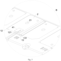
Fig. 1 is a schematic structural diagram in a perspective view of the signal collecting component provided in an embodiment of the present disclosure; -
Fig. 2 is a schematic diagram in a partially enlarged view of the structure inFig. 1 at A; -
Fig. 3 is a schematic diagram in a partially enlarged view of the structure inFig. 1 at B; and -
Fig. 4 is a schematic diagram in a partially enlarged view of the structure inFig. 1 at C. - 1 plastic support; 11 extension bracket; 12 limit groove; 121 accommodating groove; 13 elastic tab; 131 snap-projection; 14 limit post; 2 busbar; 21 inspection hole; 3 first PCB; 31 first connector; 4 FFC; 41 collecting nickel sheet; 411 nickel extension part; 412 snap-fit sheet; 5 second PCB; 6 protective cover.
- Referring to
Figs. 1-4 , a signal collecting component, applied to a battery module, includes aplastic support 1, abusbar 2, a firstprinted circuit board 3, PCB, and a flexibleflat cable 4, FFC. Thebusbar 2 is configured on a side of theplastic support 1 facing away from cells. Thefirst PCB 3 is configured on the plastic support, and an active front end, AFE, is integrated on the first PCB. The FFC is provided with an input port and an output port, in which the input port is connected to each busbar, and the output port is electrically connected to the AFE. - In some implementations, the input port of the
FFC 4 is configured with a collectingnickel sheet 41, and the input port of theFFC 4 is connected to thebusbars 2 through a collectingnickel sheet 41 for collecting voltage data of the cells. Thefirst PCB 3 is integrally provided with the AFE, and a connection between theFFC 4 and AFE is achieved through thefirst PCB 3. In such an arrangement, compared to the traditional long-distance and multi-line connection betweenFFC 4 and BMS (not shown in figures), it may effectively shorten the connection distance between the signal collecting component and AFE, thereby effectively reducing the interference in the process of transmitting signals from theFFC 4 to the AFE, and guaranteeing the accuracy of signal transmission. Also, the AFE converts the analog signals collected through theFFC 4 into digital signals at the signal collecting component, therefore only two intermediate cables are necessary to transfer the signals to the BMS, resulting in a small number of intermediate cables, low cost, and two cables that are easy to comb, which greatly reduces the failure rate at this position. - Specifically, in some implementations, the first PCB 3 is integrally configured with a
first connector 31, theconnector 31 is configured to be connected to a battery management system, BMS, and thefirst connector 31 is electrically connected to the AFE. When in use, the BMS is configured with a second connector adapted to thefirst connector 31, and thefirst connector 31 and the second connector are in inserted connection to achieve the connection between the signal collecting component and the BMS. Optionally, thefirst connector 31 and the second connector are two-core connectors. - As shown in
Fig. 2 , theplastic support 1 is configured with anextension bracket 11, the output port of the FFC 4 is extended to theextension bracket 11, and the first PCB 3 is provided on theextension bracket 11. In some implementations, theextension bracket 11 and theplastic support 1 are integrally injection molded. By setting thefirst PCB 3 on theextension bracket 11, it may be avoided that thefirst PCB 3 affects a layout and arrangement of thebusbars 2 and theFFC 4 on theplastic support 1, which is conducive to keeping the neatness of the signal collecting component. - In some implementations, the
extension bracket 11 is configured with alimit post 14, thelimit post 14 penetrates thefirst PCB 3, and thelimit post 14 is configured to restrict a position of thefirst PCB 3. In some implementations, thelimit post 14 may be a hot-riveting post. In some other implementations, thelimit post 14 may be cooperated with a nut (not shown in figures), so that the nut and thelimit post 14 are in a threaded connection to fixedly abut the first PCB to theextension bracket 11. - The
plastic support 1 is rectangular plate in shape, and theextension bracket 11 is positioned on an end of a length direction of theplastic support 1. In some implementations, thebusbar 2 is arranged along a length direction of theplastic support 1, and the FFC 4 extends along the length direction of theplastic support 1. - As shown in
Fig. 3 , theplastic support 1 is configured with a limit structure, and the limit structure is configured to restrict positions of thebusbars 2. The limit structure herein is configured to fixedly restrict thebusbars 2 on theplastic support 1, so as to achieve an integration of the signal collecting component. - Specifically, the limit structure includes an
elastic tab 13 configured on theplastic support 1, eachelastic tab 13 is configured with a snap-projection 131, and eachbusbar 2 is positioned between the corresponding snap-projection 131 and theplastic support 1 when eachbusbar 2 is assembled to theplastic support 1. Theelastic tab 13 herein is integrally molded with theplastic holder 1 and has elastic deformability. When in use, when thebusbar 2 is assembled to theplastic support 1 and abutted against the snap-projection 131, theelastic tab 13 is elastically deformed by a force to enable thebusbar 2 to move toward theplastic support 1 until thebusbar 2 is positioned between theplastic support 1 and the snap-projection 131, at which time theelastic tab 13 is reset, and the snap-projection 131 cooperates with theplastic support 1 in limiting thebusbar 2. In some implementations, there may be a limit structure, which are only necessary arranged at positions for mounting the busbars. - In some implementations, the
plastic support 1 is provided with alimit groove 12 adapted to each of thebusbars 2, and each of thebusbars 2 is embedded into thecorresponding limit groove 12. Thelimit grooves 12 herein are configured to embed thebusbars 2, which is able to lead to a reduction of an overall thickness of the signal collecting component, and also facilitate the positioning assembly between thebusbars 2 and theplastic support 1. - In some implementations, at least a part of an inner wall of the
limit groove 12 is abutted against thecorresponding busbar 2. That is, the inner wall of thelimit groove 12 is able to restrict a position of thebusbar 2 when thebusbar 2 is assembled into thelimit groove 12, serving as a function of the aforementioned limit structure. In such an arrangement, theelastic tab 13 mentioned above may be omitted. - For facilitate description, in below implementations, a scenario in which the
limit groove 12 is employed with anelastic tab 13 is taken as an example for illustration. - Specifically, as shown in
Fig. 3 , the inner wall of thelimit groove 12 is provided with anaccommodating groove 121, anelastic tab 13 is configured in theaccommodating groove 121, theelastic tab 13 is configured with a snap-projection 131, and eachbusbar 2 is positioned between the corresponding snap-projection 131 and a bottom wall of eachlimit groove 12 when eachbusbars 2 is assembled to thelimit groove 12. Theaccommodating groove 121 herein is capable of accommodating theelastic tab 13, thereby facilitating a reduction in a thickness of the signal collecting component. In some implementations, thebusbar 2 and the inner wall of thelimit groove 12 may be a tight fit or a loose fit. - As shown in
Fig. 3 , in some implementations, eachbusbar 2 is provided with an inspection hole 21and theinspection hole 21 penetrates eachbusbar 2. Theinspection holes 21 herein facilitate inspection of the welding between thebusbars 2 and the cells, such as whether there is any deficient welding between thebusbars 2 and the cells. - In some implementations, as shown in
Figs. 1 and4 , the signal collecting component further includes a temperature sensor (not shown in figures) mounted on at least one of thebusbars 2, and the temperature sensor is electrically connected to theFFC 4. The temperature sensor herein is configured to collect a temperature signal of acorresponding busbar 2, i.e., a corresponding cell. - In some implementations, the collecting
nickel sheet 41 for assembling the temperature sensor is configured with a snap-fit structure 7, and the snap-fit structure 7 is configured to be in detachable connection with the temperature sensor. The snap-fit structure 7 herein facilitates the disassembly and assembly of the temperature sensor, and facilitates the maintenance of the temperature sensor in later use. - Specifically, the snap-fit structure 7 includes snap-fit sheets 412, two snap-fit sheets 412 are configured oppositely on the collecting
nickel sheet 41 for assembling the temperature sensor, and a snap groove for being snap-fitted with the temperature sensor is formed between two snap-fit sheets 412. When in use, it is sufficient to insert the temperature sensor into the snap groove. Optionally, in some implementations, the snap-fit sheets 412 have elastic deformability, so that it allows the temperature sensor to be held more securely without compromising its removal efficiency. - More specifically, in some implementations, the signal collecting component further includes a
second PCB 5 mounted on theplastic support 1, the second PCB corresponds to the collectingnickel sheet 41 for assembling the temperature sensor, the collectingnickel sheet 41 for assembling the temperature sensor is configured with anickel extension part 411, the snap-fit sheets 412 are configured on thenickel extension part 411, and the temperature sensor is electrically connected to the input port of theFFC 4 through thesecond PCB 5. Optionally, thesecond PCB 5 may be connected to theplastic support 1 by a snap-fitting connection, or by a screw, or by a hot-riveting post. The assembly of thesecond PCB 5 and theplastic support 1 may facilitate a precise assembly of the temperature sensor and theFFC 4, and the signal transmission line between the temperature sensor and theFFC 4 is secure, which guarantees the reliability of the signal transmission between the temperature sensor and theFFC 4 during use. - As shown in
Fig. 2 , in some implementations, theFFC 4 is provided with a fuse (not shown in figures), and the fuse is provided close to thefirst PCB 3. Thefirst PCB 3 is provided with aprotective cover 6, and the fuse is positioned between theprotective cover 6 and thefirst PCB 3. The fuse herein serves as a safety guard. Specifically, a short-circuit loop is cut off by the fuse when the signal collecting component is short-circuited due to insulation failure. Theprotective cover 6 is configured to protect the fuse from being damaged by external forces. - It should be noted that the
protective cover 6 is made of a transparent material. Optionally, the material of theprotective cover 6 includes, but is not limited to, such as transparent polycarbonate (PC) or transparent polyvinylchloride (PVC). - Provided in the present disclosure is also a battery module, including a plurality of cells and the aforementioned signal collecting component, and the plurality of cells are arranged along a length direction of the
plastic support 1 and are connected in series by means of the busbars. In some implementations, thebusbars 2 pass through theplastic support 1 to be connected to the cells. This battery module facilitates signal collection and is able to accurately transmitting signals to the BMS with high safety.
Claims (20)
- A signal collecting component, applied to a battery module, the battery module comprising cells, the signal collecting component comprising:a plastic support (1);a busbar (2), configured on a side of the plastic support (1) facing away from the cells;a first printed circuit board (3), PCB, configured on the plastic support (1), wherein an active front end, AFE, is integrated on the first PCB (3); anda flexible flat cable (4), FFC, provided with an input port and an output port, wherein the input port is connected to each of the busbars (2), and the output port is electrically connected to the AFE.
- The signal collecting component according to claim 1, wherein the first PCB is integrally configured with a first connector (31), the connector (31) is configured to be connected to a battery management system, BMS, and the first connector (31) is electrically connected to the AFE.
- The signal collecting component according to claim 1, wherein the plastic support (1) is configured with an extension bracket (11), the output port of the FFC (4) is extended to the extension bracket (11), and the first PCB (3) is provided on the extension bracket (11).
- The signal collecting component according to claim 3, wherein the extension bracket (11) is configured with a limit post (14), the limit post (14) penetrates the first PCB (3), and the limit post (14) is configured to restrict a position of the first PCB (3).
- The signal collecting component according to claim 3, wherein the extension bracket (11) and the plastic support (1) are integrally molded.
- The signal collecting component according to claim 1, wherein the plastic support (1) is configured with a limit structure, and the limit structure is configured to restrict positions of the busbars (2).
- The signal collecting component according to claim 6, wherein the limit structure comprises an elastic tab (13) configured on the plastic support (1), each elastic tab (13) is configured with a snap-projection (131), and each of the busbars (2) is positioned between the corresponding snap-projection (131) and the plastic support (1) when each of the busbars (2) is assembled to the plastic support (1).
- The signal collecting component according to claim 1, wherein the plastic support (1) is configured with a limit groove (12) adapted to each of the busbars (2), and each of the busbars (2) is embedded into the corresponding limit groove (12).
- The signal collecting component according to claim 8, wherein at least a part of an inner wall of the limit groove (12) is abutted against the corresponding busbar (2).
- The signal collecting component according to claim 8 or 9, wherein an inner wall of the limit groove (12) is provided with an accommodating groove (121), an elastic tab (13) is configured in the accommodating groove (121), the elastic tab (13) is configured with a snap-projection (131), and each of the busbars (2) is positioned between the corresponding snap-projection (131) and a bottom wall of each of the limit grooves (12) when each of the busbars (2) is assembled to each of the limit grooves (12).
- The signal collecting component according to claim 1, wherein an inspection hole (21) provided penetrating each of the busbars (2).
- The signal collecting component according to claim 1, further comprising a temperature sensor mounted to at least one of the busbars (2), and the temperature sensor is electrically connected to the FFC (4).
- The signal collecting component according to claim 12, wherein the FFC (4) is connected to the busbars (2) through a collecting nickel sheet (41), the collecting nickel sheet (41) for assembling the temperature sensor is configured with a snap-fit structure (7), and the snap-fit structure (7) is configured to be in detachable connection with the temperature sensor.
- The signal collecting component according to claim 13, wherein the snap-fit structure (7) comprises snap-fit sheets (412), two snap-fit sheets (412) are configured oppositely on the collecting nickel sheet (41) for assembling the temperature sensor, a snap groove is formed between two snap-fit sheets (412), and the snap groove is configured to be snap-fitted with the temperature sensor.
- The signal collecting component according to claim 14, further comprising a second PCB (5) mounted on the plastic support (1), the second PCB corresponds to the collecting nickel sheet (41) for assembling the temperature sensor,the collecting nickel sheet (41) for assembling the temperature sensor is configured with a nickel extension part (411), the snap-fit sheets (412) are configured on the nickel extension part (411), andthe temperature sensor is electrically connected to the input port of the FFC (4) through the second PCB (5).
- The signal collecting component according to claim 1, wherein the FFC (4) is configured with a fuse.
- The signal collecting component according to claim 16, wherein the fuse is closed to the first PCB (3),
the first PCB (3) is configured with a protective cover (6), and the fuse is positioned between the protective cover (6) and the first PCB (3). - The signal collecting component according to claim 17, wherein the protective cover (6) is made of a transparent material.
- A battery module, comprising the signal collecting component according to any one of claims 1-18.
- The battery module according to claim 19, wherein the battery module comprises a plurality of cells, the plurality of cells are arranged along a length direction of the plastic support (1),
and the busbars (2) pass through the plastic support (1) to be connected to the plurality of cells, so that the plurality of cells are connected in series.
Applications Claiming Priority (1)
| Application Number | Priority Date | Filing Date | Title |
|---|---|---|---|
| CN202322483738.5U CN220856841U (en) | 2023-09-12 | 2023-09-12 | Signal acquisition components and battery modules |
Publications (1)
| Publication Number | Publication Date |
|---|---|
| EP4525185A1 true EP4525185A1 (en) | 2025-03-19 |
Family
ID=90787274
Family Applications (1)
| Application Number | Title | Priority Date | Filing Date |
|---|---|---|---|
| EP24199801.2A Pending EP4525185A1 (en) | 2023-09-12 | 2024-09-11 | Signal collecting component and battery module |
Country Status (5)
| Country | Link |
|---|---|
| US (1) | US20250087765A1 (en) |
| EP (1) | EP4525185A1 (en) |
| JP (1) | JP2025040968A (en) |
| CN (1) | CN220856841U (en) |
| WO (1) | WO2025055188A1 (en) |
Citations (3)
| Publication number | Priority date | Publication date | Assignee | Title |
|---|---|---|---|---|
| DE102020101609A1 (en) * | 2019-02-26 | 2020-08-27 | GM Global Technology Operations LLC | BATTERY MODULE WITH INTERCONNECTED BOARD MOUNTING WITH INTEGRATED CELL SENSOR PCB-FLEX CIRCUIT HARDWARE |
| DE102019208769A1 (en) * | 2019-06-17 | 2020-12-17 | Mahle International Gmbh | accumulator |
| EP4089788A1 (en) * | 2021-05-10 | 2022-11-16 | Yazaki Corporation | Busbar module |
Family Cites Families (6)
| Publication number | Priority date | Publication date | Assignee | Title |
|---|---|---|---|---|
| JP5800671B2 (en) * | 2011-08-01 | 2015-10-28 | 矢崎総業株式会社 | Connection control body for battery pack |
| KR102851974B1 (en) * | 2019-10-10 | 2025-08-27 | 주식회사 엘지에너지솔루션 | Battery Pack with improved series connection and voltage sensing scheme |
| CN217334309U (en) * | 2022-05-17 | 2022-08-30 | 芜湖天弋能源科技有限公司 | Integrated CCS module |
| CN218939948U (en) * | 2022-12-26 | 2023-04-28 | 合肥国轩高科动力能源有限公司 | Integrated converging module |
| CN116169530A (en) * | 2022-12-29 | 2023-05-26 | 湖北亿纬动力有限公司 | Signal transfer module and battery pack |
| CN116632465B (en) * | 2023-07-19 | 2023-10-27 | 中国第一汽车股份有限公司 | Direct-connection battery module, design method thereof, battery pack and vehicle |
-
2023
- 2023-09-12 CN CN202322483738.5U patent/CN220856841U/en active Active
- 2023-12-19 WO PCT/CN2023/139704 patent/WO2025055188A1/en active Pending
-
2024
- 2024-09-11 JP JP2024157252A patent/JP2025040968A/en active Pending
- 2024-09-11 US US18/830,611 patent/US20250087765A1/en active Pending
- 2024-09-11 EP EP24199801.2A patent/EP4525185A1/en active Pending
Patent Citations (3)
| Publication number | Priority date | Publication date | Assignee | Title |
|---|---|---|---|---|
| DE102020101609A1 (en) * | 2019-02-26 | 2020-08-27 | GM Global Technology Operations LLC | BATTERY MODULE WITH INTERCONNECTED BOARD MOUNTING WITH INTEGRATED CELL SENSOR PCB-FLEX CIRCUIT HARDWARE |
| DE102019208769A1 (en) * | 2019-06-17 | 2020-12-17 | Mahle International Gmbh | accumulator |
| EP4089788A1 (en) * | 2021-05-10 | 2022-11-16 | Yazaki Corporation | Busbar module |
Also Published As
| Publication number | Publication date |
|---|---|
| WO2025055188A1 (en) | 2025-03-20 |
| JP2025040968A (en) | 2025-03-25 |
| US20250087765A1 (en) | 2025-03-13 |
| CN220856841U (en) | 2024-04-26 |
Similar Documents
| Publication | Publication Date | Title |
|---|---|---|
| US20200350636A1 (en) | Battery module and battery pack | |
| EP3699979B1 (en) | Battery module | |
| US9991645B2 (en) | Cell contact-making system for an electrochemical device | |
| US9301025B2 (en) | Removable sensor modules | |
| US10741817B2 (en) | Battery connection module | |
| CN115411468A (en) | Busbar assembly and battery assembly | |
| CN209947993U (en) | Battery cell information acquisition structure of battery pack | |
| CN216488226U (en) | Battery module integrated acquisition assembly and battery module | |
| EP3715171B1 (en) | Flexprint for energy storage module | |
| WO2024245452A1 (en) | Ccs protective cap, ccs assembly and battery pack | |
| US20150024239A1 (en) | Cover for Batteries | |
| US20250087765A1 (en) | Signal collecting component and battery module | |
| EP4099490B1 (en) | Battery module and battery pack including the same | |
| US20250316852A1 (en) | Integrated busbar, bracket thereof, and battery module thereof | |
| CN112564592A (en) | Point-supported photovoltaic module | |
| WO2024113949A1 (en) | Signal acquisition assembly and battery module | |
| CN212876189U (en) | Module flexible circuit board sampling connection structure | |
| EP4485617A1 (en) | Cells contact system, battery, and electric vehicle | |
| CN117060016A (en) | Battery cell | |
| CN214477796U (en) | Connecting assembly based on end side output | |
| CN221201566U (en) | CCS assembly, battery module and battery pack | |
| DE102017125128A1 (en) | Battery assembly and telematics unit | |
| CN221352879U (en) | Temperature sampling unit and battery pack | |
| CN223285223U (en) | Data acquisition device of battery module | |
| CN223858405U (en) | Acquisition device and battery module |
Legal Events
| Date | Code | Title | Description |
|---|---|---|---|
| PUAI | Public reference made under article 153(3) epc to a published international application that has entered the european phase |
Free format text: ORIGINAL CODE: 0009012 |
|
| STAA | Information on the status of an ep patent application or granted ep patent |
Free format text: STATUS: REQUEST FOR EXAMINATION WAS MADE |
|
| 17P | Request for examination filed |
Effective date: 20240911 |
|
| AK | Designated contracting states |
Kind code of ref document: A1 Designated state(s): AL AT BE BG CH CY CZ DE DK EE ES FI FR GB GR HR HU IE IS IT LI LT LU LV MC ME MK MT NL NO PL PT RO RS SE SI SK SM TR |
|
| STAA | Information on the status of an ep patent application or granted ep patent |
Free format text: STATUS: EXAMINATION IS IN PROGRESS |